EP3130595A1 - Organometallische verbindung, organische lichtemittierende vorrichtung mit der organometallischen verbindung und diagnosezusammensetzung mit der organometallischen verbindung - Google Patents
Organometallische verbindung, organische lichtemittierende vorrichtung mit der organometallischen verbindung und diagnosezusammensetzung mit der organometallischen verbindung Download PDFInfo
- Publication number
- EP3130595A1 EP3130595A1 EP16183831.3A EP16183831A EP3130595A1 EP 3130595 A1 EP3130595 A1 EP 3130595A1 EP 16183831 A EP16183831 A EP 16183831A EP 3130595 A1 EP3130595 A1 EP 3130595A1
- Authority
- EP
- European Patent Office
- Prior art keywords
- group
- ring
- substituted
- sec
- tert
- Prior art date
- Legal status (The legal status is an assumption and is not a legal conclusion. Google has not performed a legal analysis and makes no representation as to the accuracy of the status listed.)
- Granted
Links
- 0 CC1*=CC=CCC=C(C)*1N Chemical compound CC1*=CC=CCC=C(C)*1N 0.000 description 59
- SFJCUTLENXGJOA-UHFFFAOYSA-N OC(CC(C(C1(O)O)(O)O)(O)O)(C1(O)O)O Chemical compound OC(CC(C(C1(O)O)(O)O)(O)O)(C1(O)O)O SFJCUTLENXGJOA-UHFFFAOYSA-N 0.000 description 2
- WJQXQBBYKGOORN-UHFFFAOYSA-N CC(C)(C)c1n[nH]c(-c2nc(-c3cc(C(C)(C)C)n[nH]3)cc(-c3cc(C(C)(C)C)cc(C(C)(C)C)c3)c2)c1 Chemical compound CC(C)(C)c1n[nH]c(-c2nc(-c3cc(C(C)(C)C)n[nH]3)cc(-c3cc(C(C)(C)C)cc(C(C)(C)C)c3)c2)c1 WJQXQBBYKGOORN-UHFFFAOYSA-N 0.000 description 1
- KJKBDDLDXPLFAM-UHFFFAOYSA-N CC1(C)c2n[nH]c(-c3nc(-c4c(CCCC5(C)C)c5n[nH]4)c(cccc4)c4c3)c2CCC1 Chemical compound CC1(C)c2n[nH]c(-c3nc(-c4c(CCCC5(C)C)c5n[nH]4)c(cccc4)c4c3)c2CCC1 KJKBDDLDXPLFAM-UHFFFAOYSA-N 0.000 description 1
- RISZXXLFIBVQDC-UHFFFAOYSA-N CC1C(CN)C(CCC2)CC2C1 Chemical compound CC1C(CN)C(CCC2)CC2C1 RISZXXLFIBVQDC-UHFFFAOYSA-N 0.000 description 1
- CLTHBVPJKLDVAS-UHFFFAOYSA-N CCc1cc(C(C)(C)C)cc(C(C)(C)C)c1 Chemical compound CCc1cc(C(C)(C)C)cc(C(C)(C)C)c1 CLTHBVPJKLDVAS-UHFFFAOYSA-N 0.000 description 1
- ZLZOXDZYAUEZID-UHFFFAOYSA-N N[O](CC1)c2c1cccc2 Chemical compound N[O](CC1)c2c1cccc2 ZLZOXDZYAUEZID-UHFFFAOYSA-N 0.000 description 1
- FFYZMBQLAYDJIG-UHFFFAOYSA-N Nc1ccc2[o]c(cccc3)c3c2c1 Chemical compound Nc1ccc2[o]c(cccc3)c3c2c1 FFYZMBQLAYDJIG-UHFFFAOYSA-N 0.000 description 1
- ICMMJWDNKMITSS-UHFFFAOYSA-N Nc1ccc2[s]c(cccc3)c3c2c1 Chemical compound Nc1ccc2[s]c(cccc3)c3c2c1 ICMMJWDNKMITSS-UHFFFAOYSA-N 0.000 description 1
- RCDMUNHSQCVVBJ-UHFFFAOYSA-N Nc1cccc2c1c1ccccc1[o]2 Chemical compound Nc1cccc2c1c1ccccc1[o]2 RCDMUNHSQCVVBJ-UHFFFAOYSA-N 0.000 description 1
Images
Classifications
-
- C—CHEMISTRY; METALLURGY
- C07—ORGANIC CHEMISTRY
- C07F—ACYCLIC, CARBOCYCLIC OR HETEROCYCLIC COMPOUNDS CONTAINING ELEMENTS OTHER THAN CARBON, HYDROGEN, HALOGEN, OXYGEN, NITROGEN, SULFUR, SELENIUM OR TELLURIUM
- C07F15/00—Compounds containing elements of Groups 8, 9, 10 or 18 of the Periodic Table
- C07F15/0006—Compounds containing elements of Groups 8, 9, 10 or 18 of the Periodic Table compounds of the platinum group
-
- C—CHEMISTRY; METALLURGY
- C07—ORGANIC CHEMISTRY
- C07F—ACYCLIC, CARBOCYCLIC OR HETEROCYCLIC COMPOUNDS CONTAINING ELEMENTS OTHER THAN CARBON, HYDROGEN, HALOGEN, OXYGEN, NITROGEN, SULFUR, SELENIUM OR TELLURIUM
- C07F15/00—Compounds containing elements of Groups 8, 9, 10 or 18 of the Periodic Table
- C07F15/0006—Compounds containing elements of Groups 8, 9, 10 or 18 of the Periodic Table compounds of the platinum group
- C07F15/0086—Platinum compounds
- C07F15/0093—Platinum compounds without a metal-carbon linkage
-
- C—CHEMISTRY; METALLURGY
- C07—ORGANIC CHEMISTRY
- C07D—HETEROCYCLIC COMPOUNDS
- C07D401/00—Heterocyclic compounds containing two or more hetero rings, having nitrogen atoms as the only ring hetero atoms, at least one ring being a six-membered ring with only one nitrogen atom
- C07D401/14—Heterocyclic compounds containing two or more hetero rings, having nitrogen atoms as the only ring hetero atoms, at least one ring being a six-membered ring with only one nitrogen atom containing three or more hetero rings
-
- C—CHEMISTRY; METALLURGY
- C09—DYES; PAINTS; POLISHES; NATURAL RESINS; ADHESIVES; COMPOSITIONS NOT OTHERWISE PROVIDED FOR; APPLICATIONS OF MATERIALS NOT OTHERWISE PROVIDED FOR
- C09K—MATERIALS FOR MISCELLANEOUS APPLICATIONS, NOT PROVIDED FOR ELSEWHERE
- C09K11/00—Luminescent materials, e.g. electroluminescent or chemiluminescent
- C09K11/06—Luminescent materials, e.g. electroluminescent or chemiluminescent containing organic luminescent materials
-
- G—PHYSICS
- G01—MEASURING; TESTING
- G01N—INVESTIGATING OR ANALYSING MATERIALS BY DETERMINING THEIR CHEMICAL OR PHYSICAL PROPERTIES
- G01N33/00—Investigating or analysing materials by specific methods not covered by groups G01N1/00 - G01N31/00
- G01N33/48—Biological material, e.g. blood, urine; Haemocytometers
- G01N33/50—Chemical analysis of biological material, e.g. blood, urine; Testing involving biospecific ligand binding methods; Immunological testing
- G01N33/58—Chemical analysis of biological material, e.g. blood, urine; Testing involving biospecific ligand binding methods; Immunological testing involving labelled substances
-
- H—ELECTRICITY
- H05—ELECTRIC TECHNIQUES NOT OTHERWISE PROVIDED FOR
- H05B—ELECTRIC HEATING; ELECTRIC LIGHT SOURCES NOT OTHERWISE PROVIDED FOR; CIRCUIT ARRANGEMENTS FOR ELECTRIC LIGHT SOURCES, IN GENERAL
- H05B33/00—Electroluminescent light sources
- H05B33/12—Light sources with substantially two-dimensional [2D] radiating surfaces
- H05B33/14—Light sources with substantially two-dimensional [2D] radiating surfaces characterised by the chemical or physical composition or the arrangement of the electroluminescent material, or by the simultaneous addition of the electroluminescent material in or onto the light source
-
- H—ELECTRICITY
- H10—SEMICONDUCTOR DEVICES; ELECTRIC SOLID-STATE DEVICES NOT OTHERWISE PROVIDED FOR
- H10K—ORGANIC ELECTRIC SOLID-STATE DEVICES
- H10K50/00—Organic light-emitting devices
-
- H—ELECTRICITY
- H10—SEMICONDUCTOR DEVICES; ELECTRIC SOLID-STATE DEVICES NOT OTHERWISE PROVIDED FOR
- H10K—ORGANIC ELECTRIC SOLID-STATE DEVICES
- H10K85/00—Organic materials used in the body or electrodes of devices covered by this subclass
- H10K85/30—Coordination compounds
- H10K85/341—Transition metal complexes, e.g. Ru(II)polypyridine complexes
- H10K85/346—Transition metal complexes, e.g. Ru(II)polypyridine complexes comprising platinum
-
- C—CHEMISTRY; METALLURGY
- C09—DYES; PAINTS; POLISHES; NATURAL RESINS; ADHESIVES; COMPOSITIONS NOT OTHERWISE PROVIDED FOR; APPLICATIONS OF MATERIALS NOT OTHERWISE PROVIDED FOR
- C09K—MATERIALS FOR MISCELLANEOUS APPLICATIONS, NOT PROVIDED FOR ELSEWHERE
- C09K2211/00—Chemical nature of organic luminescent or tenebrescent compounds
- C09K2211/10—Non-macromolecular compounds
- C09K2211/1018—Heterocyclic compounds
- C09K2211/1025—Heterocyclic compounds characterised by ligands
- C09K2211/1029—Heterocyclic compounds characterised by ligands containing one nitrogen atom as the heteroatom
-
- C—CHEMISTRY; METALLURGY
- C09—DYES; PAINTS; POLISHES; NATURAL RESINS; ADHESIVES; COMPOSITIONS NOT OTHERWISE PROVIDED FOR; APPLICATIONS OF MATERIALS NOT OTHERWISE PROVIDED FOR
- C09K—MATERIALS FOR MISCELLANEOUS APPLICATIONS, NOT PROVIDED FOR ELSEWHERE
- C09K2211/00—Chemical nature of organic luminescent or tenebrescent compounds
- C09K2211/10—Non-macromolecular compounds
- C09K2211/1018—Heterocyclic compounds
- C09K2211/1025—Heterocyclic compounds characterised by ligands
- C09K2211/1044—Heterocyclic compounds characterised by ligands containing two nitrogen atoms as heteroatoms
-
- C—CHEMISTRY; METALLURGY
- C09—DYES; PAINTS; POLISHES; NATURAL RESINS; ADHESIVES; COMPOSITIONS NOT OTHERWISE PROVIDED FOR; APPLICATIONS OF MATERIALS NOT OTHERWISE PROVIDED FOR
- C09K—MATERIALS FOR MISCELLANEOUS APPLICATIONS, NOT PROVIDED FOR ELSEWHERE
- C09K2211/00—Chemical nature of organic luminescent or tenebrescent compounds
- C09K2211/10—Non-macromolecular compounds
- C09K2211/1018—Heterocyclic compounds
- C09K2211/1025—Heterocyclic compounds characterised by ligands
- C09K2211/1059—Heterocyclic compounds characterised by ligands containing three nitrogen atoms as heteroatoms
-
- C—CHEMISTRY; METALLURGY
- C09—DYES; PAINTS; POLISHES; NATURAL RESINS; ADHESIVES; COMPOSITIONS NOT OTHERWISE PROVIDED FOR; APPLICATIONS OF MATERIALS NOT OTHERWISE PROVIDED FOR
- C09K—MATERIALS FOR MISCELLANEOUS APPLICATIONS, NOT PROVIDED FOR ELSEWHERE
- C09K2211/00—Chemical nature of organic luminescent or tenebrescent compounds
- C09K2211/18—Metal complexes
-
- C—CHEMISTRY; METALLURGY
- C09—DYES; PAINTS; POLISHES; NATURAL RESINS; ADHESIVES; COMPOSITIONS NOT OTHERWISE PROVIDED FOR; APPLICATIONS OF MATERIALS NOT OTHERWISE PROVIDED FOR
- C09K—MATERIALS FOR MISCELLANEOUS APPLICATIONS, NOT PROVIDED FOR ELSEWHERE
- C09K2211/00—Chemical nature of organic luminescent or tenebrescent compounds
- C09K2211/18—Metal complexes
- C09K2211/185—Metal complexes of the platinum group, i.e. Os, Ir, Pt, Ru, Rh or Pd
-
- H—ELECTRICITY
- H10—SEMICONDUCTOR DEVICES; ELECTRIC SOLID-STATE DEVICES NOT OTHERWISE PROVIDED FOR
- H10K—ORGANIC ELECTRIC SOLID-STATE DEVICES
- H10K2101/00—Properties of the organic materials covered by group H10K85/00
- H10K2101/10—Triplet emission
-
- H—ELECTRICITY
- H10—SEMICONDUCTOR DEVICES; ELECTRIC SOLID-STATE DEVICES NOT OTHERWISE PROVIDED FOR
- H10K—ORGANIC ELECTRIC SOLID-STATE DEVICES
- H10K50/00—Organic light-emitting devices
- H10K50/10—OLEDs or polymer light-emitting diodes [PLED]
- H10K50/11—OLEDs or polymer light-emitting diodes [PLED] characterised by the electroluminescent [EL] layers
-
- H—ELECTRICITY
- H10—SEMICONDUCTOR DEVICES; ELECTRIC SOLID-STATE DEVICES NOT OTHERWISE PROVIDED FOR
- H10K—ORGANIC ELECTRIC SOLID-STATE DEVICES
- H10K85/00—Organic materials used in the body or electrodes of devices covered by this subclass
- H10K85/30—Coordination compounds
- H10K85/321—Metal complexes comprising a group IIIA element, e.g. Tris (8-hydroxyquinoline) gallium [Gaq3]
- H10K85/324—Metal complexes comprising a group IIIA element, e.g. Tris (8-hydroxyquinoline) gallium [Gaq3] comprising aluminium, e.g. Alq3
Definitions
- One or more aspects of example embodiments of the present disclosure are related to an organometallic compound, an organic light-emitting device including the organometallic compound, and composition for use in diagnosis including the organometallic compound.
- Organic light-emitting devices are self-emission devices, have better characteristics than conventional devices in terms of a viewing angle, a response time, and brightness, a driving voltage, and a response speed, and produce full-color images.
- an organic light-emitting device includes an anode, a cathode, and an organic layer between the anode and the cathode, wherein the organic layer includes an emission layer.
- a hole transport region may be between the anode and the emission layer, and an electron transport region may be between the emission layer and the cathode.
- Holes provided from the anode may move toward the emission layer through the hole transport region, and electrons provided from the cathode may move toward the emission layer through the electron transport region.
- the holes and the electrons recombine in the emission layer to produce excitons. These excitons transition from an excited state to a ground state, thereby generating light.
- luminescent compounds may be used to monitor, sense, or detect a biological material, such as a cell protein.
- a biological material such as a cell protein.
- luminescent compounds include a phosphorescent luminescent compound.
- One or more embodiments include an organometallic compound, an organic light-emitting device including the organometallic compound, and a for use in diagnosis including the organometallic compound.
- an organometallic compound is represented by Formula 1 below: ⁇ Formula 1> M(L 1 )(L 2 )
- M may be beryllium (Be), magnesium (Mg), aluminium (Al), calcium (Ca), titanium (Ti), manganese (Mn), cobalt (Co), copper (Cu), zinc (Zn), gallium (Ga), germanium (Ge), zirconium (Zr), rutheium (Ru), rhodium (Rh), palladium (Pd), silver (Ag), rhenium (Re), platinum (Pt) or gold (Au),
- L 1 may be selected from tridentate ligands represented by Formula 2
- L 2 may be selected from monodentate organic ligands, *, *', and *" in Formula 2 each indicate a binding site to M in Formula 1
- Y 1 to Y 3 may each be nitrogen (N)
- Y 4 and Y 5 may each be carbon (C)
- a bond between Y 1 and Y 4 may be a single bond or a double bond
- a bond between Y 2 and Y 5 may be a single bond or a
- an organic light-emitting device includes: a first electrode; a second electrode; and an organic layer between the first electrode and the second electrode, the organic layer including an emission layer, wherein the organic layer includes one or more selected from the organometallic compounds.
- the organometallic compounds may act as a dopant in the emission layer.
- a composition for use in diagnosis includes one or more selected from the organometallic compounds represented by Formula 1.
- Diagnosis in the sense of the invention refers to both in vivo and in vitro diagnosis.
- M in Formula 1 may be beryllium (Be), magnesium (Mg), aluminium (Al), calcium (Ca), titanium (Ti), manganese (Mn), cobalt (Co), copper (Cu), zinc (Zn), gallium (Ga), germanium (Ge), zirconium (Zr), rutheium (Ru), rhodium (Rh), palladium (Pd), silver (Ag), rhenium (Re), platinum (Pt) or gold (Au).
- M in Formula 1 may be platinum (Pt).
- L 1 in Formula 1 may be selected from tridentate ligands represented by Formula 2, L 2 may be selected from monodentate organic ligands, and *, *', and *" in Formula 2 each indicate a binding site to M in Formula 1.
- Y 1 to Y 3 may be nitrogen (N)
- Y 4 and Y 5 may be carbon (C)
- a bond between Y 1 and Y 4 may be a single bond or a double bond
- a bond between Y 2 and Y 5 may be a single bond or a double bond.
- one selected from a bond between Y 1 and M, a bond between Y 2 and M, and a bond between ligand L 2 and M may be a coordinate bond, and the other two may be a covalent bond. Also, a bond between Y 3 and M may be a coordinate bond. Therefore, the organometallic compound represented by Formula 1 is in a neutral state having no electric charge.
- a bond between Y 1 and M and a bond between Y 2 and M may be a covalent bond
- a bond between Y 3 and M and a bond between ligand L 2 and M may be a coordinate bond
- a bond between Y 1 and M and a bond between ligand L 2 and M may be a covalent bond
- a bond between Y 3 and M and a bond between Y 2 and M may be a coordinate bond
- Rings A 1 and A 2 in Formula 2 may each independently be selected from a pyrrole ring, a pyrazole ring, an imidazole ring, an oxazole ring, an iso-oxazole ring, an oxadiazole ring, a thiazole ring, an isothiazole ring, and a thiadiazol ring. Accordingly, rings A 1 and A 2 may include one or two nitrogen atoms as a ring-forming atom.
- X 1 may be N or C(R 3 ), X 2 may be N or C(R 4 ), and X 3 may be N or C(R 5 ).
- Two or more selected from R 3 to R 5 may be optionally connected to each other to form a substituted or unsubstituted C 5 -C 30 carbocyclic group or a substituted or unsubstituted C 2 -C 30 heterocyclic group (for example, a substituted or unsubstituted cyclopentadiene group, a substituted or unsubstituted cyclopentane group, a substituted or unsubstituted cyclohexane group, a substituted or unsubstituted adamantane group, a substituted or unsubstituted bicyclo[2.2.1]heptane group, a substituted or unsubstituted benzene group, a substituted or unsubstituted pyridine group, a substituted or unsubstit
- Ring A 3 in Formula 2 may have one or two nitrogen atoms as a ring-forming atom.
- a moiety represented by in Formula 2 and a moiety represented by in Formula 2 may be identical to each other.
- a moiety represented by in Formula 2 and a moiety represented by in Formula 2 may be different from each other.
- At least one selected from rings A 1 and A 2 in Formula 2 may be pyrazol ring.
- both rings A 1 and A 2 in Formula 2 may be a pyrazol ring, but embodiments of the present disclosure are not limited thereto.
- R 6 and R 7 may be optionally connected to each other to form a substituted or unsubstituted C 5 -C 30 carbocyclic group or a substituted or unsubstituted C 2 -C 30 heterocyclic group (for example, a substituted or unsubstituted cyclopentane group, a substituted or unsubstituted cyclohexane group, a substituted or unsubstituted benzene group, a substituted or unsubstituted naphthalene group, and the like).
- R 6 and R 7 are the same as described below.
- a1 and a2 in Formula 1 may each independently be an integer selected from 1 to 3.
- a1 indicates the number of T 1 (s), wherein, when a1 is two or more, two or more T 1 (s) may be identical to or different from each other.
- a2 indicates the number of T 2 (s), wherein, when a2 is two or more, two or more T 2 (s) may be identical to or different from each other.
- a1 and a2 may each independently be 1 or 2.
- T 1 and T 2 in Formula 1 may be a single bond, but embodiments of the present disclosure are not limited thereto.
- a moiety represented by in Formula 2 may not be and a moiety represented by in Formula 2 may not be
- a moiety represented by in Formula 2 may be represented by one selected from Formulae 3-1 to 3-25 and 3-31 to 3-74, a moiety represented by in Formula 2 may be represented by one selected from Formulae 4-1 to 4-25 and 4-31 to 4-74, and a moiety represented by in Formula 2 may be represented by Formulae 5-1 to 5-47:
- Y 7 and Y 8 may each independently be O or S
- Y 9 may be O, S or N(R 39 )
- R 3 to R 5 are the same as described above
- R 11 to R 20 are each independently the same as described above in connection with R 1
- R 21 to R 30 are each independently the same as described above in connection with R 2
- R 31 to R 39 are each independently the same as described above in connection with R 3
- c3 may be an integer selected from 0 to 3
- c4 may be an integer selected from 0 to 4
- c6 may be an integer selected from 0 to 6
- c8 may be an integer selected from 0 to 8
- c10 may be an integer selected from 0 to 10
- *, *', and *" each indicate a binding site to M in Formula 1.
- R 3 to R 5 and R 11 to R 39 in Formulae 3-1 to 3-25, 3-31 to 3-74, 4-1 to 4-25, 4-31 to 4-74, and 5-1 to 5-47 are the same as described below.
- R 1 to R 7 and R 11 to R 39 may each independently be selected from hydrogen, deuterium, -F, -Cl, -Br, -I, -SF 5 , a hydroxyl group, a cyano group, a nitro group, an amino group, an amidino group, a hydrazine group, a hydrazone group, a carboxylic acid group or a salt thereof, a sulfonic acid group or a salt thereof, a phosphoric acid group or a salt thereof, a substituted or unsubstituted C 1 -C 60 alkyl group, a substituted or unsubstituted C 2 -C 60 alkenyl group, a substituted or unsubstituted C 2 -C 60 alkyny
- R 1 to R 7 and R 11 to R 39 may each independently be selected from:
- R 1 to R 7 and R 11 to R 39 may each independently be selected from:
- R 1 to R 7 and R 11 to R 39 may each independently be selected from hydrogen, deuterium, -F, a cyano group, a nitro group, -SF 5 , -CH 3 , -CD 3 , -CD 2 H, -CDH 2 , -CF 3 , -CF 2 H, -CFH 2 , a group represented by any of Formulae 9-1 to 9-19, a group represented by any of Formulae 10-1 to 10-38, and -Si(Q 3 )(Q 4 )(Q 5 ) (descriptions for Q 3 to Q 5 are the same as described in this disclosure), but embodiments of the present disclosure are not limited thereto: * in Formulae 9-1 to 9-19 and 10-1 to 10-38 indicates a binding site to a neighboring atom.
- b1 and b2 in Formula 2 may each independently be an integer selected from 0 to 3, wherein, when b1 is two or more, two or more R 1 (s) may be identical to or different from each other, and when b2 is two or more, two or more R 2 (s) may be identical to or different from each other.
- Two selected from R 1 (s) in the number of b1 in Formula 2 may be optionally connected to each other to form a substituted or unsubstituted C 5 -C 30 carbocyclic group or a substituted or unsubstituted C 2 -C 30 heterocyclic group (for example, a substituted or unsubstituted cyclopentane group, a substituted or unsubstituted cyclohexane group, a substituted or unsubstituted adamantane group, a substituted or unsubstituted bicyclo[2.2.1]heptane group, a substituted or unsubstituted benzene group, a substituted or unsubstituted pyridine group, a substituted or unsubstituted pyrimidine group, a substituted or unsubstituted pyrazine group, a substituted or unsubstituted pyridazine group, a substituted or unsubsti
- Two selected from R 2 (s) in the number of b2 in Formula 2 may be optionally connected to each other to form a substituted or unsubstituted C 5 -C 30 carbocyclic group or a substituted or unsubstituted C 2 -C 30 heterocyclic group (for example, a substituted or unsubstituted cyclopentane group, a substituted or unsubstituted cyclohexane group, a substituted or unsubstituted adamantane group, a substituted or unsubstituted bicyclo[2.2.1]heptane group, a substituted or unsubstituted benzene group, a substituted or unsubstituted pyridine group, a substituted or unsubstituted pyrimidine group, a substituted or unsubstituted pyrazine group, a substituted or unsubstituted pyridazine group, a substituted or unsubsti
- a moiety represented by in Formula 2 may be represented by one selected from Formulae 3-5 to 3-8, 3-23, 3-25, and 3-47 to 3-62, and a moiety represented by in Formula 2 may be represented by one selected from Formulae 4-5 to 4-8, 4-23, 4-25, and 4-47 to 4-62.
- a moiety represented by in Formula 2 may be represented by one selected from Formulae 3-1, 3-5, 3-9, 3-13, 3-31 to 3-34, and 3-47 to 3-50, and a moiety represented by in Formula 2 may be represented by one selected from Formulae 4-1, 4-5, 4-9, 4-13, 4-31 to 4-34, and 4-47 to 4-50.
- a moiety represented by in Formula 2 may be represented by one selected from Formulae 3-1, 3-5, 3-9, 3-13, 3-31 to 3-34, and 3-47 to 3-50, and a moiety represented by in Formula 2 may be represented by one selected from Formulae 4-2 to 4-4, 4-6 to 4-8, 4-10 to 4-12, 4-14 to 4-30, 4-35 to 4-46, and 4-51 to 4-74.
- a moiety represented by in Formula 2 may be represented by one selected from Formulae 5-1 to 5-28, 5-29, and 5-45.
- a moiety represented by in Formula 2 may be represented by one selected from Formulae 3-5 and 3-47 to 3-50, a moiety represented by in Formula 2 may be represented by one selected from Formulae 4-1, 4-5, 4-31 to 4-34, and 4-47 to 4-50, and a moiety represented by in Formula 2 may be represented by one selected from Formulae 5-1, 5-3 to 5-5, 5-7, 5-8, 5-29, and 5-45, but embodiments are not limited thereto.
- L 1 in Formula 1 may be selected from ligands represented by Formulae 2A-1 to 2E-1 and 2A-2 to 2E-2, but embodiments of the present disclosure are not limited thereto:
- R 3 to R 5 , R 11 to R 18 , R 21 to R 28 , and R 31 to R 34 are the same as described above, and *, *', and *" each indicate a binding site to M in Formula 1.
- R 3 to R 5 , R 11 to R 18 , R 21 to R 28 , and R 31 to R 34 in Formulae 2A-1 to 2E-1 and 2A-2 to 2E-2 may each independently be selected from hydrogen, deuterium, -F, a cyano group, a nitro group, -SF 5 , -CH 3 , -CD 3 , -CD 2 H, -CDH 2 , -CF 3 , -CF 2 H, -CFH 2 , a group represented by any of Formulae 9-1 to 9-19, a group represented by any of Formulae 10-1 to 10-38, and -Si(Q 3 )(Q 4 )(Q 5 ) (descriptions for Q 3 to Q 5 are the same as described in this disclosure), but embodiments of the present disclosure are not limited thereto.
- L 2 in Formula 1 may be selected from ligands represented by Formula 6-1: *( ⁇ T 3 ) a3 -R 61 Formula 6-1
- R 61 may each independently be selected from hydrogen, deuterium, -F, -Cl, -Br, -I, -SF 5 , a hydroxyl group, a cyano group, a nitro group, an amino group, an amidino group, a hydrazine group, a hydrazone group, a carboxylic acid group or a salt thereof, a
- R 61 may be selected from:
- L 2 in Formula 1 may be selected from ligands represented by Formulae 12-1 to 12-5, but embodiments of the present disclosure are not limited thereto: wherein, in Formulae 12-1 to 12-5,
- L 2 in Formula 1 may be selected from ligands represented by Formulae 13-1 to 13-47 and 14-1 to 14-28, but embodiments of the present disclosure are not limited thereto:
- R 61 may be selected from:
- the organometallic compound represented by Formula 1 may be one selected from Compounds 1 to 142, but embodiments of the present disclosure are not limited thereto:
- Ligand L 1 in the organometallic compound represented by Formula 1 may be selected from ligands represented by Formula 2, and rings A 1 , A 2 , and A 3 in Formula 2 may have one or two nitrogen atoms as a ring-forming atom.
- the organometallic compound represented by Formula 1 is easy in terms of energy transfer from a host, as compared with a compound (for example, see Compound A) that has the same structure as the organometallic compound represented by Formula 1, provided that rings A 1 , A 2 , and A 3 in Formula 2 have three or more nitrogen atoms. Therefore, an electronic device, for example, an organic light-emitting device, which includes the organometallic compound represented by Formula 1, may have high efficiency.
- Y 3 in Formula 2 may be nitrogen, and a bond between Y 3 in Formula 2 and M in Formula 1 may be a coordinate bond. Therefore, an electronic device, for example, an organic light-emitting device, which includes the organometallic compound represented by Formula 1, may have high luminescent efficiency, high power efficiency, high quantum efficiency, and a long lifespan.
- the highest occupied molecular orbital (HOMO), lowest unoccupied molecular orbital (LUMO), singlet (S 1 ) energy level, and triplet (T 1 ) energy level of Compounds 1, 2, 7, 8, 9, 10, 11, and 12 and Compounds A to C were evaluated by using a density functional theory (DFT) method of a Gaussian program (the structure was optimized at B3LYP, 6-31 G(d,p) level). Results thereof are shown in Table 1. [Table 1] Compound No.
- the organometallic compound represented by Formula 1 has electric characteristics suitable for use in an electronic device, for example, a dopant of an organic light-emitting device.
- an electronic device for example, a dopant of an organic light-emitting device.
- the luminescent efficiency and lifespan of an electronic device for example, an organic light-emitting device, which includes Compound A or B, is poorer than the luminescent efficiency and lifespan of an electronic device, for example, an organic light-emitting device, which includes one selected from Compounds 1, 2, 7, 8, 9, 10, 11, and 12.
- Synthesis methods of the organometallic compound represented by Formula 1 may be recognizable by one of ordinary skill in the art by referring to Synthesis Examples provided below.
- the organometallic compound represented by Formula 1 is suitable for use in an organic layer of an organic light-emitting device, for example, for use as a dopant in an emission layer of the organic layer.
- an organic light-emitting device that includes: a first electrode; a second electrode; and an organic layer between the first electrode and the second electrode and includes an emission layer and at least one of the organometallic compounds represented by Formula 1.
- the organic light-emitting device may have, due to the inclusion of an organic layer including the organometallic compound represented by Formula 1, low driving voltage, high luminescent efficiency, high power efficiency, high quantum efficiency, long lifespan, and excellent color.
- the organometallic compound of Formula 1 may be used between a pair of electrodes of an organic light-emitting device.
- the organometallic compound represented by Formula 1 may be included in the emission layer.
- the organometallic compound may act as a dopant, and the emission layer may further include a host (that is, an amount of the organometallic compound represented by Formula 1 is smaller than an amount of the host).
- organometallic compounds used herein may include a case in which "(an organic layer) includes identical organometallic compounds represented by Formula 1" and a case in which "(an organic layer) includes two or more different organometallic compounds represented by Formula 1".
- the organic layer may include only Compound 1 as the organometallic compound.
- Compound 1 may exist only in the emission layer of the organic light-emitting device.
- the organic layer may include, as the organometallic compound, Compound 1 and Compound 2.
- Compound 1 and Compound 2 may exist in an identical layer (for example, Compound 1 and Compound 2 all may exist in an emission layer).
- the first electrode may be an anode, which is a hole injection electrode, and the second electrode may be a cathode, which is an electron injection electrode; or the first electrode may be a cathode, which is an electron injection electrode, and the second electrode may be an anode, which is a hole injection electrode.
- the first electrode is an anode
- the second electrode is a cathode
- the organic layer includes a hole transport region between the first electrode and the emission layer and an electron transport region between the emission layer and the second electrode
- the hole transport region includes at least one selected from a hole injection layer, a hole transport layer, and an electron blocking layer
- the electron transport region includes at least one selected from a hole blocking layer, an electron transport layer, and an electron injection layer.
- organic layer refers to a single layer and/or a plurality of layers between the first electrode and the second electrode of the organic light-emitting device.
- the “organic layer” may include, in addition to an organic compound, an organometallic complex including metal.
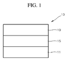
- FIG. 1 is a schematic view of an organic light-emitting device 10 according to an embodiment.
- the organic light-emitting device 10 includes a first electrode 11, an organic layer 15, and a second electrode 19, which are sequentially stacked.
- a substrate may be additionally disposed under the first electrode 11 or above the second electrode 19.
- the substrate any substrate that is used in general organic light-emitting devices may be used, and the substrate may be a glass substrate or a transparent plastic substrate, each having excellent mechanical strength, thermal stability, transparency, surface smoothness, ease of handling, and water-resistance.
- the first electrode 11 may be formed by depositing or sputtering a material for forming the first electrode 11 on the substrate.
- the first electrode 11 may be an anode.
- the material for forming the first electrode 11 may be selected from materials with a high work function to facilitate hole injection.
- the first electrode 11 may be a reflective electrode, a semi-transmissive electrode, or a transmissive electrode.
- the material for forming the first electrode 11 may be, for example, indium tin oxide (ITO), indium zinc oxide (IZO), tin oxide (SnO 2 ), and zinc oxide (ZnO).
- magnesium (Mg), aluminum (Al), aluminum-lithium (Al-Li), calcium (Ca), magnesium-indium (Mg-In), or magnesium-silver (Mg-Ag) may be used as the material for forming the first electrode 11.
- the first electrode 11 may have a single-layered structure or a multi-layered structure including two or more layers.
- the first electrode 11 may have a three-layered structure of ITO/Ag/ITO, but the structure of the first electrode 11 is not limited thereto.
- the organic layer 15 is disposed on the first electrode 11.
- the organic layer 15 may include a hole transport region, an emission layer, and an electron transport region.
- the hole transport region may be disposed between the first electrode 11 and the emission layer.
- the hole transport region may include at least one selected from a hole injection layer, a hole transport layer, an electron blocking layer, and a buffer layer.
- the hole transport region may include only either a hole injection layer or a hole transport layer.
- the hole transport region may have a structure of hole injection layer/hole transport layer or hole injection layer/hole transport layer/electron blocking layer, which are sequentially stacked in this stated order from the first electrode 11.
- a hole injection layer may be formed on the first electrode 11 by using one or more suitable methods selected from vacuum deposition, spin coating, casting, or langmuir-blodgett (LB) deposition.
- suitable methods selected from vacuum deposition, spin coating, casting, or langmuir-blodgett (LB) deposition.
- the deposition conditions may vary according to a material that is used to form the hole injection layer, and the structure and thermal characteristics of the hole injection layer.
- the deposition conditions may include a deposition temperature of about 100 to about 500 °C, a vacuum pressure of about 10 -8 to about 10 -3 torr, and a deposition rate of about 0.001 to about 10 nm/s (about 0.01 to about 100 A/sec).
- the deposition conditions are not limited thereto.
- coating conditions may vary according to the material used to form the hole injection layer, and the structure and thermal properties of the hole injection layer.
- a coating speed may be from about 2000 rpm to about 5000 rpm
- a temperature at which a heat treatment is performed to remove a solvent after coating may be from about 80 °C to about 20 °C.
- the coating conditions are not limited thereto.
- Conditions for forming a hole transport layer and an electron blocking layer may be understood by referring to conditions for forming the hole injection layer.
- the hole transport region may include at least one selected from m-MTDATA, TDATA, 2-TNATA, NPB, ⁇ -NPB, TPD, Spiro-TPD, Spiro-NPB, methylated-NPB, TAPC, HMTPD, 4,4',4"-tris(N-carbazolyl)triphenylamine (TCTA), polyaniline/dodecylbenzenesulfonic acid (Pani/DBSA), poly(3,4-ethylenedioxythiophene)/poly-(4-styrenesulfonate) (PEDOT/PSS), polyaniline/camphor sulfonicacid (Pani/CSA), polyaniline/poly(4-styrenesulfonate) (Pani/PSS), a compound represented by Formula 201 below, and a compound represented by Formula 202:
- Ar 101 and Ar 102 in Formula 201 may each independently be selected from:
- xa and xb may each independently be an integer selected from 0 to 5, or 0, 1, or 2.
- xa is 1 and xb is 0, but xa and xb are not limited thereto.
- R 101 to R 108 , R 111 to R 119 , and R 121 to R 124 in Formulae 201 and 202 may each independently be selected from:
- R 109 in Formula 201 may be selected from:
- the compound represented by Formula 201 may be represented by Formula 201A, but embodiments of the present disclosure are not limited thereto:
- R 101 , R 111 , R 112 , and R 109 in Formula 201A may be understood by referring to the description provided herein.
- the compound represented by Formula 201 and the compound represented by Formula 202 may include compounds HT1 to HT20 illustrated below, but embodiments of the present disclosure are not limited thereto.
- a thickness of the hole transport region may be in a range of about 10 nm to about 1,000 nm (about 100 ⁇ to about 10,000 A), for example, about 10 nm to about 100 nm (about 100 ⁇ to about 1,000 A).
- the thickness of the hole injection layer may be in a range of about 10 nm to about 1,000nm (about 100 ⁇ to about 10,000 A), for example, about 10 nm to about 100 nm (about 100 ⁇ to about 1,000 ⁇ )
- the thickness of the hole transport layer may be in a range of about 5 nm to about 200 nm (about 50 ⁇ to about 2,000 A), for example, about 10 nm to about 150 nm (about 100 ⁇ to about 1,500 A).
- the hole transport region may further include, in addition to these materials, a charge-generation material for the improvement of conductive properties.
- the charge-generation material may be homogeneously or non-homogeneously dispersed in the hole transport region.
- the charge-generation material may be, for example, a p-dopant.
- the p-dopant may be one selected from a quinone derivative, a metal oxide, and a cyano group-containing compound, but embodiments are not limited thereto.
- Non-limiting examples of the p-dopant are a quinone derivative, such as tetracyanoquinonedimethane (TCNQ) or 2,3,5,6-tetrafluoro-tetracyano-1,4-benzoquinonedimethane (F4-TCNQ); a metal oxide, such as a tungsten oxide or a molybdenum oxide; and a cyano group-containing compound, such as Compound HT-D1 below, but embodiments of the present disclosure are not limited thereto.
- a quinone derivative such as tetracyanoquinonedimethane (TCNQ) or 2,3,5,6-tetrafluoro-tetracyano-1,4-benzoquinonedimethane (F4-TCNQ)
- a metal oxide such as a tungsten oxide or a molybdenum oxide
- a cyano group-containing compound such as Compound HT-D1 below, but embodiments of
- the hole transport region may include a buffer layer.
- the buffer layer may compensate for an optical resonance distance according to a wavelength of light emitted from the emission layer, and thus, the efficiency of a formed organic light-emitting device may be improved.
- an emission layer may be formed on the hole transport region by vacuum deposition, spin coating, casting, LB deposition, or the like.
- the deposition or coating conditions may be similar to those applied to form the hole injection layer although the deposition or coating conditions may vary according to the material that is used to form the emission layer.
- a material for the electron blocking layer may be selected from materials for the hole transport region described above and materials for a host to be explained later.
- the material for the electron blocking layer is not limited thereto.
- a material for the electron blocking layer may be mCP, which will be explained later.
- the emission layer may include a host and a dopant, and the dopant may include the organometallic compound represented by Formula 1.
- the host may include at least one selected from TPBi, TBADN, ADN (also referred to as "DNA”), CBP, CDBP, TCP, mCP, Compound H50, and Compound H51:
- the host may further include a compound represented by Formula 301.
- Ar 111 and Ar 112 in Formula 301 may each independently be selected from:
- Ar 113 to Ar 116 in Formula 301 may each independently be selected from:
- Ar 113 to Ar 116 in Formula 301 may each independently be selected from:
- the host may include a compound represented by Formula 302:
- Ar 122 to Ar 125 in Formula 302 are the same as described in detail in connection with Ar 113 in Formula 301.
- Ar 126 and Ar 127 in Formula 302 may each independently be a C 1 -C 10 alkyl group (for example, a methyl group, an ethyl group, or a propyl group).
- k and l in Formula 302 may each independently be an integer selected from 0 to 4. For example, k and l may be 0, 1, or 2.
- the compound represented by Formula 301 and the compound represented by Formula 302 may include Compounds H1 to H42 illustrated below, but embodiments of the present disclosure are not limited thereto:
- the emission layer may be patterned into a red emission layer, a green emission layer, and a blue emission layer.
- the emission layer may emit white light.
- an amount of the dopant may be in a range of about 0.01 to about 15 parts by weight based on 100 parts by weight of the host, but embodiments of the present disclosure are not limited thereto.
- a thickness of the emission layer may be in a range of about 10 nm to about 100 nm (about 100 ⁇ to about 1,000 A), for example, about 20 nm to about 60 nm (about 200 ⁇ to about 600 ⁇ ). When the thickness of the emission layer is within this range, excellent light-emission characteristics may be obtained without a substantial increase in driving voltage.
- an electron transport region may be disposed on the emission layer.
- the electron transport region may include at least one selected from a hole blocking layer, an electron transport layer, and an electron injection layer.
- the electron transport region may have a structure of hole blocking layer/electron transport layer/electron injection layer or a structure of electron transport layer/electron injection layer, but the structure of the electron transport region is not limited thereto.
- the electron transport layer may have a single-layered structure or a multi-layered structure including two or more different materials.
- Conditions for forming the hole blocking layer, the electron transport layer, and the electron injection layer which constitute the electron transport region may be understood by referring to the conditions for forming the hole injection layer.
- the hole blocking layer may include, for example, at least one of BCP, Bphen, and BAlq but embodiments of the present disclosure are not limited thereto.
- a thickness of the hole blocking layer may be in a range of about 2 nm to about 100 nm (about 20 ⁇ to about 1,000 A), for example, about 3 nm to about 30 nm (about 30 ⁇ to about 300 ⁇ ). When the thickness of the hole blocking layer is within these ranges, the hole blocking layer may have improved hole blocking ability without a substantial increase in driving voltage.
- the electron transport layer may further include at least one selected from BCP, Bphen, Alq 3 , BAlq, TAZ, and NTAZ.
- the electron transport layer may include at least one of ET1 and ET2, but embodiments of the present disclosure are not limited thereto:
- a thickness of the electron transport layer may be in a range of about 10 nm to about 100 nm (about 100 ⁇ to about 1,000 A), for example, about 15 nm to about 50 nm (about 150 ⁇ to about 500 ⁇ ). When the thickness of the electron transport layer is within the range described above, the electron transport layer may have satisfactory electron transport characteristics without a substantial increase in driving voltage.
- the electron transport layer may further include, in addition to the materials described above, a metal-containing material.
- the metal-containing material may include a Li complex.
- the Li complex may include, for example, Compound ET-D1 (lithium quinolate, LiQ) or ET-D2:
- the electron transport region may include an electron injection layer (EIL) that promotes flow of electrons from the second electrode 19 thereinto.
- EIL electron injection layer
- the electron injection layer may include at least one selected from, LiF, NaCl, CsF, Li 2 O, BaO, and LiQ.
- a thickness of the electron injection layer may be in a range of about 0.1 nm to about 10 nm (about 1 ⁇ to about 100 A), for example, about 0.3 nm to about 9 nm (about 3 ⁇ to about 90 ⁇ ).
- the electron injection layer may have satisfactory electron injection characteristics without a substantial increase in driving voltage.
- the second electrode 19 is disposed on the organic layer 15.
- the second electrode 19 may be a cathode.
- a material for forming the second electrode 19 may be selected from metal, an alloy, an electrically conductive compound, and a combination thereof, which have a relatively low work function.
- lithium (Li), magnesium (Mg), aluminum (Al), aluminum-lithium (Al-Li), calcium (Ca), magnesium-indium (Mg-In), or magnesium-silver (Mg-Ag) may be used as a material for forming the second electrode 19.
- a transmissive electrode formed using ITO or IZO may be used as the second electrode 19.
- composition including at least one organometallic compound represented by Formula 1 for use in diagnosis.
- Diagnosis in the sense of the invention refers to both in vivo and in vitro diagnosis.
- the organometallic compound represented by Formula 1 provides high luminescent efficiency. Accordingly, a composition for use in diagnosis including the organometallic compound may have high diagnosis efficiency.
- composition for diagnosis may be used in, for example, various diagnosis kits, diagnosis reagents, bio-sensors, or bio-markers
- C 1 -C 60 alkyl group used herein refers to a linear or branched aliphatic saturated hydrocarbon monovalent group having 1 to 60 carbon atoms, and examples thereof include a methyl group, an ethyl group, a propyl group, an isobutyl group, a sec-butyl group, a tert-butyl group, a pentyl group, an iso-amyl group, and a hexyl group.
- C 1 -C 60 alkylene group refers to a divalent group having the same structure as the C 1 -C 60 alkyl group.
- C 1 -C 60 alkoxy group refers to a monovalent group represented by -OA 101 (wherein A 101 is the C 1 -C 60 alkyl group), and non-limiting examples thereof include a methoxy group, an ethoxy group, and an isopropyloxy group.
- C 2 -C 60 alkenyl group refers to a hydrocarbon group formed by substituting at least one carbon-carbon double bond in the middle or at the terminus of the C 2 -C 60 alkyl group, and examples thereof include an ethenyl group, a propenyl group, and a butenyl group.
- C 2 -C 60 alkenylene group refers to a divalent group having the same structure as the C 2 -C 60 alkenyl group.
- C 2 -C 60 alkynyl group refers to a hydrocarbon group formed by substituting at least one carbon-carbon triple bond in the middle or at the terminus of the C 2 -C 60 alkyl group, and examples thereof include an ethynyl group, and a propynyl group.
- C 2 -C 60 alkynylene group refers to a divalent group having the same structure as the C 2 -C 60 alkynyl group.
- C 3 -C 10 cycloalkyl group refers to a monovalent saturated hydrocarbon monocyclic group having 3 to 10 carbon atoms, and non-limiting examples thereof include a cyclopropyl group, a cyclobutyl group, a cyclopentyl group, a cyclohexyl group, and a cycloheptyl group.
- C 3 -C 10 cycloalkylene group refers to a divalent group having the same structure as the C 3 -C 10 cycloalkyl group.
- C 1 -C 10 heterocycloalkyl group used herein refers to a monovalent saturated monocyclic group having at least one heteroatom selected from N, O, P, and S as a ring-forming atom and 1 to 10 carbon atoms, and examples thereof include a tetrahydrofuranyl group and a tetrahydrothiophenyl group.
- C 1 -C 10 heterocycloalkylene group refers to a divalent group having the same structure as the C 1 -C 10 heterocycloalkyl group.
- C 3 -C 10 cycloalkenyl group refers to a monovalent monocyclic group that has 3 to 10 carbon atoms and at least one carbon-carbon double bond in the ring thereof and does not have aromaticity, and non-limiting examples thereof include a cyclopentenyl group, a cyclohexenyl group, and a cycloheptenyl group.
- C 3 -C 10 cycloalkenylene group refers to a divalent group having the same structure as the C 3 -C 10 cycloalkenyl group.
- C 1 -C 10 heterocycloalkenyl group refers to a monovalent monocyclic group that has at least one heteroatom selected from N, O, P, and S as a ring-forming atom, 1 to 10 carbon atoms, and at least one carbon-carbon double bond in its ring.
- Non-limiting examples of the C 1 -C 10 heterocycloalkenyl group include a 2,3-dihydrofuranyl group and a 2,3-dihydrothiophenyl group.
- C 1 -C 10 heterocycloalkenylene group refers to a divalent group having the same structure as the C 1 -C 10 heterocycloalkenyl group.
- C 6 -C 60 aryl group refers to a monovalent group having a carbocyclic aromatic system having 6 to 60 carbon atoms
- a C 6 -C 60 arylene group used herein refers to a divalent group having a carbocyclic aromatic system having 6 to 60 carbon atoms.
- Non-limiting examples of the C 6 -C 60 aryl group include a phenyl group, a naphthyl group, an anthracenyl group, a phenanthrenyl group, a pyrenyl group, and a chrysenyl group.
- the C 6 -C 60 aryl group and the C 6 -C 60 arylene group each include two or more rings, the rings may be fused to each other.
- C 1 -C 60 heteroaryl group refers to a monovalent group having a carbocyclic aromatic system that has at least one heteroatom selected from N, O, P, and S as a ring-forming atom, and 1 to 60 carbon atoms.
- a C 1 -C 60 heteroarylene group used herein refers to a divalent group having a heterocyclic aromatic system that has at least one heteroatom selected from N, O, P, and S as a ring-forming atom, and 1 to 60 carbon atoms.
- Non-limiting examples of the C 1 -C 60 heteroaryl group include a pyridinyl group, a pyrimidinyl group, a pyrazinyl group, a pyridazinyl group, a triazinyl group, a quinolinyl group, and an isoquinolinyl group.
- the C 1 -C 60 heteroaryl group and the C 1 -C 60 heteroarylene group each include two or more rings, the rings may be fused to each other.
- C 6 -C 60 aryloxy group indicates -OA 102 (wherein A 102 is the C 6 -C 60 aryl group), and a C 6 -C 60 arylthio group used herein indicates -SA 103 (wherein A 103 is the C 6 -C 60 aryl group).
- the term "monovalent non-aromatic condensed polycyclic group” as used herein refers to a monovalent group (for example, having 8 to 60 carbon atoms) that has two or more rings condensed to each other, only carbon atoms as a ring-forming atom, and non-aromaticity in the entire molecular structure.
- Examples of the monovalent non-aromatic condensed polycyclic group include a fluorenyl group.
- divalent non-aromatic condensed polycyclic group refers to a divalent group having the same structure as the monovalent non-aromatic condensed polycyclic group.
- Non-limiting examples of the monovalent non-aromatic condensed heteropolycyclic group include a carbazolyl group.
- divalent non-aromatic condensed heteropolycyclic group refers to a divalent group having the same structure as the monovalent non-aromatic condensed heteropolycyclic group.
- m-MTDATA was deposited on the ITO electrode (anode) at a deposition rate of 0.1 nm/sec (1 ⁇ /sec) to form a hole injection layer having a thickness of 60 nm (600 ⁇ ), and ⁇ -NPD was deposited on the hole injection layer at a deposition rate of 0.1 nm/sec (1 ⁇ /sec) to form a hole transport layer having a thickness of 25 nm (250 ⁇ ).
- Compound 5 (as a dopant) and CBP (as a host) were respectively co-deposited on the hole transport layer at a deposition rate of 0.01 nm/sec (0.1 ⁇ /sec) and a deposition rate of 0.1 nm/sec (1 ⁇ /sec) to form an emission layer having a thickness of 40nm (400 ⁇ ).
- BAlq was deposited on the emission layer at a deposition rate of 0.1 nm/sec (1 ⁇ /sec) to form a hole blocking layer having a thickness of 5 nm (50 ⁇ ), and Alq 3 was deposited on the hole blocking layer to form an electron transport layer having a thickness of 30 nm (300 ⁇ ). Then, LiF was deposited on the electron transport layer to form an electron injection layer having a thickness of 1 nm (10 ⁇ ).
- Al was vacuum-deposited on the electron injection layer to form a second electrode (cathode) having a thickness of 120 nm (1,200 ⁇ ), thereby completing the manufacture of an organic light-emitting device having a structure of ITO/m-MTDATA (60 nm (600 ⁇ ))/ ⁇ -NPD (25 nm (250 ⁇ ))/CBP+10% (Compound 5) (40 nm (400 ⁇ ))/BAlq (5 nm (50 ⁇ ))/Alq 3 (30 nm (300 A))/LiF (1 nm (10 ⁇ ))/Al (120 nm (1,200 A)).
- Organic light-emitting devices were manufactured in the same manner as in Example 1, except that in forming an emission layer, for use as a dopant, corresponding compounds shown in Table 2 were used instead of Compound 5.
- the driving voltage, luminescent efficiency, power efficiency, color purity, quantum efficiency, and lifespan (T 95 ) of the organic light-emitting devices manufactured in Examples 1 to 5 and Comparative Examples 1 and 2 were evaluated. Results thereof are shown in Table 2.
- a current-voltage meter (Keithley 2400) and a luminance meter (Minolta Cs-1000A) were used as evaluation devices.
- the lifespan (T 95 ) (at 6000 nit) was evaluated as a period of time taken until the luminance was reduced to 95% of initial luminance.
- the organic light-emitting devices of Examples 1 to 5 had excellent driving voltage, luminescent efficiency, power efficiency, color purity, quantum efficiency, and lifespan characteristics, compared to those of the organic light-emitting devices of Comparative Examples 1 and 2.
- an organometallic compound according to one or more embodiments has excellent electric characteristics and thermal stability
- an organic light-emitting device including the organometallic compound may have excellent driving voltage, luminescent efficiency, power efficiency, color purity, quantum efficiency, and lifespan characteristics.
- the organometallic compound has excellent phosphorescent luminescent characteristics, a composition for use in diagnosis having high diagnosis efficiency may be provided by using the organometallic compound.
Landscapes
- Chemical & Material Sciences (AREA)
- Organic Chemistry (AREA)
- Engineering & Computer Science (AREA)
- Health & Medical Sciences (AREA)
- Life Sciences & Earth Sciences (AREA)
- Materials Engineering (AREA)
- Urology & Nephrology (AREA)
- Biomedical Technology (AREA)
- Hematology (AREA)
- Immunology (AREA)
- Molecular Biology (AREA)
- Physics & Mathematics (AREA)
- Biotechnology (AREA)
- General Physics & Mathematics (AREA)
- Medicinal Chemistry (AREA)
- Microbiology (AREA)
- Analytical Chemistry (AREA)
- Biochemistry (AREA)
- General Health & Medical Sciences (AREA)
- Food Science & Technology (AREA)
- Pathology (AREA)
- Cell Biology (AREA)
- Optics & Photonics (AREA)
- Crystallography & Structural Chemistry (AREA)
- Inorganic Chemistry (AREA)
- Electroluminescent Light Sources (AREA)
Applications Claiming Priority (1)
| Application Number | Priority Date | Filing Date | Title |
|---|---|---|---|
| KR20150114549 | 2015-08-13 |
Publications (2)
| Publication Number | Publication Date |
|---|---|
| EP3130595A1 true EP3130595A1 (de) | 2017-02-15 |
| EP3130595B1 EP3130595B1 (de) | 2018-10-17 |
Family
ID=56686683
Family Applications (1)
| Application Number | Title | Priority Date | Filing Date |
|---|---|---|---|
| EP16183831.3A Active EP3130595B1 (de) | 2015-08-13 | 2016-08-11 | Organometallische verbindung, organische lichtemittierende vorrichtung mit der organometallischen verbindung und diagnosezusammensetzung mit der organometallischen verbindung |
Country Status (2)
| Country | Link |
|---|---|
| EP (1) | EP3130595B1 (de) |
| KR (1) | KR102727050B1 (de) |
Cited By (2)
| Publication number | Priority date | Publication date | Assignee | Title |
|---|---|---|---|---|
| EP3381926A1 (de) * | 2017-03-27 | 2018-10-03 | Samsung Electronics Co., Ltd. | Organometallische verbindung, organische lichtemittierende vorrichtung mit der organometallischen verbindung und diagnosezusammensetzung mit der organometallischen verbindung |
| CN116675718A (zh) * | 2023-04-21 | 2023-09-01 | 深圳大学 | 一种金属配合物及有机电致发光器件 |
Families Citing this family (1)
| Publication number | Priority date | Publication date | Assignee | Title |
|---|---|---|---|---|
| KR102429875B1 (ko) * | 2017-04-21 | 2022-08-05 | 삼성전자주식회사 | 유기금속 화합물 및 이를 포함한 유기 발광 소자 |
Citations (4)
| Publication number | Priority date | Publication date | Assignee | Title |
|---|---|---|---|---|
| DE102011001007A1 (de) * | 2011-03-01 | 2012-09-06 | Sensient Imaging Technologies Gmbh | Neue Platin(II)komplexe als Triplett-Emitter für OLED Anwendungen |
| US20130193428A1 (en) * | 2004-10-29 | 2013-08-01 | The University Of Hong Kong | Luminescent gold(iii) compounds for organic light-emitting devices and their preparation |
| US20140142080A1 (en) * | 2012-11-19 | 2014-05-22 | University Of Hong Kong | Novel gold(iii) complexes containing n-heterocyclic carbene ligand, synthesis, and their applications in cancer treatment and thiol detection |
| EP2873711A1 (de) * | 2013-11-18 | 2015-05-20 | Centre National de la Recherche Scientifique (C.N.R.S.) | Platinkomplexe |
-
2016
- 2016-08-11 EP EP16183831.3A patent/EP3130595B1/de active Active
- 2016-08-11 KR KR1020160102248A patent/KR102727050B1/ko active Active
Patent Citations (4)
| Publication number | Priority date | Publication date | Assignee | Title |
|---|---|---|---|---|
| US20130193428A1 (en) * | 2004-10-29 | 2013-08-01 | The University Of Hong Kong | Luminescent gold(iii) compounds for organic light-emitting devices and their preparation |
| DE102011001007A1 (de) * | 2011-03-01 | 2012-09-06 | Sensient Imaging Technologies Gmbh | Neue Platin(II)komplexe als Triplett-Emitter für OLED Anwendungen |
| US20140142080A1 (en) * | 2012-11-19 | 2014-05-22 | University Of Hong Kong | Novel gold(iii) complexes containing n-heterocyclic carbene ligand, synthesis, and their applications in cancer treatment and thiol detection |
| EP2873711A1 (de) * | 2013-11-18 | 2015-05-20 | Centre National de la Recherche Scientifique (C.N.R.S.) | Platinkomplexe |
Non-Patent Citations (6)
| Title |
|---|
| ANZHELA GALSTYAN ET AL: "Correlating the Structural and Photophysical Features of Pincer Luminophores and Monodentate Ancillary Ligands in Pt II Phosphors", EUROPEAN JOURNAL OF INORGANIC CHEMISTRY., vol. 2015, no. 36, 21 October 2015 (2015-10-21), DE, pages 5822 - 5831, XP055321041, ISSN: 1434-1948, DOI: 10.1002/ejic.201500949 * |
| NOBUYUKI KOMINE ET AL: "Probing the Steric and Electronic Characteristics of a New Bis-Pyrrolide Pincer Ligand", INORGANIC CHEMISTRY, vol. 53, no. 3, 3 February 2014 (2014-02-03), EASTON, US, pages 1361 - 1369, XP055321042, ISSN: 0020-1669, DOI: 10.1021/ic402120r * |
| QINDE LUI ET AL: "New red-orange phosphorescent/electrolumine scent cycloplatinated complex of 2, 6-bis(2'-indolyl) pyridine", JOURNAL OF THE CHEMICAL SOCIETY, DALTON TRANSACTIONS, CHEMICAL SOCIETY. LETCHWORTH, GB, no. 16, 18 July 2002 (2002-07-18), pages 3234 - 3240, XP002975889, ISSN: 1472-7773 * |
| WEN-LI JIA ET AL: "Novel Phosphorescent Cyclometalated Organotin(IV) and Organolead(IV) Complexes of 2,6-Bis(2'-indolyl)pyridine and 2,6-Bis[2'-(7-azaindolyl)]pyridine", ORGANOMETALLICS, vol. 22, no. 20, 1 September 2003 (2003-09-01), US, pages 4070 - 4078, XP055326165, ISSN: 0276-7333, DOI: 10.1021/om030404a * |
| YONGBO ZHOU ET AL: "Mononuclear, dinuclear, hexanuclear, and one-dimensional polymeric silver complexes having ligand-supported and unsupported argentophilic interactions stabilized by pincer-like 2,6-bis(5-pyrazolyl)pyridine ligands", DALTON TRANSACTIONS: THE INTERNATIONAL JOURNAL FOR INORGANIC, ORGANOMETALLIC AND BIOINORGANIC CHEMISTRY, no. 11, 1 January 2008 (2008-01-01), GB, pages 1444, XP055321043, ISSN: 1477-9226, DOI: 10.1039/b710916d * |
| ZHILINA EKATERINA F ET AL: "Neutral tetranuclear Cu(II) complex of 2,6-di(5-trifluoromethylpyrazol-3-yl)pyridine: Synthesis, characterization and its transformation with selected aza-ligands", POLYHEDRON, PERGAMON PRESS, OXFORD, GB, vol. 53, 1 February 2013 (2013-02-01), pages 122 - 131, XP028996262, ISSN: 0277-5387, DOI: 10.1016/J.POLY.2013.01.021 * |
Cited By (7)
| Publication number | Priority date | Publication date | Assignee | Title |
|---|---|---|---|---|
| EP3381926A1 (de) * | 2017-03-27 | 2018-10-03 | Samsung Electronics Co., Ltd. | Organometallische verbindung, organische lichtemittierende vorrichtung mit der organometallischen verbindung und diagnosezusammensetzung mit der organometallischen verbindung |
| CN108666431A (zh) * | 2017-03-27 | 2018-10-16 | 三星电子株式会社 | 有机金属化合物、包括其的有机发光器件和包括其的诊断化合物 |
| US10913758B2 (en) | 2017-03-27 | 2021-02-09 | Samsung Electronics Co., Ltd. | Organometallic compound, organic light-emitting device including the organometallic compound, and diagnostic compound including the organometallic compound |
| CN108666431B (zh) * | 2017-03-27 | 2022-04-12 | 三星电子株式会社 | 有机金属化合物、包括其的有机发光器件和包括其的诊断化合物 |
| CN116675718A (zh) * | 2023-04-21 | 2023-09-01 | 深圳大学 | 一种金属配合物及有机电致发光器件 |
| WO2024216750A1 (zh) * | 2023-04-21 | 2024-10-24 | 深圳大学 | 一种金属配合物及有机电致发光器件 |
| CN116675718B (zh) * | 2023-04-21 | 2025-10-28 | 深圳大学 | 一种金属配合物及有机电致发光器件 |
Also Published As
| Publication number | Publication date |
|---|---|
| KR20170020263A (ko) | 2017-02-22 |
| EP3130595B1 (de) | 2018-10-17 |
| KR102727050B1 (ko) | 2024-11-07 |
Similar Documents
| Publication | Publication Date | Title |
|---|---|---|
| EP3715437B1 (de) | Verbindung und organische lichtemittierende vorrichtung damit | |
| JP7214800B2 (ja) | 有機金属化合物及びそれを含む有機発光素子並びに診断用組成物 | |
| EP3613752B1 (de) | Organometallische verbindung, organische lichtemittierende vorrichtung mit der organometallischen verbindung und diagnostische zusammensetzung mit der organometallischen verbindung | |
| JP7390954B2 (ja) | 組成物及びそれを含む有機発光素子 | |
| EP3266790B1 (de) | Organometallische verbindung, organische lichtemittierende vorrichtung damit und diagnosezusammensetzung mit der organometallischen verbindung | |
| EP3750901B1 (de) | Organometallische verbindung, organische lichtemittierende vorrichtung damit und diagnosezusammensetzung mit der organometallischen verbindung | |
| EP3205659B1 (de) | Organometallische verbindung, organische lichtemittierende vorrichtung mit der organometallischen verbindung und diagnosezusammensetzung mit der organometallischen verbindung | |
| EP3263569B1 (de) | Kondensierte cyclische verbindung, zusammensetzung damit, und organische lichtemittierende vorrichtung mit kondensierter cyclischer verbindung | |
| EP3750900A1 (de) | Organometallische verbindung, organische lichtemittierende vorrichtung damit und diagnosezusammensetzung mit der organometallischen verbindung | |
| EP3067361B1 (de) | Organometallische verbindung und organische lichtemittierende vorrichtung damit | |
| KR102390377B1 (ko) | 유기금속 화합물 및 이를 포함한 유기 발광 소자 | |
| EP3067360A1 (de) | Organometallische verbindung und organische lichtemittierende vorrichtung damit | |
| EP3750898A1 (de) | Organometallische verbindung, organische lichtemittierende vorrichtung damit und diagnosezusammensetzung mit der organometallischen verbindung | |
| EP3943499A2 (de) | Organometallische verbindung, organische lichtemittierende vorrichtung damit und elektronische einrichtung mit der organischen lichtemittierenden vorrichtung | |
| EP3750899A1 (de) | Organometallische verbindung, organische lichtemittierende vorrichtung damit und diagnosezusammensetzung mit der organometallischen verbindung | |
| KR20160064951A (ko) | 유기금속 화합물 및 이를 포함한 유기 발광 소자 | |
| KR102542465B1 (ko) | 유기금속 화합물 및 이를 포함한 유기 발광 소자 | |
| EP3617216B1 (de) | Organometallische verbindung, organische lichtemittierende vorrichtung damit und diagnosezusammensetzung mit der organometallischen verbindung | |
| EP3130595B1 (de) | Organometallische verbindung, organische lichtemittierende vorrichtung mit der organometallischen verbindung und diagnosezusammensetzung mit der organometallischen verbindung | |
| EP3896073A1 (de) | Organometallische verbindung, organische lichtemittierende vorrichtung mit organometallischer verbindung und elektronische vorrichtung mit organischer lichtemittierender vorrichtung | |
| KR102645088B1 (ko) | 유기금속 화합물 및 이를 포함한 유기 발광 소자 및 진단용 조성물 | |
| EP4186913B1 (de) | Organometallische verbindung und organische lichtemittierende vorrichtung damit | |
| KR20230155906A (ko) | 축합환 화합물, 이를 포함한 유기 발광 소자 및 상기 유기 발광 소자를 포함하는 전자 장치 | |
| EP4026839A1 (de) | Organometallische verbindung, organische lichtemittierende vorrichtung damit und elektronisches gerät mit der organischen lichtemittierenden vorrichtung |
Legal Events
| Date | Code | Title | Description |
|---|---|---|---|
| PUAI | Public reference made under article 153(3) epc to a published international application that has entered the european phase |
Free format text: ORIGINAL CODE: 0009012 |
|
| STAA | Information on the status of an ep patent application or granted ep patent |
Free format text: STATUS: THE APPLICATION HAS BEEN PUBLISHED |
|
| AK | Designated contracting states |
Kind code of ref document: A1 Designated state(s): AL AT BE BG CH CY CZ DE DK EE ES FI FR GB GR HR HU IE IS IT LI LT LU LV MC MK MT NL NO PL PT RO RS SE SI SK SM TR |
|
| AX | Request for extension of the european patent |
Extension state: BA ME |
|
| STAA | Information on the status of an ep patent application or granted ep patent |
Free format text: STATUS: REQUEST FOR EXAMINATION WAS MADE |
|
| 17P | Request for examination filed |
Effective date: 20170816 |
|
| RBV | Designated contracting states (corrected) |
Designated state(s): AL AT BE BG CH CY CZ DE DK EE ES FI FR GB GR HR HU IE IS IT LI LT LU LV MC MK MT NL NO PL PT RO RS SE SI SK SM TR |
|
| STAA | Information on the status of an ep patent application or granted ep patent |
Free format text: STATUS: EXAMINATION IS IN PROGRESS |
|
| 17Q | First examination report despatched |
Effective date: 20171006 |
|
| RIC1 | Information provided on ipc code assigned before grant |
Ipc: H01L 51/00 20060101ALI20180118BHEP Ipc: C07F 15/00 20060101AFI20180118BHEP Ipc: H05B 33/14 20060101ALI20180118BHEP Ipc: H01L 51/50 20060101ALI20180118BHEP Ipc: C09K 11/06 20060101ALI20180118BHEP |
|
| GRAP | Despatch of communication of intention to grant a patent |
Free format text: ORIGINAL CODE: EPIDOSNIGR1 |
|
| STAA | Information on the status of an ep patent application or granted ep patent |
Free format text: STATUS: GRANT OF PATENT IS INTENDED |
|
| INTG | Intention to grant announced |
Effective date: 20180301 |
|
| GRAS | Grant fee paid |
Free format text: ORIGINAL CODE: EPIDOSNIGR3 |
|
| GRAA | (expected) grant |
Free format text: ORIGINAL CODE: 0009210 |
|
| STAA | Information on the status of an ep patent application or granted ep patent |
Free format text: STATUS: THE PATENT HAS BEEN GRANTED |
|
| AK | Designated contracting states |
Kind code of ref document: B1 Designated state(s): AL AT BE BG CH CY CZ DE DK EE ES FI FR GB GR HR HU IE IS IT LI LT LU LV MC MK MT NL NO PL PT RO RS SE SI SK SM TR |
|
| REG | Reference to a national code |
Ref country code: GB Ref legal event code: FG4D |
|
| REG | Reference to a national code |
Ref country code: CH Ref legal event code: EP |
|
| REG | Reference to a national code |
Ref country code: IE Ref legal event code: FG4D |
|
| REG | Reference to a national code |
Ref country code: DE Ref legal event code: R096 Ref document number: 602016006462 Country of ref document: DE Ref country code: AT Ref legal event code: REF Ref document number: 1053890 Country of ref document: AT Kind code of ref document: T Effective date: 20181115 |
|
| REG | Reference to a national code |
Ref country code: NL Ref legal event code: MP Effective date: 20181017 |
|
| REG | Reference to a national code |
Ref country code: LT Ref legal event code: MG4D |
|
| REG | Reference to a national code |
Ref country code: AT Ref legal event code: MK05 Ref document number: 1053890 Country of ref document: AT Kind code of ref document: T Effective date: 20181017 |
|
| PG25 | Lapsed in a contracting state [announced via postgrant information from national office to epo] |
Ref country code: NL Free format text: LAPSE BECAUSE OF FAILURE TO SUBMIT A TRANSLATION OF THE DESCRIPTION OR TO PAY THE FEE WITHIN THE PRESCRIBED TIME-LIMIT Effective date: 20181017 |
|
| PG25 | Lapsed in a contracting state [announced via postgrant information from national office to epo] |
Ref country code: ES Free format text: LAPSE BECAUSE OF FAILURE TO SUBMIT A TRANSLATION OF THE DESCRIPTION OR TO PAY THE FEE WITHIN THE PRESCRIBED TIME-LIMIT Effective date: 20181017 Ref country code: AT Free format text: LAPSE BECAUSE OF FAILURE TO SUBMIT A TRANSLATION OF THE DESCRIPTION OR TO PAY THE FEE WITHIN THE PRESCRIBED TIME-LIMIT Effective date: 20181017 Ref country code: LT Free format text: LAPSE BECAUSE OF FAILURE TO SUBMIT A TRANSLATION OF THE DESCRIPTION OR TO PAY THE FEE WITHIN THE PRESCRIBED TIME-LIMIT Effective date: 20181017 Ref country code: NO Free format text: LAPSE BECAUSE OF FAILURE TO SUBMIT A TRANSLATION OF THE DESCRIPTION OR TO PAY THE FEE WITHIN THE PRESCRIBED TIME-LIMIT Effective date: 20190117 Ref country code: IS Free format text: LAPSE BECAUSE OF FAILURE TO SUBMIT A TRANSLATION OF THE DESCRIPTION OR TO PAY THE FEE WITHIN THE PRESCRIBED TIME-LIMIT Effective date: 20190217 Ref country code: FI Free format text: LAPSE BECAUSE OF FAILURE TO SUBMIT A TRANSLATION OF THE DESCRIPTION OR TO PAY THE FEE WITHIN THE PRESCRIBED TIME-LIMIT Effective date: 20181017 Ref country code: HR Free format text: LAPSE BECAUSE OF FAILURE TO SUBMIT A TRANSLATION OF THE DESCRIPTION OR TO PAY THE FEE WITHIN THE PRESCRIBED TIME-LIMIT Effective date: 20181017 Ref country code: BG Free format text: LAPSE BECAUSE OF FAILURE TO SUBMIT A TRANSLATION OF THE DESCRIPTION OR TO PAY THE FEE WITHIN THE PRESCRIBED TIME-LIMIT Effective date: 20190117 Ref country code: PL Free format text: LAPSE BECAUSE OF FAILURE TO SUBMIT A TRANSLATION OF THE DESCRIPTION OR TO PAY THE FEE WITHIN THE PRESCRIBED TIME-LIMIT Effective date: 20181017 Ref country code: LV Free format text: LAPSE BECAUSE OF FAILURE TO SUBMIT A TRANSLATION OF THE DESCRIPTION OR TO PAY THE FEE WITHIN THE PRESCRIBED TIME-LIMIT Effective date: 20181017 |
|
| PG25 | Lapsed in a contracting state [announced via postgrant information from national office to epo] |
Ref country code: RS Free format text: LAPSE BECAUSE OF FAILURE TO SUBMIT A TRANSLATION OF THE DESCRIPTION OR TO PAY THE FEE WITHIN THE PRESCRIBED TIME-LIMIT Effective date: 20181017 Ref country code: AL Free format text: LAPSE BECAUSE OF FAILURE TO SUBMIT A TRANSLATION OF THE DESCRIPTION OR TO PAY THE FEE WITHIN THE PRESCRIBED TIME-LIMIT Effective date: 20181017 Ref country code: SE Free format text: LAPSE BECAUSE OF FAILURE TO SUBMIT A TRANSLATION OF THE DESCRIPTION OR TO PAY THE FEE WITHIN THE PRESCRIBED TIME-LIMIT Effective date: 20181017 Ref country code: GR Free format text: LAPSE BECAUSE OF FAILURE TO SUBMIT A TRANSLATION OF THE DESCRIPTION OR TO PAY THE FEE WITHIN THE PRESCRIBED TIME-LIMIT Effective date: 20190118 Ref country code: PT Free format text: LAPSE BECAUSE OF FAILURE TO SUBMIT A TRANSLATION OF THE DESCRIPTION OR TO PAY THE FEE WITHIN THE PRESCRIBED TIME-LIMIT Effective date: 20190217 |
|
| REG | Reference to a national code |
Ref country code: DE Ref legal event code: R097 Ref document number: 602016006462 Country of ref document: DE |
|
| PG25 | Lapsed in a contracting state [announced via postgrant information from national office to epo] |
Ref country code: DK Free format text: LAPSE BECAUSE OF FAILURE TO SUBMIT A TRANSLATION OF THE DESCRIPTION OR TO PAY THE FEE WITHIN THE PRESCRIBED TIME-LIMIT Effective date: 20181017 Ref country code: IT Free format text: LAPSE BECAUSE OF FAILURE TO SUBMIT A TRANSLATION OF THE DESCRIPTION OR TO PAY THE FEE WITHIN THE PRESCRIBED TIME-LIMIT Effective date: 20181017 Ref country code: CZ Free format text: LAPSE BECAUSE OF FAILURE TO SUBMIT A TRANSLATION OF THE DESCRIPTION OR TO PAY THE FEE WITHIN THE PRESCRIBED TIME-LIMIT Effective date: 20181017 |
|
| PLBE | No opposition filed within time limit |
Free format text: ORIGINAL CODE: 0009261 |
|
| STAA | Information on the status of an ep patent application or granted ep patent |
Free format text: STATUS: NO OPPOSITION FILED WITHIN TIME LIMIT |
|
| PG25 | Lapsed in a contracting state [announced via postgrant information from national office to epo] |
Ref country code: SK Free format text: LAPSE BECAUSE OF FAILURE TO SUBMIT A TRANSLATION OF THE DESCRIPTION OR TO PAY THE FEE WITHIN THE PRESCRIBED TIME-LIMIT Effective date: 20181017 Ref country code: SM Free format text: LAPSE BECAUSE OF FAILURE TO SUBMIT A TRANSLATION OF THE DESCRIPTION OR TO PAY THE FEE WITHIN THE PRESCRIBED TIME-LIMIT Effective date: 20181017 Ref country code: EE Free format text: LAPSE BECAUSE OF FAILURE TO SUBMIT A TRANSLATION OF THE DESCRIPTION OR TO PAY THE FEE WITHIN THE PRESCRIBED TIME-LIMIT Effective date: 20181017 Ref country code: RO Free format text: LAPSE BECAUSE OF FAILURE TO SUBMIT A TRANSLATION OF THE DESCRIPTION OR TO PAY THE FEE WITHIN THE PRESCRIBED TIME-LIMIT Effective date: 20181017 |
|
| 26N | No opposition filed |
Effective date: 20190718 |
|
| PG25 | Lapsed in a contracting state [announced via postgrant information from national office to epo] |
Ref country code: SI Free format text: LAPSE BECAUSE OF FAILURE TO SUBMIT A TRANSLATION OF THE DESCRIPTION OR TO PAY THE FEE WITHIN THE PRESCRIBED TIME-LIMIT Effective date: 20181017 |
|
| PG25 | Lapsed in a contracting state [announced via postgrant information from national office to epo] |
Ref country code: TR Free format text: LAPSE BECAUSE OF FAILURE TO SUBMIT A TRANSLATION OF THE DESCRIPTION OR TO PAY THE FEE WITHIN THE PRESCRIBED TIME-LIMIT Effective date: 20181017 |
|
| PG25 | Lapsed in a contracting state [announced via postgrant information from national office to epo] |
Ref country code: MC Free format text: LAPSE BECAUSE OF FAILURE TO SUBMIT A TRANSLATION OF THE DESCRIPTION OR TO PAY THE FEE WITHIN THE PRESCRIBED TIME-LIMIT Effective date: 20181017 Ref country code: CH Free format text: LAPSE BECAUSE OF NON-PAYMENT OF DUE FEES Effective date: 20190831 Ref country code: LI Free format text: LAPSE BECAUSE OF NON-PAYMENT OF DUE FEES Effective date: 20190831 Ref country code: LU Free format text: LAPSE BECAUSE OF NON-PAYMENT OF DUE FEES Effective date: 20190811 |
|
| REG | Reference to a national code |
Ref country code: BE Ref legal event code: MM Effective date: 20190831 |
|
| PG25 | Lapsed in a contracting state [announced via postgrant information from national office to epo] |
Ref country code: IE Free format text: LAPSE BECAUSE OF NON-PAYMENT OF DUE FEES Effective date: 20190811 |
|
| PG25 | Lapsed in a contracting state [announced via postgrant information from national office to epo] |
Ref country code: BE Free format text: LAPSE BECAUSE OF NON-PAYMENT OF DUE FEES Effective date: 20190831 |
|
| PG25 | Lapsed in a contracting state [announced via postgrant information from national office to epo] |
Ref country code: CY Free format text: LAPSE BECAUSE OF FAILURE TO SUBMIT A TRANSLATION OF THE DESCRIPTION OR TO PAY THE FEE WITHIN THE PRESCRIBED TIME-LIMIT Effective date: 20181017 |
|
| PG25 | Lapsed in a contracting state [announced via postgrant information from national office to epo] |
Ref country code: HU Free format text: LAPSE BECAUSE OF FAILURE TO SUBMIT A TRANSLATION OF THE DESCRIPTION OR TO PAY THE FEE WITHIN THE PRESCRIBED TIME-LIMIT; INVALID AB INITIO Effective date: 20160811 Ref country code: MT Free format text: LAPSE BECAUSE OF FAILURE TO SUBMIT A TRANSLATION OF THE DESCRIPTION OR TO PAY THE FEE WITHIN THE PRESCRIBED TIME-LIMIT Effective date: 20181017 |
|
| PG25 | Lapsed in a contracting state [announced via postgrant information from national office to epo] |
Ref country code: MK Free format text: LAPSE BECAUSE OF FAILURE TO SUBMIT A TRANSLATION OF THE DESCRIPTION OR TO PAY THE FEE WITHIN THE PRESCRIBED TIME-LIMIT Effective date: 20181017 |
|
| P01 | Opt-out of the competence of the unified patent court (upc) registered |
Effective date: 20230530 |
|
| PGFP | Annual fee paid to national office [announced via postgrant information from national office to epo] |
Ref country code: DE Payment date: 20250708 Year of fee payment: 10 |
|
| PGFP | Annual fee paid to national office [announced via postgrant information from national office to epo] |
Ref country code: GB Payment date: 20250710 Year of fee payment: 10 |
|
| PGFP | Annual fee paid to national office [announced via postgrant information from national office to epo] |
Ref country code: FR Payment date: 20250708 Year of fee payment: 10 |