EP3135744B1 - Composé monoamine pour élément électroluminescent organique et élément électroluminescent organique l'utilisant - Google Patents
Composé monoamine pour élément électroluminescent organique et élément électroluminescent organique l'utilisant Download PDFInfo
- Publication number
- EP3135744B1 EP3135744B1 EP15832353.5A EP15832353A EP3135744B1 EP 3135744 B1 EP3135744 B1 EP 3135744B1 EP 15832353 A EP15832353 A EP 15832353A EP 3135744 B1 EP3135744 B1 EP 3135744B1
- Authority
- EP
- European Patent Office
- Prior art keywords
- organic
- layer
- compound
- phenanthroline
- present disclosure
- Prior art date
- Legal status (The legal status is an assumption and is not a legal conclusion. Google has not performed a legal analysis and makes no representation as to the accuracy of the status listed.)
- Active
Links
- WYEVIARQAPUGSY-UHFFFAOYSA-N C[Si+](C)(C1=CC=CCC1)c(cc1SC2=C3)ccc1C2=CCC3N(c1c(cccc2)c2c(cccc2)c2c1)c1cc2ccccc2c2ccccc12 Chemical compound C[Si+](C)(C1=CC=CCC1)c(cc1SC2=C3)ccc1C2=CCC3N(c1c(cccc2)c2c(cccc2)c2c1)c1cc2ccccc2c2ccccc12 WYEVIARQAPUGSY-UHFFFAOYSA-N 0.000 description 1
- QKBTTXJHJNXCOQ-UHFFFAOYSA-N Nc1cccc2c1[o]c1c2cccc1 Chemical compound Nc1cccc2c1[o]c1c2cccc1 QKBTTXJHJNXCOQ-UHFFFAOYSA-N 0.000 description 1
Images


Classifications
-
- C—CHEMISTRY; METALLURGY
- C07—ORGANIC CHEMISTRY
- C07D—HETEROCYCLIC COMPOUNDS
- C07D307/00—Heterocyclic compounds containing five-membered rings having one oxygen atom as the only ring hetero atom
- C07D307/77—Heterocyclic compounds containing five-membered rings having one oxygen atom as the only ring hetero atom ortho- or peri-condensed with carbocyclic rings or ring systems
- C07D307/91—Dibenzofurans; Hydrogenated dibenzofurans
-
- C—CHEMISTRY; METALLURGY
- C07—ORGANIC CHEMISTRY
- C07D—HETEROCYCLIC COMPOUNDS
- C07D333/00—Heterocyclic compounds containing five-membered rings having one sulfur atom as the only ring hetero atom
- C07D333/50—Heterocyclic compounds containing five-membered rings having one sulfur atom as the only ring hetero atom condensed with carbocyclic rings or ring systems
- C07D333/76—Dibenzothiophenes
-
- H—ELECTRICITY
- H10—SEMICONDUCTOR DEVICES; ELECTRIC SOLID-STATE DEVICES NOT OTHERWISE PROVIDED FOR
- H10K—ORGANIC ELECTRIC SOLID-STATE DEVICES
- H10K85/00—Organic materials used in the body or electrodes of devices covered by this subclass
- H10K85/60—Organic compounds having low molecular weight
- H10K85/649—Aromatic compounds comprising a hetero atom
- H10K85/657—Polycyclic condensed heteroaromatic hydrocarbons
- H10K85/6574—Polycyclic condensed heteroaromatic hydrocarbons comprising only oxygen in the heteroaromatic polycondensed ring system, e.g. cumarine dyes
-
- C—CHEMISTRY; METALLURGY
- C09—DYES; PAINTS; POLISHES; NATURAL RESINS; ADHESIVES; COMPOSITIONS NOT OTHERWISE PROVIDED FOR; APPLICATIONS OF MATERIALS NOT OTHERWISE PROVIDED FOR
- C09K—MATERIALS FOR MISCELLANEOUS APPLICATIONS, NOT PROVIDED FOR ELSEWHERE
- C09K11/00—Luminescent materials, e.g. electroluminescent or chemiluminescent
- C09K11/06—Luminescent materials, e.g. electroluminescent or chemiluminescent containing organic luminescent materials
-
- H—ELECTRICITY
- H10—SEMICONDUCTOR DEVICES; ELECTRIC SOLID-STATE DEVICES NOT OTHERWISE PROVIDED FOR
- H10K—ORGANIC ELECTRIC SOLID-STATE DEVICES
- H10K50/00—Organic light-emitting devices
-
- H—ELECTRICITY
- H10—SEMICONDUCTOR DEVICES; ELECTRIC SOLID-STATE DEVICES NOT OTHERWISE PROVIDED FOR
- H10K—ORGANIC ELECTRIC SOLID-STATE DEVICES
- H10K85/00—Organic materials used in the body or electrodes of devices covered by this subclass
- H10K85/60—Organic compounds having low molecular weight
- H10K85/631—Amine compounds having at least two aryl rest on at least one amine-nitrogen atom, e.g. triphenylamine
-
- H—ELECTRICITY
- H10—SEMICONDUCTOR DEVICES; ELECTRIC SOLID-STATE DEVICES NOT OTHERWISE PROVIDED FOR
- H10K—ORGANIC ELECTRIC SOLID-STATE DEVICES
- H10K85/00—Organic materials used in the body or electrodes of devices covered by this subclass
- H10K85/60—Organic compounds having low molecular weight
- H10K85/631—Amine compounds having at least two aryl rest on at least one amine-nitrogen atom, e.g. triphenylamine
- H10K85/633—Amine compounds having at least two aryl rest on at least one amine-nitrogen atom, e.g. triphenylamine comprising polycyclic condensed aromatic hydrocarbons as substituents on the nitrogen atom
-
- H—ELECTRICITY
- H10—SEMICONDUCTOR DEVICES; ELECTRIC SOLID-STATE DEVICES NOT OTHERWISE PROVIDED FOR
- H10K—ORGANIC ELECTRIC SOLID-STATE DEVICES
- H10K85/00—Organic materials used in the body or electrodes of devices covered by this subclass
- H10K85/60—Organic compounds having low molecular weight
- H10K85/631—Amine compounds having at least two aryl rest on at least one amine-nitrogen atom, e.g. triphenylamine
- H10K85/636—Amine compounds having at least two aryl rest on at least one amine-nitrogen atom, e.g. triphenylamine comprising heteroaromatic hydrocarbons as substituents on the nitrogen atom
-
- H—ELECTRICITY
- H10—SEMICONDUCTOR DEVICES; ELECTRIC SOLID-STATE DEVICES NOT OTHERWISE PROVIDED FOR
- H10K—ORGANIC ELECTRIC SOLID-STATE DEVICES
- H10K85/00—Organic materials used in the body or electrodes of devices covered by this subclass
- H10K85/60—Organic compounds having low molecular weight
- H10K85/649—Aromatic compounds comprising a hetero atom
- H10K85/657—Polycyclic condensed heteroaromatic hydrocarbons
- H10K85/6576—Polycyclic condensed heteroaromatic hydrocarbons comprising only sulfur in the heteroaromatic polycondensed ring system, e.g. benzothiophene
-
- C—CHEMISTRY; METALLURGY
- C09—DYES; PAINTS; POLISHES; NATURAL RESINS; ADHESIVES; COMPOSITIONS NOT OTHERWISE PROVIDED FOR; APPLICATIONS OF MATERIALS NOT OTHERWISE PROVIDED FOR
- C09K—MATERIALS FOR MISCELLANEOUS APPLICATIONS, NOT PROVIDED FOR ELSEWHERE
- C09K2211/00—Chemical nature of organic luminescent or tenebrescent compounds
- C09K2211/10—Non-macromolecular compounds
- C09K2211/1018—Heterocyclic compounds
- C09K2211/1025—Heterocyclic compounds characterised by ligands
- C09K2211/1088—Heterocyclic compounds characterised by ligands containing oxygen as the only heteroatom
-
- C—CHEMISTRY; METALLURGY
- C09—DYES; PAINTS; POLISHES; NATURAL RESINS; ADHESIVES; COMPOSITIONS NOT OTHERWISE PROVIDED FOR; APPLICATIONS OF MATERIALS NOT OTHERWISE PROVIDED FOR
- C09K—MATERIALS FOR MISCELLANEOUS APPLICATIONS, NOT PROVIDED FOR ELSEWHERE
- C09K2211/00—Chemical nature of organic luminescent or tenebrescent compounds
- C09K2211/10—Non-macromolecular compounds
- C09K2211/1018—Heterocyclic compounds
- C09K2211/1025—Heterocyclic compounds characterised by ligands
- C09K2211/1092—Heterocyclic compounds characterised by ligands containing sulfur as the only heteroatom
-
- H—ELECTRICITY
- H10—SEMICONDUCTOR DEVICES; ELECTRIC SOLID-STATE DEVICES NOT OTHERWISE PROVIDED FOR
- H10K—ORGANIC ELECTRIC SOLID-STATE DEVICES
- H10K50/00—Organic light-emitting devices
- H10K50/10—OLEDs or polymer light-emitting diodes [PLED]
- H10K50/14—Carrier transporting layers
- H10K50/15—Hole transporting layers
-
- H—ELECTRICITY
- H10—SEMICONDUCTOR DEVICES; ELECTRIC SOLID-STATE DEVICES NOT OTHERWISE PROVIDED FOR
- H10K—ORGANIC ELECTRIC SOLID-STATE DEVICES
- H10K85/00—Organic materials used in the body or electrodes of devices covered by this subclass
- H10K85/60—Organic compounds having low molecular weight
- H10K85/615—Polycyclic condensed aromatic hydrocarbons, e.g. anthracene
Definitions
- the present disclosure herein relates to a material for an organic electroluminescence device and an electroluminescence device including the same. Particularly, the present disclosure relates to a hole transport material for an organic electroluminescence device having high efficiency and long life, and an electroluminescence device using the same.
- the organic EL display is different from a liquid crystal display and is a self-luminescent display attaining display by emitting a luminescent material including an organic compound in an emission layer via the recombination of holes and electrons respectively injected from an anode and a cathode in an emission layer.
- an organic EL device including, for example, an anode, a hole transport layer disposed on the anode, an emission layer disposed on the hole transport layer, an electron transport layer disposed on the emission layer, and a cathode disposed on the electron transport layer is known. Holes are injected from the anode, and the injected holes move via the hole transport layer and are injected to the emission layer. Meanwhile, electrons are injected from the cathode, and the injected electrons move via the electron transport layer and are injected to the emission layer. The holes and the electrons injected to the emission layer recombine to produce excitons in the emission layer.
- the organic EL device may emit light via the radiation deactivation of the excitons.
- the configuration of the organic EL device is not limited to the above-described configuration, however various modifications may be possible.
- the increase of the emission efficiency and life of the organic EL device is required.
- the normalization, the stabilization, the increase of durability, etc. of a hole transport layer, etc. are examined.
- amine compounds disclosed in Patent Documents 1-3 are suggested.
- an organic EL device having further higher efficiency and long emission life is preferable as of now.
- the emission efficiency of an organic EL device in a blue emission region is lower than in a red emission region and a green emission region, the improvement of emission efficiency is required.
- the present disclosure provides a material for an organic EL device having long life and an organic EL device using the same to solve the above-described defects.
- An embodiment of the present disclosure provides a monoamine material for an organic EL device, represented by the following General Formula (1).
- X 1 is one selected from O, S, R 9- C-R 10 , or N-R 11 , R 1 to R 11 are defined in claim 1.
- hole transport property and electron tolerance may be improved, and the inhibition of electron transfer may become possible, thereby forming a hole transport layer having high efficiency and long life in an organic EL device.
- a phenanthryl group in General Formula (1) may be combined with a nitrogen atom at a position other than position 9 or position 10.
- hole transport property and electron tolerance may be improved, and the inhibition of electron transfer may become possible, thereby forming a hole transport layer having high efficiency and long life in an organic EL device.
- a monoamine material for an organic EL device represented by the following General Formula (2) is provided.
- X 2 is O or S, R 12 to R 19 are as defined in claim 3.
- hole transport property and electron tolerance may be improved, and the inhibition of electron transfer may become possible, thereby forming a hole transport layer having high efficiency and long life in an organic EL device.
- an organic EL device including the material for an organic EL device in at least one layer laminated between an emission layer and an anode is provided.
- a monoamine material for an organic EL device in which two phenanthrene parts are introduced to an amine in at least one layer laminated between an emission layer and an anode, hole transport property and electron tolerance may be improved, and the inhibition of electron transfer may become possible for the organic EL device according to an embodiment of the present disclosure, thereby attaining high efficiency and long life.
- an organic EL device including the material for an organic EL device in a layer laminated between an emission layer and an anode, wherein the layer is adjacent to the emission layer, is provided.
- the effective inhibition of electron transfer to a layer adjacent to the anode may become possible for the organic EL device according to an embodiment of the present disclosure, thereby attaining high efficiency and long life.
- an organic EL device having high efficiency and long life may be attained by using a monoamine material for an organic EL device, which introduces two phenanthrene parts to a monoamine, and completed the present disclosure.
- a monoamine material for an organic EL device and an organic EL device using the same will be explained.
- the monoamine material for an organic EL device and the organic EL device using the same according to the present disclosure may, however, be embodied in different forms and should not be construed as limited to the embodiments set forth herein.
- the same reference numerals are designated for explaining the same part or parts having the same function and repeated explanation thereon will be omitted.
- a material for an organic EL device is a monoamine compound in which two phenanthryl groups are combined with the nitrogen atom (N) of an amine, represented by the following General Formula (1).
- X 1 is one selected from O, S, R 9- C-R 10 , or N-R 11 , R 1 - to R 11 are as defined in claim 1.
- R 1 to R 11 may particularly include methyl, ethyl, propyl, isopropyl, n-butyl, s-butyl, isobutyl, t-butyl, n-pentyl, n-hexyl, n-heptyl, n-octyl, cyclopropyl, cyclobutyl, cyclopentyl, cyclohexyl, 4-methylcyclohexyl, 1-adamantyl, 2-adamantyl, 1-norbornyl, 2-norbornyl, phenyl, 1-naphthyl, 2-naphthyl, 1-anthryl, 2-anthryl, 9-anthryl, 1-phenanthryl, 2-phenanthryl, 3-phenanthryl, 4-phenanthryl, 9-phenanthryl, 1-naphthacenyl, 2-naphthacenyl, 9-naphthacen
- a plurality of adjacent R 1 to R 11 in General Formula (1) may combine to form a saturated or unsaturated 5 to 7 member ring.
- the monoamine material for an organic EL device according to the present disclosure may be General Formula (1) wherein two phenanthryl groups are combined with the nitrogen atom (N) of an amine at position 9 or position 10, respectively.
- the monoamine material for an organic EL device according to the present disclosure may be represented by the following General Formula (2).
- X 2 is O or S, R 12 to R 19 are as defined in claim 3.
- R 12 to R 19 the same functional groups as for R 1 -R 11 in General Formula (1) may be used.
- a plurality of adjacent R 12 to R 19 may combine to form a saturated or unsaturated 5- to 7 member ring.
- two phenanthryl groups may be combined with the nitrogen atom (N) of an amine at a position other than position 9 or position 10, respectively.
- one of the two phenanthryl groups may be combined with the nitrogen atom (N) of an amine at position 9 or position 10, and the other group may be combined with the nitrogen atom (N) at position other than position 9 or position 10. That is, two phenanthryl groups may be asymmetrically combined with the nitrogen atom (N) of an amine.
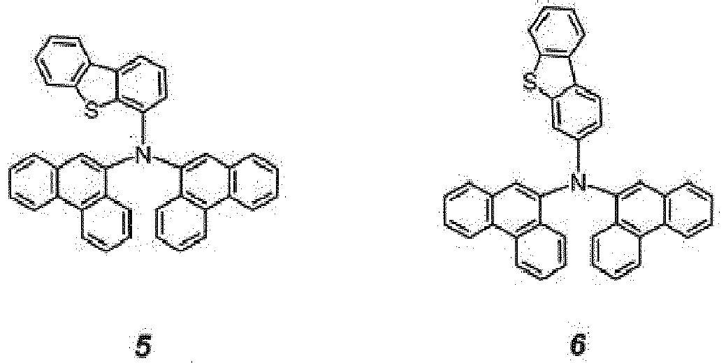
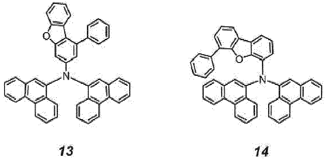
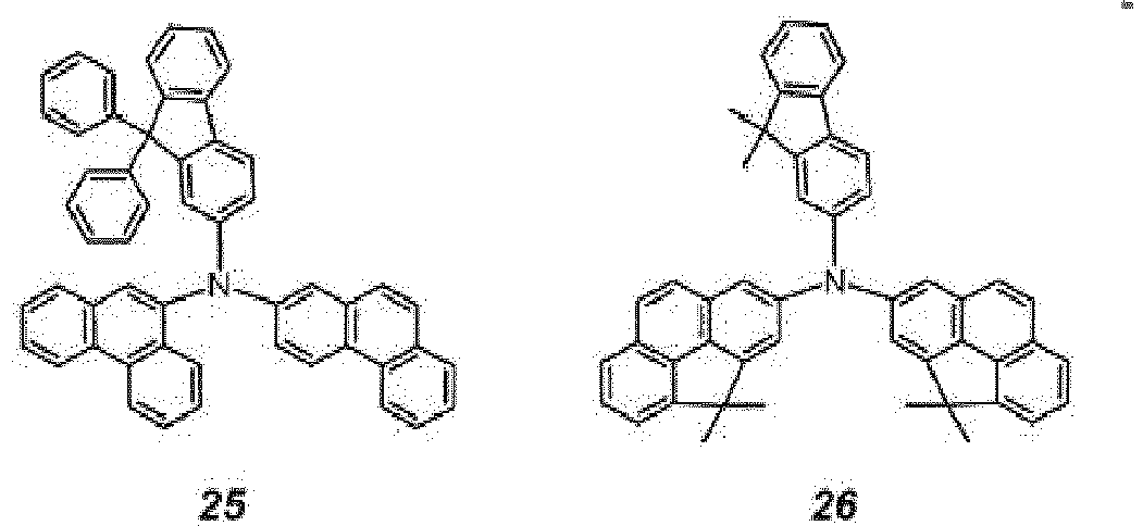
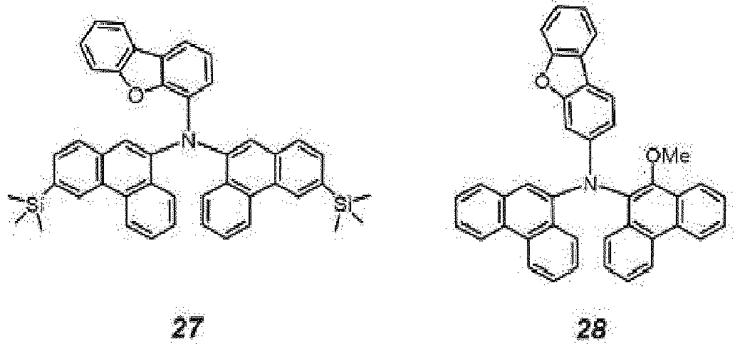
- the material for an organic EL device according to the present disclosure may be, for example, materials represented by the following structures.
- the monoamine material for an organic EL device according to the present disclosure introduces two phenanthryl parts to a monoamine, and the hole transport properties and electron tolerance thereof may be improved. Accordingly, by using the monoamine material for an organic EL device according to the present disclosure as a material for a layer present between an anode and an emission layer, an organic EL device having high efficiency and long life may be attained.
- the transfer of electrons which are not consumed in an emission layer but reached a layer disposed near an anode, may be inhibited, and accordingly, the monoamine material for an organic EL device according to the present disclosure is used as a material of a layer present between an anode and an emission layer, so as to restrain the deterioration due to electrons in the layer disposed near the anode and attain the increase of life of an organic EL device.
- the monoamine material for an organic EL device according to the present disclosure may be used as a material of at least one layer present between an anode and an emission layer in an organic EL device.
- the monoamine material for an organic EL device according to the present disclosure may preferably be used as a material of a hole transport layer.
- the material may preferably be used as a material of a layer disposed near an emission layer, and may particularly preferably be used as a material of a layer adjacent to the emission layer in the multilayer structure.
- the monoamine material for an organic EL device As a material of a layer near or adjacent to an emission layer among layers present between an anode and an emission layer, the diffusion of electrons not consumed in the emission layer, to a layer disposed near the anode may be effectively restrained. Therefore, the deterioration of a layer disposed near the anode due to electrons may decrease, and the increase of life of an organic EL device may be attained.
- FIG. 1 is a schematic diagram of an organic EL device 100 according to an embodiment of the present disclosure.
- An organic EL device 100 includes, for example, a substrate 102, an anode 104, a hole injection layer 106, a hole transport layer 108, an emission layer 110, an electron transport layer 112, an electron injection layer 114, and a cathode 116.
- the monoamine material for an organic EL device according to the present disclosure may be used in at least one layer of laminated layers disposed between an emission layer and an anode.
- the monoamine material for an organic EL device according to the present disclosure is used in the hole transport layer 108 will be explained, as an example.
- the substrate 102 may be, for example, a transparent glass substrate, a semiconductor substrate formed using silicon, etc., or a flexible substrate of a resin, etc.
- the anode (Anode) 104 is disposed on the substrate 102 and may be formed using indium tin oxide (ITO), indium zinc oxide (IZO), etc.
- the hole injection layer (HIL) 106 is disposed on the anode 104 and may include, for example, 4,4',4"-tris(N-1 -naphthyl-N-phenylamino)triphenylamine (1 -TNATA), 4,4' ,4"-tris(N-(2-naphthyl)-N-phenylamino)-triphenylamine (2-TNATA), 4,4-bis(N,N-di(3-tolyl)amino)-3,3-dimethylbiphenyl (HMTPD), etc.
- the hole transport layer (HTL) 108 is disposed on the hole injection layer 106 and is formed using the monoamine material for an organic EL device according to the present disclosure.
- the emission layer (EL) 110 is disposed on the hole transport layer 108 and may be formed by, for example, doping 9,10-di(2-naphthyl)anthracene (ADN) with tetra-t-butylperylene (TBP) .
- ADN 9,10-di(2-naphthyl)anthracene
- TBP tetra-t-butylperylene
- the electron transport layer (ETL) 112 is disposed on the emission layer 110 and is formed using, for example, a material including tris(8-hydroxyquinolinato)aluminum (Alq 3 ).
- the electron injection layer (EIL) 114 is disposed on the electron transport layer 112 and is formed by, for example, a material including lithium fluoride (LiF).
- the cathode (Cathode) 116 is disposed on the electron injection layer 114 and is formed by a metal such as Al or a transparent material such as ITO and IZO.
- the thin film may be formed by selecting an appropriate layer forming method such as a vacuum deposition method, a sputtering method, and various coating methods depending on the material used.
- the organic EL device 100 by using the monoamine material for an organic EL device according to the present disclosure, the deterioration of a layer present near an anode due to electrons may be restrained, and the increase of efficiency and life of the organic EL device 100 may be attained.
- the monoamine material for an organic EL device according to the present disclosure may be used as a material of a hole injection layer.
- the monoamine material for an organic EL device according to the present disclosure in at least one layer laminated between an emission layer and an anode, the increase of efficiency and life of an organic EL device may be attained.
- the monoamine material for an organic EL device according to the present disclosure may be applied to an organic EL light-emitting display of an active matrix type using a TFT.
- a TBP fluorescent material is used as a dopant material in an emission layer in the organic EL device 100
- a phosphorescent compound may be also used as a material of an emission layer in the organic EL device according to the present disclosure.
- a monoamine material for an organic EL device according to the present disclosure may be synthesized by reacting the following Compound 35 or an arylamine compound having a similar structure with a halogen compound of an aryl compound such as phenanthrene or a heteroaryl compound using a Pd catalyst, etc.
- the monoamine material for an organic EL device according to the present disclosure may be synthesized, for example, as follows.
- the identification of Compound 1 was conducted by detecting molecular ion peak in FAB-MS measurement.
- the molecular weight of Compound 1 measured by FAB-MS was 535.
- the monoamine material for an organic EL device according to the present disclosure may be synthesized, for example, as follows.
- the identification of Compound 2 was conducted by detecting molecular ion peak in FAB-MS measurement.
- the molecular weight of Compound 2 measured by FAB-MS was 535.
- the monoamine material for an organic EL device according to the present disclosure may be synthesized, for example, as follows.
- Compound 11 was obtained by performing the same synthetic method of Compound 9 except for using 2-bromo-9,9-diphenylfluorene instead of Compound 39.
- the monoamine material for an organic EL device according to the present disclosure may be synthesized, for example, as follows.
- the identification of Compound 13 was conducted by detecting molecular ion peak in FAB-MS measurement.
- the molecular weight of Compound 13 measured by FAB-MS was 612.
- Comparative Compound c1 to Comparative Compound c3 were prepared for comparison.
- Organic EL devices 200 were formed by a similar method for forming the organic EL device 100 and using Compound 2, Compound 9, Compound 11, or Comparative Compound c1 to Comparative Compound c3, as hole transport materials.
- a substrate 202 was formed using a transparent glass substrate, an anode 204 was formed using ITO to a layer thickness of about 150 nm, a hole injection layer 206 was formed using 2-TNATA to a layer thickness of about 60 nm, a hole transport layer 208 was formed to a layer thickness of about 30 nm, an emission layer 210 was formed by doping ADN with 3% TBP to a layer thickness of about 25 nm, an electron transport layer 212 was formed using Alq 3 to a layer thickness of about 25 nm, an electron injection layer 214 was formed using LiF to a layer thickness of about 1nm, and a cathode 216 was formed using Al to a layer thickness of about 100 nm.
- Example 2 when comparing Example 2 and Comparative Example 2 in which phenanthrene combined with an amine is replaced with pyrene, the improvement of emission efficiency and device life were recognized.
- Example 3 when comparing Example 2 with Example 3, Example 3 using a compound in which one of two phenanthryl groups is combined with the nitrogen atom (N) of an amine at position 9, and the other one is combined with the nitrogen atom (N) at position 2, that is, Compound 9 in which two phenanthryl groups are asymmetrically combined with the nitrogen atom (N) of an amine, has increased life when compared with Example 2.
- the monoamine material for an organic EL device according to the present disclosure has improved hole transport property and electron tolerance and may inhibit electron transfer by introducing two phenanthrene parts to the nitrogen atom of an amine.
- an organic EL device having high efficiency and long life may be attained by using a monoamine material for an organic EL device according to the present disclosure as a material for at least one layer present between an anode and an emission layer.
- a material for an organic EL device having high efficiency and long life, and an organic EL device using the same may be provided.
Landscapes
- Chemical & Material Sciences (AREA)
- Organic Chemistry (AREA)
- Engineering & Computer Science (AREA)
- Materials Engineering (AREA)
- Physics & Mathematics (AREA)
- Spectroscopy & Molecular Physics (AREA)
- Optics & Photonics (AREA)
- Electroluminescent Light Sources (AREA)
- Furan Compounds (AREA)
- Organic Low-Molecular-Weight Compounds And Preparation Thereof (AREA)
Claims (6)
- Matériau monoamine pour un dispositif électroluminescent (EL) organique, représenté par la formule générale (1) suivante :

- Matériau monoamine pour un dispositif EL organique selon la revendication 1, dans lequel un groupe phénanthryle dans la formule générale (1) est combiné à un atome d'azote en une position autre que la position 9 ou la position 10.
- Matériau monoamine pour un dispositif EL organique, représenté par la formule générale (2) suivante :

- Matériau monoamine pour un dispositif EL organique, où le matériau monoamine est choisi parmi les composés représentés par les structures suivantes :








- Dispositif électroluminescent (EL) organique comprenant le matériau pour un dispositif EL organique décrit dans l'une quelconque des revendications 1 à 4 dans au moins une couche stratifiée entre une couche d'émission et une anode.
- Dispositif électroluminescent (EL) organique selon la revendication 5, dans lequel le matériau pour un dispositif EL organique décrit dans l'une quelconque des revendications 1 à 4 est compris dans une couche stratifiée entre une couche d'émission et une anode, la couche étant adjacente à la couche d'émission.
Applications Claiming Priority (3)
| Application Number | Priority Date | Filing Date | Title |
|---|---|---|---|
| JP2014163347 | 2014-08-11 | ||
| JP2015156701A JP6788335B2 (ja) | 2014-08-11 | 2015-08-07 | 有機エレクトロルミネッセンス素子用モノアミン材料及びそれを用いた有機エレクトロルミネッセンス素子 |
| PCT/KR2015/008398 WO2016024792A1 (fr) | 2014-08-11 | 2015-08-11 | Composé monoamine pour élément électroluminescent organique et élément électroluminescent organique l'utilisant |
Publications (3)
| Publication Number | Publication Date |
|---|---|
| EP3135744A1 EP3135744A1 (fr) | 2017-03-01 |
| EP3135744A4 EP3135744A4 (fr) | 2018-01-17 |
| EP3135744B1 true EP3135744B1 (fr) | 2021-09-29 |
Family
ID=55304360
Family Applications (1)
| Application Number | Title | Priority Date | Filing Date |
|---|---|---|---|
| EP15832353.5A Active EP3135744B1 (fr) | 2014-08-11 | 2015-08-11 | Composé monoamine pour élément électroluminescent organique et élément électroluminescent organique l'utilisant |
Country Status (6)
| Country | Link |
|---|---|
| US (1) | US10930854B2 (fr) |
| EP (1) | EP3135744B1 (fr) |
| JP (1) | JP6788335B2 (fr) |
| KR (1) | KR102374031B1 (fr) |
| CN (1) | CN106660985B (fr) |
| WO (1) | WO2016024792A1 (fr) |
Families Citing this family (7)
| Publication number | Priority date | Publication date | Assignee | Title |
|---|---|---|---|---|
| JP6879559B2 (ja) * | 2015-07-31 | 2021-06-02 | 出光興産株式会社 | 化合物、有機エレクトロルミネッセンス素子用材料、有機エレクトロルミネッセンス素子、及び電子機器 |
| JP6819964B2 (ja) * | 2015-07-31 | 2021-01-27 | 出光興産株式会社 | 化合物、有機エレクトロルミネッセンス素子用材料、有機エレクトロルミネッセンス素子、及び電子機器 |
| WO2017022727A1 (fr) * | 2015-07-31 | 2017-02-09 | 出光興産株式会社 | Composé, matériau pour éléments électroluminescents organiques, éléments électroluminescents organiques et dispositif électronique |
| EP3312166B1 (fr) | 2016-10-21 | 2019-11-27 | Samsung Display Co., Ltd. | Composé de monoamine et dispositif électroluminescent organique l'incluant |
| US20210399224A1 (en) * | 2018-11-29 | 2021-12-23 | Hodogaya Chemical Co., Ltd. | Organic electroluminescence element |
| KR20220034301A (ko) | 2020-09-10 | 2022-03-18 | 삼성디스플레이 주식회사 | 발광 소자 및 발광 소자용 모노 아민 화합물 |
| CN116283859B (zh) * | 2021-12-21 | 2025-04-25 | 广州华睿光电材料有限公司 | 有机化合物及包括其的混合物、组合物和有机电子器件 |
Family Cites Families (31)
| Publication number | Priority date | Publication date | Assignee | Title |
|---|---|---|---|---|
| US4720432A (en) | 1987-02-11 | 1988-01-19 | Eastman Kodak Company | Electroluminescent device with organic luminescent medium |
| JPH02178666A (ja) | 1988-12-29 | 1990-07-11 | Canon Inc | 電子写真感光体 |
| JP2000178666A (ja) | 1998-12-14 | 2000-06-27 | Shin Etsu Chem Co Ltd | 希土類金属の切削片屑の回収方法 |
| US6929872B2 (en) | 2000-10-05 | 2005-08-16 | Nippon Steel Chemical Co., Ltd. | Organic electroluminescent devices |
| JP4770033B2 (ja) | 2001-02-13 | 2011-09-07 | コニカミノルタホールディングス株式会社 | 有機エレクトロルミネッセンス素子 |
| JP2004262761A (ja) | 2003-01-16 | 2004-09-24 | Idemitsu Kosan Co Ltd | 芳香族アミン誘導体及びそれを用いた有機エレクトロルミネッセンス素子 |
| JP4152761B2 (ja) | 2003-01-29 | 2008-09-17 | 出光興産株式会社 | 芳香族アミン誘導体及びそれを用いた有機エレクトロルミネッセンス素子 |
| JP4177707B2 (ja) * | 2003-03-27 | 2008-11-05 | 三井化学株式会社 | アミン化合物および該化合物を含有する有機電界発光素子 |
| KR20050015902A (ko) | 2003-08-14 | 2005-02-21 | 엘지전자 주식회사 | 유기 el 소자 및 그 제조방법 |
| JP4653061B2 (ja) | 2005-12-20 | 2011-03-16 | キヤノン株式会社 | アミン化合物および有機発光素子および青色有機発光素子 |
| JP5064482B2 (ja) | 2006-03-14 | 2012-10-31 | エルジー・ケム・リミテッド | 高効率の有機発光素子およびその製造方法 |
| KR100974562B1 (ko) | 2007-12-31 | 2010-08-06 | 다우어드밴스드디스플레이머티리얼 유한회사 | 신규한 유기 발광 화합물 및 이를 발광재료로서 채용하고있는 유기 발광 소자 |
| KR20100007639A (ko) * | 2008-07-14 | 2010-01-22 | 덕산하이메탈(주) | 신규한 페닐-플루오렌 유도체 및 이를 포함하는 유기전계발광 소자 |
| WO2010041872A2 (fr) | 2008-10-08 | 2010-04-15 | 주식회사 엘지화학 | Nouveau composé et dispositif électronique organique l'utilisant |
| KR20100041043A (ko) | 2008-10-13 | 2010-04-22 | 다우어드밴스드디스플레이머티리얼 유한회사 | 신규한 유기 발광 화합물 및 이를 발광재료로서 채용하고 있는 유기 발광 소자 |
| KR20100048210A (ko) | 2008-10-30 | 2010-05-11 | 다우어드밴스드디스플레이머티리얼 유한회사 | 신규한 유기 발광 화합물 및 이를 포함하는 유기 발광 소자 |
| WO2010061824A1 (fr) | 2008-11-25 | 2010-06-03 | 出光興産株式会社 | Dérivé d'amine aromatique et élément électroluminescent organique |
| KR101557362B1 (ko) | 2008-12-31 | 2015-10-08 | 서울바이오시스 주식회사 | 복수개의 비극성 발광셀들을 갖는 발광 소자 및 그것을 제조하는 방법 |
| WO2010106806A1 (fr) | 2009-03-19 | 2010-09-23 | 三井化学株式会社 | Dérivé d'amine aromatique et élément électroluminescent organique l'utilisant |
| US9650565B2 (en) | 2009-10-20 | 2017-05-16 | Tosoh Corporation | Carbazole compound and use thereof |
| KR101097339B1 (ko) | 2010-03-08 | 2011-12-23 | 삼성모바일디스플레이주식회사 | 유기 발광 소자 및 이의 제조 방법 |
| EP2415769B1 (fr) | 2010-04-20 | 2015-10-28 | Idemitsu Kosan Co., Ltd. | Dérivé de bis-carbazole, matériau pour élément électroluminescent organique, et élément électroluminescent organique l'utilisant |
| KR20130007159A (ko) | 2011-06-29 | 2013-01-18 | 삼성디스플레이 주식회사 | 유기 발광 소자 |
| KR20130022232A (ko) * | 2011-08-25 | 2013-03-06 | 덕산하이메탈(주) | 유기전기소자용 신규 화합물, 이를 이용하는 유기전기소자 및 그 전자 장치 |
| WO2013118847A1 (fr) | 2012-02-10 | 2013-08-15 | 出光興産株式会社 | Dérivé d'amine aromatique, élément électroluminescent organique et dispositif électronique |
| WO2013118846A1 (fr) | 2012-02-10 | 2013-08-15 | 出光興産株式会社 | Dérivé d'amine aromatique, élément électroluminescent organique et dispositif électronique |
| DE102012011335A1 (de) * | 2012-06-06 | 2013-12-12 | Merck Patent Gmbh | Verbindungen für Organische Elekronische Vorrichtungen |
| CN102850334A (zh) * | 2012-08-28 | 2013-01-02 | 李崇 | 一种以二苯并呋喃为核心骨架的衍生物化合物及其在oled上的应用 |
| CN105378964B (zh) | 2013-07-12 | 2018-01-09 | 保土谷化学工业株式会社 | 有机电致发光器件 |
| KR101389527B1 (ko) * | 2013-09-17 | 2014-04-25 | 덕산하이메탈(주) | 유기전기 소자용 화합물을 이용한 유기전기소자 및 그 전자 장치 |
| JP6591433B2 (ja) * | 2014-03-07 | 2019-10-16 | メルク パテント ゲーエムベーハー | 電子素子のための材料 |
-
2015
- 2015-08-07 JP JP2015156701A patent/JP6788335B2/ja active Active
- 2015-08-11 US US15/322,292 patent/US10930854B2/en active Active
- 2015-08-11 CN CN201580037766.XA patent/CN106660985B/zh active Active
- 2015-08-11 KR KR1020167033174A patent/KR102374031B1/ko active Active
- 2015-08-11 WO PCT/KR2015/008398 patent/WO2016024792A1/fr not_active Ceased
- 2015-08-11 EP EP15832353.5A patent/EP3135744B1/fr active Active
Also Published As
| Publication number | Publication date |
|---|---|
| EP3135744A1 (fr) | 2017-03-01 |
| JP2016040824A (ja) | 2016-03-24 |
| JP6788335B2 (ja) | 2020-11-25 |
| CN106660985B (zh) | 2019-12-17 |
| US20170133591A1 (en) | 2017-05-11 |
| EP3135744A4 (fr) | 2018-01-17 |
| KR20170043099A (ko) | 2017-04-20 |
| WO2016024792A1 (fr) | 2016-02-18 |
| US10930854B2 (en) | 2021-02-23 |
| KR102374031B1 (ko) | 2022-03-15 |
| CN106660985A (zh) | 2017-05-10 |
Similar Documents
| Publication | Publication Date | Title |
|---|---|---|
| EP3135744B1 (fr) | Composé monoamine pour élément électroluminescent organique et élément électroluminescent organique l'utilisant | |
| JP6424002B2 (ja) | 有機エレクトロルミネッセンス素子および有機エレクトロルミネッセンス素子用材料 | |
| EP2713415B1 (fr) | Matériau pour élément électroluminescent organique, et élément électroluminescent organique | |
| EP2338186B1 (fr) | Dispositif électroluminescent organique et matériaux pour une utilisation dans celui-ci | |
| EP2085371B1 (fr) | Composé de fluoranthène, dispositif électroluminescent organique utilisant le composé de fluoranthène et solution contenant un matériau électroluminescent organique | |
| CN107556298B (zh) | 芳香族杂环衍生物、有机电致发光元件用材料以及有机电致发光元件 | |
| EP2166587A1 (fr) | Dispositif électroluminescent organique et matériau pour un dispositif électroluminescent organique | |
| US20160365516A1 (en) | Ink composition, organic electroluminescence element, and electronic apparatus | |
| EP2133932A1 (fr) | Dispositif électroluminescent organique | |
| EP2415769A1 (fr) | Dérivé de bis-carbazole, matériau pour élément électroluminescent organique, et élément électroluminescent organique l'utilisant | |
| EP2166592A1 (fr) | Dispositif électroluminescent organique | |
| EP2166591A1 (fr) | Dispositif électroluminescent organique | |
| KR20160019839A (ko) | 유기 일렉트로루미네센스 소자용 모노아민 재료 및 이를 사용한 유기 일렉트로루미네센스 소자 | |
| KR20130018725A (ko) | 유기 전기발광 소자용 재료 및 그것을 이용한 유기 전기발광 소자 | |
| WO2013058343A1 (fr) | Élément à électroluminescence organique et matériau pour élément à électroluminescence organique | |
| WO2013146942A1 (fr) | Nouveau composé, matériau pour élément électroluminescent organique, et élément électroluminescent organique | |
| US9650519B2 (en) | Ink composition, organic electroluminescence element, and electronic apparatus | |
| JP2014531747A (ja) | 新規有機エレクトロルミネッセンス化合物およびこれを使用した有機エレクトロルミネッセンス素子 | |
| KR101554680B1 (ko) | 방향족 아민 화합물 및 이를 포함하는 유기전계 발광소자 | |
| EP2645443A1 (fr) | Élément électroluminescent organique | |
| EP1933396A1 (fr) | Element organique electroluminescent utilisant une polyarylamine | |
| KR20150071640A (ko) | 유기 일렉트로루미네센스 소자용 재료 및 그것을 포함하는 유기 일렉트로루미네센스 소자 | |
| Kim et al. | New ambipolar blue emitting materials based on amino coumarin derivatives with high efficiency for organic lightemitting diodes | |
| US20150263298A1 (en) | Silane compound and organic electroluminescence device` | |
| CN112390811B (zh) | 一种双硫杂蒽酮类衍生物及其制备方法和应用 |
Legal Events
| Date | Code | Title | Description |
|---|---|---|---|
| STAA | Information on the status of an ep patent application or granted ep patent |
Free format text: STATUS: THE INTERNATIONAL PUBLICATION HAS BEEN MADE |
|
| PUAI | Public reference made under article 153(3) epc to a published international application that has entered the european phase |
Free format text: ORIGINAL CODE: 0009012 |
|
| STAA | Information on the status of an ep patent application or granted ep patent |
Free format text: STATUS: REQUEST FOR EXAMINATION WAS MADE |
|
| 17P | Request for examination filed |
Effective date: 20161123 |
|
| AK | Designated contracting states |
Kind code of ref document: A1 Designated state(s): AL AT BE BG CH CY CZ DE DK EE ES FI FR GB GR HR HU IE IS IT LI LT LU LV MC MK MT NL NO PL PT RO RS SE SI SK SM TR |
|
| AX | Request for extension of the european patent |
Extension state: BA ME |
|
| DAV | Request for validation of the european patent (deleted) | ||
| DAX | Request for extension of the european patent (deleted) | ||
| RIC1 | Information provided on ipc code assigned before grant |
Ipc: C07D 307/91 20060101ALI20171207BHEP Ipc: C07D 333/76 20060101ALI20171207BHEP Ipc: C09K 11/06 20060101AFI20171207BHEP Ipc: H01L 51/50 20060101ALI20171207BHEP |
|
| A4 | Supplementary search report drawn up and despatched |
Effective date: 20171215 |
|
| STAA | Information on the status of an ep patent application or granted ep patent |
Free format text: STATUS: EXAMINATION IS IN PROGRESS |
|
| 17Q | First examination report despatched |
Effective date: 20190521 |
|
| GRAP | Despatch of communication of intention to grant a patent |
Free format text: ORIGINAL CODE: EPIDOSNIGR1 |
|
| STAA | Information on the status of an ep patent application or granted ep patent |
Free format text: STATUS: GRANT OF PATENT IS INTENDED |
|
| INTG | Intention to grant announced |
Effective date: 20210429 |
|
| GRAS | Grant fee paid |
Free format text: ORIGINAL CODE: EPIDOSNIGR3 |
|
| GRAA | (expected) grant |
Free format text: ORIGINAL CODE: 0009210 |
|
| STAA | Information on the status of an ep patent application or granted ep patent |
Free format text: STATUS: THE PATENT HAS BEEN GRANTED |
|
| AK | Designated contracting states |
Kind code of ref document: B1 Designated state(s): AL AT BE BG CH CY CZ DE DK EE ES FI FR GB GR HR HU IE IS IT LI LT LU LV MC MK MT NL NO PL PT RO RS SE SI SK SM TR |
|
| REG | Reference to a national code |
Ref country code: GB Ref legal event code: FG4D |
|
| REG | Reference to a national code |
Ref country code: CH Ref legal event code: EP Ref country code: AT Ref legal event code: REF Ref document number: 1434202 Country of ref document: AT Kind code of ref document: T Effective date: 20211015 |
|
| REG | Reference to a national code |
Ref country code: DE Ref legal event code: R096 Ref document number: 602015073759 Country of ref document: DE |
|
| REG | Reference to a national code |
Ref country code: IE Ref legal event code: FG4D |
|
| REG | Reference to a national code |
Ref country code: LT Ref legal event code: MG9D |
|
| PG25 | Lapsed in a contracting state [announced via postgrant information from national office to epo] |
Ref country code: LT Free format text: LAPSE BECAUSE OF FAILURE TO SUBMIT A TRANSLATION OF THE DESCRIPTION OR TO PAY THE FEE WITHIN THE PRESCRIBED TIME-LIMIT Effective date: 20210929 Ref country code: BG Free format text: LAPSE BECAUSE OF FAILURE TO SUBMIT A TRANSLATION OF THE DESCRIPTION OR TO PAY THE FEE WITHIN THE PRESCRIBED TIME-LIMIT Effective date: 20211229 Ref country code: FI Free format text: LAPSE BECAUSE OF FAILURE TO SUBMIT A TRANSLATION OF THE DESCRIPTION OR TO PAY THE FEE WITHIN THE PRESCRIBED TIME-LIMIT Effective date: 20210929 Ref country code: NO Free format text: LAPSE BECAUSE OF FAILURE TO SUBMIT A TRANSLATION OF THE DESCRIPTION OR TO PAY THE FEE WITHIN THE PRESCRIBED TIME-LIMIT Effective date: 20211229 Ref country code: HR Free format text: LAPSE BECAUSE OF FAILURE TO SUBMIT A TRANSLATION OF THE DESCRIPTION OR TO PAY THE FEE WITHIN THE PRESCRIBED TIME-LIMIT Effective date: 20210929 Ref country code: RS Free format text: LAPSE BECAUSE OF FAILURE TO SUBMIT A TRANSLATION OF THE DESCRIPTION OR TO PAY THE FEE WITHIN THE PRESCRIBED TIME-LIMIT Effective date: 20210929 Ref country code: SE Free format text: LAPSE BECAUSE OF FAILURE TO SUBMIT A TRANSLATION OF THE DESCRIPTION OR TO PAY THE FEE WITHIN THE PRESCRIBED TIME-LIMIT Effective date: 20210929 |
|
| REG | Reference to a national code |
Ref country code: NL Ref legal event code: MP Effective date: 20210929 |
|
| REG | Reference to a national code |
Ref country code: AT Ref legal event code: MK05 Ref document number: 1434202 Country of ref document: AT Kind code of ref document: T Effective date: 20210929 |
|
| PG25 | Lapsed in a contracting state [announced via postgrant information from national office to epo] |
Ref country code: LV Free format text: LAPSE BECAUSE OF FAILURE TO SUBMIT A TRANSLATION OF THE DESCRIPTION OR TO PAY THE FEE WITHIN THE PRESCRIBED TIME-LIMIT Effective date: 20210929 Ref country code: GR Free format text: LAPSE BECAUSE OF FAILURE TO SUBMIT A TRANSLATION OF THE DESCRIPTION OR TO PAY THE FEE WITHIN THE PRESCRIBED TIME-LIMIT Effective date: 20211230 |
|
| PG25 | Lapsed in a contracting state [announced via postgrant information from national office to epo] |
Ref country code: AT Free format text: LAPSE BECAUSE OF FAILURE TO SUBMIT A TRANSLATION OF THE DESCRIPTION OR TO PAY THE FEE WITHIN THE PRESCRIBED TIME-LIMIT Effective date: 20210929 |
|
| PG25 | Lapsed in a contracting state [announced via postgrant information from national office to epo] |
Ref country code: IS Free format text: LAPSE BECAUSE OF FAILURE TO SUBMIT A TRANSLATION OF THE DESCRIPTION OR TO PAY THE FEE WITHIN THE PRESCRIBED TIME-LIMIT Effective date: 20220129 Ref country code: SK Free format text: LAPSE BECAUSE OF FAILURE TO SUBMIT A TRANSLATION OF THE DESCRIPTION OR TO PAY THE FEE WITHIN THE PRESCRIBED TIME-LIMIT Effective date: 20210929 Ref country code: RO Free format text: LAPSE BECAUSE OF FAILURE TO SUBMIT A TRANSLATION OF THE DESCRIPTION OR TO PAY THE FEE WITHIN THE PRESCRIBED TIME-LIMIT Effective date: 20210929 Ref country code: PT Free format text: LAPSE BECAUSE OF FAILURE TO SUBMIT A TRANSLATION OF THE DESCRIPTION OR TO PAY THE FEE WITHIN THE PRESCRIBED TIME-LIMIT Effective date: 20220131 Ref country code: PL Free format text: LAPSE BECAUSE OF FAILURE TO SUBMIT A TRANSLATION OF THE DESCRIPTION OR TO PAY THE FEE WITHIN THE PRESCRIBED TIME-LIMIT Effective date: 20210929 Ref country code: NL Free format text: LAPSE BECAUSE OF FAILURE TO SUBMIT A TRANSLATION OF THE DESCRIPTION OR TO PAY THE FEE WITHIN THE PRESCRIBED TIME-LIMIT Effective date: 20210929 Ref country code: ES Free format text: LAPSE BECAUSE OF FAILURE TO SUBMIT A TRANSLATION OF THE DESCRIPTION OR TO PAY THE FEE WITHIN THE PRESCRIBED TIME-LIMIT Effective date: 20210929 Ref country code: EE Free format text: LAPSE BECAUSE OF FAILURE TO SUBMIT A TRANSLATION OF THE DESCRIPTION OR TO PAY THE FEE WITHIN THE PRESCRIBED TIME-LIMIT Effective date: 20210929 Ref country code: CZ Free format text: LAPSE BECAUSE OF FAILURE TO SUBMIT A TRANSLATION OF THE DESCRIPTION OR TO PAY THE FEE WITHIN THE PRESCRIBED TIME-LIMIT Effective date: 20210929 Ref country code: AL Free format text: LAPSE BECAUSE OF FAILURE TO SUBMIT A TRANSLATION OF THE DESCRIPTION OR TO PAY THE FEE WITHIN THE PRESCRIBED TIME-LIMIT Effective date: 20210929 |
|
| REG | Reference to a national code |
Ref country code: DE Ref legal event code: R097 Ref document number: 602015073759 Country of ref document: DE |
|
| PG25 | Lapsed in a contracting state [announced via postgrant information from national office to epo] |
Ref country code: DK Free format text: LAPSE BECAUSE OF FAILURE TO SUBMIT A TRANSLATION OF THE DESCRIPTION OR TO PAY THE FEE WITHIN THE PRESCRIBED TIME-LIMIT Effective date: 20210929 |
|
| PLBE | No opposition filed within time limit |
Free format text: ORIGINAL CODE: 0009261 |
|
| STAA | Information on the status of an ep patent application or granted ep patent |
Free format text: STATUS: NO OPPOSITION FILED WITHIN TIME LIMIT |
|
| 26N | No opposition filed |
Effective date: 20220630 |
|
| PG25 | Lapsed in a contracting state [announced via postgrant information from national office to epo] |
Ref country code: SI Free format text: LAPSE BECAUSE OF FAILURE TO SUBMIT A TRANSLATION OF THE DESCRIPTION OR TO PAY THE FEE WITHIN THE PRESCRIBED TIME-LIMIT Effective date: 20210929 |
|
| PG25 | Lapsed in a contracting state [announced via postgrant information from national office to epo] |
Ref country code: IT Free format text: LAPSE BECAUSE OF FAILURE TO SUBMIT A TRANSLATION OF THE DESCRIPTION OR TO PAY THE FEE WITHIN THE PRESCRIBED TIME-LIMIT Effective date: 20210929 |
|
| PG25 | Lapsed in a contracting state [announced via postgrant information from national office to epo] |
Ref country code: MC Free format text: LAPSE BECAUSE OF FAILURE TO SUBMIT A TRANSLATION OF THE DESCRIPTION OR TO PAY THE FEE WITHIN THE PRESCRIBED TIME-LIMIT Effective date: 20210929 |
|
| REG | Reference to a national code |
Ref country code: CH Ref legal event code: PL |
|
| PG25 | Lapsed in a contracting state [announced via postgrant information from national office to epo] |
Ref country code: LU Free format text: LAPSE BECAUSE OF NON-PAYMENT OF DUE FEES Effective date: 20220811 Ref country code: LI Free format text: LAPSE BECAUSE OF NON-PAYMENT OF DUE FEES Effective date: 20220831 Ref country code: CH Free format text: LAPSE BECAUSE OF NON-PAYMENT OF DUE FEES Effective date: 20220831 |
|
| REG | Reference to a national code |
Ref country code: BE Ref legal event code: MM Effective date: 20220831 |
|
| P01 | Opt-out of the competence of the unified patent court (upc) registered |
Effective date: 20230516 |
|
| PG25 | Lapsed in a contracting state [announced via postgrant information from national office to epo] |
Ref country code: IE Free format text: LAPSE BECAUSE OF NON-PAYMENT OF DUE FEES Effective date: 20220811 |
|
| PG25 | Lapsed in a contracting state [announced via postgrant information from national office to epo] |
Ref country code: BE Free format text: LAPSE BECAUSE OF NON-PAYMENT OF DUE FEES Effective date: 20220831 |
|
| PG25 | Lapsed in a contracting state [announced via postgrant information from national office to epo] |
Ref country code: HU Free format text: LAPSE BECAUSE OF FAILURE TO SUBMIT A TRANSLATION OF THE DESCRIPTION OR TO PAY THE FEE WITHIN THE PRESCRIBED TIME-LIMIT; INVALID AB INITIO Effective date: 20150811 |
|
| PG25 | Lapsed in a contracting state [announced via postgrant information from national office to epo] |
Ref country code: SM Free format text: LAPSE BECAUSE OF FAILURE TO SUBMIT A TRANSLATION OF THE DESCRIPTION OR TO PAY THE FEE WITHIN THE PRESCRIBED TIME-LIMIT Effective date: 20210929 Ref country code: CY Free format text: LAPSE BECAUSE OF FAILURE TO SUBMIT A TRANSLATION OF THE DESCRIPTION OR TO PAY THE FEE WITHIN THE PRESCRIBED TIME-LIMIT Effective date: 20210929 |
|
| PG25 | Lapsed in a contracting state [announced via postgrant information from national office to epo] |
Ref country code: MK Free format text: LAPSE BECAUSE OF FAILURE TO SUBMIT A TRANSLATION OF THE DESCRIPTION OR TO PAY THE FEE WITHIN THE PRESCRIBED TIME-LIMIT Effective date: 20210929 |
|
| PG25 | Lapsed in a contracting state [announced via postgrant information from national office to epo] |
Ref country code: MT Free format text: LAPSE BECAUSE OF FAILURE TO SUBMIT A TRANSLATION OF THE DESCRIPTION OR TO PAY THE FEE WITHIN THE PRESCRIBED TIME-LIMIT Effective date: 20210929 |
|
| PGFP | Annual fee paid to national office [announced via postgrant information from national office to epo] |
Ref country code: DE Payment date: 20250721 Year of fee payment: 11 |
|
| PGFP | Annual fee paid to national office [announced via postgrant information from national office to epo] |
Ref country code: GB Payment date: 20250722 Year of fee payment: 11 |
|
| PGFP | Annual fee paid to national office [announced via postgrant information from national office to epo] |
Ref country code: FR Payment date: 20250725 Year of fee payment: 11 |
|
| PG25 | Lapsed in a contracting state [announced via postgrant information from national office to epo] |
Ref country code: TR Free format text: LAPSE BECAUSE OF FAILURE TO SUBMIT A TRANSLATION OF THE DESCRIPTION OR TO PAY THE FEE WITHIN THE PRESCRIBED TIME-LIMIT Effective date: 20210929 |