EP3141878B1 - Dispositif et procédé de fonctionnement de capteurs à infrarouge passif - Google Patents
Dispositif et procédé de fonctionnement de capteurs à infrarouge passif Download PDFInfo
- Publication number
- EP3141878B1 EP3141878B1 EP16192823.9A EP16192823A EP3141878B1 EP 3141878 B1 EP3141878 B1 EP 3141878B1 EP 16192823 A EP16192823 A EP 16192823A EP 3141878 B1 EP3141878 B1 EP 3141878B1
- Authority
- EP
- European Patent Office
- Prior art keywords
- digital
- pir
- current
- current source
- comparator
- Prior art date
- Legal status (The legal status is an assumption and is not a legal conclusion. Google has not performed a legal analysis and makes no representation as to the accuracy of the status listed.)
- Active
Links
Images






Classifications
-
- C—CHEMISTRY; METALLURGY
- C12—BIOCHEMISTRY; BEER; SPIRITS; WINE; VINEGAR; MICROBIOLOGY; ENZYMOLOGY; MUTATION OR GENETIC ENGINEERING
- C12G—WINE; PREPARATION THEREOF; ALCOHOLIC BEVERAGES; PREPARATION OF ALCOHOLIC BEVERAGES NOT PROVIDED FOR IN SUBCLASSES C12C OR C12H
- C12G3/00—Preparation of other alcoholic beverages
-
- G—PHYSICS
- G01—MEASURING; TESTING
- G01J—MEASUREMENT OF INTENSITY, VELOCITY, SPECTRAL CONTENT, POLARISATION, PHASE OR PULSE CHARACTERISTICS OF INFRARED, VISIBLE OR ULTRAVIOLET LIGHT; COLORIMETRY; RADIATION PYROMETRY
- G01J5/00—Radiation pyrometry, e.g. infrared or optical thermometry
- G01J5/10—Radiation pyrometry, e.g. infrared or optical thermometry using electric radiation detectors
-
- A—HUMAN NECESSITIES
- A23—FOODS OR FOODSTUFFS; TREATMENT THEREOF, NOT COVERED BY OTHER CLASSES
- A23L—FOODS, FOODSTUFFS OR NON-ALCOHOLIC BEVERAGES, NOT OTHERWISE PROVIDED FOR; PREPARATION OR TREATMENT THEREOF
- A23L7/00—Cereal-derived products; Malt products; Preparation or treatment thereof
- A23L7/20—Malt products
- A23L7/25—Fermentation of cereal malt or of cereal by malting
-
- C—CHEMISTRY; METALLURGY
- C12—BIOCHEMISTRY; BEER; SPIRITS; WINE; VINEGAR; MICROBIOLOGY; ENZYMOLOGY; MUTATION OR GENETIC ENGINEERING
- C12C—BEER; PREPARATION OF BEER BY FERMENTATION; PREPARATION OF MALT FOR MAKING BEER; PREPARATION OF HOPS FOR MAKING BEER
- C12C7/00—Preparation of wort
- C12C7/14—Lautering, i.e. clarifying wort
- C12C7/16—Lautering, i.e. clarifying wort by straining
- C12C7/163—Lautering, i.e. clarifying wort by straining with transport of the mash by or relative to a filtering surface
-
- C—CHEMISTRY; METALLURGY
- C12—BIOCHEMISTRY; BEER; SPIRITS; WINE; VINEGAR; MICROBIOLOGY; ENZYMOLOGY; MUTATION OR GENETIC ENGINEERING
- C12C—BEER; PREPARATION OF BEER BY FERMENTATION; PREPARATION OF MALT FOR MAKING BEER; PREPARATION OF HOPS FOR MAKING BEER
- C12C7/00—Preparation of wort
- C12C7/28—After-treatment, e.g. sterilisation
- C12C7/282—Concentration or beerwort
-
- G—PHYSICS
- G01—MEASURING; TESTING
- G01J—MEASUREMENT OF INTENSITY, VELOCITY, SPECTRAL CONTENT, POLARISATION, PHASE OR PULSE CHARACTERISTICS OF INFRARED, VISIBLE OR ULTRAVIOLET LIGHT; COLORIMETRY; RADIATION PYROMETRY
- G01J1/00—Photometry, e.g. photographic exposure meter
- G01J1/42—Photometry, e.g. photographic exposure meter using electric radiation detectors
- G01J1/44—Electric circuits
- G01J1/46—Electric circuits using a capacitor
-
- G—PHYSICS
- G01—MEASURING; TESTING
- G01J—MEASUREMENT OF INTENSITY, VELOCITY, SPECTRAL CONTENT, POLARISATION, PHASE OR PULSE CHARACTERISTICS OF INFRARED, VISIBLE OR ULTRAVIOLET LIGHT; COLORIMETRY; RADIATION PYROMETRY
- G01J5/00—Radiation pyrometry, e.g. infrared or optical thermometry
- G01J5/10—Radiation pyrometry, e.g. infrared or optical thermometry using electric radiation detectors
- G01J5/12—Radiation pyrometry, e.g. infrared or optical thermometry using electric radiation detectors using thermoelectric elements, e.g. thermocouples
- G01J5/14—Electrical features thereof
-
- G—PHYSICS
- G01—MEASURING; TESTING
- G01J—MEASUREMENT OF INTENSITY, VELOCITY, SPECTRAL CONTENT, POLARISATION, PHASE OR PULSE CHARACTERISTICS OF INFRARED, VISIBLE OR ULTRAVIOLET LIGHT; COLORIMETRY; RADIATION PYROMETRY
- G01J5/00—Radiation pyrometry, e.g. infrared or optical thermometry
- G01J5/10—Radiation pyrometry, e.g. infrared or optical thermometry using electric radiation detectors
- G01J5/20—Radiation pyrometry, e.g. infrared or optical thermometry using electric radiation detectors using resistors, thermistors or semiconductors sensitive to radiation, e.g. photoconductive devices
- G01J5/22—Electrical features thereof
- G01J5/24—Use of specially adapted circuits, e.g. bridge circuits
-
- G—PHYSICS
- G08—SIGNALLING
- G08B—SIGNALLING SYSTEMS, e.g. PERSONAL CALLING SYSTEMS; ORDER TELEGRAPHS; ALARM SYSTEMS
- G08B13/00—Burglar, theft or intruder alarms
- G08B13/18—Actuation by interference with heat, light, or radiation of shorter wavelength; Actuation by intruding sources of heat, light, or radiation of shorter wavelength
- G08B13/189—Actuation by interference with heat, light, or radiation of shorter wavelength; Actuation by intruding sources of heat, light, or radiation of shorter wavelength using passive radiation detection systems
- G08B13/19—Actuation by interference with heat, light, or radiation of shorter wavelength; Actuation by intruding sources of heat, light, or radiation of shorter wavelength using passive radiation detection systems using infrared-radiation detection systems
- G08B13/191—Actuation by interference with heat, light, or radiation of shorter wavelength; Actuation by intruding sources of heat, light, or radiation of shorter wavelength using passive radiation detection systems using infrared-radiation detection systems using pyroelectric sensor means
-
- H—ELECTRICITY
- H03—ELECTRONIC CIRCUITRY
- H03M—CODING; DECODING; CODE CONVERSION IN GENERAL
- H03M1/00—Analogue/digital conversion; Digital/analogue conversion
- H03M1/12—Analogue/digital converters
-
- G—PHYSICS
- G08—SIGNALLING
- G08B—SIGNALLING SYSTEMS, e.g. PERSONAL CALLING SYSTEMS; ORDER TELEGRAPHS; ALARM SYSTEMS
- G08B13/00—Burglar, theft or intruder alarms
- G08B13/18—Actuation by interference with heat, light, or radiation of shorter wavelength; Actuation by intruding sources of heat, light, or radiation of shorter wavelength
- G08B13/189—Actuation by interference with heat, light, or radiation of shorter wavelength; Actuation by intruding sources of heat, light, or radiation of shorter wavelength using passive radiation detection systems
- G08B13/19—Actuation by interference with heat, light, or radiation of shorter wavelength; Actuation by intruding sources of heat, light, or radiation of shorter wavelength using passive radiation detection systems using infrared-radiation detection systems
-
- H—ELECTRICITY
- H03—ELECTRONIC CIRCUITRY
- H03B—GENERATION OF OSCILLATIONS, DIRECTLY OR BY FREQUENCY-CHANGING, BY CIRCUITS EMPLOYING ACTIVE ELEMENTS WHICH OPERATE IN A NON-SWITCHING MANNER; GENERATION OF NOISE BY SUCH CIRCUITS
- H03B5/00—Generation of oscillations using amplifier with regenerative feedback from output to input
- H03B5/08—Generation of oscillations using amplifier with regenerative feedback from output to input with frequency-determining element comprising lumped inductance and capacitance
- H03B5/12—Generation of oscillations using amplifier with regenerative feedback from output to input with frequency-determining element comprising lumped inductance and capacitance active element in amplifier being semiconductor device
- H03B5/1206—Generation of oscillations using amplifier with regenerative feedback from output to input with frequency-determining element comprising lumped inductance and capacitance active element in amplifier being semiconductor device using multiple transistors for amplification
-
- H—ELECTRICITY
- H03—ELECTRONIC CIRCUITRY
- H03M—CODING; DECODING; CODE CONVERSION IN GENERAL
- H03M3/00—Conversion of analogue values to or from differential modulation
- H03M3/30—Delta-sigma modulation
- H03M3/39—Structural details of delta-sigma modulators, e.g. incremental delta-sigma modulators
- H03M3/412—Structural details of delta-sigma modulators, e.g. incremental delta-sigma modulators characterised by the number of quantisers and their type and resolution
- H03M3/422—Structural details of delta-sigma modulators, e.g. incremental delta-sigma modulators characterised by the number of quantisers and their type and resolution having one quantiser only
- H03M3/424—Structural details of delta-sigma modulators, e.g. incremental delta-sigma modulators characterised by the number of quantisers and their type and resolution having one quantiser only the quantiser being a multiple bit one
-
- H—ELECTRICITY
- H03—ELECTRONIC CIRCUITRY
- H03M—CODING; DECODING; CODE CONVERSION IN GENERAL
- H03M3/00—Conversion of analogue values to or from differential modulation
- H03M3/30—Delta-sigma modulation
- H03M3/458—Analogue/digital converters using delta-sigma modulation as an intermediate step
Definitions
- PIR detectors passive infrared detectors
- Such PIR detectors are bipolar and can be symbolized in the equivalent circuit diagram by a current source which delivers a current I PIR depending on the change in irradiation and thus the temperature and which has a capacitance C PIR connected in parallel. (See also Figure 2 ).
- PIR detector control and evaluation methods are off US-A-2013/082179 and US-A-2006/187097 known.
- the power consumption should be minimized.
- FIG. 1 An application of the invention is in Figure 1 shown.
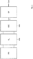
- the passive infrared detector (PIR) is connected with its two connecting lines to an unloading network R G. This in turn is connected to an analog-to-digital converter (ADC).
- ADC analog-to-digital converter
- the output of the analog-to-digital converter is connected via a first bus (T) with a first bus width to a digital filter (DF), the output Out of which typically has a larger second bus width than the first bus width.
- T first bus
- DF digital filter
- the discharge can take place through a leakage resistance between the connections of the sensor or from the connections according to reference ground (R dis_1 , R dis_2 ).
- R dis_1 , R dis_2 reference ground
- a major disadvantage of this solution is the continuous attenuation of the signal and the intrinsic noise of the detector.
- a giga-ohm resistor in low-cost CMOS technology cannot be implemented with reasonable effort. It was recognized that the discharge of the second output via the internal resistance of the current source of the PIR sensor (PIR) did not lead to satisfactory results. It has been shown that the resistance value of these bleeder resistances should be greater than 1MOhm, preferably greater than 10 MOhm, preferably greater than 100 MOhm, and preferably greater than 1 GOhm or preferably greater than 10 GOhm.
- the optimal value of the leakage resistance depends on the respective PIR detector and the respective application and should be adapted from case to case become. In the case of large charge shifts due to rapid temperature changes (temperature shock), disproportionately low leakage resistance values would be necessary, which would almost completely eliminate the signal to be detected.
- the discharge resistances of the discharge network should preferably be made the same and as symmetrical as possible, in the technical language "matching".
- These bleeder resistors can also be more complex circuits that only perform the function of a bleeder resistor, among other things. It was recognized as advantageous to design the bleeder resistances at least partially as a switched capacitor circuit. With such circuits, the relatively high-impedance leakage resistances that may be required can be carried out relatively simply. For the operation of such a switched capacitor network, it is particularly advantageous if it is operated with a non-overlapping two-phase cycle. Of course, single-phase and multi-phase clocks can also be used, but these are generally more complex to implement.
- the requirement for reliable discharge of the PIR detector stands in contrast to the highest possible input resistance of the evaluation circuit. It was therefore recognized that it makes sense to make the Es mean equivalent resistance of at least the discharge resistances of the passive infrared detector dependent on whether a measurement of the infrared radiation potential by means of the passive infrared sensor (PIR detector) is being carried out or not.
- the discharge resistors are switched to a very high-resistance state (measurement state). After the end of the measurement, the discharge resistors are switched to a state that is lower-resistance than the measurement state.
- the state of charge (voltage at the detector) can be measured and the size of the discharge resistors readjusted depending on the state of charge.
- the resistance values are always based on average values over several cycles of the operating cycle of the respective switched capacitor network, provided that one is used for the realization of the discharge resistors. It is therefore an essential idea that the discharge resistances of the PIR detector assume different values depending on the states of the sensor system, at least the states measurement and no measurement / discharge should be realized.
- a ⁇ converter that can be used, for example, consists of a differential amplifier, the current source of which is not symmetrically divided into two branches with symmetrical activation of the transistors of the differential amplifier, as is usual with normal differential amplifiers, but instead of the one normally present common account point for the transistors in the branches of the differential amplifier and the operating current source has a current divider, which divides the current differently depending on an external control value. It can be assumed that the operating current source has a finite internal resistance. In this respect, the use of a real voltage source is also possible.
- This current divider can be realized by a resistor chain which is connected at one end to a transistor of the differential amplifier and at the other end to the other transistor of the differential amplifier.
- a multiplexer now connects the operating current source depending on the external control value with a node of this resistance chain. The current divider thus behaves like a digitally controlled potentiometer, the tap of which is set by the external parameter.
- the current is divided in such a way that the gate-source voltages of the transistors are set by the voltage drop across the resistors of the current divider in such a way that the total current through the two branches corresponds to the current of the operating current source.
- the other connections of the transistors are each connected to a load resistor. It has turned out to be particularly advantageous if these load resistors are designed as real current sources, since then the differential load resistance and thus the differential amplification are particularly large.
- Capacitors that integrate the output signal can be connected in parallel with these load resistors.
- Miller capacities is also conceivable.
- these capacitances carry out the summing ⁇ function of the ⁇ converter and thus eliminate the quantization error by means of a downstream comparator.
- each of the outputs of said passive infrared detector is connected to the control input of an associated input transistor of the differential amplifier described.
- a contact of each of these input transistors is connected to an associated current divider output of a controllable current divider.
- Said current divider distributes the current of a reference current source (I ref ) as a function of a control input to the current divider outputs.
- the other contacts of the transistors are each connected to a load resistor, preferably an integrating filter or a capacitor (C 1 , C 2 ).
- the output values of these integrating filters, ie the working resistances and the capacitances are now compared with one another by at least one comparator.
- the comparator output signal of this comparator is connected to a digital integrating filter which, in addition to said capacities, carries out a second integration.
- the control input of said current divider which divides the current from an operating current source, is connected to the output of the digital integrating filter. If the current divider is controlled in an analog manner, a digital-to-analog converter (DAC) and / or a signal format converter is required which converts the output signal of the digital integrating filter into a suitable format. In the example described here, however, this is not necessary since the multiplexer can be controlled digitally.
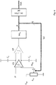
- an output of the passive infrared detector controls at least one second current source.
- This second power source feeds electricity into a first account (S b ).
- This first node (S b ) is connected via an integrating filter to the input of a comparator which compares the signal level of this first node (S b ) with an internal level.
- the output of this comparator is again directly or indirectly connected to said digital integrating filter and thus controls it.
- the output of this digital integrating filter controls a digital-to-analog converter (DAC).
- DAC digital-to-analog converter
- the output of this digital-to-analog converter controls a first current source (I 1 ), which in turn also feeds its current into the first node (S b ).
- one connection of the passive infrared detector is connected to ground, while the other connection is connected to the evaluation circuit described above.
- Such a circuit is also suitable for the evaluation of thermopiles.
- the digital integrating filter is implemented as an up / down counter, which counts in measuring phases in a predetermined or programmable cycle.
- the counting direction is preferably determined by the output of the comparator.
- the step size of this count and the time intervals in which a count is carried out can also be constant and predetermined or programmable. In some applications it has proven useful to make the increment of the count dependent on the meter reading itself in order to avoid an overflow or underflow and thus a total inoperability.
- the counter reading exceeds a critical upper value, this can be detected, for example, and cause the measurement state to be left and the discharge state of the detector element to be activated. This is particularly useful for the single-phase variant, since it is able to measure the absolute level of an input signal.
- the output of the digital integrating filter represents the measured value.
- the quantization error becomes zero in the interference spectrum at a frequency of 0 Hz and tends towards a finite value for infinitely high frequencies.
- the cut-off frequencies depend essentially on the said Load capacities (C 1 , C 2 ) and the resistance (R M ) of the current divider and can be adjusted well.
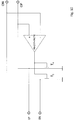
- the discharge current through this circuit depends on the input voltage between the electrical connections IP and IN. In the area A of the input voltage specified by the dimensions, the discharge current disappears except for the leakage current of the transistors. The discharge current increases with increasing distance between the input voltage outside this area A.
- the input resistance RIN (IP-IN) depends on the differential voltage V (IP-IN) between the inputs IP and IN of the network R G.
- the input resistance considered here can be assumed to be located between the connections IP and IN as well as between a connection IP or IN on the one hand and the reference potential, for example ground, on the other.
- the resistance behavior should preferably be similar to that in each of these two considerations Figure 12 be.
- a Voltage range in which the discharge network has a high resistance ADC Analog to digital converter
- B Voltage range in which the discharge network has a medium conductivity C. Voltage range in which the discharge network has a higher conductivity
- C 1 First capacity C 1b First integrating filter (third capacity)
- Another power source I 2 Power source I a1 First current divider output I a2 Second current divider output IN First connection for the PIR sensor Int Integrating filter (in the simplest case an up / down counter) Int b Integrating filter (in the simplest case an up / down counter) IN Second connection for the PIR sensor IN FB Tapping on a resistor cascade (R FB ) from individual resistors
- ON First output of the differential stage OP Second output of the differential stage Out Output bus of the digital filter DF ( downstream filter DF) ⁇ 1 First cycle of the SC network to form a discharge resistor ⁇ 2 Second cycle of the SC network to form a discharge resistor.
- the clock is essentially inverse to ⁇ 1 and does not overlap with ⁇ 1 .
- R dis_2 Second unfavorable discharge resistance in the prior art This leads to a load on the output IN and one Reduction of the output signal. This resistance is modulated in the device.
- the implementation is similar to the implementation of the current divider consisting of multiplexer MUX and resistor cascade R M1 to R Mn .
- R G Unloading network This discharge network prevents the PIR sensor from being charged against both the ground and the connections of the PIR sensor against one another.
- R L1 First working resistance R L2 Second working resistance
- R M1 to R Mn Resistors in the resistor chain made up of n resistors in the current section of the differential stage
- R PIR_C Series resistance of the parasitic capacitance C PIR .
Landscapes
- Engineering & Computer Science (AREA)
- General Physics & Mathematics (AREA)
- Physics & Mathematics (AREA)
- Chemical & Material Sciences (AREA)
- Organic Chemistry (AREA)
- Spectroscopy & Molecular Physics (AREA)
- Life Sciences & Earth Sciences (AREA)
- Health & Medical Sciences (AREA)
- Biochemistry (AREA)
- Food Science & Technology (AREA)
- General Health & Medical Sciences (AREA)
- Wood Science & Technology (AREA)
- Zoology (AREA)
- Genetics & Genomics (AREA)
- Bioinformatics & Cheminformatics (AREA)
- General Engineering & Computer Science (AREA)
- Power Engineering (AREA)
- Theoretical Computer Science (AREA)
- Polymers & Plastics (AREA)
- Nutrition Science (AREA)
- Biotechnology (AREA)
- Photometry And Measurement Of Optical Pulse Characteristics (AREA)
- Geophysics And Detection Of Objects (AREA)
Claims (6)
- Procédé destiné au fonctionnement d'un détecteur infrarouge passif (PIR) réalisé comme dipôle, dans lequel le procédé comprend les étapes :- commande d'une source de courant (I2) par le biais d'une sortie (IP, IN) du détecteur infrarouge passif (PIR),- dans lequel la source de courant (I2) injecte du courant dans un premier nœud (Sb),- dans lequel ce nœud (Sb) est relié par le biais d'un filtre intégrateur (C1b) à l'entrée d'un comparateur (CPb), lequel compare la tension au nœud (Sb) à une valeur de référence,- dans lequel le signal de sortie de ce comparateur (CPb) commande un filtre intégrateur numérique (Intb),- dans lequel le signal de sortie de ce filtre intégrateur numérique (Intb) est conduit à un convertisseur numérique-analogique (DAC),- dans lequel le signal de sortie de ce convertisseur numérique-analogique (DAC) est conduit à une autre source de courant (I1) commandée par le signal de sortie du convertisseur numérique-analogique (DAC) et- dans lequel cette autre source de courant (I1) injecte également son courant dans le premier nœud (Sb).
- Procédé d'après la revendication 1, caractérisé en ce que- le filtre intégrateur numérique est un compteur/décompteur (Intb),- le signal de sortie de comparateur du comparateur (CP) commande au moins ce compteur/décompteur (Intb) dans son sens de comptage et- le compteur/décompteur (Intb) incrémente ou décrémente sa valeur numérique à des intervalles de temps prédéfinis et/ou programmables.
- Procédé selon la revendication 1 ou 2, caractérisé en ce qu'un autre filtre numérique (DF) est ordonné au filtre intégrateur numérique.
- Configuration de circuit destinée au fonctionnement d'un détecteur infrarouge passif (PIR) réalisé comme dipôle, comportant- une première source de courant commandée (I2), un filtre intégrateur (C1b), un comparateur (CPb), un filtre intégrateur numérique (Intb), un convertisseur numérique-analogique (DAC) et une autre source de courant commandée (I1),- dans laquelle la première source de courant (I2) est commandée depuis une sortie (IP, IN) du détecteur infrarouge passif (PIR) et injecte du courant dans un premier nœud (Sb),- dans laquelle ce nœud (Sb) est relié par le biais du filtre intégrateur (C1b) à l'entrée du comparateur (CPb), lequel compare la tension au nœud (Sb) à une valeur de référence,- dans laquelle le signal de sortie de ce comparateur (CPb) commande le filtre intégrateur numérique (Intb),- dans laquelle le signal de sortie de ce filtre intégrateur numérique (Intb) est conduit au convertisseur numérique-analogique (DAC),- dans laquelle le signal de sortie de ce convertisseur numérique-analogique (DAC) est conduit à l'autre source de courant (I1) commandée par le signal de sortie du convertisseur numérique-analogique (DAC) et- dans laquelle cette autre source de courant (I1) injecte également son courant dans le premier nœud (Sb).
- Configuration de circuit selon la revendication 4, caractérisée en ce que- le filtre intégrateur numérique est un compteur/décompteur (Intb),- le signal de sortie de comparateur du comparateur (CPb) commande au moins ce compteur/décompteur (Intb) dans son sens de comptage et- le compteur/décompteur (Intb) incrémente ou décrémente sa valeur numérique à des intervalles de temps prédéfinis et/ou programmables.
- Configuration de circuit selon la revendication 4 ou 5, caractérisée en ce qu'un autre filtre numérique (DF) est disposé en aval du filtre intégrateur numérique.
Applications Claiming Priority (3)
| Application Number | Priority Date | Filing Date | Title |
|---|---|---|---|
| DE102013014810.3A DE102013014810B4 (de) | 2013-09-05 | 2013-09-05 | Vorrichtung zum Betreiben passiver Infrarotsensoren |
| EP13821054.7A EP3042167B1 (fr) | 2013-09-05 | 2013-10-21 | Procédé pour le fonctionnement d'un détecteur infrarouge |
| PCT/DE2013/000624 WO2015032373A2 (fr) | 2013-09-05 | 2013-10-21 | Dispositif de fonctionnement de capteurs infrarouges passifs |
Related Parent Applications (2)
| Application Number | Title | Priority Date | Filing Date |
|---|---|---|---|
| EP13821054.7A Division EP3042167B1 (fr) | 2013-09-05 | 2013-10-21 | Procédé pour le fonctionnement d'un détecteur infrarouge |
| EP13821054.7A Division-Into EP3042167B1 (fr) | 2013-09-05 | 2013-10-21 | Procédé pour le fonctionnement d'un détecteur infrarouge |
Publications (3)
| Publication Number | Publication Date |
|---|---|
| EP3141878A2 EP3141878A2 (fr) | 2017-03-15 |
| EP3141878A3 EP3141878A3 (fr) | 2017-06-07 |
| EP3141878B1 true EP3141878B1 (fr) | 2020-07-15 |
Family
ID=49955791
Family Applications (4)
| Application Number | Title | Priority Date | Filing Date |
|---|---|---|---|
| EP16192823.9A Active EP3141878B1 (fr) | 2013-09-05 | 2013-10-21 | Dispositif et procédé de fonctionnement de capteurs à infrarouge passif |
| EP16192805.6A Withdrawn EP3141877A3 (fr) | 2013-09-05 | 2013-10-21 | Dispositif et procédé de fonctionnement de capteurs à infrarouge passif |
| EP13821054.7A Active EP3042167B1 (fr) | 2013-09-05 | 2013-10-21 | Procédé pour le fonctionnement d'un détecteur infrarouge |
| EP18164330.5A Withdrawn EP3364160A1 (fr) | 2013-09-05 | 2013-10-21 | Dispositif de fonctionnement de capteurs à infrarouge passif |
Family Applications After (3)
| Application Number | Title | Priority Date | Filing Date |
|---|---|---|---|
| EP16192805.6A Withdrawn EP3141877A3 (fr) | 2013-09-05 | 2013-10-21 | Dispositif et procédé de fonctionnement de capteurs à infrarouge passif |
| EP13821054.7A Active EP3042167B1 (fr) | 2013-09-05 | 2013-10-21 | Procédé pour le fonctionnement d'un détecteur infrarouge |
| EP18164330.5A Withdrawn EP3364160A1 (fr) | 2013-09-05 | 2013-10-21 | Dispositif de fonctionnement de capteurs à infrarouge passif |
Country Status (6)
| Country | Link |
|---|---|
| US (2) | US9829382B2 (fr) |
| EP (4) | EP3141878B1 (fr) |
| CN (1) | CN204856807U (fr) |
| DE (1) | DE102013014810B4 (fr) |
| HK (1) | HK1252694A1 (fr) |
| WO (1) | WO2015032373A2 (fr) |
Families Citing this family (5)
| Publication number | Priority date | Publication date | Assignee | Title |
|---|---|---|---|---|
| WO2020030584A1 (fr) * | 2018-08-07 | 2020-02-13 | Signify Holding B.V. | Systèmes et procédés de compression de données de capteur au moyen d'un groupement et d'un appariement de formes dans des nœuds de périphérie de réseaux informatiques répartis |
| NL2024414B1 (en) | 2019-12-10 | 2021-09-01 | Insiava Pty Ltd | An amplifier circuit to enable accurate measurement of small electrical signals |
| JP7758460B2 (ja) * | 2020-02-28 | 2025-10-22 | 浜松ホトニクス株式会社 | 光検出装置 |
| CN111786675B (zh) * | 2020-07-22 | 2022-03-29 | 电子科技大学 | 一种基于动态追踪的电荷共享式模数转换器量化方法 |
| CN113726320B (zh) * | 2021-08-20 | 2023-10-24 | 成都振芯科技股份有限公司 | 一种宽带低功耗高线性数模开关及控制系统与方法 |
Family Cites Families (18)
| Publication number | Priority date | Publication date | Assignee | Title |
|---|---|---|---|---|
| US4377808A (en) * | 1980-07-28 | 1983-03-22 | Sound Engineering (Far East) Limited | Infrared intrusion alarm system |
| JPS62282230A (ja) * | 1986-05-30 | 1987-12-08 | Sumitomo Metal Mining Co Ltd | 焦電型赤外線検知器 |
| CH689071A5 (de) | 1994-03-24 | 1998-08-31 | Cerberus Ag | Signalauswertungsschaltung fuer einen Bewegungsmelder. |
| JP4548562B2 (ja) * | 2001-03-26 | 2010-09-22 | ルネサスエレクトロニクス株式会社 | カレントミラー回路及びアナログデジタル変換回路 |
| JP3778809B2 (ja) * | 2001-04-13 | 2006-05-24 | 富士通メディアデバイス株式会社 | 音叉型振動ジャイロ及びその電極トリミング方法 |
| JP4006985B2 (ja) * | 2001-11-27 | 2007-11-14 | 松下電工株式会社 | 焦電型赤外線検出装置 |
| EP1611558B1 (fr) | 2003-04-07 | 2009-03-11 | Microsystems on Silicon (Pty) Ltd. | Dispositif servant a detecter un parametre physique |
| US7230555B2 (en) * | 2005-02-23 | 2007-06-12 | Analogic Corporation | Sigma delta converter with flying capacitor input |
| US20090302859A1 (en) | 2005-11-16 | 2009-12-10 | Microsystems On Silicon (Pty) Ltd. | Method for testing a passive infrared sensor |
| US7242332B1 (en) | 2006-05-04 | 2007-07-10 | Micron Technology, Inc. | Column-parallel sigma-delta analog-to-digital conversion with gain and offset control |
| US9277629B2 (en) * | 2008-09-03 | 2016-03-01 | Lutron Electronics Co., Inc. | Radio-frequency lighting control system with occupancy sensing |
| US9030213B2 (en) | 2009-01-28 | 2015-05-12 | St-Ericsson Sa | Method and system for measuring a time constant of an integrated circuit, and integrated circuit provided with such a system |
| WO2010110249A1 (fr) * | 2009-03-25 | 2010-09-30 | ローム株式会社 | Capteur d'éclairement lumineux, appareil électronique et dispositif à semi-conducteurs utilisant le capteur d'éclairement lumineux |
| US20100259322A1 (en) * | 2009-04-06 | 2010-10-14 | Bridge Semiconductor Corporation | Readout circuit and system including same |
| JP5685717B2 (ja) * | 2010-07-01 | 2015-03-18 | パナソニックIpマネジメント株式会社 | 赤外線検出装置 |
| SG185665A1 (en) * | 2010-07-01 | 2012-12-28 | Panasonic Corp | Object detection device |
| US8653435B2 (en) * | 2010-09-06 | 2014-02-18 | King Abdulaziz City Science And Technology | Time-delay integration imaging method and apparatus using a high-speed in-pixel analog photon counter |
| AT511664B1 (de) | 2012-10-17 | 2016-01-15 | Avl List Gmbh | Digitaler Ladungsverstärker |
-
2013
- 2013-09-05 DE DE102013014810.3A patent/DE102013014810B4/de active Active
- 2013-10-21 EP EP16192823.9A patent/EP3141878B1/fr active Active
- 2013-10-21 EP EP16192805.6A patent/EP3141877A3/fr not_active Withdrawn
- 2013-10-21 EP EP13821054.7A patent/EP3042167B1/fr active Active
- 2013-10-21 WO PCT/DE2013/000624 patent/WO2015032373A2/fr not_active Ceased
- 2013-10-21 US US14/647,906 patent/US9829382B2/en active Active
- 2013-10-21 EP EP18164330.5A patent/EP3364160A1/fr not_active Withdrawn
- 2013-10-21 CN CN201390000870.8U patent/CN204856807U/zh not_active Expired - Lifetime
-
2017
- 2017-09-15 US US15/705,298 patent/US10444077B2/en active Active
-
2018
- 2018-09-18 HK HK18112002.1A patent/HK1252694A1/zh unknown
Non-Patent Citations (1)
| Title |
|---|
| None * |
Also Published As
| Publication number | Publication date |
|---|---|
| US9829382B2 (en) | 2017-11-28 |
| EP3141877A2 (fr) | 2017-03-15 |
| US20150308900A1 (en) | 2015-10-29 |
| WO2015032373A2 (fr) | 2015-03-12 |
| HK1252694A1 (zh) | 2019-05-31 |
| WO2015032373A3 (fr) | 2015-06-18 |
| EP3141877A3 (fr) | 2017-06-07 |
| DE102013014810A1 (de) | 2015-03-05 |
| CN204856807U (zh) | 2015-12-09 |
| HK1220506A1 (zh) | 2017-05-05 |
| EP3141878A3 (fr) | 2017-06-07 |
| DE102013014810B4 (de) | 2019-03-14 |
| US20180017445A1 (en) | 2018-01-18 |
| US10444077B2 (en) | 2019-10-15 |
| EP3364160A1 (fr) | 2018-08-22 |
| EP3042167B1 (fr) | 2018-08-01 |
| EP3141878A2 (fr) | 2017-03-15 |
| EP3042167A2 (fr) | 2016-07-13 |
Similar Documents
| Publication | Publication Date | Title |
|---|---|---|
| DE102014105886B4 (de) | Schaltungsanordnung und Verfahren zur Reproduktion eines Stroms | |
| DE102007042315B3 (de) | Messkreis mit geschalteten Kondensator zur Messung der Kapazität eines Eingangskondensators | |
| EP3141878B1 (fr) | Dispositif et procédé de fonctionnement de capteurs à infrarouge passif | |
| WO2007115710A1 (fr) | Dispositif convertisseur analogique-numérique et procédé correspondant | |
| DE69219749T2 (de) | Zeit-konstante Detektionsschaltung und Zeit-konstante Regelungschaltung | |
| DE102012209717A1 (de) | Analog-Digital-Wandler | |
| DE102013222252B4 (de) | Verfahren und Schaltung für einen Analog-Digital-Kapazitätswandler | |
| DE3017669C2 (de) | Verstärkerschaltungsanordnung | |
| DE112004001469T5 (de) | Geschalteter Ladungs-Multiplizierer-Dividierer | |
| DE102012208299B4 (de) | Auf Zweiphasenschwellendetektoren basierende Schaltungen | |
| DE102009002062B4 (de) | Analog-Digital-Umsetzer mit breitbandigem Eingangsnetzwerk | |
| EP1067473B1 (fr) | Intégrateur | |
| DE102006017239B4 (de) | Differentieller Levelshifter mit automatischem Fehlerabgleich | |
| DE102013022381B3 (de) | Vorrichtung zum Betreiben passiver Infrarotsensoren | |
| DE102013022378B3 (de) | Vorrichtung zum Betreiben passiver Infrarotsensoren | |
| DE202013012209U1 (de) | Vorrichtung zum Betreiben passiver Infrarotsensoren | |
| DE102013022377B3 (de) | Vorrichtung zum Betreiben passiver Infrarotsensoren | |
| DE102013022547B4 (de) | Vorrichtung zum Betreiben passiver Infrarotsensoren | |
| DE202013007940U1 (de) | Vorrrichtung zum Betreiben passiver Infrarotsensoren | |
| DE102013022759B4 (de) | Vorrichtung zum Betreiben passiver lnfrarotsensoren | |
| DE102013022763B4 (de) | Vorrichtung zum Betreiben passiver Infrarotsensoren | |
| DE202013012208U1 (de) | Vorrichtung zum Betreiben passiver Infrarotsensoren | |
| DE202013012213U1 (de) | Vorrichtung zum Betreiben passiver Infrarotsensoren | |
| DE202013012211U1 (de) | Vorrichtung zum Betreiben passiver Infrarotsensoren | |
| DE202013012210U1 (de) | Vorrichtung zum Betreiben passiver Infrarotsensoren |
Legal Events
| Date | Code | Title | Description |
|---|---|---|---|
| PUAI | Public reference made under article 153(3) epc to a published international application that has entered the european phase |
Free format text: ORIGINAL CODE: 0009012 |
|
| STAA | Information on the status of an ep patent application or granted ep patent |
Free format text: STATUS: THE APPLICATION HAS BEEN PUBLISHED |
|
| AC | Divisional application: reference to earlier application |
Ref document number: 3042167 Country of ref document: EP Kind code of ref document: P |
|
| AK | Designated contracting states |
Kind code of ref document: A2 Designated state(s): AL AT BE BG CH CY CZ DE DK EE ES FI FR GB GR HR HU IE IS IT LI LT LU LV MC MK MT NL NO PL PT RO RS SE SI SK SM TR |
|
| AK | Designated contracting states |
Kind code of ref document: A3 Designated state(s): AL AT BE BG CH CY CZ DE DK EE ES FI FR GB GR HR HU IE IS IT LI LT LU LV MC MK MT NL NO PL PT RO RS SE SI SK SM TR |
|
| RIC1 | Information provided on ipc code assigned before grant |
Ipc: H03F 3/70 20060101ALI20170428BHEP Ipc: H03F 3/45 20060101ALI20170428BHEP Ipc: G01J 1/46 20060101AFI20170428BHEP Ipc: H03M 3/00 20060101ALI20170428BHEP Ipc: G08B 13/191 20060101ALI20170428BHEP Ipc: G01J 5/10 20060101ALI20170428BHEP |
|
| PUAL | Search report despatched |
Free format text: ORIGINAL CODE: 0009013 |
|
| STAA | Information on the status of an ep patent application or granted ep patent |
Free format text: STATUS: REQUEST FOR EXAMINATION WAS MADE |
|
| 17P | Request for examination filed |
Effective date: 20171206 |
|
| RBV | Designated contracting states (corrected) |
Designated state(s): AL AT BE BG CH CY CZ DE DK EE ES FI FR GB GR HR HU IE IS IT LI LT LU LV MC MK MT NL NO PL PT RO RS SE SI SK SM TR |
|
| RIN1 | Information on inventor provided before grant (corrected) |
Inventor name: SUNTKEN, ARTUR |
|
| STAA | Information on the status of an ep patent application or granted ep patent |
Free format text: STATUS: EXAMINATION IS IN PROGRESS |
|
| 17Q | First examination report despatched |
Effective date: 20180419 |
|
| GRAP | Despatch of communication of intention to grant a patent |
Free format text: ORIGINAL CODE: EPIDOSNIGR1 |
|
| STAA | Information on the status of an ep patent application or granted ep patent |
Free format text: STATUS: GRANT OF PATENT IS INTENDED |
|
| INTG | Intention to grant announced |
Effective date: 20200207 |
|
| GRAS | Grant fee paid |
Free format text: ORIGINAL CODE: EPIDOSNIGR3 |
|
| GRAA | (expected) grant |
Free format text: ORIGINAL CODE: 0009210 |
|
| STAA | Information on the status of an ep patent application or granted ep patent |
Free format text: STATUS: THE PATENT HAS BEEN GRANTED |
|
| AC | Divisional application: reference to earlier application |
Ref document number: 3042167 Country of ref document: EP Kind code of ref document: P |
|
| AK | Designated contracting states |
Kind code of ref document: B1 Designated state(s): AL AT BE BG CH CY CZ DE DK EE ES FI FR GB GR HR HU IE IS IT LI LT LU LV MC MK MT NL NO PL PT RO RS SE SI SK SM TR |
|
| REG | Reference to a national code |
Ref country code: CH Ref legal event code: EP Ref country code: GB Ref legal event code: FG4D Free format text: NOT ENGLISH |
|
| REG | Reference to a national code |
Ref country code: IE Ref legal event code: FG4D Free format text: LANGUAGE OF EP DOCUMENT: GERMAN |
|
| REG | Reference to a national code |
Ref country code: DE Ref legal event code: R096 Ref document number: 502013014931 Country of ref document: DE |
|
| REG | Reference to a national code |
Ref country code: DE Ref legal event code: R081 Ref document number: 502013014931 Country of ref document: DE Owner name: ELMOS SEMICONDUCTOR SE, DE Free format text: FORMER OWNER: ELMOS SEMICONDUCTOR AKTIENGESELLSCHAFT, 44227 DORTMUND, DE |
|
| REG | Reference to a national code |
Ref country code: AT Ref legal event code: REF Ref document number: 1291532 Country of ref document: AT Kind code of ref document: T Effective date: 20200815 |
|
| RAP2 | Party data changed (patent owner data changed or rights of a patent transferred) |
Owner name: ELMOS SEMICONDUCTOR SE |
|
| REG | Reference to a national code |
Ref country code: LT Ref legal event code: MG4D |
|
| REG | Reference to a national code |
Ref country code: NL Ref legal event code: MP Effective date: 20200715 |
|
| PG25 | Lapsed in a contracting state [announced via postgrant information from national office to epo] |
Ref country code: PT Free format text: LAPSE BECAUSE OF FAILURE TO SUBMIT A TRANSLATION OF THE DESCRIPTION OR TO PAY THE FEE WITHIN THE PRESCRIBED TIME-LIMIT Effective date: 20201116 Ref country code: BG Free format text: LAPSE BECAUSE OF FAILURE TO SUBMIT A TRANSLATION OF THE DESCRIPTION OR TO PAY THE FEE WITHIN THE PRESCRIBED TIME-LIMIT Effective date: 20201015 Ref country code: SE Free format text: LAPSE BECAUSE OF FAILURE TO SUBMIT A TRANSLATION OF THE DESCRIPTION OR TO PAY THE FEE WITHIN THE PRESCRIBED TIME-LIMIT Effective date: 20200715 Ref country code: NO Free format text: LAPSE BECAUSE OF FAILURE TO SUBMIT A TRANSLATION OF THE DESCRIPTION OR TO PAY THE FEE WITHIN THE PRESCRIBED TIME-LIMIT Effective date: 20201015 Ref country code: HR Free format text: LAPSE BECAUSE OF FAILURE TO SUBMIT A TRANSLATION OF THE DESCRIPTION OR TO PAY THE FEE WITHIN THE PRESCRIBED TIME-LIMIT Effective date: 20200715 Ref country code: LT Free format text: LAPSE BECAUSE OF FAILURE TO SUBMIT A TRANSLATION OF THE DESCRIPTION OR TO PAY THE FEE WITHIN THE PRESCRIBED TIME-LIMIT Effective date: 20200715 Ref country code: ES Free format text: LAPSE BECAUSE OF FAILURE TO SUBMIT A TRANSLATION OF THE DESCRIPTION OR TO PAY THE FEE WITHIN THE PRESCRIBED TIME-LIMIT Effective date: 20200715 Ref country code: GR Free format text: LAPSE BECAUSE OF FAILURE TO SUBMIT A TRANSLATION OF THE DESCRIPTION OR TO PAY THE FEE WITHIN THE PRESCRIBED TIME-LIMIT Effective date: 20201016 Ref country code: FI Free format text: LAPSE BECAUSE OF FAILURE TO SUBMIT A TRANSLATION OF THE DESCRIPTION OR TO PAY THE FEE WITHIN THE PRESCRIBED TIME-LIMIT Effective date: 20200715 |
|
| PG25 | Lapsed in a contracting state [announced via postgrant information from national office to epo] |
Ref country code: LV Free format text: LAPSE BECAUSE OF FAILURE TO SUBMIT A TRANSLATION OF THE DESCRIPTION OR TO PAY THE FEE WITHIN THE PRESCRIBED TIME-LIMIT Effective date: 20200715 Ref country code: RS Free format text: LAPSE BECAUSE OF FAILURE TO SUBMIT A TRANSLATION OF THE DESCRIPTION OR TO PAY THE FEE WITHIN THE PRESCRIBED TIME-LIMIT Effective date: 20200715 Ref country code: PL Free format text: LAPSE BECAUSE OF FAILURE TO SUBMIT A TRANSLATION OF THE DESCRIPTION OR TO PAY THE FEE WITHIN THE PRESCRIBED TIME-LIMIT Effective date: 20200715 Ref country code: IS Free format text: LAPSE BECAUSE OF FAILURE TO SUBMIT A TRANSLATION OF THE DESCRIPTION OR TO PAY THE FEE WITHIN THE PRESCRIBED TIME-LIMIT Effective date: 20201115 |
|
| PG25 | Lapsed in a contracting state [announced via postgrant information from national office to epo] |
Ref country code: NL Free format text: LAPSE BECAUSE OF FAILURE TO SUBMIT A TRANSLATION OF THE DESCRIPTION OR TO PAY THE FEE WITHIN THE PRESCRIBED TIME-LIMIT Effective date: 20200715 |
|
| REG | Reference to a national code |
Ref country code: DE Ref legal event code: R097 Ref document number: 502013014931 Country of ref document: DE |
|
| PG25 | Lapsed in a contracting state [announced via postgrant information from national office to epo] |
Ref country code: EE Free format text: LAPSE BECAUSE OF FAILURE TO SUBMIT A TRANSLATION OF THE DESCRIPTION OR TO PAY THE FEE WITHIN THE PRESCRIBED TIME-LIMIT Effective date: 20200715 Ref country code: IT Free format text: LAPSE BECAUSE OF FAILURE TO SUBMIT A TRANSLATION OF THE DESCRIPTION OR TO PAY THE FEE WITHIN THE PRESCRIBED TIME-LIMIT Effective date: 20200715 Ref country code: SM Free format text: LAPSE BECAUSE OF FAILURE TO SUBMIT A TRANSLATION OF THE DESCRIPTION OR TO PAY THE FEE WITHIN THE PRESCRIBED TIME-LIMIT Effective date: 20200715 Ref country code: RO Free format text: LAPSE BECAUSE OF FAILURE TO SUBMIT A TRANSLATION OF THE DESCRIPTION OR TO PAY THE FEE WITHIN THE PRESCRIBED TIME-LIMIT Effective date: 20200715 Ref country code: DK Free format text: LAPSE BECAUSE OF FAILURE TO SUBMIT A TRANSLATION OF THE DESCRIPTION OR TO PAY THE FEE WITHIN THE PRESCRIBED TIME-LIMIT Effective date: 20200715 Ref country code: CZ Free format text: LAPSE BECAUSE OF FAILURE TO SUBMIT A TRANSLATION OF THE DESCRIPTION OR TO PAY THE FEE WITHIN THE PRESCRIBED TIME-LIMIT Effective date: 20200715 |
|
| PLBE | No opposition filed within time limit |
Free format text: ORIGINAL CODE: 0009261 |
|
| STAA | Information on the status of an ep patent application or granted ep patent |
Free format text: STATUS: NO OPPOSITION FILED WITHIN TIME LIMIT |
|
| PG25 | Lapsed in a contracting state [announced via postgrant information from national office to epo] |
Ref country code: AL Free format text: LAPSE BECAUSE OF FAILURE TO SUBMIT A TRANSLATION OF THE DESCRIPTION OR TO PAY THE FEE WITHIN THE PRESCRIBED TIME-LIMIT Effective date: 20200715 |
|
| REG | Reference to a national code |
Ref country code: CH Ref legal event code: PL |
|
| 26N | No opposition filed |
Effective date: 20210416 |
|
| GBPC | Gb: european patent ceased through non-payment of renewal fee |
Effective date: 20201021 |
|
| PG25 | Lapsed in a contracting state [announced via postgrant information from national office to epo] |
Ref country code: MC Free format text: LAPSE BECAUSE OF FAILURE TO SUBMIT A TRANSLATION OF THE DESCRIPTION OR TO PAY THE FEE WITHIN THE PRESCRIBED TIME-LIMIT Effective date: 20200715 Ref country code: LU Free format text: LAPSE BECAUSE OF NON-PAYMENT OF DUE FEES Effective date: 20201021 Ref country code: SK Free format text: LAPSE BECAUSE OF FAILURE TO SUBMIT A TRANSLATION OF THE DESCRIPTION OR TO PAY THE FEE WITHIN THE PRESCRIBED TIME-LIMIT Effective date: 20200715 |
|
| REG | Reference to a national code |
Ref country code: BE Ref legal event code: MM Effective date: 20201031 |
|
| PG25 | Lapsed in a contracting state [announced via postgrant information from national office to epo] |
Ref country code: CH Free format text: LAPSE BECAUSE OF NON-PAYMENT OF DUE FEES Effective date: 20201031 Ref country code: BE Free format text: LAPSE BECAUSE OF NON-PAYMENT OF DUE FEES Effective date: 20201031 Ref country code: SI Free format text: LAPSE BECAUSE OF FAILURE TO SUBMIT A TRANSLATION OF THE DESCRIPTION OR TO PAY THE FEE WITHIN THE PRESCRIBED TIME-LIMIT Effective date: 20200715 Ref country code: LI Free format text: LAPSE BECAUSE OF NON-PAYMENT OF DUE FEES Effective date: 20201031 Ref country code: GB Free format text: LAPSE BECAUSE OF NON-PAYMENT OF DUE FEES Effective date: 20201021 |
|
| PG25 | Lapsed in a contracting state [announced via postgrant information from national office to epo] |
Ref country code: IE Free format text: LAPSE BECAUSE OF NON-PAYMENT OF DUE FEES Effective date: 20201021 |
|
| REG | Reference to a national code |
Ref country code: AT Ref legal event code: MM01 Ref document number: 1291532 Country of ref document: AT Kind code of ref document: T Effective date: 20201021 |
|
| PG25 | Lapsed in a contracting state [announced via postgrant information from national office to epo] |
Ref country code: AT Free format text: LAPSE BECAUSE OF NON-PAYMENT OF DUE FEES Effective date: 20201021 |
|
| PG25 | Lapsed in a contracting state [announced via postgrant information from national office to epo] |
Ref country code: TR Free format text: LAPSE BECAUSE OF FAILURE TO SUBMIT A TRANSLATION OF THE DESCRIPTION OR TO PAY THE FEE WITHIN THE PRESCRIBED TIME-LIMIT Effective date: 20200715 Ref country code: MT Free format text: LAPSE BECAUSE OF FAILURE TO SUBMIT A TRANSLATION OF THE DESCRIPTION OR TO PAY THE FEE WITHIN THE PRESCRIBED TIME-LIMIT Effective date: 20200715 Ref country code: CY Free format text: LAPSE BECAUSE OF FAILURE TO SUBMIT A TRANSLATION OF THE DESCRIPTION OR TO PAY THE FEE WITHIN THE PRESCRIBED TIME-LIMIT Effective date: 20200715 |
|
| PG25 | Lapsed in a contracting state [announced via postgrant information from national office to epo] |
Ref country code: MK Free format text: LAPSE BECAUSE OF FAILURE TO SUBMIT A TRANSLATION OF THE DESCRIPTION OR TO PAY THE FEE WITHIN THE PRESCRIBED TIME-LIMIT Effective date: 20200715 |
|
| P01 | Opt-out of the competence of the unified patent court (upc) registered |
Effective date: 20230525 |
|
| REG | Reference to a national code |
Ref country code: DE Ref legal event code: R081 Ref document number: 502013014931 Country of ref document: DE Owner name: ELMOS SEMICONDUCTOR SE, DE Free format text: FORMER OWNER: ELMOS SEMICONDUCTOR SE, 44227 DORTMUND, DE |
|
| PGFP | Annual fee paid to national office [announced via postgrant information from national office to epo] |
Ref country code: DE Payment date: 20251015 Year of fee payment: 13 |
|
| PGFP | Annual fee paid to national office [announced via postgrant information from national office to epo] |
Ref country code: FR Payment date: 20251029 Year of fee payment: 13 |