EP3141961A2 - Unite d'eclairage et dispositif d'eclairage lithographique - Google Patents
Unite d'eclairage et dispositif d'eclairage lithographique Download PDFInfo
- Publication number
- EP3141961A2 EP3141961A2 EP16184526.8A EP16184526A EP3141961A2 EP 3141961 A2 EP3141961 A2 EP 3141961A2 EP 16184526 A EP16184526 A EP 16184526A EP 3141961 A2 EP3141961 A2 EP 3141961A2
- Authority
- EP
- European Patent Office
- Prior art keywords
- lighting unit
- illumination
- photomask
- homogenizing element
- source
- Prior art date
- Legal status (The legal status is an assumption and is not a legal conclusion. Google has not performed a legal analysis and makes no representation as to the accuracy of the status listed.)
- Granted
Links
Images
Classifications
-
- G—PHYSICS
- G03—PHOTOGRAPHY; CINEMATOGRAPHY; ANALOGOUS TECHNIQUES USING WAVES OTHER THAN OPTICAL WAVES; ELECTROGRAPHY; HOLOGRAPHY
- G03F—PHOTOMECHANICAL PRODUCTION OF TEXTURED OR PATTERNED SURFACES, e.g. FOR PRINTING, FOR PROCESSING OF SEMICONDUCTOR DEVICES; MATERIALS THEREFOR; ORIGINALS THEREFOR; APPARATUS SPECIALLY ADAPTED THEREFOR
- G03F7/00—Photomechanical, e.g. photolithographic, production of textured or patterned surfaces, e.g. printing surfaces; Materials therefor, e.g. comprising photoresists; Apparatus specially adapted therefor
- G03F7/70—Microphotolithographic exposure; Apparatus therefor
- G03F7/70058—Mask illumination systems
- G03F7/70075—Homogenization of illumination intensity in the mask plane by using an integrator, e.g. fly's eye lens, facet mirror or glass rod, by using a diffusing optical element or by beam deflection
-
- G—PHYSICS
- G02—OPTICS
- G02B—OPTICAL ELEMENTS, SYSTEMS OR APPARATUS
- G02B26/00—Optical devices or arrangements for the control of light using movable or deformable optical elements
- G02B26/08—Optical devices or arrangements for the control of light using movable or deformable optical elements for controlling the direction of light
- G02B26/0816—Optical devices or arrangements for the control of light using movable or deformable optical elements for controlling the direction of light by means of one or more reflecting elements
- G02B26/0833—Optical devices or arrangements for the control of light using movable or deformable optical elements for controlling the direction of light by means of one or more reflecting elements the reflecting element being a micromechanical device, e.g. a MEMS mirror, DMD
-
- G—PHYSICS
- G02—OPTICS
- G02B—OPTICAL ELEMENTS, SYSTEMS OR APPARATUS
- G02B26/00—Optical devices or arrangements for the control of light using movable or deformable optical elements
- G02B26/08—Optical devices or arrangements for the control of light using movable or deformable optical elements for controlling the direction of light
- G02B26/10—Scanning systems
- G02B26/101—Scanning systems with both horizontal and vertical deflecting means, e.g. raster or XY scanners
-
- G—PHYSICS
- G02—OPTICS
- G02B—OPTICAL ELEMENTS, SYSTEMS OR APPARATUS
- G02B26/00—Optical devices or arrangements for the control of light using movable or deformable optical elements
- G02B26/08—Optical devices or arrangements for the control of light using movable or deformable optical elements for controlling the direction of light
- G02B26/10—Scanning systems
- G02B26/105—Scanning systems with one or more pivoting mirrors or galvano-mirrors
-
- G—PHYSICS
- G02—OPTICS
- G02B—OPTICAL ELEMENTS, SYSTEMS OR APPARATUS
- G02B27/00—Optical systems or apparatus not provided for by any of the groups G02B1/00 - G02B26/00, G02B30/00
- G02B27/09—Beam shaping, e.g. changing the cross-sectional area, not otherwise provided for
- G02B27/0938—Using specific optical elements
- G02B27/0944—Diffractive optical elements, e.g. gratings, holograms
-
- G—PHYSICS
- G02—OPTICS
- G02B—OPTICAL ELEMENTS, SYSTEMS OR APPARATUS
- G02B27/00—Optical systems or apparatus not provided for by any of the groups G02B1/00 - G02B26/00, G02B30/00
- G02B27/09—Beam shaping, e.g. changing the cross-sectional area, not otherwise provided for
- G02B27/0938—Using specific optical elements
- G02B27/095—Refractive optical elements
- G02B27/0955—Lenses
-
- G—PHYSICS
- G02—OPTICS
- G02B—OPTICAL ELEMENTS, SYSTEMS OR APPARATUS
- G02B27/00—Optical systems or apparatus not provided for by any of the groups G02B1/00 - G02B26/00, G02B30/00
- G02B27/42—Diffraction optics, i.e. systems including a diffractive element being designed for providing a diffractive effect
- G02B27/4233—Diffraction optics, i.e. systems including a diffractive element being designed for providing a diffractive effect having a diffractive element [DOE] contributing to a non-imaging application
- G02B27/425—Diffraction optics, i.e. systems including a diffractive element being designed for providing a diffractive effect having a diffractive element [DOE] contributing to a non-imaging application in illumination systems
-
- G—PHYSICS
- G03—PHOTOGRAPHY; CINEMATOGRAPHY; ANALOGOUS TECHNIQUES USING WAVES OTHER THAN OPTICAL WAVES; ELECTROGRAPHY; HOLOGRAPHY
- G03F—PHOTOMECHANICAL PRODUCTION OF TEXTURED OR PATTERNED SURFACES, e.g. FOR PRINTING, FOR PROCESSING OF SEMICONDUCTOR DEVICES; MATERIALS THEREFOR; ORIGINALS THEREFOR; APPARATUS SPECIALLY ADAPTED THEREFOR
- G03F7/00—Photomechanical, e.g. photolithographic, production of textured or patterned surfaces, e.g. printing surfaces; Materials therefor, e.g. comprising photoresists; Apparatus specially adapted therefor
- G03F7/70—Microphotolithographic exposure; Apparatus therefor
- G03F7/70058—Mask illumination systems
- G03F7/7015—Details of optical elements
- G03F7/70158—Diffractive optical elements
-
- G—PHYSICS
- G03—PHOTOGRAPHY; CINEMATOGRAPHY; ANALOGOUS TECHNIQUES USING WAVES OTHER THAN OPTICAL WAVES; ELECTROGRAPHY; HOLOGRAPHY
- G03F—PHOTOMECHANICAL PRODUCTION OF TEXTURED OR PATTERNED SURFACES, e.g. FOR PRINTING, FOR PROCESSING OF SEMICONDUCTOR DEVICES; MATERIALS THEREFOR; ORIGINALS THEREFOR; APPARATUS SPECIALLY ADAPTED THEREFOR
- G03F7/00—Photomechanical, e.g. photolithographic, production of textured or patterned surfaces, e.g. printing surfaces; Materials therefor, e.g. comprising photoresists; Apparatus specially adapted therefor
- G03F7/70—Microphotolithographic exposure; Apparatus therefor
- G03F7/70483—Information management; Active and passive control; Testing; Wafer monitoring, e.g. pattern monitoring
- G03F7/7055—Exposure light control in all parts of the microlithographic apparatus, e.g. pulse length control or light interruption
- G03F7/70583—Speckle reduction, e.g. coherence control or amplitude/wavefront splitting
Definitions
- the invention relates to a lighting unit for lithographic exposure and a device for lithographic exposure with such a lighting unit.
- lithographic methods are often used.
- a radiation-sensitive polymer layer resist
- the introduced radiation dose changes the polymer properties in such a way that in a subsequent development step only the irradiated (positive resist) or only the unirradiated (negative resist) regions of the polymer layer are selectively dissolved and thus removed.
- Lithography systems used in microelectronics and microsystem technology often use a so-called mask aligner, ie a device for the exact positioning of photomasks.
- the light of the shortest possible source of radiation for example a high-pressure mercury lamp
- This photomask contains to be exposed in the radiation-sensitive polymer layer structures in the form of transparent and non-transparent areas, the z. B. are incorporated in a thin chromium layer on a mask substrate. In the transparent areas, the chromium layer is selectively removed.
- the illumination light is correspondingly modulated as it passes through the photomask.
- the polymer layer to be exposed is located on a substrate which is brought into direct contact with the photomask (so-called contact printing) or is located at a small distance of a few micrometers to the photomask (so-called proximity printing).
- a laser can be used with which a significantly higher degree of collimation of the illumination can be achieved.
- the high coherence of lasers in a conventional illumination beam path of the mask aligner results in the occurrence of locally high-frequency interference patterns (so-called speckles), which locally deteriorate the homogeneity of the mask illumination and lead to unusable exposure results.
- An object to be solved is thus to provide a lighting unit and a device for lithographic exposure, which overcomes the aforementioned disadvantages and allows a homogeneous mask lighting with a defined and selectively adjustable illumination angle distribution.
- the illumination unit for lithographic exposure comprises a beam source, the beam source preferably being a laser light source, an electronically controllable beam deflection element suitable for two-dimensional beam deflection, a collimating lens, a beam homogenization element, a Fourier lens and a field lens for telecentric illumination Photomask is provided.
- the specified elements are preferably arranged in the stated sequence in the beam path of the illumination unit. This does not exclude that one or more further elements can be arranged between the mentioned elements.
- a polarizing optical element may be arranged between the beam source and the beam deflection element.
- a defined angular distribution in the directions perpendicular to the optical axis is advantageously generated by means of the two-dimensional beam deflection element, for example in an x-direction and a y-direction, which are orthogonal to one another and each extend perpendicular to the optical axis.
- the light of the beam source is directed onto the collimating lens following the beam deflecting element with a specifically set angular distribution.
- an angular distribution of up to ⁇ 20 ° in the x and y directions can be generated with the beam deflection element.
- the incident radiation is collimated with the defined angular distribution, ie deflected in such a way that it is parallel to the optical axis spreads.
- the collimated radiation subsequently impinges on a beam homogenizing element which generates a defined angular distribution and advantageously homogenizes the radiation.
- the beam homogenizing element acts in particular as a diffuser.
- the beam homogenizing element can in particular homogenize a locally high-frequency interference pattern of the laser light source.
- the beam homogenizing element can produce an angular distribution of about ⁇ 9 ° in the x and y directions.
- a spatial intensity distribution in the plane of the field lens is generated by means of a lens system comprising a Fourier lens and a field lens.
- the field lens has the function of telecentrically illuminating a photomask in a lithographic apparatus.
- the beam deflection element is advantageously an electronically controllable beam deflection element that generates a time-varying beam deflection in two spatial directions.
- the time-varying beam deflection projects the beam of the beam source in this way onto a surface, in particular onto the collimating lens following the beam source.
- the beam deflection element is a scanning beam deflection element that illuminates an area that is large in comparison to the beam diameter of the beam source due to the temporally varying beam deflection.
- the beam deflector for two-dimensional beam deflection is preferably a 2D mirror scanner, i. a mirror scanner that can effect beam deflection in two axes.
- Such mirror scanners are known per se and are used for example in projection devices.
- the mirror scanner may, for example, comprise two mirrors rotatable by a drive, one mirror causing a beam deflection in the x-direction and a second mirror causing a beam deflection in the y-direction, the x-direction and the y-direction being perpendicular to each other and in particular in each case perpendicular to the optical axis.
- the 2D mirror scanner is a galvanometer scanner, or galvo scanner for short.
- the two mirrors are advantageously moved by a galvanic drive.
- a galvanometer scanner is characterized by the fact that the mirrors can be moved at a high speed.
- the mirrors can be moved at a positioning speed of up to 15 m / s.
- another 2D mirror scanner for example a MEMS mirror scanner (micro-electro-mechanical system).
- the beam deflection element has, according to a preferred embodiment, an electronic control unit with which, in particular, the angular distribution of the beam deflection can be set.
- the beam deflection element may have a computer control.
- the control of the beam deflecting element can be integrated, for example, in a computer control of the lighting device and / or the entire lithographic device.
- the beam homogenizing element preferably has a diffractive structure for producing a defined angular distribution of the radiation.
- the beam homogenizing element is a diffractive optical element (DOE) according to at least one embodiment.
- the diffractive optical element may, for example, comprise at least one computer-generated hologram (CGH).
- CGH computer-generated hologram
- the beam homogenizing element can be a refractive-diffractive optical element, that is to say a hybrid element which simultaneously has diffractive properties and refractive interfaces.
- the beam homogenizing element is movable.
- the beam homogenizing element may have an electronic control, which is set up to move the beam homogenizing element during operation of the lighting device.
- the electronic control may be a computer control, which may be integrated in particular in a computer control of the lighting unit and / or the lithographic device.
- the beam homogenizing element may in particular be designed to execute a rotational movement about at least one axis and / or a translational movement in at least one direction during operation of the illumination unit.
- the beam homogenizing element is rotatable about a non-collinear to the optical axis of the illumination device extending axis of rotation, but the axis of rotation is moved parallel to the optical axis and / or tilted.
- the beam homogenizing element eccentrically rotatable.
- the beam homogenizing element By the translational and / or rotational movement of the beam homogenizing element during operation of the lighting unit, it is advantageously achieved that different regions of the beam homogenizing element, in particular the diffractive structure of the beam homogenizing element, are moved into the illuminating beam in a time-varying manner. In this way, it is possible, in particular, to minimize locally high-frequency interference patterns, which can be produced by coherent illumination by means of a laser light source, and thus to homogenize the illumination beam. In this way, a particularly homogeneous angular distribution behind the beam homogenizing element is advantageously achieved, which is transferred by the subsequent lens system of the Fourier lens and the field lens in a homogeneous intensity and angular distribution in the illumination plane of a photomask.
- the beam homogenizing element has a multiplicity of diffractive optical elements, such as holograms, which are preferably arranged next to one another in a 2-dimensional arrangement.
- the movement of the beam homogenizing element can advantageously rotate various diffractive elements through the illumination beam.
- By a continuous movement of the Strahlhomogenticianselements during an exposure process so a homogenization of the illumination light can be achieved. It is also advantageously possible by targeted illumination of certain areas of the beam homogenizing element a desired To produce angular distribution of the illumination light.
- the beam source of the illumination unit is preferably a laser light source.
- a laser light source has the particular advantage that a polarized illumination can take place without loss of light power on a polarizer.
- an excimer laser such as an ArF laser or KrF laser or a solid-state laser such as an Nd: YAG laser can be used as the beam source.
- a laser diode, an LED or a supercontinuum source can be used as the beam source.
- the laser light source can be operated with a frequency conversion, in particular a frequency doubling or frequency tripling. This is particularly advantageous in solid state lasers such as an Nd: YAG laser to provide a comparatively large output wavelength of e.g. 1064 nm into a shorter wavelength of 532 nm or 335 nm.
- the use of short wavelengths is advantageous in lithography for high resolution.
- a polarizing optical element is arranged between the beam source and the beam deflecting element. This is particularly advantageous if the beam source itself is not polarized.
- the polarizing optical element may be, for example, a wire grid polarizer, an A / 2 plate, an A / 4 plate, a Pockels cell or a diffractive optical element.
- a lithographic apparatus having a previously described illumination source and a photomask.
- the beam homogenizing element of Illumination source is advantageously arranged in the Fourier plane of the photomask for generating a homogeneous angular distribution of the illuminating light impinging on the photomask.
- the photomask has a mask structure, which is imaged by means of the generated illumination light into a radiation-sensitive polymer layer (resist).
- the radiation-sensitive polymer layer can be arranged, for example, on a substrate that is positioned in the beam path behind the photomask.
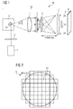
- the illustrated lithographic exposure apparatus 20 includes a lighting unit 10 which is provided to illuminate a photomask 8 with an illuminating light 9.
- the illumination unit 10 comprises a beam source 1, which is preferably a laser light source.
- a beam source 1 which is preferably a laser light source.
- the beam source 1 may have a power of about 1.5 W to 4 W and a beam diameter of about 1 mm.
- polarized illumination light 9 is emitted without loss of light intensity at a polarizer.
- an unpolarized beam source 1 can be used. It is possible that a polarizing optical element 2 is arranged in the beam path, which polarizes the radiation 9 emitted by the beam source 1 or changes the polarization state.
- the polarizing optical element 2 may be, for example, a wire grid polarizer, an A / 2 plate, an A / 4 plate, a Pockels cell or a diffractive optical element.
- the beam source 1 follows in the beam path a beam deflection element 3.
- the beam deflection element 3 is preferably a 2D mirror scanner which contains two movable mirrors which advantageously permit a beam deflection in two mutually perpendicular axes.
- side view is only one of the two Mirror 31 visible, for example, causes a beam deflection in the y direction.
- Another in FIG. 1 invisible mirror causes an additional beam deflection in an x-direction, which is perpendicular to the plane of the drawing.
- the 2D mirror scanner can be, for example, a galvanometer scanner in which the mirrors 31 are galvanically driven.
- the beam deflection element 3 can, for example, allow a maximum beam deflection of ⁇ 20 ° in the x direction and y direction.
- the beam deflection element 3 is preferably electronically controllable, in particular with a computer control.
- the electronically controllable beam deflection element 3 makes it possible, in particular, to scan the beam of the beam source 1 by means of a rapid temporal variation of the beam deflection over an area to be illuminated, and in this way to illuminate the surface. Due to the computer control of the beam deflection, it is advantageously possible to arbitrarily define the shape of the illuminated surface, wherein the limits are essentially predetermined only by the maximum possible beam deflection in the x-direction and y-direction.
- the illuminated area over which the beam is scanned by means of the beam deflecting element 3 may, for example, have a circular or rectangular shape. Alternatively, however, any other geometric shapes or patterns are possible, in particular characters, letters or numbers.
- the beam deflection element 3 is followed in the beam path by a collimating lens 4, wherein the light entry surface of the collimating lens 4 is illuminated by the temporally variable beam deflection.
- the collimating lens 4 the incident divergent radiation is collimated, ie directed in parallel.
- an aspherical collimating lens 4 is preferably used.
- the light deflection surface of the collimating lens 4 facing the beam deflection element 3 is cylindrical and the opposite light exit surface is aspherical.
- a beam homogenizing element 5 is arranged in the beam path, onto which the light collimated by the collimating lens 4 preferably impinges perpendicularly.
- the beam homogenizing element 5 may have a diameter of about 75 mm.
- the beam homogenizing element 5 is advantageously not a static optical element, but rather a preferably electrically controllable movable element.
- the beam homogenizing element 5 preferably moves continuously during the operation of the lithographic apparatus, in particular during an exposure process.
- the movement of the beam homogenizing element 5 is preferably a rotational movement about at least one axis of rotation which is not equal to the optical axis of the lighting unit.
- the axis of rotation of the beam homogenizing element 5 is shifted and / or tilted parallel to the optical axis. It can also be provided that the axis of rotation of the beam homogenizing element 5 is not stationary, but varies over time.
- the beam homogenizing element 5 can, for example, perform a superposition of a plurality of rotational movements, which can be realized in particular by a planetary gear.
- the beam homogenizing element 5 can be a translational movement perform, preferably a translational movement in a plane perpendicular to the optical axis, so that the position of the Strahlhomogenticianselements 5 does not change on the optical axis relative to the other optical components during the movement.
- the movement of the beam homogenizing element 5 advantageously ensures that different areas of the beam homogenizing element 5 are hit by the illuminating beam during an exposure process. In this way, unwanted interference effects such as speckles, which may arise due to a coherent beam source 1, are reduced.
- the beam homogenizing element 5 is preferably a diffractive optical element having, for example, at least one computer-generated hologram.
- the beam homogenizing element 5 has a multiplicity of diffractive optical elements 51.
- An example of such a beam homogenizing element 5 is shown in FIG Fig. 2 shown.
- the plurality of diffractive optical elements 51 may be assembled into a two-dimensional array.
- the beam homogenizing element 5 has, for example, a diameter of about 75 mm.
- a plurality of diffractive elements 51 Arranged on the surface of the beam homogenizing element is a plurality of diffractive elements 51, which are computer-generated holograms, for example.
- the size of the individual diffractive elements preferably corresponds approximately to the beam diameter of the beam source 1, for example about 1 mm 2 .
- the plurality of diffractive optical elements 51 preferably have the same function, in particular the function, a predetermined To produce angular distribution. This function is effected in the various diffractive elements 51 but by different interference patterns. In the illustrated embodiment, for example, an angular distribution of ⁇ 9 ° is generated by the beam homogenizing element.
- the beam homogenizing element 5 is followed in the beam path by a lens system consisting of a Fourier lens 6 and a field lens 7.
- the distance between the Fourier lens 6 and the field lens 7 is about 668 mm in the embodiment. This distance, in conjunction with the angular distribution of ⁇ 9 ° generated by the beam homogenizing element 5, produces an illumination of 220 mm in diameter.
- the Fourier lens 6 converts the homogeneous angular distribution of, for example, ⁇ 9 ° produced by the beam homogenizing element 5 into a homogeneous intensity distribution in the plane of the field lens 7.
- the field lens 7 may for example have a diameter of about 220 mm.
- aspherical lenses are preferably used for the Fourier lens 6 and the field lens 7.
- the field lens 7 advantageously effects a telecentric illumination of the photomask 8 following in the beam path.
- the illumination light 9 incident on the photomask 8 behind the field lens 7 has, for example, a homogeneous angular distribution of ⁇ 3 °.
- the angular distribution of the illumination light 9 incident on the photomask 8 is adjustable by the angular distribution generated by the beam deflection element 3.
- the Beam deflecting element 3 can thus be selected for an exposure process specifically a desired angular distribution of the illumination light 9 in the region of the photomask.
Landscapes
- Physics & Mathematics (AREA)
- General Physics & Mathematics (AREA)
- Optics & Photonics (AREA)
- Exposure Of Semiconductors, Excluding Electron Or Ion Beam Exposure (AREA)
- Exposure And Positioning Against Photoresist Photosensitive Materials (AREA)
- Microscoopes, Condenser (AREA)
Applications Claiming Priority (1)
| Application Number | Priority Date | Filing Date | Title |
|---|---|---|---|
| DE102015115064.6A DE102015115064A1 (de) | 2015-09-08 | 2015-09-08 | Beleuchtungseinheit und Vorrichtung zur lithografischen Belichtung |
Publications (3)
| Publication Number | Publication Date |
|---|---|
| EP3141961A2 true EP3141961A2 (fr) | 2017-03-15 |
| EP3141961A3 EP3141961A3 (fr) | 2017-03-22 |
| EP3141961B1 EP3141961B1 (fr) | 2018-10-17 |
Family
ID=56694064
Family Applications (1)
| Application Number | Title | Priority Date | Filing Date |
|---|---|---|---|
| EP16184526.8A Active EP3141961B1 (fr) | 2015-09-08 | 2016-08-17 | Unite d'eclairage et dispositif d'eclairage lithographique |
Country Status (4)
| Country | Link |
|---|---|
| US (1) | US10101665B2 (fr) |
| EP (1) | EP3141961B1 (fr) |
| JP (1) | JP2017054123A (fr) |
| DE (1) | DE102015115064A1 (fr) |
Cited By (2)
| Publication number | Priority date | Publication date | Assignee | Title |
|---|---|---|---|---|
| EP3622315A4 (fr) * | 2017-08-31 | 2020-12-16 | SZ DJI Technology Co., Ltd. | Système de détection et télémétrie de la distance par la lumière (lidar) à semi-conducteurs |
| US11675076B2 (en) | 2017-08-31 | 2023-06-13 | SZ DJI Technology Co., Ltd. | Solid state light detection and ranging (LIDAR) system and system and method for improving solid state light detection and ranging (LIDAR) resolution |
Families Citing this family (2)
| Publication number | Priority date | Publication date | Assignee | Title |
|---|---|---|---|---|
| WO2018199163A1 (fr) * | 2017-04-27 | 2018-11-01 | 大日本印刷株式会社 | Dispositif d'éclairage |
| EP3502617B1 (fr) * | 2017-12-21 | 2021-10-20 | Leica Geosystems AG | Dispositif de mesure à homogénéisation du faisceau de mesure |
Family Cites Families (26)
| Publication number | Priority date | Publication date | Assignee | Title |
|---|---|---|---|---|
| JPS58147708A (ja) * | 1982-02-26 | 1983-09-02 | Nippon Kogaku Kk <Nikon> | 照明用光学装置 |
| US5307207A (en) * | 1988-03-16 | 1994-04-26 | Nikon Corporation | Illuminating optical apparatus |
| US5453814A (en) * | 1994-04-13 | 1995-09-26 | Nikon Precision Inc. | Illumination source and method for microlithography |
| JP2000277421A (ja) * | 1999-03-26 | 2000-10-06 | Nikon Corp | 照明装置 |
| JP4864869B2 (ja) * | 2004-02-26 | 2012-02-01 | カール・ツァイス・エスエムティー・ゲーエムベーハー | マイクロリソグラフィ投影露光装置のための照明系 |
| JP2008524662A (ja) * | 2004-12-22 | 2008-07-10 | カール・ツアイス・レーザー・オプティクス・ゲーエムベーハー | 線ビームを生成するための光学照射系 |
| EP1708008B1 (fr) * | 2005-04-01 | 2011-08-17 | Semiconductor Energy Laboratory Co., Ltd. | Homogénéisateur de faisceau et appareil d'irradiation laser |
| US20080013182A1 (en) * | 2006-07-17 | 2008-01-17 | Joerg Ferber | Two-stage laser-beam homogenizer |
| US7834980B2 (en) * | 2006-12-21 | 2010-11-16 | Asml Netherlands B. V. | Lithographic apparatus and method |
| EP2128694B1 (fr) * | 2007-03-19 | 2014-02-26 | Panasonic Corporation | Dispositif d'éclairage laser et dispositif d'affichage d'image |
| JP4379482B2 (ja) * | 2007-04-03 | 2009-12-09 | セイコーエプソン株式会社 | 光源装置及びプロジェクタ |
| US8148663B2 (en) * | 2007-07-31 | 2012-04-03 | Applied Materials, Inc. | Apparatus and method of improving beam shaping and beam homogenization |
| JP2010152120A (ja) * | 2008-12-25 | 2010-07-08 | Toshiba Corp | ホログラム記録再生方法及び記録再生装置 |
| DE102009006685A1 (de) * | 2009-01-29 | 2010-08-05 | Carl Zeiss Smt Ag | Beleuchtungssystem für die Mikro-Lithographie |
| EP2253997A3 (fr) * | 2009-05-18 | 2010-12-08 | Süss MicroTec Lithography GmbH | Système d'éclairage pour contact micro-lithographique et appareil d'exposition de proximité |
| US8172404B2 (en) * | 2009-05-21 | 2012-05-08 | Eastman Kodak Company | Projection with lenslet arrangement on speckle reduction element |
| NL2005548A (en) * | 2009-11-20 | 2011-05-23 | Asml Netherlands Bv | Homogenizer. |
| EP2369413B1 (fr) * | 2010-03-22 | 2021-04-07 | ASML Netherlands BV | Système d'éclairage et appareil lithographique |
| US8498035B2 (en) * | 2010-08-17 | 2013-07-30 | Dai Nippon Printing Co., Ltd. | Projection type image display apparatus and image display method |
| WO2012033179A1 (fr) * | 2010-09-08 | 2012-03-15 | 大日本印刷株式会社 | Dispositif d'éclairage, dispositif de projection et dispositif d'affichage d'image de type projection |
| US8902506B2 (en) * | 2010-09-30 | 2014-12-02 | Panasonic Corporation | Laser speckle reduction element |
| JP2012113779A (ja) * | 2010-11-24 | 2012-06-14 | Sony Corp | 初期化方法、初期化装置、記録媒体、再生方法 |
| JP5736746B2 (ja) * | 2010-11-26 | 2015-06-17 | 大日本印刷株式会社 | 露光装置 |
| DE102013102553B4 (de) * | 2013-03-13 | 2020-12-03 | LIMO GmbH | Vorrichtung zur Homogenisierung von Laserstrahlung |
| US9653107B2 (en) * | 2013-04-08 | 2017-05-16 | Hitachi Consumer Electronics Co., Ltd. | Hologram recording and playback device and hologram playback method |
| DE102014219112A1 (de) * | 2014-09-23 | 2016-03-24 | Carl Zeiss Smt Gmbh | Beleuchtungsoptik für die Projektionslithographie sowie Hohlwellenleiter-Komponente hierfür |
-
2015
- 2015-09-08 DE DE102015115064.6A patent/DE102015115064A1/de not_active Ceased
-
2016
- 2016-08-17 EP EP16184526.8A patent/EP3141961B1/fr active Active
- 2016-09-07 US US15/258,734 patent/US10101665B2/en not_active Expired - Fee Related
- 2016-09-08 JP JP2016175384A patent/JP2017054123A/ja active Pending
Non-Patent Citations (1)
| Title |
|---|
| T. WEICHELT; U. VOGLER; L. STUERZENBECHER; R. VOELKEL; U.D. ZEITNER: "Resolution enhancement for advanced mask aligner lithography using phase-shifting photomasks", OPTICS EXPRESS, vol. 22, 2014, pages 16310 - 16321 |
Cited By (2)
| Publication number | Priority date | Publication date | Assignee | Title |
|---|---|---|---|---|
| EP3622315A4 (fr) * | 2017-08-31 | 2020-12-16 | SZ DJI Technology Co., Ltd. | Système de détection et télémétrie de la distance par la lumière (lidar) à semi-conducteurs |
| US11675076B2 (en) | 2017-08-31 | 2023-06-13 | SZ DJI Technology Co., Ltd. | Solid state light detection and ranging (LIDAR) system and system and method for improving solid state light detection and ranging (LIDAR) resolution |
Also Published As
| Publication number | Publication date |
|---|---|
| US20170068168A1 (en) | 2017-03-09 |
| EP3141961B1 (fr) | 2018-10-17 |
| JP2017054123A (ja) | 2017-03-16 |
| US10101665B2 (en) | 2018-10-16 |
| DE102015115064A1 (de) | 2017-03-09 |
| EP3141961A3 (fr) | 2017-03-22 |
Similar Documents
| Publication | Publication Date | Title |
|---|---|---|
| EP4032688B1 (fr) | Procédé et dispositif de fabrication d'un objet tridimensionnel dans une matière de base optiquement réactive | |
| DE102012011343B4 (de) | Vorrichtung zur Interferenzstrukturierung von Proben | |
| DE102014200633B3 (de) | Bearbeitungsvorrichtung und -verfahren zur Laserbearbeitung einer Oberfläche | |
| DE19534165B4 (de) | Verfahren zur Bestrahlung einer Oberfläche eines Werkstücks und Einrichtung zur Bestrahlung einer Oberfläche eines Werkstücks | |
| DE10343333A1 (de) | Beleuchtungssystem für eine Mikrolithographie-Projektionsbelichtungsanlage | |
| DE102012010093A1 (de) | Facettenspiegel | |
| EP3141961B1 (fr) | Unite d'eclairage et dispositif d'eclairage lithographique | |
| DE102011119764A1 (de) | Vorrichtung und Verfahren zur Interferenzstrukturierung von flächigen Proben | |
| DE102011113521A1 (de) | Mikrolithographische Projektionsbelichtungsanlage | |
| EP4163083B1 (fr) | Procédé et dispositif de fabrication additive par lithographie d'un composant tridimensionnel | |
| DE69217619T2 (de) | Verfahren und Vorrichtung zum Herstellen eines Hologramms | |
| DE102010030089A1 (de) | Beleuchtungsoptik für die Mikro-Lithografie sowie Projektionsbelichtungsanlage mit einer derartigen Beleuchtungsoptik | |
| DE102011076658A1 (de) | Beleuchtungsoptik für die EUV-Projektionslithographie | |
| EP3559724B1 (fr) | Dispositif et procédé d'exposition d'une couche photosensible | |
| DE102007038704B4 (de) | Substratbelichtungsvorrichtung | |
| EP1789833B1 (fr) | Systeme optique pour convertir une repartition d'intensite primaire en une repartition d'intensite angulaire determinee | |
| DE102015224522B4 (de) | Beleuchtungssystem einer mikrolithographischen Projektionsanlage und Verfahren zum Betreiben eines solchen Systems | |
| DE69224536T2 (de) | Verwendung von fresnelschen zonenplatten für materialbearbeitung | |
| DE102016104331B3 (de) | Beleuchtungsvorrichtung und Verfahren zur räumlich periodischen Musterung einer Oberfläche | |
| DE102022200526A1 (de) | Verfahren zur Herstellung einer Struktur auf einem Substrat sowie Vorrichtung zur Strukturherstellung mit einem derartigen Verfahren | |
| DE102008043324A1 (de) | Optische Anordnung zur dreidimensionalen Strukturierung einer Materialschicht | |
| EP2150856B1 (fr) | Aligneur de masques | |
| WO2004008190A1 (fr) | Dispositif de diffusion de lumiere orientee et son procede de production | |
| EP4331767A1 (fr) | Procédé et dispositif de structuration de la surface d'un cylindre au moyen d'au moins un faisceau laser | |
| DE102004019346A1 (de) | Blende, Belichtungsapparat und Verfahren zum Steuern der Blende in dem Belichtungsapparat |
Legal Events
| Date | Code | Title | Description |
|---|---|---|---|
| PUAI | Public reference made under article 153(3) epc to a published international application that has entered the european phase |
Free format text: ORIGINAL CODE: 0009012 |
|
| STAA | Information on the status of an ep patent application or granted ep patent |
Free format text: STATUS: THE APPLICATION HAS BEEN PUBLISHED |
|
| PUAL | Search report despatched |
Free format text: ORIGINAL CODE: 0009013 |
|
| AK | Designated contracting states |
Kind code of ref document: A2 Designated state(s): AL AT BE BG CH CY CZ DE DK EE ES FI FR GB GR HR HU IE IS IT LI LT LU LV MC MK MT NL NO PL PT RO RS SE SI SK SM TR |
|
| AX | Request for extension of the european patent |
Extension state: BA ME |
|
| AK | Designated contracting states |
Kind code of ref document: A3 Designated state(s): AL AT BE BG CH CY CZ DE DK EE ES FI FR GB GR HR HU IE IS IT LI LT LU LV MC MK MT NL NO PL PT RO RS SE SI SK SM TR |
|
| AX | Request for extension of the european patent |
Extension state: BA ME |
|
| RIC1 | Information provided on ipc code assigned before grant |
Ipc: G03F 7/20 20060101AFI20170216BHEP Ipc: G02B 26/10 20060101ALI20170216BHEP |
|
| STAA | Information on the status of an ep patent application or granted ep patent |
Free format text: STATUS: REQUEST FOR EXAMINATION WAS MADE |
|
| 17P | Request for examination filed |
Effective date: 20170906 |
|
| RBV | Designated contracting states (corrected) |
Designated state(s): AL AT BE BG CH CY CZ DE DK EE ES FI FR GB GR HR HU IE IS IT LI LT LU LV MC MK MT NL NO PL PT RO RS SE SI SK SM TR |
|
| GRAP | Despatch of communication of intention to grant a patent |
Free format text: ORIGINAL CODE: EPIDOSNIGR1 |
|
| STAA | Information on the status of an ep patent application or granted ep patent |
Free format text: STATUS: GRANT OF PATENT IS INTENDED |
|
| INTG | Intention to grant announced |
Effective date: 20180516 |
|
| GRAS | Grant fee paid |
Free format text: ORIGINAL CODE: EPIDOSNIGR3 |
|
| GRAA | (expected) grant |
Free format text: ORIGINAL CODE: 0009210 |
|
| STAA | Information on the status of an ep patent application or granted ep patent |
Free format text: STATUS: THE PATENT HAS BEEN GRANTED |
|
| AK | Designated contracting states |
Kind code of ref document: B1 Designated state(s): AL AT BE BG CH CY CZ DE DK EE ES FI FR GB GR HR HU IE IS IT LI LT LU LV MC MK MT NL NO PL PT RO RS SE SI SK SM TR |
|
| REG | Reference to a national code |
Ref country code: GB Ref legal event code: FG4D Free format text: NOT ENGLISH |
|
| REG | Reference to a national code |
Ref country code: CH Ref legal event code: EP |
|
| REG | Reference to a national code |
Ref country code: IE Ref legal event code: FG4D Free format text: LANGUAGE OF EP DOCUMENT: GERMAN |
|
| REG | Reference to a national code |
Ref country code: DE Ref legal event code: R096 Ref document number: 502016002242 Country of ref document: DE Ref country code: AT Ref legal event code: REF Ref document number: 1054729 Country of ref document: AT Kind code of ref document: T Effective date: 20181115 |
|
| REG | Reference to a national code |
Ref country code: NL Ref legal event code: MP Effective date: 20181017 |
|
| REG | Reference to a national code |
Ref country code: LT Ref legal event code: MG4D |
|
| PG25 | Lapsed in a contracting state [announced via postgrant information from national office to epo] |
Ref country code: NL Free format text: LAPSE BECAUSE OF FAILURE TO SUBMIT A TRANSLATION OF THE DESCRIPTION OR TO PAY THE FEE WITHIN THE PRESCRIBED TIME-LIMIT Effective date: 20181017 |
|
| PG25 | Lapsed in a contracting state [announced via postgrant information from national office to epo] |
Ref country code: PL Free format text: LAPSE BECAUSE OF FAILURE TO SUBMIT A TRANSLATION OF THE DESCRIPTION OR TO PAY THE FEE WITHIN THE PRESCRIBED TIME-LIMIT Effective date: 20181017 Ref country code: LT Free format text: LAPSE BECAUSE OF FAILURE TO SUBMIT A TRANSLATION OF THE DESCRIPTION OR TO PAY THE FEE WITHIN THE PRESCRIBED TIME-LIMIT Effective date: 20181017 Ref country code: HR Free format text: LAPSE BECAUSE OF FAILURE TO SUBMIT A TRANSLATION OF THE DESCRIPTION OR TO PAY THE FEE WITHIN THE PRESCRIBED TIME-LIMIT Effective date: 20181017 Ref country code: NO Free format text: LAPSE BECAUSE OF FAILURE TO SUBMIT A TRANSLATION OF THE DESCRIPTION OR TO PAY THE FEE WITHIN THE PRESCRIBED TIME-LIMIT Effective date: 20190117 Ref country code: LV Free format text: LAPSE BECAUSE OF FAILURE TO SUBMIT A TRANSLATION OF THE DESCRIPTION OR TO PAY THE FEE WITHIN THE PRESCRIBED TIME-LIMIT Effective date: 20181017 Ref country code: FI Free format text: LAPSE BECAUSE OF FAILURE TO SUBMIT A TRANSLATION OF THE DESCRIPTION OR TO PAY THE FEE WITHIN THE PRESCRIBED TIME-LIMIT Effective date: 20181017 Ref country code: ES Free format text: LAPSE BECAUSE OF FAILURE TO SUBMIT A TRANSLATION OF THE DESCRIPTION OR TO PAY THE FEE WITHIN THE PRESCRIBED TIME-LIMIT Effective date: 20181017 Ref country code: IS Free format text: LAPSE BECAUSE OF FAILURE TO SUBMIT A TRANSLATION OF THE DESCRIPTION OR TO PAY THE FEE WITHIN THE PRESCRIBED TIME-LIMIT Effective date: 20190217 Ref country code: BG Free format text: LAPSE BECAUSE OF FAILURE TO SUBMIT A TRANSLATION OF THE DESCRIPTION OR TO PAY THE FEE WITHIN THE PRESCRIBED TIME-LIMIT Effective date: 20190117 |
|
| PG25 | Lapsed in a contracting state [announced via postgrant information from national office to epo] |
Ref country code: GR Free format text: LAPSE BECAUSE OF FAILURE TO SUBMIT A TRANSLATION OF THE DESCRIPTION OR TO PAY THE FEE WITHIN THE PRESCRIBED TIME-LIMIT Effective date: 20190118 Ref country code: PT Free format text: LAPSE BECAUSE OF FAILURE TO SUBMIT A TRANSLATION OF THE DESCRIPTION OR TO PAY THE FEE WITHIN THE PRESCRIBED TIME-LIMIT Effective date: 20190217 Ref country code: AL Free format text: LAPSE BECAUSE OF FAILURE TO SUBMIT A TRANSLATION OF THE DESCRIPTION OR TO PAY THE FEE WITHIN THE PRESCRIBED TIME-LIMIT Effective date: 20181017 Ref country code: SE Free format text: LAPSE BECAUSE OF FAILURE TO SUBMIT A TRANSLATION OF THE DESCRIPTION OR TO PAY THE FEE WITHIN THE PRESCRIBED TIME-LIMIT Effective date: 20181017 Ref country code: RS Free format text: LAPSE BECAUSE OF FAILURE TO SUBMIT A TRANSLATION OF THE DESCRIPTION OR TO PAY THE FEE WITHIN THE PRESCRIBED TIME-LIMIT Effective date: 20181017 |
|
| REG | Reference to a national code |
Ref country code: DE Ref legal event code: R097 Ref document number: 502016002242 Country of ref document: DE |
|
| PG25 | Lapsed in a contracting state [announced via postgrant information from national office to epo] |
Ref country code: CZ Free format text: LAPSE BECAUSE OF FAILURE TO SUBMIT A TRANSLATION OF THE DESCRIPTION OR TO PAY THE FEE WITHIN THE PRESCRIBED TIME-LIMIT Effective date: 20181017 Ref country code: IT Free format text: LAPSE BECAUSE OF FAILURE TO SUBMIT A TRANSLATION OF THE DESCRIPTION OR TO PAY THE FEE WITHIN THE PRESCRIBED TIME-LIMIT Effective date: 20181017 Ref country code: DK Free format text: LAPSE BECAUSE OF FAILURE TO SUBMIT A TRANSLATION OF THE DESCRIPTION OR TO PAY THE FEE WITHIN THE PRESCRIBED TIME-LIMIT Effective date: 20181017 |
|
| PLBE | No opposition filed within time limit |
Free format text: ORIGINAL CODE: 0009261 |
|
| STAA | Information on the status of an ep patent application or granted ep patent |
Free format text: STATUS: NO OPPOSITION FILED WITHIN TIME LIMIT |
|
| PG25 | Lapsed in a contracting state [announced via postgrant information from national office to epo] |
Ref country code: SM Free format text: LAPSE BECAUSE OF FAILURE TO SUBMIT A TRANSLATION OF THE DESCRIPTION OR TO PAY THE FEE WITHIN THE PRESCRIBED TIME-LIMIT Effective date: 20181017 Ref country code: EE Free format text: LAPSE BECAUSE OF FAILURE TO SUBMIT A TRANSLATION OF THE DESCRIPTION OR TO PAY THE FEE WITHIN THE PRESCRIBED TIME-LIMIT Effective date: 20181017 Ref country code: SK Free format text: LAPSE BECAUSE OF FAILURE TO SUBMIT A TRANSLATION OF THE DESCRIPTION OR TO PAY THE FEE WITHIN THE PRESCRIBED TIME-LIMIT Effective date: 20181017 Ref country code: RO Free format text: LAPSE BECAUSE OF FAILURE TO SUBMIT A TRANSLATION OF THE DESCRIPTION OR TO PAY THE FEE WITHIN THE PRESCRIBED TIME-LIMIT Effective date: 20181017 |
|
| 26N | No opposition filed |
Effective date: 20190718 |
|
| PG25 | Lapsed in a contracting state [announced via postgrant information from national office to epo] |
Ref country code: SI Free format text: LAPSE BECAUSE OF FAILURE TO SUBMIT A TRANSLATION OF THE DESCRIPTION OR TO PAY THE FEE WITHIN THE PRESCRIBED TIME-LIMIT Effective date: 20181017 |
|
| PG25 | Lapsed in a contracting state [announced via postgrant information from national office to epo] |
Ref country code: TR Free format text: LAPSE BECAUSE OF FAILURE TO SUBMIT A TRANSLATION OF THE DESCRIPTION OR TO PAY THE FEE WITHIN THE PRESCRIBED TIME-LIMIT Effective date: 20181017 |
|
| PG25 | Lapsed in a contracting state [announced via postgrant information from national office to epo] |
Ref country code: LU Free format text: LAPSE BECAUSE OF NON-PAYMENT OF DUE FEES Effective date: 20190817 Ref country code: LI Free format text: LAPSE BECAUSE OF NON-PAYMENT OF DUE FEES Effective date: 20190831 Ref country code: MC Free format text: LAPSE BECAUSE OF FAILURE TO SUBMIT A TRANSLATION OF THE DESCRIPTION OR TO PAY THE FEE WITHIN THE PRESCRIBED TIME-LIMIT Effective date: 20181017 Ref country code: CH Free format text: LAPSE BECAUSE OF NON-PAYMENT OF DUE FEES Effective date: 20190831 |
|
| REG | Reference to a national code |
Ref country code: BE Ref legal event code: MM Effective date: 20190831 |
|
| PG25 | Lapsed in a contracting state [announced via postgrant information from national office to epo] |
Ref country code: IE Free format text: LAPSE BECAUSE OF NON-PAYMENT OF DUE FEES Effective date: 20190817 |
|
| PG25 | Lapsed in a contracting state [announced via postgrant information from national office to epo] |
Ref country code: BE Free format text: LAPSE BECAUSE OF NON-PAYMENT OF DUE FEES Effective date: 20190831 |
|
| GBPC | Gb: european patent ceased through non-payment of renewal fee |
Effective date: 20200817 |
|
| PG25 | Lapsed in a contracting state [announced via postgrant information from national office to epo] |
Ref country code: CY Free format text: LAPSE BECAUSE OF FAILURE TO SUBMIT A TRANSLATION OF THE DESCRIPTION OR TO PAY THE FEE WITHIN THE PRESCRIBED TIME-LIMIT Effective date: 20181017 |
|
| PG25 | Lapsed in a contracting state [announced via postgrant information from national office to epo] |
Ref country code: HU Free format text: LAPSE BECAUSE OF FAILURE TO SUBMIT A TRANSLATION OF THE DESCRIPTION OR TO PAY THE FEE WITHIN THE PRESCRIBED TIME-LIMIT; INVALID AB INITIO Effective date: 20160817 Ref country code: MT Free format text: LAPSE BECAUSE OF FAILURE TO SUBMIT A TRANSLATION OF THE DESCRIPTION OR TO PAY THE FEE WITHIN THE PRESCRIBED TIME-LIMIT Effective date: 20181017 |
|
| PG25 | Lapsed in a contracting state [announced via postgrant information from national office to epo] |
Ref country code: GB Free format text: LAPSE BECAUSE OF NON-PAYMENT OF DUE FEES Effective date: 20200817 |
|
| PG25 | Lapsed in a contracting state [announced via postgrant information from national office to epo] |
Ref country code: MK Free format text: LAPSE BECAUSE OF FAILURE TO SUBMIT A TRANSLATION OF THE DESCRIPTION OR TO PAY THE FEE WITHIN THE PRESCRIBED TIME-LIMIT Effective date: 20181017 |
|
| P01 | Opt-out of the competence of the unified patent court (upc) registered |
Effective date: 20230524 |
|
| PGFP | Annual fee paid to national office [announced via postgrant information from national office to epo] |
Ref country code: DE Payment date: 20250819 Year of fee payment: 10 |
|
| PGFP | Annual fee paid to national office [announced via postgrant information from national office to epo] |
Ref country code: AT Payment date: 20250819 Year of fee payment: 10 Ref country code: FR Payment date: 20250821 Year of fee payment: 10 |