EP3143697B1 - Numérisation rapide à consommation de courant réduite, traitement et filtrage de signaux analogiques d'un capteur ou détecteur - Google Patents
Numérisation rapide à consommation de courant réduite, traitement et filtrage de signaux analogiques d'un capteur ou détecteur Download PDFInfo
- Publication number
- EP3143697B1 EP3143697B1 EP15721729.0A EP15721729A EP3143697B1 EP 3143697 B1 EP3143697 B1 EP 3143697B1 EP 15721729 A EP15721729 A EP 15721729A EP 3143697 B1 EP3143697 B1 EP 3143697B1
- Authority
- EP
- European Patent Office
- Prior art keywords
- signal
- analog
- differential signal
- controller
- adcfb
- Prior art date
- Legal status (The legal status is an assumption and is not a legal conclusion. Google has not performed a legal analysis and makes no representation as to the accuracy of the status listed.)
- Active
Links
Images

Classifications
-
- H—ELECTRICITY
- H03—ELECTRONIC CIRCUITRY
- H03M—CODING; DECODING; CODE CONVERSION IN GENERAL
- H03M3/00—Conversion of analogue values to or from differential modulation
- H03M3/30—Delta-sigma modulation
- H03M3/39—Structural details of delta-sigma modulators, e.g. incremental delta-sigma modulators
- H03M3/392—Arrangements for selecting among plural operation modes, e.g. for multi-standard operation
-
- H—ELECTRICITY
- H03—ELECTRONIC CIRCUITRY
- H03M—CODING; DECODING; CODE CONVERSION IN GENERAL
- H03M3/00—Conversion of analogue values to or from differential modulation
- H03M3/30—Delta-sigma modulation
- H03M3/322—Continuously compensating for, or preventing, undesired influence of physical parameters
- H03M3/324—Continuously compensating for, or preventing, undesired influence of physical parameters characterised by means or methods for compensating or preventing more than one type of error at a time, e.g. by synchronisation or using a ratiometric arrangement
- H03M3/326—Continuously compensating for, or preventing, undesired influence of physical parameters characterised by means or methods for compensating or preventing more than one type of error at a time, e.g. by synchronisation or using a ratiometric arrangement by averaging out the errors
- H03M3/338—Continuously compensating for, or preventing, undesired influence of physical parameters characterised by means or methods for compensating or preventing more than one type of error at a time, e.g. by synchronisation or using a ratiometric arrangement by averaging out the errors by permutation in the time domain, e.g. dynamic element matching
- H03M3/34—Continuously compensating for, or preventing, undesired influence of physical parameters characterised by means or methods for compensating or preventing more than one type of error at a time, e.g. by synchronisation or using a ratiometric arrangement by averaging out the errors by permutation in the time domain, e.g. dynamic element matching by chopping
-
- H—ELECTRICITY
- H03—ELECTRONIC CIRCUITRY
- H03M—CODING; DECODING; CODE CONVERSION IN GENERAL
- H03M3/00—Conversion of analogue values to or from differential modulation
- H03M3/30—Delta-sigma modulation
- H03M3/39—Structural details of delta-sigma modulators, e.g. incremental delta-sigma modulators
- H03M3/412—Structural details of delta-sigma modulators, e.g. incremental delta-sigma modulators characterised by the number of quantisers and their type and resolution
- H03M3/422—Structural details of delta-sigma modulators, e.g. incremental delta-sigma modulators characterised by the number of quantisers and their type and resolution having one quantiser only
- H03M3/43—Structural details of delta-sigma modulators, e.g. incremental delta-sigma modulators characterised by the number of quantisers and their type and resolution having one quantiser only the quantiser being a single bit one
- H03M3/434—Structural details of delta-sigma modulators, e.g. incremental delta-sigma modulators characterised by the number of quantisers and their type and resolution having one quantiser only the quantiser being a single bit one with multi-level feedback
Definitions
- the invention relates to a device and a method for fast, current-reduced digitization, processing and filtering of signals from a sensor or detector, in particular a thermopile sensor, which can have a thermopile pixel line or a thermopile pixel array.
- Thermopiles evaluate the infrared radiation in the ⁇ m range. This wavelength corresponds to the thermal radiation that bodies and especially humans emit as thermal radiation to their surroundings at normal temperatures. It is an aim of many applications to generate simple thermal images, for example with the help of infrared optics in combination with arrays of such thermopiles.
- thermopile pixels very low useful voltages have to be evaluated.
- Amplifiers naturally make noise for a variety of reasons. This noise and also disturbances that are generated in the system as well as disturbances that are radiated in via other paths must be suppressed in the evaluation of the thermopile information in favor of the useful signal.
- the effective noise voltage increases with the bandwidth of the signal processing. That is why the aim is to keep the bandwidth as low as possible.
- thermopile pixels are read out with the aid of programmable amplifiers in combination with low-pass filters for noise suppression.
- thermopile pixel within a thermopile array due to the low-pass characteristic
- the values of the previously read thermopile pixel are still stored in the said low-pass, which turns out to be crosstalk from one line to the other next and / or a crosstalk from one pixel to the next makes noticeable.
- the degree of change in the pixel voltage signal during a readout interval is comparatively small, the changes in the voltage signals from pixel to pixel can definitely be noticeable.
- the readout hardware is exposed to higher-frequency changes at the input. If the readout hardware does not work fast enough, you have to wait a certain time until the next pixel has been read out.
- thermopile sensors but also with other IR radiation sensors or detectors or sensors that are sensitive to other radiation.
- US-B-7474247 describes a method for converting an analog signal into a multi-bit digital signal in an "Implantable Medical Device" (IMD), with a controller operating faster than when the analog-digital converter is overloaded due to EMC interference, for example in the case where the analog-to-digital converter is not overloaded.
- IMD Industrial Medical Device
- an adaptive sigma-delta modulator which can be operated in two operating modes, namely at two different processing speeds.
- thermopile pixel it is therefore the object of the invention to enable a sensor or detector pixel, in particular a thermopile pixel, to be read out quickly without causing crosstalk due to the low-pass problem described and at the same time being able to keep the bandwidth to a minimum.
- the invention provides a method for converting an analog signal (TP [i]), such as a voltage readout signal from a Thermopile pixels proposed in a multi-bit digital signal (SB), the method comprising the steps of claim 1.
- TP [i] an analog signal
- SB multi-bit digital signal
- TP [i] an analog signal
- SB multi-bit digital signal
- a delta-sigma converter is used which works together with a multi-bit controller which works either in a first or in a second operating mode.
- a characteristic of the difference between these two operating modes is that the controller corrects target / actual value deviations more quickly in its first operating mode than in its second operating mode.
- the controller At the beginning of a readout interval, when the analog signal of the next thermopile pixel to be read is present at the input of the delta-sigma converter, the controller is operated in the first operating mode.
- the controller finds its operating point relatively quickly, so that it then, when it is operating in the second operating mode, corrects any control deviations that are still present relatively quickly.
- the regulation of these system deviations is slower than if the controller were still working in its first operating mode at this point in time.
- the regulation of system deviations is much more precise in the second operating mode than in the first operating mode.
- the controller can be operated optimally in each case, namely at the beginning of a readout interval it can work quickly (with limited accuracy with regard to the correction of control deviations), while afterwards it works more slowly for the rest of the readout interval (but instead also regulates more precise control deviations and thus enables a more precise conversion of the analog signal into a digital multi-bit signal).
- the delta-sigma converter effectively has no band limitation, which was the case with previous hardware circuits used for reading out thermopile pixels and which led to the problems mentioned above.
- the low-pass filter has at least one capacitor, which after the At the end of a readout interval and / or at the beginning of the initial phase of the next readout interval is discharged. It is provided that the low-pass filter is preceded by an analog signal amplifier and that the difference signal from the analog signal and the feedback signal is raised in the frequency range from an output frequency band to a target frequency band and then lowered again in two lowering stages to the output frequency band, the first reduction stage after the amplifier and before the low-pass filter and the second frequency range reduction stage after the quantizer and before the controller by downmixing.
- the transformation into a higher frequency range, the then occurring amplification of the analog signal, in order to then carry out an inverse transformation of the frequency range again, has the effect that the effects of noise from the analog signal amplifier are reduced.
- thermopile pixel array which has several lines of pixels each with several pixels, and for their respective pixel voltage readout signals per line to be read out simultaneously, in each case in accordance with the method steps according to one of the preceding claims, and that it is successively switched from line to line in order to read out the thermopile pixel array.
- the solution according to the invention therefore consists in suppressing the noise and interference spectrum without the memory effect described above. This is achieved with the method according to claim 1.
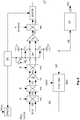
- the voltage signal TP [n] denotes the analog voltage signal to be read from the nth thermopile pixel connected to the inventive delta-sigma converter for evaluating a thermopile array.
- the successive feeding of such pixel signals takes place via the multiplexer AMUX.
- the voltage signal TP [n] together with the feedback signal S8 explained later, forms the differential input signal S0 (see SUB).
- SUB differential input signal
- the value of the difference input signal S0 results as the difference between the voltage signal TP [n] and the feedback signal S8.
- the input signal S0 is applied to a first multiplier M1.
- This first multiplier M1 multiplies the input signal S0 with a slow chopper signal A, which ultimately equates to a transformation of the frequencies of the analog voltage signal TP [n] in a higher frequency range (also referred to as “mixing up”).
- the slow (outer loop) chopper signal A typically changes its logical value when a thermopile line is changed and during half of the measurement period. This can preferably assume the values -1 and +1 here. Since the slow Chopper signal A is thus typically a digital signal, this first multiplier M1 is preferably implemented as a simple double switch that is switched with the aid of the slow digital chopper signal A.
- the evaluation of the logic states of the slow chopper signal A with -1 and 1 in conjunction with the sequence of values of the input signal S0, leads to the first signal S1, which results from the multiplication of S0 by the first multiplier M1.
- the first signal S1 is then applied to a second multiplier M2.
- This second multiplier M2 multiplies the first signal S1 by a second, fast chopper signal B, which results in a second signal S2.
- the second fast chopper signal B has a higher frequency than the slow chopper signal A.
- This second fast chopper signal B can also preferably assume the values -1 and +1 with regard to its effect on the first signal S1.
- the fast chopper signal B is thus also typically a digital signal.
- This second multiplier M2 can therefore also be implemented as a simple double changeover switch and can be changed over with the aid of the digital, fast chopper signal B.
- the evaluation of the logic states of the fast chopper signal B with -1 and 1 results again from the sequence of a change in state of the fast chopper signal B for the value of the second signal.
- the result is the second signal S2, which in turn can be interpreted as the first signal S1 ("mixing up") transformed in the frequency range.
- a transimpedance amplifier TV is connected to the output of the second multiplier M2 via the second signal S2 and amplifies the now double-modulated (double chopped or nested chopped) differential input signal S0 Current signals.
- the 1 / f noise behavior of the amplifier TV is advantageously used by the up-mixing, ie “chopping2” the signal S0, but this is known per se.
- a third multiplier M3 multiplies the third signal S3 by the fast chopper signal B.
- an inverted or negative fast chopper signal B could also be used, whereby in the first case it is used that a double exchange restores the original state and in the second case a swap back has the same effect. As a result, the signal S3 is mixed down; the fourth signal S4 arises.
- the output of the third multiplier M3 loads the differential integration capacitance consisting of the first individual capacitance C1 and the second individual capacitance C2 via the fourth signal S4.
- the current from the transimpedance amplifier TV is integrated in this differential integration capacitance C1, C2.
- the fourth signal S4 therefore preferably represents the integration of the third signal S3.
- a comparator CMP is connected to the output of the third multiplier M3 and the differential integration capacitance C1, C2 via the fourth signal S4.
- the comparator CMP now converts the fourth signal S4 into a one-bit data stream.
- the output of the comparator CMP, which supplies this one-bit data stream, is formed by the fifth signal S5, which, in contrast to the previous signals S1 to S4, is no longer differential.
- This fifth signal S5 is now passed from the output of the comparator CMP to the input of a fourth multiplier M4.
- the fourth multiplier M4 multiplies the fifth signal S5 by the said slow chopper signal A.
- the sign of the slow chopper signal A is negated or in the case of a digital slow chopper Signal A whose logic value is inverted.
- the fifth signal S5 is thus transformed back into the frequency range of the signal S0. Since both the fifth signal S5 and the slow chopper signal A are typically digital binary signals, the simplest form of implementation of the fourth multiplexer M4 is that of an EXOR gate. The result of this multiplication in the fourth multiplier M4 and thus its output represents the sixth signal S6.
- the subsequent controller ADCFB which receives the sixth signal S6, has two operating modes. In a first operating mode, the following digital-to-analog converter DAC is quickly brought close to the operating point; in the other mode, the controller ADCFB performs differentiation and integration, whereby the control loop receives the characteristics of a PID controller and thus "slower" works.
- the person skilled in the art is referred to the technical control literature with regard to the configuration and design of the loop filters for PID controllers.
- the controller ADCFB also converts the incoming one-bit signal, that is to say the sixth signal S6, into a data bus with six bits, namely into the seventh signal SB.
- the seventh signal SB forms the output of the controller ADCFB.
- the controller ADCFB is connected via this seventh signal SB both to a digital output filter DF and to a digital-to-analog converter DAC.
- the digital output filter DF again converts the bus width from 6-bit, the seventh signal SB, into the target bus width of the output signal Out, this output signal Out also being the output signal of the digital output filter DF at the same time.
- the digital-to-analog converter DAC converts the seventh signal SB into the analog feedback signal S8, which is finally connected as a differential signal with the voltage signal TP [n] of the nth to the inventive delta-sigma ADC for evaluating a thermopile array Thermopile forms the input signal S0. This closes the control loop.
- the logic circuit in ADCFB ensures that the control loop is stable.
- the aim of the multiplications in the first to fourth multipliers M1, M2, M3, M4 is the following Operations, here it is the transimpedance amplification in the transimpedance amplifier TV, the integration in the differential capacitor C1, C2 and the evaluation in the comparator CMP, to be carried out in a frequency range in which the noise and / or interference spectrum is less pronounced and thus to increase the conversion quality .
- Two multiplications in the first multiplier M1 and second multiplier M2 virtually transform the useful signal from the frequencies of the input signal S0 to higher frequencies, and the two multiplications in the third multiplier M3 and fourth multiplier M4 perform the corresponding reverse transformation.
- the first multiplier M1 and the fourth multiplier M4 therefore form a first multiplier pair and the second multiplier M2 and the third multiplier M3 form a second multiplier pair.
- Each pair thus consists of a preceding multiplier for transforming up to a higher frequency and a following multiplier for transforming back to the original frequency.
- the second pair of multipliers encompasses the transimpedance amplifier stage like a bracket.
- the frequency of the fast chopper signal B is therefore chosen according to the noise spectrum of this stage.
- the first multiplier pair includes the second multiplier pair and the transimpedance amplifier TV encompassed by it, in addition, the differential integration capacitance C1, C2 and the comparator CMP.
- the first frequency of the associated control signal of the first multiplier pair that of the slow chopper signal A.
- the first frequency of the slow chopper signal A is based on the line frequency with which the thermopile lines are read out.
- the particular advantage of the solution presented here is therefore that the chopping comprises the entire quantizer and the inverse transformation by the fourth multiplication in the fourth multiplier M4 only takes place after the comparator CMP.
- the low-pass characteristic of the integration stage which is essentially caused by the differential integration capacitance C1, C2 in interaction with the output resistance of the transimpedance amplifier TV, serves as a decimation filter for the second pair of multipliers M2, M3.
- the chopping ie the forward and backward transformations by the said multiplier pairs, thus reduces the noise and the offsets in the sixth signal S6.
- the main difference compared to the prior art is the implementation of the first multiplication in the first multiplier M1 directly at the input and the implementation of the last multiplication in the fourth multiplier M4 after the quantizer, i.e. the comparator CMP.
- the slow chopper signal A has a lower first frequency than the cutoff frequency of the low pass of the differential integration capacitor C1, C2 in combination with the differential output internal resistance of the transimpedance amplifier TV and the cutoff frequency of this low pass is again lower than the second frequency the fast chopper signal B.
- the delta-sigma converter according to the invention must find a suitable operating point very quickly.
- the ADCFB controller switches to another operating mode. This mode is typically only used for a short time. Therefore, the slow chopper signal A can be assumed to be static during this time.
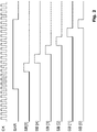
- the mode is in Fig. 2 characterized by the activation of an exemplary internal signal SAR.
- the MSB of the digital-to-analog converter DAC is set via the corresponding multi-bit line on which the seventh signal SB is present. If the value of the sixth signal S6, which is a 1-bit signal, is not flipped, ie not changed, as a result the MSB is retained. Otherwise it will be deleted again. Then the next less significant bit of the seventh signal SB is set and so on until the last bit, the LSB, has been evaluated. This starting value determination is quick and less precise. Therefore, after it has been completed, a switch is made to the already mentioned PID filtering (slower operating mode), the determined value of the seventh signal SB forming the start value for the controller ADCFB.
- PID filtering slower operating mode
- the integration capacitors C1, C2 of the low-pass filter are expediently also discharged at the beginning of a readout interval.
- This discharge control as well as the switching between the operating modes of the ADCFB controller and the row or column switching of the thermopile pixel array via the AMUX is carried out by the central control unit SE (see Fig. 1 ).
- control unit controls two transistors T1, T2, which ensures a discharge of both capacitors C1, C2. This discharge process takes place before the actual read-out process of the next thermopile pixel.
- the Fig. 2 also shows the system cycle CK, which expresses the speed of finding the operating point with this method. If the operating point were not set in this way, the circuit would not be able to cope with the requirements and would be too slow. After the operating point has been set, the delta-sigma converter works in the said PID mode and is then slower but more precise compared to the previous operating point search that took place at the beginning of a new readout interval.
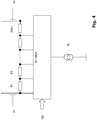
- Fig. 4 shows the offset compensation in the transimpedance amplifier TV.
- the offset is then corrected in a manner similar to that above.
- the offset in the transimpedance amplifier is set by asymmetrically feeding the current from the current source of the input differential stage into the same.
- the current is fed in via a 1: N multiplexer, where N indicates the number of possible feed positions.
- the two branches of the differential input stage are connected by a series connection of N-1 resistors which are typically of the same type and preferably have the same or a similar temperature coefficient as the resistances of the voltage reference typically present in the circuit.
- the N: 1 multiplexer now connects the current source to one of the resulting connection points between the N-1 resistors, the external points in this exemplary embodiment also being able to be selected as the feed point by the multiplexer.
- the device according to the invention has only a few analog circuit parts and very many digital circuit parts, which is an advantage. Due to the simplicity of the circuit, it only requires a very small area in a monolithic integrated circuit. It is therefore possible to provide such a delta-sigma converter for each thermopile pixel of a line and to switch it over only line by line. Each column of a thermopile array is therefore preferably assigned to a delta-sigma converter.
- a 32x32 thermopile pixel array would then have 32 inventive delta-sigma converters, each of which is connected via a 32: 1 analog multiplexer AMUX with exactly one thermopile pixel in a thermopile pixel line that is currently being processed. If the analog multiplexer AMUX switches from one line to the next, the slow chopper signal A also toggles.
- the 6-bit digital-to-analog converter DAC is implemented, for example, in such a way that a current is impressed into a resistor cascade with 63 identical resistors and the respective voltage is selected as the feedback signal S8 via a 64: 1 multiplexer.
- This has the advantage that all 32 delta-sigma converters assigned to the 32 columns of an exemplary 32x32 thermopile array can use the same resistor chain made up of 63 identical resistors, which considerably improves the matching from pixel to pixel.
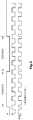
- Fig. 3 shows a clock scheme based on the digital system clock CK for the fast chopper signal B and the slow chopper signal A. It is important that the edges of the slow chopper signal A and the fast chopper signal B should not overlap if possible. Overlapping the edges would lead to interference. Therefore, the edges of the slow chopper signal A are preferably positioned in the pulse center of a pulse of the fast chopper signal B.
- the second frequency of the slow chopper signal B is preferably at least a factor of 2 higher than the first frequency of the slow chopper signal A.
- the second frequency of the fast chopper signal B should be an even multiple of the first frequency of the slow chopper signal A.
- Fig. 5 an alternative circuit diagram of the delta-sigma converter according to the invention is shown, the same reference numerals being used as in FIG Fig. 1 .
- the difference of Figs. 1 and 5 consists in the discharge circuit for the capacitors C1 and C2 of the low-pass filter.
- the two capacitors are not completely discharged when reading the next thermopile pixel. Rather takes place in the embodiment according to Fig. 5 a compensation of a potential charge difference between the two capacitors C1 and C2.
- the capacitors C1, C2 are decoupled from the signal lines by controlling the two transistors T1 and T2 and, in this state, are connected to one another via a transistor T3 so that the charge equalization can take place.
- the transistor T3 is then blocked and the two transistors T1 and T2 switched to the conductive state, so that both capacitors C1 and C2 carry the same electrical charge at the beginning of the next readout interval.
- thermopile pixel array With regard to the sequence of reading out different analog signals and their conversion into digital signals, the invention is of course not limited to reading out several pixels of an array. It is also possible according to the invention to read out one and the same pixel or one and the same detector successively one after the other in individual readout intervals in order to convert the analog readout signal, as described above, into a digital signal.
- the invention is of course not restricted to pixel arrays. Rather, what is decisive for the invention is that the transducer successively in readout intervals that are one behind the other Analog signals (be it voltage or current signals) are fed in. Whether these analog signals ultimately originate from one and the same pixel or successively from the pixels of an array is irrelevant for the invention.
- thermopile is not limited to use in a thermopile.
- Other IR radiation detectors such as bolometers, PIR etc. are also conceivable. It is also irrelevant to the invention whether these IR radiation detectors supply analog current or voltage signals. It is also possible for the IR radiation detector to be supplied with operating energy in order to deliver an analog signal at its output which represents the received IR radiation. In this respect, IR radiation detectors can be used which deliver an output signal without the supply of electrical energy, as is the case, for example, with PIR and with thermopiles.
Landscapes
- Engineering & Computer Science (AREA)
- Theoretical Computer Science (AREA)
- Analogue/Digital Conversion (AREA)
- Transforming Light Signals Into Electric Signals (AREA)
- Compression, Expansion, Code Conversion, And Decoders (AREA)
- Photometry And Measurement Of Optical Pulse Characteristics (AREA)
- Radiation Pyrometers (AREA)
Claims (8)
- Procédé de conversion d'un signal analogique (TP[i]), comme par exemple un signal de lecture en tension d'un pixel thermopile ou d'un pixel d'un autre détecteur sensible au rayonnement, en un signal numérique multi-bits (SB), avec les étapes suivantes :- délivrance successive de signaux analogiques (TP[i]) de grandeurs différentes à l'entrée d'un convertisseur Delta-Sigma pour la durée d'intervalles de lecture respectifs, à l'intérieur desquels les signaux analogiques respectifs (TP[i]) restent sensiblement inchangés,- création d'un signal numérique multi-bits (SB) correspondant à un signal analogique par le convertisseur Delta-Sigma avec un convertisseur analogique-numérique 1 bit sous forme d'un quantificateur (CMP) et avec un régulateur (ADCFB) commuté en série avec celui-ci, à la sortie duquel le signal numérique multi-bits (SB) est présent,- conversion du signal numérique multi-bits par un convertisseur numérique-analogique multi-bits (DAC) en un signal de rétroaction analogique (S8),- création d'un signal différentiel (S0) à partir du signal analogique (TP[i]) et du signal de rétroaction analogique (S8),- multiplication de ce signal différentiel (S0) par un premier signal de hachage (A) comportant une première fréquence afin de créer un premier signal différentiel (S1),- multiplication de ce premier signal différentiel (S1) par un deuxième signal de hachage (B) comportant une deuxième fréquence pour créer un deuxième signal différentiel (S2), dans lequel la deuxième fréquence est supérieure à la première fréquence,- amplification de ce deuxième signal différentiel (S2) afin de créer un troisième signal différentiel (S3),- multiplication de ce troisième signal différentiel (S3) par le deuxième signal de hachage (B) afin de créer un quatrième signal différentiel (S4),- filtrage passe-bas de ce quatrième signal différentiel (S4) au moyen d'un filtre passe-bas (C1, C2) et délivrance du quatrième signal différentiel (S4) filtré passe-bas à l'entrée du quantificateur ;- émission d'un cinquième signal différentiel (S5) par le quantificateur ;- multiplication de ce cinquième signal différentiel (S5) par un premier signal de hachage inversé (A) afin de créer un sixième signal différentiel (S6),- délivrance de ce sixième signal différentiel (S6) au régulateur (ADCFB) afin de créer le signal numérique multi-bits ; et- émission du signal numérique multi-bits (SB) le cas échéant après un filtrage numérique (DF),- dans lequel le régulateur (ADCFB) fonctionne sélectivement dans un premier mode et dans un deuxième mode,- dans lequel le régulateur (ADCFB) régule les déviations valeur nominale/valeur réelle entre le signal analogique (TP[i]) et le signal de rétroaction analogique (S8) plus rapidement dans son premier mode de fonctionnement que dans son deuxième mode de fonctionnement,- dans lequel le régulateur (ADCFB) fonctionne dans son premier mode de fonctionnement dans une phase initiale de l'intervalle de lecture pour une transformation du signal numérique multi-bits (SB) en signal analogique la plus rapide possible et- dans lequel le régulateur (ADCFB) fonctionne dans son deuxième mode de fonctionnement après la phase initiale de l'intervalle de lecture et pour le reste de la durée de celui-ci.
- Procédé selon la revendication 1, caractérisé en ce que le filtre passe-bas (C1, C2) comporte au moins un condensateur, lequel est déchargé après la fin de l'intervalle de lecture et/ou au début de la phase initiale de l'intervalle de lecture suivant.
- Procédé selon la revendication 1, caractérisé en ce que le filtre passe-bas (C1, C2) comporte deux condensateurs couplés avec respectivement une autre de ses entrées et en ce qu'après la fin de l'intervalle de lecture et/ou au début de la phase initiale de l'intervalle de lecture suivant une différence potentielle de charge entre les condensateurs est compensée ou éliminée.
- Procédé selon l'une des revendications 1 à 3, caractérisé en ce qu'un réseau de pixels thermopiles est préparé, lequel comporte plusieurs lignes de pixels respectivement dotées de plusieurs pixels, et en ce que les signaux de lecture des pixels de chaque ligne sont lus simultanément, à savoir respectivement selon les étapes de procédé selon l'une des revendications précédentes, et en ce qu'une commutation successive est effectuée de ligne en ligne afin de lire le réseau de pixels thermopiles.
- Dispositif destiné à la conversion d'un signal analogique (TP[i]), comme par exemple un signal de lecture en tension d'un pixel thermopile ou d'un pixel d'un autre détecteur sensible au rayonnement, en un signal numérique multi-bits (SB), doté :- d'un convertisseur Delta-Sigma, à l'entrée duquel peuvent être délivrés des signaux analogiques (TP[i]) de grandeurs différentes pour la durée d'intervalles de lecture respectifs, à l'intérieur desquels les signaux analogiques respectifs (TP[i]) restent sensiblement inchangés,- dans lequel le convertisseur Delta-Sigma comporte, afin de créer un signal numérique multi-bits (SB) correspondant à un signal analogique, un convertisseur analogique-numérique 1 bit sous forme d'un quantificateur (CMP) et un régulateur (ADCFB) commuté en série avec celui-ci, à la sortie duquel le signal numérique multi-bits (SB) peut être émis,- d'un convertisseur numérique-analogique multi-bits (DAC) destiné à convertir le signal de régulateur multi-bits en un signal de rétroaction analogique (S8),- d'une unité de soustraction (M1) destinée à créer un signal différentiel (S0) à partir du signal analogique (TP[i]) et du signal de rétroaction analogique (S8),- d'un multiplicateur (M1) destiné à la multiplication de ce signal différentiel (S0) par un premier signal de hachage (A) comportant une première fréquence afin de créer un premier signal différentiel (S1),- d'un multiplicateur (M2) destiné à la multiplication de ce premier signal différentiel (S1) par un deuxième signal de hachage (B) comportant une deuxième fréquence pour créer un deuxième signal différentiel (S2), dans lequel la deuxième fréquence est supérieure à la première fréquence,- d'un amplificateur (TV) destiné à amplifier ce deuxième signal différentiel (S2) afin de créer un troisième signal différentiel (S3),- d'un multiplicateur (M3) destiné à la multiplication de ce troisième signal différentiel (S3) par le deuxième signal de hachage (B) afin de créer un quatrième signal différentiel (S4),- d'un filtre passe-bas (C1, C2) destiné au filtrage passe-bas de ce quatrième signal différentiel (S4) et à délivrer le quatrième signal différentiel (S4) filtré passe-bas à l'entrée du quantificateur, dans lequel le quantificateur est réalisé pour l'émission d'un cinquième signal différentiel (S5),- d'un multiplicateur (M4) destiné à la multiplication de ce cinquième signal différentiel (S5) par un premier signal de hachage inversé (A) afin de créer un sixième signal différentiel (S6), lequel peut être délivré au régulateur (ADCFB) afin de créer le signal numérique multi-bits (SB), et- d'une unité de commande (SE) destinée à commander au moins le régulateur (ADCFB),- dans lequel le régulateur (ADCFB) peut fonctionner sélectivement dans un premier mode et dans un deuxième mode,- dans lequel les déviations valeur nominale/valeur réelle entre le signal analogique (TP[i]) et le signal de rétroaction analogique (S8) peuvent être régulées plus rapidement dans le premier mode de fonctionnement du régulateur (ADCFB) que dans le deuxième mode de fonctionnement de celui-ci,- dans lequel le régulateur (ADCFB) peut fonctionner dans son premier mode de fonctionnement dans une phase initiale de l'intervalle de lecture pour une transformation du signal numérique multi-bits (SB) en signal analogique la plus rapide possible et- dans lequel le régulateur (ADCFB) peut fonctionner dans son deuxième mode de fonctionnement après la phase initiale de l'intervalle de lecture et pour le reste de la durée de celui-ci.
- Dispositif selon la revendication 5, caractérisé en ce que le filtre passe-bas (C1, C2) comporte au moins un condensateur, lequel peut être déchargé après la fin de l'intervalle de lecture et/ou au début de la phase initiale de l'intervalle de lecture suivant.
- Dispositif selon la revendication 5, caractérisé en ce que le filtre passe-bas (C1, C2) comporte deux condensateurs couplés avec respectivement une autre de ses entrées et en ce qu'après la fin de l'intervalle de lecture et/ou au début de la phase initiale de l'intervalle de lecture suivant une différence potentielle de charge entre les condensateurs peut être compensée ou éliminée.
- Dispositif selon l'une des revendications 5 à 7, caractérisé en ce que le capteur comporte au moins une ligne dotée de plusieurs pixels, en ce que les signaux de lecture des pixels peuvent être lus simultanément par ligne.
Applications Claiming Priority (4)
| Application Number | Priority Date | Filing Date | Title |
|---|---|---|---|
| EP14168470 | 2014-05-15 | ||
| EP15155410 | 2015-02-17 | ||
| EP15162245 | 2015-04-01 | ||
| PCT/EP2015/060571 WO2015173293A1 (fr) | 2014-05-15 | 2015-05-13 | Numérisation rapide à consommation de courant réduite, traitement et filtrage de signaux analogiques d'un capteur ou détecteur |
Publications (2)
| Publication Number | Publication Date |
|---|---|
| EP3143697A1 EP3143697A1 (fr) | 2017-03-22 |
| EP3143697B1 true EP3143697B1 (fr) | 2021-09-08 |
Family
ID=53175061
Family Applications (1)
| Application Number | Title | Priority Date | Filing Date |
|---|---|---|---|
| EP15721729.0A Active EP3143697B1 (fr) | 2014-05-15 | 2015-05-13 | Numérisation rapide à consommation de courant réduite, traitement et filtrage de signaux analogiques d'un capteur ou détecteur |
Country Status (3)
| Country | Link |
|---|---|
| EP (1) | EP3143697B1 (fr) |
| CN (2) | CN205195692U (fr) |
| WO (1) | WO2015173293A1 (fr) |
Families Citing this family (1)
| Publication number | Priority date | Publication date | Assignee | Title |
|---|---|---|---|---|
| CN116488657A (zh) * | 2023-06-20 | 2023-07-25 | 南方电网数字电网研究院有限公司 | 积分器电路、西格玛-德尔塔调制器及模数转换器 |
Family Cites Families (5)
| Publication number | Priority date | Publication date | Assignee | Title |
|---|---|---|---|---|
| US6535153B1 (en) * | 1999-02-04 | 2003-03-18 | Med-El Electromedizinische Gerate Ges.M.B.H. | Adaptive sigma-delta modulation with one-bit quantization |
| DE102004030812B4 (de) * | 2004-02-27 | 2006-01-05 | Infineon Technologies Ag | Stromsparender Multibit-Delta-Sigma-Wandler |
| WO2007054895A1 (fr) * | 2005-11-11 | 2007-05-18 | Nxp B.V. | Circuit de traitement du signal comprenant un convertisseur analogique vers numérique de type sigma delta |
| US7474247B1 (en) * | 2007-09-26 | 2009-01-06 | Medtronic, Inc. | Detecting overloading of an analog-to-digital converter of an implantable medical device |
| US7714757B2 (en) * | 2007-09-26 | 2010-05-11 | Medtronic, Inc. | Chopper-stabilized analog-to-digital converter |
-
2015
- 2015-05-13 EP EP15721729.0A patent/EP3143697B1/fr active Active
- 2015-05-13 WO PCT/EP2015/060571 patent/WO2015173293A1/fr not_active Ceased
- 2015-05-15 CN CN201520316407.5U patent/CN205195692U/zh not_active Expired - Lifetime
- 2015-05-15 CN CN201510249436.9A patent/CN105306061B/zh active Active
Also Published As
| Publication number | Publication date |
|---|---|
| EP3143697A1 (fr) | 2017-03-22 |
| CN105306061A (zh) | 2016-02-03 |
| CN205195692U (zh) | 2016-04-27 |
| HK1215623A1 (zh) | 2016-09-02 |
| CN105306061B (zh) | 2019-12-24 |
| WO2015173293A1 (fr) | 2015-11-19 |
Similar Documents
| Publication | Publication Date | Title |
|---|---|---|
| DE69417296T2 (de) | Schaltung zur Verarbeitung von Signalen mit einer Eingangsstufe mit veränderbarer Verstärkung | |
| EP1603139B1 (fr) | Appareil et procédé pour compenser des erreurs dans un circuit d'échantillonnage et de maintien | |
| DE4127078C2 (de) | Phasenentzerrer für einen Digital/Analog-Wandler | |
| DE69809870T2 (de) | Delta-Sigma Pulsbreitenmodulator | |
| DE69325523T2 (de) | Analog-Digital-Wandler | |
| DE69131099T2 (de) | Analog-digitalwandler | |
| DE69117794T2 (de) | Mehrstufiger sigma-delta-Analog-zu-Digitalkonverter | |
| DE69123388T2 (de) | Analog-Digitalumsetzer | |
| DE4127096A1 (de) | Gleichspannungs-kalibriereinrichtung fuer einen digital/analog-wandler | |
| DE102021116136A1 (de) | Neues verfahren für eine schnelle erkennung und eine automatische verstärkungsanpassung in einem adc-basierten signal | |
| DE102019112542A1 (de) | Reservoirkondensator-basierter analog-digital-wandler | |
| DE102021132279A1 (de) | Schaltung einschliesslich eines strom-digital-analogwandlers, verfahren zum betreiben eines strom-digital-analog-wandlers und zeitkontinuierlicher delta-sigma-wandler | |
| DE102021114503A1 (de) | Neuartige programmierbare chopping-architektur zum reduzieren eines offsets in einem analogen front-end | |
| EP0736977B1 (fr) | Procédé d'autocalibrage d'un convertisseur analogique-numérique ou d'un convertisseur numérique-analogique | |
| DE102021102068B4 (de) | Vorrichtung mit einer kapazitiven Abtaststruktur, Verfahren zur Rauschreduzierung in einer Abtaststruktur, Vorrichtung mit einer Abtaststruktur, Vorrichtung, die zur Unterdrückung oder zum Ausgleich von skaliertem thermischen Rauschen in einer Umsetzphase aus einer Aufnahme des skalierten thermischen Rauschens in einer Erfassungsphase eingerichtet ist, Verfahren zur Unterdrückung oder zum Ausgleich von skaliertem thermischen Rauschen | |
| EP3143697B1 (fr) | Numérisation rapide à consommation de courant réduite, traitement et filtrage de signaux analogiques d'un capteur ou détecteur | |
| DE19742064A1 (de) | Analog-Digital-Umsetzverfahren und Vorrichtung zu seiner Ausführung | |
| DE102004005081B4 (de) | Pipeline-Analog/Digital-Wandler | |
| DE69707666T2 (de) | Flächeneffizientes Rekonstruktionsfilter, insbesondere für stromgesteuerte D/A-Wandler | |
| EP3141877A2 (fr) | Dispositif et procédé de fonctionnement de capteurs à infrarouge passif | |
| DE3130476C2 (fr) | ||
| DE69901037T2 (de) | Verzögerungskompensation des a/d wandlers in sigma-delta modulatoren | |
| EP0162314A1 (fr) | Convertisseur analogique-numérique | |
| EP0444234B1 (fr) | Procédé et dispositif de conversion analogique/numérique | |
| DE60021733T2 (de) | Verfahren zur analogischen dezimation von bildsignalen |
Legal Events
| Date | Code | Title | Description |
|---|---|---|---|
| STAA | Information on the status of an ep patent application or granted ep patent |
Free format text: STATUS: THE INTERNATIONAL PUBLICATION HAS BEEN MADE |
|
| PUAI | Public reference made under article 153(3) epc to a published international application that has entered the european phase |
Free format text: ORIGINAL CODE: 0009012 |
|
| STAA | Information on the status of an ep patent application or granted ep patent |
Free format text: STATUS: REQUEST FOR EXAMINATION WAS MADE |
|
| 17P | Request for examination filed |
Effective date: 20161115 |
|
| AK | Designated contracting states |
Kind code of ref document: A1 Designated state(s): AL AT BE BG CH CY CZ DE DK EE ES FI FR GB GR HR HU IE IS IT LI LT LU LV MC MK MT NL NO PL PT RO RS SE SI SK SM TR |
|
| AX | Request for extension of the european patent |
Extension state: BA ME |
|
| DAV | Request for validation of the european patent (deleted) | ||
| DAX | Request for extension of the european patent (deleted) | ||
| STAA | Information on the status of an ep patent application or granted ep patent |
Free format text: STATUS: EXAMINATION IS IN PROGRESS |
|
| 17Q | First examination report despatched |
Effective date: 20200626 |
|
| RAP1 | Party data changed (applicant data changed or rights of an application transferred) |
Owner name: ELMOS SEMICONDUCTOR SE |
|
| GRAP | Despatch of communication of intention to grant a patent |
Free format text: ORIGINAL CODE: EPIDOSNIGR1 |
|
| STAA | Information on the status of an ep patent application or granted ep patent |
Free format text: STATUS: GRANT OF PATENT IS INTENDED |
|
| INTG | Intention to grant announced |
Effective date: 20210326 |
|
| GRAS | Grant fee paid |
Free format text: ORIGINAL CODE: EPIDOSNIGR3 |
|
| GRAA | (expected) grant |
Free format text: ORIGINAL CODE: 0009210 |
|
| STAA | Information on the status of an ep patent application or granted ep patent |
Free format text: STATUS: THE PATENT HAS BEEN GRANTED |
|
| AK | Designated contracting states |
Kind code of ref document: B1 Designated state(s): AL AT BE BG CH CY CZ DE DK EE ES FI FR GB GR HR HU IE IS IT LI LT LU LV MC MK MT NL NO PL PT RO RS SE SI SK SM TR |
|
| REG | Reference to a national code |
Ref country code: GB Ref legal event code: FG4D Free format text: NOT ENGLISH |
|
| REG | Reference to a national code |
Ref country code: CH Ref legal event code: EP Ref country code: AT Ref legal event code: REF Ref document number: 1429495 Country of ref document: AT Kind code of ref document: T Effective date: 20210915 |
|
| REG | Reference to a national code |
Ref country code: DE Ref legal event code: R096 Ref document number: 502015015166 Country of ref document: DE |
|
| REG | Reference to a national code |
Ref country code: IE Ref legal event code: FG4D Free format text: LANGUAGE OF EP DOCUMENT: GERMAN |
|
| REG | Reference to a national code |
Ref country code: LT Ref legal event code: MG9D |
|
| REG | Reference to a national code |
Ref country code: NL Ref legal event code: MP Effective date: 20210908 |
|
| PG25 | Lapsed in a contracting state [announced via postgrant information from national office to epo] |
Ref country code: FI Free format text: LAPSE BECAUSE OF FAILURE TO SUBMIT A TRANSLATION OF THE DESCRIPTION OR TO PAY THE FEE WITHIN THE PRESCRIBED TIME-LIMIT Effective date: 20210908 Ref country code: ES Free format text: LAPSE BECAUSE OF FAILURE TO SUBMIT A TRANSLATION OF THE DESCRIPTION OR TO PAY THE FEE WITHIN THE PRESCRIBED TIME-LIMIT Effective date: 20210908 Ref country code: NO Free format text: LAPSE BECAUSE OF FAILURE TO SUBMIT A TRANSLATION OF THE DESCRIPTION OR TO PAY THE FEE WITHIN THE PRESCRIBED TIME-LIMIT Effective date: 20211208 Ref country code: BG Free format text: LAPSE BECAUSE OF FAILURE TO SUBMIT A TRANSLATION OF THE DESCRIPTION OR TO PAY THE FEE WITHIN THE PRESCRIBED TIME-LIMIT Effective date: 20211208 Ref country code: LT Free format text: LAPSE BECAUSE OF FAILURE TO SUBMIT A TRANSLATION OF THE DESCRIPTION OR TO PAY THE FEE WITHIN THE PRESCRIBED TIME-LIMIT Effective date: 20210908 Ref country code: HR Free format text: LAPSE BECAUSE OF FAILURE TO SUBMIT A TRANSLATION OF THE DESCRIPTION OR TO PAY THE FEE WITHIN THE PRESCRIBED TIME-LIMIT Effective date: 20210908 Ref country code: RS Free format text: LAPSE BECAUSE OF FAILURE TO SUBMIT A TRANSLATION OF THE DESCRIPTION OR TO PAY THE FEE WITHIN THE PRESCRIBED TIME-LIMIT Effective date: 20210908 Ref country code: SE Free format text: LAPSE BECAUSE OF FAILURE TO SUBMIT A TRANSLATION OF THE DESCRIPTION OR TO PAY THE FEE WITHIN THE PRESCRIBED TIME-LIMIT Effective date: 20210908 |
|
| PG25 | Lapsed in a contracting state [announced via postgrant information from national office to epo] |
Ref country code: LV Free format text: LAPSE BECAUSE OF FAILURE TO SUBMIT A TRANSLATION OF THE DESCRIPTION OR TO PAY THE FEE WITHIN THE PRESCRIBED TIME-LIMIT Effective date: 20210908 Ref country code: GR Free format text: LAPSE BECAUSE OF FAILURE TO SUBMIT A TRANSLATION OF THE DESCRIPTION OR TO PAY THE FEE WITHIN THE PRESCRIBED TIME-LIMIT Effective date: 20211209 |
|
| PG25 | Lapsed in a contracting state [announced via postgrant information from national office to epo] |
Ref country code: IS Free format text: LAPSE BECAUSE OF FAILURE TO SUBMIT A TRANSLATION OF THE DESCRIPTION OR TO PAY THE FEE WITHIN THE PRESCRIBED TIME-LIMIT Effective date: 20220108 Ref country code: SM Free format text: LAPSE BECAUSE OF FAILURE TO SUBMIT A TRANSLATION OF THE DESCRIPTION OR TO PAY THE FEE WITHIN THE PRESCRIBED TIME-LIMIT Effective date: 20210908 Ref country code: SK Free format text: LAPSE BECAUSE OF FAILURE TO SUBMIT A TRANSLATION OF THE DESCRIPTION OR TO PAY THE FEE WITHIN THE PRESCRIBED TIME-LIMIT Effective date: 20210908 Ref country code: RO Free format text: LAPSE BECAUSE OF FAILURE TO SUBMIT A TRANSLATION OF THE DESCRIPTION OR TO PAY THE FEE WITHIN THE PRESCRIBED TIME-LIMIT Effective date: 20210908 Ref country code: PT Free format text: LAPSE BECAUSE OF FAILURE TO SUBMIT A TRANSLATION OF THE DESCRIPTION OR TO PAY THE FEE WITHIN THE PRESCRIBED TIME-LIMIT Effective date: 20220110 Ref country code: PL Free format text: LAPSE BECAUSE OF FAILURE TO SUBMIT A TRANSLATION OF THE DESCRIPTION OR TO PAY THE FEE WITHIN THE PRESCRIBED TIME-LIMIT Effective date: 20210908 Ref country code: NL Free format text: LAPSE BECAUSE OF FAILURE TO SUBMIT A TRANSLATION OF THE DESCRIPTION OR TO PAY THE FEE WITHIN THE PRESCRIBED TIME-LIMIT Effective date: 20210908 Ref country code: EE Free format text: LAPSE BECAUSE OF FAILURE TO SUBMIT A TRANSLATION OF THE DESCRIPTION OR TO PAY THE FEE WITHIN THE PRESCRIBED TIME-LIMIT Effective date: 20210908 Ref country code: CZ Free format text: LAPSE BECAUSE OF FAILURE TO SUBMIT A TRANSLATION OF THE DESCRIPTION OR TO PAY THE FEE WITHIN THE PRESCRIBED TIME-LIMIT Effective date: 20210908 Ref country code: AL Free format text: LAPSE BECAUSE OF FAILURE TO SUBMIT A TRANSLATION OF THE DESCRIPTION OR TO PAY THE FEE WITHIN THE PRESCRIBED TIME-LIMIT Effective date: 20210908 |
|
| REG | Reference to a national code |
Ref country code: DE Ref legal event code: R097 Ref document number: 502015015166 Country of ref document: DE |
|
| PLBE | No opposition filed within time limit |
Free format text: ORIGINAL CODE: 0009261 |
|
| STAA | Information on the status of an ep patent application or granted ep patent |
Free format text: STATUS: NO OPPOSITION FILED WITHIN TIME LIMIT |
|
| PG25 | Lapsed in a contracting state [announced via postgrant information from national office to epo] |
Ref country code: DK Free format text: LAPSE BECAUSE OF FAILURE TO SUBMIT A TRANSLATION OF THE DESCRIPTION OR TO PAY THE FEE WITHIN THE PRESCRIBED TIME-LIMIT Effective date: 20210908 |
|
| 26N | No opposition filed |
Effective date: 20220609 |
|
| PG25 | Lapsed in a contracting state [announced via postgrant information from national office to epo] |
Ref country code: SI Free format text: LAPSE BECAUSE OF FAILURE TO SUBMIT A TRANSLATION OF THE DESCRIPTION OR TO PAY THE FEE WITHIN THE PRESCRIBED TIME-LIMIT Effective date: 20210908 |
|
| REG | Reference to a national code |
Ref country code: CH Ref legal event code: PL |
|
| REG | Reference to a national code |
Ref country code: BE Ref legal event code: MM Effective date: 20220531 |
|
| GBPC | Gb: european patent ceased through non-payment of renewal fee |
Effective date: 20220513 |
|
| PG25 | Lapsed in a contracting state [announced via postgrant information from national office to epo] |
Ref country code: MC Free format text: LAPSE BECAUSE OF FAILURE TO SUBMIT A TRANSLATION OF THE DESCRIPTION OR TO PAY THE FEE WITHIN THE PRESCRIBED TIME-LIMIT Effective date: 20210908 Ref country code: LU Free format text: LAPSE BECAUSE OF NON-PAYMENT OF DUE FEES Effective date: 20220513 Ref country code: LI Free format text: LAPSE BECAUSE OF NON-PAYMENT OF DUE FEES Effective date: 20220531 Ref country code: IT Free format text: LAPSE BECAUSE OF FAILURE TO SUBMIT A TRANSLATION OF THE DESCRIPTION OR TO PAY THE FEE WITHIN THE PRESCRIBED TIME-LIMIT Effective date: 20210908 Ref country code: CH Free format text: LAPSE BECAUSE OF NON-PAYMENT OF DUE FEES Effective date: 20220531 |
|
| PG25 | Lapsed in a contracting state [announced via postgrant information from national office to epo] |
Ref country code: IE Free format text: LAPSE BECAUSE OF NON-PAYMENT OF DUE FEES Effective date: 20220513 |
|
| PG25 | Lapsed in a contracting state [announced via postgrant information from national office to epo] |
Ref country code: GB Free format text: LAPSE BECAUSE OF NON-PAYMENT OF DUE FEES Effective date: 20220513 Ref country code: BE Free format text: LAPSE BECAUSE OF NON-PAYMENT OF DUE FEES Effective date: 20220531 |
|
| P01 | Opt-out of the competence of the unified patent court (upc) registered |
Effective date: 20230525 |
|
| REG | Reference to a national code |
Ref country code: AT Ref legal event code: MM01 Ref document number: 1429495 Country of ref document: AT Kind code of ref document: T Effective date: 20220513 |
|
| PG25 | Lapsed in a contracting state [announced via postgrant information from national office to epo] |
Ref country code: AT Free format text: LAPSE BECAUSE OF NON-PAYMENT OF DUE FEES Effective date: 20220513 |
|
| PG25 | Lapsed in a contracting state [announced via postgrant information from national office to epo] |
Ref country code: HU Free format text: LAPSE BECAUSE OF FAILURE TO SUBMIT A TRANSLATION OF THE DESCRIPTION OR TO PAY THE FEE WITHIN THE PRESCRIBED TIME-LIMIT; INVALID AB INITIO Effective date: 20150513 |
|
| PG25 | Lapsed in a contracting state [announced via postgrant information from national office to epo] |
Ref country code: MK Free format text: LAPSE BECAUSE OF FAILURE TO SUBMIT A TRANSLATION OF THE DESCRIPTION OR TO PAY THE FEE WITHIN THE PRESCRIBED TIME-LIMIT Effective date: 20210908 Ref country code: CY Free format text: LAPSE BECAUSE OF FAILURE TO SUBMIT A TRANSLATION OF THE DESCRIPTION OR TO PAY THE FEE WITHIN THE PRESCRIBED TIME-LIMIT Effective date: 20210908 |
|
| PG25 | Lapsed in a contracting state [announced via postgrant information from national office to epo] |
Ref country code: TR Free format text: LAPSE BECAUSE OF FAILURE TO SUBMIT A TRANSLATION OF THE DESCRIPTION OR TO PAY THE FEE WITHIN THE PRESCRIBED TIME-LIMIT Effective date: 20210908 |
|
| PG25 | Lapsed in a contracting state [announced via postgrant information from national office to epo] |
Ref country code: MT Free format text: LAPSE BECAUSE OF FAILURE TO SUBMIT A TRANSLATION OF THE DESCRIPTION OR TO PAY THE FEE WITHIN THE PRESCRIBED TIME-LIMIT Effective date: 20210908 |
|
| PGFP | Annual fee paid to national office [announced via postgrant information from national office to epo] |
Ref country code: DE Payment date: 20250515 Year of fee payment: 11 |
|
| PGFP | Annual fee paid to national office [announced via postgrant information from national office to epo] |
Ref country code: FR Payment date: 20250521 Year of fee payment: 11 |
|
| REG | Reference to a national code |
Ref country code: DE Ref legal event code: R081 Ref document number: 502015015166 Country of ref document: DE Owner name: ELMOS SEMICONDUCTOR SE, DE Free format text: FORMER OWNER: ELMOS SEMICONDUCTOR SE, 44227 DORTMUND, DE |