EP0162314A1 - Convertisseur analogique-numérique - Google Patents
Convertisseur analogique-numérique Download PDFInfo
- Publication number
- EP0162314A1 EP0162314A1 EP85104925A EP85104925A EP0162314A1 EP 0162314 A1 EP0162314 A1 EP 0162314A1 EP 85104925 A EP85104925 A EP 85104925A EP 85104925 A EP85104925 A EP 85104925A EP 0162314 A1 EP0162314 A1 EP 0162314A1
- Authority
- EP
- European Patent Office
- Prior art keywords
- digital
- signal
- analog
- output
- integrator
- Prior art date
- Legal status (The legal status is an assumption and is not a legal conclusion. Google has not performed a legal analysis and makes no representation as to the accuracy of the status listed.)
- Withdrawn
Links
- 230000007423 decrease Effects 0.000 claims 2
- 230000003247 decreasing effect Effects 0.000 claims 1
- 238000010586 diagram Methods 0.000 description 3
- 230000000694 effects Effects 0.000 description 2
- 238000005259 measurement Methods 0.000 description 2
- 238000013139 quantization Methods 0.000 description 2
- 230000003111 delayed effect Effects 0.000 description 1
- 230000001681 protective effect Effects 0.000 description 1
- 230000001052 transient effect Effects 0.000 description 1
- 230000001960 triggered effect Effects 0.000 description 1
- 238000011144 upstream manufacturing Methods 0.000 description 1
Images


Classifications
-
- H—ELECTRICITY
- H03—ELECTRONIC CIRCUITRY
- H03M—CODING; DECODING; CODE CONVERSION IN GENERAL
- H03M1/00—Analogue/digital conversion; Digital/analogue conversion
- H03M1/12—Analogue/digital converters
- H03M1/50—Analogue/digital converters with intermediate conversion to time interval
- H03M1/504—Analogue/digital converters with intermediate conversion to time interval using pulse width modulation
Definitions
- the invention relates to an analog-digital converter according to the preamble of claim 1.
- a generic analog-to-digital converter is known (US Pat. No. 4,296,412), in which all bits of the digital output signal are fed to a single digital-to-analog converter, which generates a corresponding analog signal, which is used to convert the input signal to a fixed one Factor proportional signal is compared.
- a particular advantage of such a tracking analog-digital converter is the extremely fast "data refresh", which under normal operating conditions only takes one cycle period.
- the object of the invention is to provide a generic analog-digital converter, which compared to the be Known generic analog-digital converters with digital-analog converters of the same type achieve greater dynamics, but at least the same as long as the input signal is within the range in which it could also be processed by the known generic analog-digital converter implements with the same accuracy as the latter.
- the expansion of the dynamic should take place without loss of the fast "data refresh".
- Analog-digital converters according to the invention are particularly suitable for converting the output signal of a current or voltage converter, in particular one which can also serve measurement and protection purposes, since not only the undisturbed signal, which remains within a limited range, has high, for Measurement purposes can be implemented with sufficient accuracy, but also disturbances of large amplitude, such as occur in the event of short circuits, can be detected with sufficient accuracy at least for protective purposes.
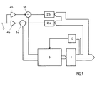
- the analog-digital converter shown in FIGS. 1 and 2 has a digital integrator 1 with a 16-bit output, a first 12-bit digital-analog converter 2a connected downstream of the integrator 1, a first subtractor 3a, which forms a first difference signal from the output signal of a first amplifier 4a, the input of which is connected to the input terminal 5 of the analog-digital converter and the output signal of the first digital-analog converter 2a, and a tracking circuit 6 connected upstream of the integrator 1 said first difference signal is supplied.
- the tracking circuit contains a differential discriminator 7 with a first discriminator 8a, which determines whether the signal at the input of the differential discriminator 7 lies between a first lower limit value -U and a first upper limit value + U a and if not, whether it is positive or negative .
- the absolute value U a of the limit values is somewhat above half of the voltage corresponding to a least significant bit.
- For the temporary storage of the two information are downstream of the first discriminator 8a are two D flip-flops 9, 9a which, like the integrator 1, are controlled by a clock generator 10.
- the integrator 1 is followed by a second 12-bit digital-to-analog converter 2b and a second subtractor 3b is provided, which results from the output signal of an amplifier 4b which is connected to the input terminal 5 and whose gain is one sixteenth of the gain of the first amplifier 4a , and the output signal of the second digital-to-analog converter 2b forms a second difference signal, which is also fed to the tracking circuit 6.
- the digital integrator 1 is designed as a four-stage cascade of 4-bit up-down counters 11a, b, c, d.
- the first digital-to-analog converter 2a are each supplied with the eleven bits with values 2 0 to 2 10 as amount bits and the polarity-determining most significant sixteenth bit, the second digital-to-analog converter 2b with the bits with values 2 4 to 2 14 as amount bits and also the most significant sixteenth.
- a feedback adder according to the prior art can also be used as the digital integrator.
- the tracking circuit 6 has an input selector switch 12 which can optionally apply the first or the second differential signal to the input of the differential discriminator 7.
- the differential discriminator 7 also has two further discriminators 8b, 8c designed as window discriminators, each of which determines whether the differential signal applied to its input between a second lower limit value -U b and a second upper limit value + U b or between a third lower limit value -U and a third upper limit + U c .
- the absolute values U b , U of the second and third limit values can be, for example, c 10 times and 150 times the voltage corresponding to a least significant bit, ie slightly more than half of the one bit with the significance 2 4 or . 2 8 corresponding voltages.
- D-flip-flops 9b, c which are controlled by clock generator 10, are also connected downstream of discriminators 8b, c for temporarily storing their output signals.
- Downstream of the differential discriminator 7 is a logic circuit 13, which of the output signals of the flip-flops 9a, 9b and 9c only forwards the signal with the highest priority to the integrator and blocks all signals of lower priority, 9c having the highest and 9a the lowest priority.
- an output selector switch 14 which can selectively output signals from the logic circuit 13 to the counting input of one of two successive 4-bit up-down counters of the integrator 1.
- the input selector switch 12 and the output selector switch 14 are controlled jointly by control logic 15 as a function of the output signals of the integrator 1.
- the control logic 15 contains a first EXOR gate 16, at the input of which the sixteenth and twelfth bits are located and whose output is connected to the inverting set input of a first D flip-flop 17 (for example SN 74 LS 74), at the clock input of which the output signal is one second EXOR gate 18, to which the polarity-determining sixteenth bit is supplied directly and once delayed by a second D flip-flop 19 by one clock period, and whose D input is at ground.
- a first EXOR gate 16 at the input of which the sixteenth and twelfth bits are located and whose output is connected to the inverting set input of a first D flip-flop 17 (for example SN 74 LS 74), at the clock input of which the output signal is one second EXOR gate 18, to which the polarity-determining sixteenth bit is supplied directly and once delayed by a second D flip-flop 19 by one clock period, and whose D input is at ground.
- the input selector switch 12 then applies the first differential signal, which is formed from the output signal of the first amplifier 4a and that of the first digital-to-analog converter 2a, to the input of the differential discriminator 7.
- the first discriminator 8a responds and generates a count signal which is stored in the flip-flop 9a on the next positive edge of the clock signal and, together with the polarity signal stored in the flip-flop 9, as a tracking signal via the logic circuit 13 and the output selector switch 14 reaches the first 4-bit up-down counter of integrator 1 as an up or down count signal and, on the next negative clock edge, has the effect that a least significant bit is added to or subtracted from the binary number at the output of the same.
- the second discriminator 8b responds and triggers a count signal, which comes directly to the count input of the second 4-bit up-down counter 11b and the addition or subtraction of a bit with the value 2 4 , corresponding to 16 times one least significant bit.
- a count signal simultaneously triggered by the first discriminator 8a is suppressed by the logic circuit 13.
- a count signal is passed to the count input of the third 4-bit up-down counter 11c and the addition of a bit with a value of 2 8 , corresponding to 256 times a least significant bit, is added or subtracted.
- the analog-digital converter for processing the output signal of a current or voltage converter important and sufficient qualitative correct reproduction of transient disturbances allowed for protection purposes.
- the bits from the fifth to the sixteenth are supplied to the second digital-to-analog converter 2b from the output of the integrator 1. These form a binary number which corresponds to the binary number formed by all the bits at the output of the integrator divided by sixteen, the remainder - the binary number formed by the four least significant bits, being eliminated. Since the output signal of the first amplifier 4a and that of the first digital-to-analog converter 2a are constantly adjusted, the output signal of the second amplifier 4b, which is in each case one sixteenth of the output signal of the first amplifier 4a and the output signal of the second digital-analogue -Converters 2b constantly compared.
- the output signal S 1 thus drops approximately in FIG. 3 represented in analog form - under -U + , so that the twelfth bit B 12 at the output of the integrator 1 assumes the value "0", so that is mastered with the first digital-to-analog converter 2a range exceeded.
- the output signal S 16 of the first EXOR gate 16 changes to "0" and, when passed to the inverting set input of the settable first D flip-flop 17, causes its output signal, which is also the output signal S 15 of the control logic 15, to "1" is set.
- the input selector switch 12 applies the second differential signal to the input of the differential discriminator 7.
- the output selector switch 14 is switched so that the counting signals emanating from the first discriminator 8a now reach the counting input of the second 4-bit up-down counter 11b and also that of the other discriminators 8b, c are redirected to the next higher 4-bit up-down counters llc and lld, which amounts to an enlargement of the tracking steps by 16 times, which is achieved by disregarding the first four bits the second digital-to-analog converter 20 caused division of the output number of the integrator 1 and the corresponding reduction of the analog signal, with which the divided output number is compared, compensated.
- the switchover described occurs within a clock period without additional loss of time. Although it leads to a 16-fold increase in the quantization error, it also has the consequence that a rapidly fluctuating input signal can be followed with 16 times larger tracking steps. Since the most important thing in many applications is the relative accuracy of the reproduction of the input signal, the first is hardly disadvantageous; On the other hand, often the rate of change occurring k nits of the input signal comply with the maximum occurring signal values, the second under certain circumstances is very advantageous.
- the value of the polarity-determining sixteenth bit changes. Since the output signal S 19 of the second D flip-flop 19 the same by one clock follows with a delay, the 'output signal S 18 of the second EXOR gate 18 changes to "1" and maintains this value for the duration of a clock period. Its positive edge has the effect that the output signal of the first D flip-flop 17, the D input of which is connected to ground, ie the output signal S 15 of the control logic 15 is set to "0". So zero acts as the lower switching limit.
- the differential discriminator 7 in turn becomes the output; signal of the first subtractor 3a supplied. Since the first most significant eleven bits and the most significant sixteenth were fed to the first digital-to-analog converter 2a all the time and the digital output signal was tracked with respect to the bits which are more significant than the fourth, the first digital-analog Pre-balanced converter 2a, ie the difference between the output signal of the first amplifier 4a and that of the first digital-analog converter 2a, as it appears at the output of the first subtractor 3a, normally has at most the order of magnitude of one bit of the value 2 4 during the switchover corresponding voltage.
- analog-digital converter can easily be expanded to more than two switching stages and its dynamics can be increased accordingly.
Landscapes
- Engineering & Computer Science (AREA)
- Theoretical Computer Science (AREA)
- Analogue/Digital Conversion (AREA)
Applications Claiming Priority (2)
| Application Number | Priority Date | Filing Date | Title |
|---|---|---|---|
| CH2378/84 | 1984-05-15 | ||
| CH237884 | 1984-05-15 |
Publications (1)
| Publication Number | Publication Date |
|---|---|
| EP0162314A1 true EP0162314A1 (fr) | 1985-11-27 |
Family
ID=4232378
Family Applications (1)
| Application Number | Title | Priority Date | Filing Date |
|---|---|---|---|
| EP85104925A Withdrawn EP0162314A1 (fr) | 1984-05-15 | 1985-04-23 | Convertisseur analogique-numérique |
Country Status (4)
| Country | Link |
|---|---|
| US (1) | US4590459A (fr) |
| EP (1) | EP0162314A1 (fr) |
| JP (1) | JPS60260230A (fr) |
| CA (1) | CA1241753A (fr) |
Families Citing this family (9)
| Publication number | Priority date | Publication date | Assignee | Title |
|---|---|---|---|---|
| JP2543177B2 (ja) * | 1989-03-24 | 1996-10-16 | 松下電器産業株式会社 | クランプ装置と自動利得制御装置 |
| US6044162A (en) * | 1996-12-20 | 2000-03-28 | Sonic Innovations, Inc. | Digital hearing aid using differential signal representations |
| US5995036A (en) * | 1998-03-17 | 1999-11-30 | Sonic Innovations, Inc. | Passive switched capacitor delta analog-to-digital converter with programmable gain control |
| US6445321B2 (en) | 1999-04-05 | 2002-09-03 | Sonic Innovations, Inc. | Hybrid low-pass sigma-delta modulator |
| US6163287A (en) * | 1999-04-05 | 2000-12-19 | Sonic Innovations, Inc. | Hybrid low-pass sigma-delta modulator |
| US6408318B1 (en) | 1999-04-05 | 2002-06-18 | Xiaoling Fang | Multiple stage decimation filter |
| JP4178702B2 (ja) * | 1999-12-28 | 2008-11-12 | ソニー株式会社 | 差動増幅器、コンパレータ、及びa/dコンバータ |
| US6313773B1 (en) | 2000-01-26 | 2001-11-06 | Sonic Innovations, Inc. | Multiplierless interpolator for a delta-sigma digital to analog converter |
| AU2001282120A1 (en) * | 2000-08-31 | 2002-03-13 | Fraunhofer-Gesellschaft Zur Forderung Der Angewandten Forschung E.V. | Method and device for converting an analog input signal into a sequence of digital output values |
Citations (2)
| Publication number | Priority date | Publication date | Assignee | Title |
|---|---|---|---|---|
| US3866131A (en) * | 1973-08-20 | 1975-02-11 | Coulter Electronics | Integerator system of wide range and pump circuit therefor |
| FR2443174A1 (fr) * | 1978-12-01 | 1980-06-27 | Bbc Brown Boveri & Cie | Procede et dispositif de transmission de signaux |
Family Cites Families (3)
| Publication number | Priority date | Publication date | Assignee | Title |
|---|---|---|---|---|
| US3786491A (en) * | 1972-07-05 | 1974-01-15 | Westinghouse Electric Corp | Digital integration apparatus and method |
| US4193066A (en) * | 1978-04-20 | 1980-03-11 | The United States Of America As Represented By The Secretary Of The Air Force | Automatic bias adjustment circuit for a successive ranged analog/digital converter |
| JPS5873231A (ja) * | 1981-10-27 | 1983-05-02 | Shimadzu Corp | Ad変換装置 |
-
1985
- 1985-04-23 EP EP85104925A patent/EP0162314A1/fr not_active Withdrawn
- 1985-05-07 CA CA000480959A patent/CA1241753A/fr not_active Expired
- 1985-05-14 US US06/733,878 patent/US4590459A/en not_active Expired - Fee Related
- 1985-05-15 JP JP60101660A patent/JPS60260230A/ja active Pending
Patent Citations (2)
| Publication number | Priority date | Publication date | Assignee | Title |
|---|---|---|---|---|
| US3866131A (en) * | 1973-08-20 | 1975-02-11 | Coulter Electronics | Integerator system of wide range and pump circuit therefor |
| FR2443174A1 (fr) * | 1978-12-01 | 1980-06-27 | Bbc Brown Boveri & Cie | Procede et dispositif de transmission de signaux |
Also Published As
| Publication number | Publication date |
|---|---|
| JPS60260230A (ja) | 1985-12-23 |
| CA1241753A (fr) | 1988-09-06 |
| US4590459A (en) | 1986-05-20 |
Similar Documents
| Publication | Publication Date | Title |
|---|---|---|
| DE69008360T2 (de) | Paralleler ad-wandler mit 2n-1-vergleichern. | |
| DE69015373T2 (de) | Digital-analog-wandler mit grossem dynamikbereich, hoher genauigkeit und hoher geschwindigkeit. | |
| EP0162315B1 (fr) | Convertisseur analogique-numérique | |
| DE2549626B2 (de) | Analog-Digital-Wandler | |
| DE10153309B4 (de) | Digital-Analog-Umsetzer-Vorrichtung mit hoher Auflösung | |
| DE2411062C3 (de) | Dynamisch vorgespannte Differentialverstärkeranordnung | |
| DE4320691C2 (de) | D/A-Wandler | |
| EP0162314A1 (fr) | Convertisseur analogique-numérique | |
| EP1250762B1 (fr) | Convertisseur analogique-numerique | |
| DE69510413T2 (de) | Komparator und Mehrfachvergleichs-A/D-Wandler unter Anwendung des Interpolationsprinzips | |
| DE3718937C2 (de) | Bipolarer A/D-Wandler mit automatischer Offsetkompensation | |
| DE2129383B2 (de) | Pulscodemodulator mit knickkennlinien-amplitudenwandler | |
| DE2618633C3 (de) | PCM-Decodierer | |
| EP0541878B1 (fr) | Convertisseur analogique/numérique Delta-Sigma | |
| EP0579025A2 (fr) | Convertisseur numérique-analogique à réseau capacitif pondéré | |
| EP0151769B1 (fr) | Convertisseur AN intégrable | |
| DE3689865T2 (de) | Gerät zur Umwandlung digitaler Werte in analoge Werte. | |
| DE3854845T2 (de) | Parallelvergleichstyp-AD-Wandler mit Fehlerunterdrückung | |
| DE69901037T2 (de) | Verzögerungskompensation des a/d wandlers in sigma-delta modulatoren | |
| CH647112A5 (de) | Schaltungsanordnung zur gewinnung einer zu der impulsdichte einer impulsfolge proportionalen steuerspannung. | |
| EP0149152A2 (fr) | Montage pour une commande numérique de niveau | |
| EP1445868B1 (fr) | Procédé pour conversion numérique-analogique et convertisseur numérique analogique | |
| DE3215519C2 (fr) | ||
| EP0158841A1 (fr) | Convertisseur analogique-numérique | |
| DE3734874C2 (fr) |
Legal Events
| Date | Code | Title | Description |
|---|---|---|---|
| PUAI | Public reference made under article 153(3) epc to a published international application that has entered the european phase |
Free format text: ORIGINAL CODE: 0009012 |
|
| AK | Designated contracting states |
Designated state(s): CH DE FR GB LI SE |
|
| 17P | Request for examination filed |
Effective date: 19860428 |
|
| RAP1 | Party data changed (applicant data changed or rights of an application transferred) |
Owner name: BBC BROWN BOVERI AG |
|
| 17Q | First examination report despatched |
Effective date: 19880919 |
|
| STAA | Information on the status of an ep patent application or granted ep patent |
Free format text: STATUS: THE APPLICATION IS DEEMED TO BE WITHDRAWN |
|
| 18D | Application deemed to be withdrawn |
Effective date: 19890128 |
|
| RIN1 | Information on inventor provided before grant (corrected) |
Inventor name: MASCHEK, MARTIN Inventor name: MASTNER, GEORG, DR. Inventor name: LANZ, OTTO, DR. |