EP3145035B1 - Anordnung zur herstellung einer elektrischen verbindung zwischen einem flachsteckerkontakt und einem hochstromleiter - Google Patents
Anordnung zur herstellung einer elektrischen verbindung zwischen einem flachsteckerkontakt und einem hochstromleiter Download PDFInfo
- Publication number
- EP3145035B1 EP3145035B1 EP16185486.4A EP16185486A EP3145035B1 EP 3145035 B1 EP3145035 B1 EP 3145035B1 EP 16185486 A EP16185486 A EP 16185486A EP 3145035 B1 EP3145035 B1 EP 3145035B1
- Authority
- EP
- European Patent Office
- Prior art keywords
- high current
- current conductor
- holding structure
- arrangement
- contacting
- Prior art date
- Legal status (The legal status is an assumption and is not a legal conclusion. Google has not performed a legal analysis and makes no representation as to the accuracy of the status listed.)
- Active
Links
Images


Classifications
-
- H—ELECTRICITY
- H01—ELECTRIC ELEMENTS
- H01R—ELECTRICALLY-CONDUCTIVE CONNECTIONS; STRUCTURAL ASSOCIATIONS OF A PLURALITY OF MUTUALLY-INSULATED ELECTRICAL CONNECTING ELEMENTS; COUPLING DEVICES; CURRENT COLLECTORS
- H01R13/00—Details of coupling devices of the kinds covered by groups H01R12/70 or H01R24/00 - H01R33/00
- H01R13/02—Contact members
-
- H—ELECTRICITY
- H01—ELECTRIC ELEMENTS
- H01R—ELECTRICALLY-CONDUCTIVE CONNECTIONS; STRUCTURAL ASSOCIATIONS OF A PLURALITY OF MUTUALLY-INSULATED ELECTRICAL CONNECTING ELEMENTS; COUPLING DEVICES; CURRENT COLLECTORS
- H01R13/00—Details of coupling devices of the kinds covered by groups H01R12/70 or H01R24/00 - H01R33/00
- H01R13/02—Contact members
- H01R13/15—Pins, blades or sockets having separate spring member for producing or increasing contact pressure
- H01R13/187—Pins, blades or sockets having separate spring member for producing or increasing contact pressure with spring member in the socket
-
- H—ELECTRICITY
- H01—ELECTRIC ELEMENTS
- H01R—ELECTRICALLY-CONDUCTIVE CONNECTIONS; STRUCTURAL ASSOCIATIONS OF A PLURALITY OF MUTUALLY-INSULATED ELECTRICAL CONNECTING ELEMENTS; COUPLING DEVICES; CURRENT COLLECTORS
- H01R13/00—Details of coupling devices of the kinds covered by groups H01R12/70 or H01R24/00 - H01R33/00
- H01R13/02—Contact members
- H01R13/10—Sockets for co-operation with pins or blades
- H01R13/11—Resilient sockets
- H01R13/113—Resilient sockets co-operating with pins or blades having a rectangular transverse section
-
- H—ELECTRICITY
- H01—ELECTRIC ELEMENTS
- H01R—ELECTRICALLY-CONDUCTIVE CONNECTIONS; STRUCTURAL ASSOCIATIONS OF A PLURALITY OF MUTUALLY-INSULATED ELECTRICAL CONNECTING ELEMENTS; COUPLING DEVICES; CURRENT COLLECTORS
- H01R13/00—Details of coupling devices of the kinds covered by groups H01R12/70 or H01R24/00 - H01R33/00
- H01R13/02—Contact members
- H01R13/22—Contacts for co-operating by abutting
-
- H—ELECTRICITY
- H01—ELECTRIC ELEMENTS
- H01R—ELECTRICALLY-CONDUCTIVE CONNECTIONS; STRUCTURAL ASSOCIATIONS OF A PLURALITY OF MUTUALLY-INSULATED ELECTRICAL CONNECTING ELEMENTS; COUPLING DEVICES; CURRENT COLLECTORS
- H01R13/00—Details of coupling devices of the kinds covered by groups H01R12/70 or H01R24/00 - H01R33/00
- H01R13/40—Securing contact members in or to a base or case; Insulating of contact members
- H01R13/42—Securing in a demountable manner
- H01R13/428—Securing in a demountable manner by resilient locking means on the contact members; by locking means on resilient contact members
- H01R13/434—Securing in a demountable manner by resilient locking means on the contact members; by locking means on resilient contact members by separate resilient locking means on contact member, e.g. retainer collar or ring around contact member
-
- H—ELECTRICITY
- H01—ELECTRIC ELEMENTS
- H01R—ELECTRICALLY-CONDUCTIVE CONNECTIONS; STRUCTURAL ASSOCIATIONS OF A PLURALITY OF MUTUALLY-INSULATED ELECTRICAL CONNECTING ELEMENTS; COUPLING DEVICES; CURRENT COLLECTORS
- H01R13/00—Details of coupling devices of the kinds covered by groups H01R12/70 or H01R24/00 - H01R33/00
- H01R13/46—Bases; Cases
-
- H—ELECTRICITY
- H01—ELECTRIC ELEMENTS
- H01R—ELECTRICALLY-CONDUCTIVE CONNECTIONS; STRUCTURAL ASSOCIATIONS OF A PLURALITY OF MUTUALLY-INSULATED ELECTRICAL CONNECTING ELEMENTS; COUPLING DEVICES; CURRENT COLLECTORS
- H01R13/00—Details of coupling devices of the kinds covered by groups H01R12/70 or H01R24/00 - H01R33/00
- H01R13/46—Bases; Cases
- H01R13/50—Bases; Cases formed as an integral body
-
- H—ELECTRICITY
- H01—ELECTRIC ELEMENTS
- H01R—ELECTRICALLY-CONDUCTIVE CONNECTIONS; STRUCTURAL ASSOCIATIONS OF A PLURALITY OF MUTUALLY-INSULATED ELECTRICAL CONNECTING ELEMENTS; COUPLING DEVICES; CURRENT COLLECTORS
- H01R13/00—Details of coupling devices of the kinds covered by groups H01R12/70 or H01R24/00 - H01R33/00
- H01R13/62—Means for facilitating engagement or disengagement of coupling parts or for holding them in engagement
- H01R13/627—Snap or like fastening
- H01R13/6275—Latching arms not integral with the housing
-
- H—ELECTRICITY
- H01—ELECTRIC ELEMENTS
- H01R—ELECTRICALLY-CONDUCTIVE CONNECTIONS; STRUCTURAL ASSOCIATIONS OF A PLURALITY OF MUTUALLY-INSULATED ELECTRICAL CONNECTING ELEMENTS; COUPLING DEVICES; CURRENT COLLECTORS
- H01R4/00—Electrically-conductive connections between two or more conductive members in direct contact, i.e. touching one another; Means for effecting or maintaining such contact; Electrically-conductive connections having two or more spaced connecting locations for conductors and using contact members penetrating insulation
- H01R4/26—Connections in which at least one of the connecting parts has projections which bite into or engage the other connecting part in order to improve the contact
-
- H—ELECTRICITY
- H01—ELECTRIC ELEMENTS
- H01R—ELECTRICALLY-CONDUCTIVE CONNECTIONS; STRUCTURAL ASSOCIATIONS OF A PLURALITY OF MUTUALLY-INSULATED ELECTRICAL CONNECTING ELEMENTS; COUPLING DEVICES; CURRENT COLLECTORS
- H01R4/00—Electrically-conductive connections between two or more conductive members in direct contact, i.e. touching one another; Means for effecting or maintaining such contact; Electrically-conductive connections having two or more spaced connecting locations for conductors and using contact members penetrating insulation
- H01R4/28—Clamped connections, spring connections
-
- H—ELECTRICITY
- H01—ELECTRIC ELEMENTS
- H01R—ELECTRICALLY-CONDUCTIVE CONNECTIONS; STRUCTURAL ASSOCIATIONS OF A PLURALITY OF MUTUALLY-INSULATED ELECTRICAL CONNECTING ELEMENTS; COUPLING DEVICES; CURRENT COLLECTORS
- H01R4/00—Electrically-conductive connections between two or more conductive members in direct contact, i.e. touching one another; Means for effecting or maintaining such contact; Electrically-conductive connections having two or more spaced connecting locations for conductors and using contact members penetrating insulation
- H01R4/28—Clamped connections, spring connections
- H01R4/48—Clamped connections, spring connections utilising a spring, clip, or other resilient member
-
- H—ELECTRICITY
- H01—ELECTRIC ELEMENTS
- H01R—ELECTRICALLY-CONDUCTIVE CONNECTIONS; STRUCTURAL ASSOCIATIONS OF A PLURALITY OF MUTUALLY-INSULATED ELECTRICAL CONNECTING ELEMENTS; COUPLING DEVICES; CURRENT COLLECTORS
- H01R4/00—Electrically-conductive connections between two or more conductive members in direct contact, i.e. touching one another; Means for effecting or maintaining such contact; Electrically-conductive connections having two or more spaced connecting locations for conductors and using contact members penetrating insulation
- H01R4/58—Electrically-conductive connections between two or more conductive members in direct contact, i.e. touching one another; Means for effecting or maintaining such contact; Electrically-conductive connections having two or more spaced connecting locations for conductors and using contact members penetrating insulation characterised by the form or material of the contacting members
Definitions
- the at least two positive locking elements which engage behind the contacting section can serve to securely fix the holding structure to the high current conductor. Furthermore, the at least two positive locking elements can serve as a counter-bearing for the high current conductor if at least one press-on element of the holding structure presses a tab contact disposed in the receptacle against the contacting section of the high current conductor.
- the holding structure has a plurality of positive locking elements.
- the high current conductor according to the invention is formed by the panel-shaped interface member such that a tab contact pressed against the latter can establish a good electrical contact with the high current conductor.
- the interface member can be formed such that a good contacting surface for the tab contact is produced.
- the at least one contacting element can also serve to give an improved electrical connection between the high current conductor and the tab contact.
- the at least one press-on element can be formed monolithically with the holding structure and can be deflected elastically away from the receptacle.
- the at least one press-on element can therefore be made like a spring.
- the monolithic configuration it is connected undetachably to the rest of the holding structure.
- the holding structure can thus be easy to produce.
- the elastic deflectability can lead to a tab contact being able to be repeatedly introduced into the receptacle and withdrawn from it again.
- the at least one press-on element can project at least partially into the receptacle.
- the at least one press-on element can be elastically deflected and thus be exposed to spring tension. In this way it can push against the tab contact or press the tab contact in the direction of the connection section or of a contacting section of a high current conductor disposed in the connection section.
- the holding structure has a plurality of press-on elements. In this way a high and even contact pressure onto the tab contact can be generated in the direction of the connection section.
- At least one press-on element can have a substantially elongated form, one end being connected securely to the holding structure so that a freely swinging leaf spring or a spring arm is formed.
- one longitudinal direction of this type of press-on element runs parallel to an insertion direction for a tab contact.
- the tab contact can then slide past the press-on element, by means of which the press-on element is deflected evenly. Since tab contacts are often formed from soft materials due to the good electrical conduction properties that are required, the described arrangement of the at least one press-on element can contribute to protecting the surface of the tab contact.
- the elongate press-on element can project, in particular with its free end, into the receptacle. On this free end the press-on element can be bent away from the receptacle so that a rounded structure is produced which can establish the contact with a tab contact with its rounded side. This can likewise contribute to protecting the surface of a tab contact.
- connection section In order to press a tab contact disposed in the receptacle particularly effectively in the direction of the connection section, in particular against a contacting section of a high current conductor disposed in the connection section, the connection section can lie opposite the at least one press-on element beyond the receptacle for the tab contact.
- the at least one positive locking element can be in the form of a latching means that can be deflected away from the connection section. In this way the at least one positive locking element can be released from the high current conductor again in a non-destructive manner.
- the holding structure can be able to be locked to the contacting section of the high current conductor along an assembly direction running substantially parallel to a direction of pressing on the press-on element.
- positive locking elements in the form of latching means can be used for the locking. Due to the possibility of locking, the holding structure can be connected quickly and easily to the high current conductor. Likewise, it may be possible to release the holding structure from the high current conductor again in a non-destructive manner if, for example, the high current conductor of the holding structure is to be replaced.
- the direction of pressing on the at least one press-on element runs transversely to an insertion direction for a tab contact. Consequently, the assembly direction also runs transversely to the insertion direction of the tab contact. In this way it can be guaranteed that upon introducing the tab contact into the receptacle or upon releasing the tab contact from the receptacle, the holding structure will not be separated from the high current conductor.
- the receptacle for the tab contact can have an insertion opening which opens at least the receptacle, preferably the common cavity, to the outside in the direction opposite the insertion direction or a plug-in direction for the tab contact.
- at least the receptacle is designed such that it only has an insertion opening for the tab contact and thus predetermines an insertion direction.
- the receptacle and the holding structure can be closed to other directions, and so incorrect insertion of the flat plug or insertion beyond a desired insertion position is prevented.
- the holding structure in the connection section can be at least partially open on its side lying opposite the at least one press-on element.
- the holding structure can have an assembly opening for the insertion of the high current conductor. If the holding structure has a common cavity, as described above, this common cavity is preferably accessible from the outside by means of the assembly opening.
- the holding structure can have at least one clamping element projecting at least partially into the receptacle and that can be deflected elastically from the latter in order to hold a tab contact by frictional bond.
- the clamping element can preferably be deflected transversely to the direction of pressing on.
- the at least one clamping element can rest against the narrow sides of a tab contact disposed in the receptacle in order to secure its position.
- the at least one clamping element can have latching elements which can engage in recesses in the tab contact formed to complement the latter.
- the at least one clamping element can project at least partially into the receptacle, at least if there is no tab contact disposed in the receptacle.
- the at least one clamping element is formed monolithically with the holding structure. It is particularly advantageous if the holding structure has two clamping elements lying opposite over the receptacle so that in an inserted state a tab contact is held between two clamping elements, at least with force closure.
- the holding structure in particular the at least one press-on element
- the at least one press-on element were in contrast made of a metallic material which was chosen with regard to electrical conductivity, there would be a risk of the at least one press-on element being plastically deformed over time. Materials with a high percentage of copper, for example, tend to creep over time, due to which the contact pressure dwindles. There is also a risk that with frequent deflection of the at least one press-on element, for example due to repeatedly introducing a tab contact into the receptacle, the at least one press-on element will lose its solidity.
- the at least one panel-shaped interface member can preferably be welded to the contacting section of the high current conductor. By welding the interface member to the high current conductor a secure and highly conductive connection between these parts can be generated. Alternatively or in addition, the panel-shaped interface member can also be connected to the high current conductor by soldering, crimping or riveting. Preferably, the panel-shaped interface member can be secured to the contacting section by laser welding.
- the contacting side can have at least one contacting element at least partially extending away from the interface member.
- the contacting element can be, for example, a projection which points from the contacting side in the direction of the receptacle.
- the contacting element can, for example, be made to be punctiform or rib-like.
- the at least one contacting element is in the form of a contact spring that can be deflected elastically towards the rest of the interface member.
- the at least one contacting element can therefore extend away from the contacting side of the panel-shaped interface member and be able to be deflected elastically towards the latter. This can be advantageous in order to contact a tab contact because, for example, small variations in the distance between the tab contact and the at least one interface member can be evened out.
- the high current conductor can have recesses which are formed to complement positive locking elements of a holding structure and can serve to receive these positive locking elements.
- the recesses can be arranged such that the positive locking elements arranged in them prevent movement of the holding structure along the high current conductor in a plane stretching parallel to a flat side of a tab contact.
- the compacted end of the high current conductor is made as a flat part. The recesses can then extend parallel to a plane stretching through and into the flat part.
- a high current conductor 1 according to the invention with a panel-shaped interface member 3 according to the invention is described by means of Fig. 1 .
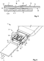
- Fig. 5 shows the high current conductor 1 according to the invention in a sectional illustration.
- the high current conductor 1 is preferably an earthing strap with a compacted end 5 as specified above.
- the high current conductor 1 can also be a bus bar or some other conductor. In the case of a bus bar the part of the latter to be contacted can already be sufficiently compact so that additional compacting is not necessarily required. The end 5 of the bus bar is then compacted per se.
- the panel-shaped interface member 3 lies on the contacting section 9 and is connected to the latter, by adhesive bond and/or with form locking.
- the interface member 3 is connected to the high current conductor 1 by laser welding.
- other types of connection are also possible.
- the interface member 3 can be soldered, riveted or crimped to the high current conductor 1. Combinations of these types of connection are also possible.
- the interface member 3 has a contacting side 13 which in the state connected to the high current conductor 1 points away from the compacted end 5.
- the contacting side 13 serves to contact a tab contact.
- the connection side 15 of the interface member 3 is located facing away from the contacting side 13. In the assembled state the connection side 15 lies on the compacted end 5 or the contacting section 9.
- the interface member 3 has positive locking elements 27 which can serve to position the interface member 3 on the compacted end 5 in order to secure the position during a fastening process, such as for example welding.
- the positive locking elements 27 are preferably disposed on the outer ends of the interface member 3. They extend away from the contacting side 13 and in the state fitted on the high current conductor 1 are disposed in the recesses 11. In this way displacement of the interface member 3 is effectively prevented both in the conduction direction L and transversely to this within the conductor plane 7.
- Fig. 2 shows a holding structure 29 according to the invention in a perspective illustration.
- the holding structure 29 can constitute an arrangement 31 according to the invention or be part of such an arrangement if the arrangement 31 includes additional components, for example an interface member 3.
- the holding structure 29 is preferably formed in one piece from a steel.
- the holding structure 29 has a connection section 33 for mounting the holding structure 29 to a contacting section 9 of a high current conductor 1 and a receptacle 35 for a tab contact.
- a receiving space 37 for the contacting section 9 of the high current conductor 1 can be disposed in the connection section 33.
- This receiving space 37 preferably forms with the receptacle 35 for the tab contact a common cavity 39.
- the holding structure 29 is preferably open on its side lying opposite the receptacle 35. The assembly opening 40 thus formed can facilitate connection to a high current conductor 1.
- the press-on elements 41 are preferably made in the form of spring arms, one free end 43 being deflectable and one base 45 being connected to the rest of the holding structure 29.
- a plurality of press-on elements 41 are disposed next to one another, the free ends 43 and the bases 45 of adjacent press-on elements 41 respectively alternating.
- the press-on elements 41 therefore have an alternating alignment.
- the holding structure 29 has an insertion opening 51 which clears the receptacle 35 for a tab contact.
- the receptacle 35 or the holding structure 29 has precisely one insertion opening 51 in order to predetermine a defined insertion direction E for a tab contact.
- the press-on elements 41 preferably run with their longitudinal directions 47 parallel to the insertion direction E.
- the holding structure can have a stop element 53 which can prevent a tab contact from being pushed through beyond a desired position in the receptacle 35. Furthermore, the stop element 53 can prevent a tab contact from being introduced into the holding structure 29 in a direction other than the insertion direction E.
- the holding structure 29 is shaped so that the direction of pressing on A and the insertion direction E run transversely to one another. It is also preferable if the direction of pressing in E and the direction of pressing on A run transversely to the conduction direction L of a high current conductor 1.
- the holding structure preferably respectively has another stop element 55 on both of the opposing ends. These stop elements 55 can also serve to prevent the introduction of a tab contact in a direction deviating from the insertion direction E.
- the stop elements 53 and 55 can additionally or alternatively also serve as spacers or as supports for the holding structure 29 on the contacting section 9. Therefore, with the stop elements 53 and 55 the holding structure 29 can be supported by the high current conductor 1 in the direction of pressing on A.
- the clamping elements 57 In order to hold a tab contact in the receptacle 35 more securely in the insertion direction E the clamping elements 57 have on free, deflectable ends 59 latching elements 61 which can engage in complementary recesses in a tab contact in order to additionally secure the latter in the insertion direction E.
- the clamping elements 57 with the latching elements 61 then constitute form limits for the tab contact.
- the clamping elements 57 can also serve to guide a tab contact during introduction into the receptacle 35.
- connection section 33 the holding structure 29 has mounting organ 63 which serve to fix the holding structure 29 to the contacting section 9 of the high current conductor 1.
- the mounting organ 63 are preferably made in the form of positive locking elements 65.
- the positive locking elements 65 are designed to engage behind the contacting section 9 of the high current conductor 1. For this purpose they initially run parallel to the direction of pressing on A and then have sections 67 which run transversely to the direction of pressing on A. 2 respective sections 67 which lie opposite one another in the insertion direction E point towards one another here.
- the connection section 33 is delimited in the direction of pressing on A by the sections 67. In a state fitted on the high current conductor 1 the high current conductor 1 or its contacting section 9 can rest against the sections 67.
- the holding structure 29 has two stationary positive locking elements 69 and two positive locking elements 65 which are in the form of elastically deflectable latching means 71.
- the two stationary positive locking elements 69 lie parallel to the insertion direction E here and the two positive locking elements 65 made in the form of latching means 71 also lie parallel to the insertion direction E.
- the latching means 71 can be deflected away from the connection section 33 transversely to the direction of pressing on A. Preferably, the latching means 71 can be deflected away from the connection section 33 parallel to the insertion direction E. By means of the elastic deflectability the sections 67 of the latching means 71 can be deflected away from the connection section 33 so that a high current conductor 1 can be inserted into the connection section 33. In order to insert a high current conductor 1 or in order to place the holding structure 29 on a high current conductor 1 a part of the high current conductor 1 can initially be inserted through the assembly opening 40 into the connection section 33, the fixed positive locking elements 69 engaging behind the latter.
- the part of the holding structure 29 which has the latching means 71 can be pressed against the high current conductor 1 so that the latching means 71 are deflected. In this way the high current conductor 1 can be moved into the connection section 33 and the latching means 71 can return to their initial position shown in Fig. 2 . All of the positive locking elements 65 of the holding structure 29 then engage behind the high current conductor 1. The high current conductor 1 can therefore be moved along an assembly direction M into the holding structure 29 which runs in the direction opposite the direction of pressing on A.
- Fig. 3 shows a holding structure 29 fitted on a contacting section 9 of a high current conductor 1.
- the high current conductor 1 corresponds to the embodiment described with reference to Fig. 1
- the holding structure 29 corresponds to the embodiment described with reference to Fig. 2 .
- the panel-shaped interface member 3 and the holding structure 29 are included in the embodiment of the arrangement 31 according to the invention.
- the holding structure 29 can in particular have been connected to the contacting section 9 in the way described with reference to Fig. 2 .
- the contacting section 9 is disposed in the connection section 33 of the holding structure 29.
- the positive locking elements 65 of the holding structure 29 engage behind the latter.
- the positive locking elements 65 are disposed here in the recesses 11 of the contacting section 9. In this way the holding structure 29 is prevented from becoming detached.
- the press-on elements 41 of the holding structure are disposed lying opposite the contacting elements 17 of the panel-shaped interface member 3 in the direction of pressing on A.
- the stop elements 53 and 55 rest against the high current conductor 1 so that the holding structure 29 is supported on the high current conductor 1 in the direction of pressing on A.
- these serve to prevent a tab contact from being introduced along a direction other than the insertion direction E.
- the receptacle 35 for a tab contact is now exclusively accessible through the insertion opening 51.
- Fig. 4 shows an arrangement 31 according to the invention as shown in Fig. 3 , but with indication of an inserted tab contact 73.
- Fig. 5 shows a cross-section along the section line marked as A-A in Fig. 4 .
- the tab contact 73 is disposed in the receptacle 35.
- the press-on elements 41 lie on its upper side 75 and the contacting elements 17 lie on its lower side 77.
- the press-on elements 41 generate a contact pressure in the direction of the connection section 33 by means of which the tab contact 73 is pressed against the panel-shaped interface member 3 in the direction of pressing on A. In this way an electrical contact is established between the tab contact and the high current conductor 1 via the contacting elements 17 or via the interface member 3.
- the arrangement 31 according to the invention may also consist purely of the holding structure 29.
- the panel-shaped interface member 3 constitutes an improvement of the arrangement 31 according to the invention, but is not necessarily required.
- the holding structure 29 has an insertion opening 51 which opens the receptacle 35 in the conduction direction L or in the direction opposite the insertion direction E. Towards the high current conductor 1 the holding structure has a stop element 53. On both of the ends lying transversely to the conduction direction L the holding structure 29 has two further stop elements 55 lying opposite one another.
- the press-on elements 41 are arranged with their longitudinal directions 47 parallel to the insertion direction E so as to also enable trouble-free introduction of a tab contact 73 in the second embodiment.
- the longitudinal directions one and 20 of the contact springs 19 of the panel-shaped interface member 3 are also aligned parallel to the insertion direction E.
Landscapes
- Details Of Connecting Devices For Male And Female Coupling (AREA)
- Connections Effected By Soldering, Adhesion, Or Permanent Deformation (AREA)
- Connection Of Batteries Or Terminals (AREA)
- Connector Housings Or Holding Contact Members (AREA)
- Coupling Device And Connection With Printed Circuit (AREA)
- Connection Or Junction Boxes (AREA)
Claims (14)
- Anordnung (31) zum Herstellen einer elektrischen Verbindung zwischen einem Flachkontakt (73) und einem Hochstrom-Leiter (1), wobei die Anordnung (31) eine Haltestruktur (29) aufweist, die einen Verbindungs-Abschnitt (33) mit wenigstens einem Anbringungsteil (63) zum Anbringen an einem Kontaktherstellungs-Abschnitt (9) des Hochstrom-Leiters (1) sowie eine Aufnahme (35) für den Flachkontakt (73) aufweist, die Haltestruktur (29) wenigstens ein Anpress-Element (41) aufweist, das so eingerichtet ist, dass es einen Kontaktdruck in der Richtung des Verbindungs-Abschnitts (33) entlang einer Press-Richtung (A) erzeugt, um den Flachkontakt (73) an einen in dem Verbindungs-Abschnitt (33) fixierten Hochstrom-Leiter (1) zu pressen, wobei die Press-Richtung (A) quer zu einer Einführungs-Richtung (E) für den Flachkontakt (73) verläuft und in dem Verbindungs-Abschnitt (33) ein Aufnahmeraum (37) für den Kontaktherstellungs-Abschnitt (9) des Hochstrom-Leiters (1) angeordnet ist, der mit der Aufnahme (35) für den Flachkontakt (73) einen gemeinsamen Hohlraum (39) bildet, dadurch gekennzeichnet, dass in dem Verbindungs-Abschnitt (33) die Haltestruktur (29) wenigstens zwei formschlüssig arretierende Elemente (65) aufweist, die hinter dem Kontaktherstellungs-Abschnitt (9) des Hochstrom-Leiters (1) in Eingriff kommen, wobei die wenigstens zwei formschlüssig arretierenden Elemente (65) zunächst parallel zu der Press-Richtung (A) verlaufen und dann jeweils einen Abschnitt (67) aufweisen, der quer zu dieser Richtung (A) verläuft, die Abschnitte (67) den Verbindungs-Abschnitt (33) in der Press-Richtung (A) begrenzen, und die Abschnitte (67) der wenigstens zwei formschlüssig arretierenden Elemente (65) in der Einführungs-Richtung (E) einander gegenüberliegen und aufeinander zu gerichtet sind.
- Anordnung (31) nach Anspruch 1, dadurch gekennzeichnet, dass das wenigstens eine Anpress-Element (41) aus einem Stück mit der Haltestruktur (29) ausgebildet ist und elastisch von der Aufnahme (35) weg gebogen werden kann.
- Anordnung (31) nach Anspruch 1 oder 2, dadurch gekennzeichnet, dass der Verbindungs-Abschnitt (33) dem wenigstens einen Anpress-Element (41) jenseits der Aufnahme (35) für den Flachkontakt (73) gegenüberliegt.
- Anordnung (31) nach einem der Ansprüche 1 bis 3, dadurch gekennzeichnet, dass das wenigstens eine formschlüssig arretierende Element (65) in Form einer Verriegelungseinrichtung (71) ausgebildet ist, die von dem Verbindungs-Abschnitt (33) weg gebogen werden kann.
- Anordnung (31) nach einem der Ansprüche 1 bis 4, dadurch gekennzeichnet, dass die Haltestruktur (29) an dem Kontaktherstellungs-Abschnitt (9) des Hochstrom-Leiters (1) in einer Montagerichtung (M) arretiert werden kann, die im Wesentlichen parallel zu einer Richtung (A) verläuft, in der das Anpress-Element (41) angepresst wird.
- Anordnung (31) nach einem der Ansprüche 1 bis 5, dadurch gekennzeichnet, dass die Haltestruktur (29) in dem Verbindungs-Abschnitt (33) an der Seite, die dem wenigstens einen Anpress-Element (41) gegenüberliegt, wenigstens teilweise offen ist.
- Anordnung (31) nach Anspruch 6, dadurch gekennzeichnet, dass in der Haltestruktur (29) eine Montageöffnung (40) für die Einführung des Hochstrom-Leiters (1) ausgebildet ist, über die der gemeinsame Hohlraum (39) von außen zugänglich ist.
- Anordnung (31) nach einem der Ansprüche 1 bis 7, dadurch gekennzeichnet, dass die Haltestruktur (29) wenigstens ein Klemmelement (57) aufweist, das wenigstens teilweise in die Aufnahme (35) hinein vorsteht und das senkrecht zu einer Richtung (A), in der das Anpress-Element (41) angepresst wird, elastisch aus der Aufnahme (35) heraus gebogen werden kann, um einen Flachkontakt (73) mittels Reibschluss zu halten.
- Anordnung (31) nach einem der Ansprüche 1 bis 8, dadurch gekennzeichnet, dass die Haltestruktur (29) in einem Stück aus Stahl geformt ist.
- Anordnung (31) nach einem der Ansprüche 1 bis 9, dadurch gekennzeichnet, dass die Anordnung (31) wenigstens ein plattenförmiges Grenzflächen-Element (3) mit einer Verbindungs-Seite (15) zur sicheren Verbindung mit dem Kontaktherstellungs-Abschnitt (9) des Hochstrom-Leiters (1) und mit einer Kontaktherstellungs-Seite (13) für die Herstellung von Kontakt mit einem in der Aufnahme (35) aufgenommenen Flachkontakt (73) umfasst.
- Anordnung (31) nach Anspruch 10, dadurch gekennzeichnet, dass die Kontaktherstellungs-Seite (13) wenigstens ein Kontaktherstellungs-Element (17) aufweist, das sich wenigstens teilweise von dem Grenzflächen-Element (3) weg erstreckt.
- Anordnung (31) nach Anspruch 11, dadurch gekennzeichnet, dass das wenigstens eine Kontaktherstellungs-Element (17) in Form einer Kontaktfeder (19) ausgeführt ist, die elastisch auf den übrigen Teil des Grenzflächen-Elementes (3) zu gebogen werden kann.
- Hochstrom-Leiter (1), insbesondere ein Erdungsband, der wenigstens ein verdichtetes Ende (5) aufweist, wobei das wenigstens eine verdichtete Ende (5) durch Reib- und/oder Haftschluss mit einem plattenförmigen Grenzflächen-Element (3) verbunden ist, das Grenzflächen-Element (3) eine von dem verdichteten Ende (5) weg gewandte Kontaktherstellungs-Seite (13) mit wenigstens einem Kontaktherstellungs-Element (17) hat, das sich wenigstens teilweise von dem Grenzflächen-Element (3) weg erstreckt, dadurch gekennzeichnet, dass das wenigstens eine verdichtete Ende (5) mit einer Anordnung (31) nach einem der Ansprüche 1 bis 12 versehen ist.
- Hochstrom-Leiter (1) nach Anspruch 13, dadurch gekennzeichnet, dass der Hochstromleiter (1) Aussparungen (11) zum Aufnehmen formschlüssig arretierender Elemente (27, 65) der Haltestruktur (29) und/oder des Grenzflächen-Elementes (3) aufweist.
Applications Claiming Priority (1)
| Application Number | Priority Date | Filing Date | Title |
|---|---|---|---|
| DE102015216632.5A DE102015216632A1 (de) | 2015-08-31 | 2015-08-31 | Anordnung zum Herstellen einer elektrischen Verbindung zwischen einem Flachkontakt und einem Hochstromleiter |
Publications (2)
| Publication Number | Publication Date |
|---|---|
| EP3145035A1 EP3145035A1 (de) | 2017-03-22 |
| EP3145035B1 true EP3145035B1 (de) | 2020-07-01 |
Family
ID=54697501
Family Applications (2)
| Application Number | Title | Priority Date | Filing Date |
|---|---|---|---|
| EP15195936.8A Not-in-force EP3136516B1 (de) | 2015-08-31 | 2015-11-23 | Verbinderanordnung mit einem klingenverbinder |
| EP16185486.4A Active EP3145035B1 (de) | 2015-08-31 | 2016-08-24 | Anordnung zur herstellung einer elektrischen verbindung zwischen einem flachsteckerkontakt und einem hochstromleiter |
Family Applications Before (1)
| Application Number | Title | Priority Date | Filing Date |
|---|---|---|---|
| EP15195936.8A Not-in-force EP3136516B1 (de) | 2015-08-31 | 2015-11-23 | Verbinderanordnung mit einem klingenverbinder |
Country Status (5)
| Country | Link |
|---|---|
| US (2) | US10218105B2 (de) |
| EP (2) | EP3136516B1 (de) |
| JP (2) | JP6839944B2 (de) |
| CN (2) | CN106486791B (de) |
| DE (1) | DE102015216632A1 (de) |
Families Citing this family (42)
| Publication number | Priority date | Publication date | Assignee | Title |
|---|---|---|---|---|
| DE102015216632A1 (de) * | 2015-08-31 | 2017-03-02 | Te Connectivity Germany Gmbh | Anordnung zum Herstellen einer elektrischen Verbindung zwischen einem Flachkontakt und einem Hochstromleiter |
| DE102016209478A1 (de) | 2016-05-31 | 2017-11-30 | Te Connectivity Germany Gmbh | Verbindungskäfig zur Verbindung zweier elektrischer Flachkontakte |
| DE102016221351A1 (de) * | 2016-10-28 | 2018-05-03 | Te Connectivity Germany Gmbh | Flachkontaktbuchse mit Ausleger |
| DE102016123081B4 (de) * | 2016-11-30 | 2018-06-14 | Amphenol-Tuchel Electronics Gmbh | Zylindrische Hochstromkontakt-Steckverbinder-Buchse |
| JP6787175B2 (ja) * | 2017-02-22 | 2020-11-18 | 株式会社オートネットワーク技術研究所 | 多接点型端子 |
| DE102017220185A1 (de) * | 2017-11-13 | 2019-05-16 | Te Connectivity Germany Gmbh | Buchsenkontakt |
| CN109802258B (zh) * | 2017-11-15 | 2022-01-25 | 富士康(昆山)电脑接插件有限公司 | 电连接器及其组合 |
| JP2019110074A (ja) * | 2017-12-20 | 2019-07-04 | 矢崎総業株式会社 | 接続端子及びコネクタ |
| JP2019185885A (ja) * | 2018-04-03 | 2019-10-24 | 矢崎総業株式会社 | 中継端子及び中継コネクタ |
| US10181673B1 (en) * | 2018-05-29 | 2019-01-15 | Te Connectivity Corporation | Receptacle terminal for a junction box |
| US10389055B1 (en) * | 2018-06-20 | 2019-08-20 | Delphia Technologies, Llc | Electrical connector assembly |
| FR3094578B1 (fr) * | 2019-04-01 | 2021-12-10 | Aptiv Tech Ltd | Dispositif de connexion de puissance pour batterie électrique et ensemble de connexion comprenant ce dispositif. |
| EP3783744B1 (de) * | 2019-08-23 | 2026-03-25 | Yazaki Europe Ltd. | Elektrische verbinderanordnung |
| JP7281087B2 (ja) * | 2019-11-01 | 2023-05-25 | 株式会社オートネットワーク技術研究所 | 端子接続構造 |
| CN110957597B (zh) * | 2019-12-27 | 2024-08-30 | 深圳乔合里科技股份有限公司 | 双簧片扁平大电流端子及其组装方法 |
| DE102020001379B3 (de) * | 2020-03-03 | 2021-08-19 | Wieland-Werke Aktiengesellschaft | Anordnung von Bauteilen zur Übertragung von elektrischem Strom |
| TWI789587B (zh) * | 2020-03-31 | 2023-01-11 | 映興電子股份有限公司 | 雙閘刀對接式連接器 |
| EP3896715B1 (de) * | 2020-04-14 | 2024-04-24 | Tyco Electronics France SAS | Halterung für eine schmelzsicherung die für eine lösbare kooperation mit einem stromleiterstab konfigiriert ist |
| US11128078B1 (en) * | 2020-07-20 | 2021-09-21 | TE Connectivity Services Gmbh | Current carrying retention clip |
| DE102020121969A1 (de) | 2020-08-21 | 2022-02-24 | Amphenol-Tuchel Electronics Gesellschaft mit beschränkter Haftung | Verriegelungszone für ein Steckkontaktelement |
| US11264752B1 (en) * | 2020-11-09 | 2022-03-01 | Aptiv Technologies Limited | Planar terminal connector having an additional contact spring |
| JP2022150224A (ja) * | 2021-03-26 | 2022-10-07 | 株式会社オートネットワーク技術研究所 | 端子ユニット,第1端子,第2端子 |
| DE102021112425A1 (de) | 2021-05-12 | 2022-11-17 | Te Connectivity Germany Gmbh | Vibrationsbelastbare elektrische Hochstrom-Flachbuchsenkontakteinrichtung |
| CN113258352B (zh) * | 2021-05-26 | 2022-11-29 | 宣城立讯精密工业有限公司 | 电性连接套件及电连接器 |
| CN113258372B (zh) * | 2021-05-26 | 2022-12-02 | 宣城立讯精密工业有限公司 | 电性连接套件及电性连接器 |
| CN113725663B (zh) * | 2021-08-25 | 2022-04-22 | 浙江普可医疗科技有限公司 | 一种传感器连接装置 |
| EP4406068A4 (de) * | 2021-09-22 | 2025-01-01 | Ennovi Industries, Inc. | Geneigter spulenkoppler |
| JP7884532B2 (ja) * | 2021-10-13 | 2026-07-03 | 古河電気工業株式会社 | メス型端子、コネクタ、端子付き電線、コネクタ付き電線及びワイヤーハーネス |
| KR102954731B1 (ko) * | 2021-11-18 | 2026-04-21 | 한국단자공업 주식회사 | 전자 부품용 커넥터 조립체 |
| EP4231460A1 (de) | 2022-02-17 | 2023-08-23 | Tyco Electronics France SAS | Kontaktelement, elektrischer verbinder und elektrische verbinderanordnung |
| JP2023172374A (ja) * | 2022-05-23 | 2023-12-06 | 古河電気工業株式会社 | メス型端子、端子付き電線、メス型コネクタ、コネクタ付き電線及びワイヤーハーネス |
| US20240204438A1 (en) * | 2022-12-20 | 2024-06-20 | Aptiv Technologies AG | High voltage electrical terminal with compliant contact insert |
| CN118352822A (zh) * | 2023-01-13 | 2024-07-16 | 泰科电子(上海)有限公司 | 端子、连接器和连接器组件 |
| DE102023101116A1 (de) * | 2023-01-18 | 2024-07-18 | Te Connectivity Solutions Gmbh | Vibrationsbelastbares elektrisches Flachbuchsenterminal |
| JP2024121499A (ja) * | 2023-02-27 | 2024-09-06 | 古河電気工業株式会社 | メス型端子、コネクタ、端子付き電線、コネクタ付き電線及びワイヤーハーネスならびにメス型端子の生産方法 |
| DE102024126223B3 (de) | 2024-09-12 | 2026-03-12 | Dinkle Electric Machinery (China) Co., Ltd. | Steckverbinderstruktur |
| TWI918130B (zh) | 2024-09-13 | 2026-03-11 | 貝爾威勒電子股份有限公司 | 母線連接器 |
| CN121886016A (zh) * | 2024-10-11 | 2026-04-17 | 泰科电子(上海)有限公司 | 连接器端子、电连接组件和连接器 |
| DE102024210639A1 (de) | 2024-11-06 | 2026-05-07 | Robert Bosch Gesellschaft mit beschränkter Haftung | Elektrisches Kabel mit Steckerkontur und Verfahren zur Herstellung einer Steckerkontur an einem elektrischen Kabel |
| DE102024004607A1 (de) | 2024-11-15 | 2026-05-21 | Dinkle Electric Machinery (China) Co., Ltd. | Mehrkontakt-anschlussstruktur |
| DE102024133494A1 (de) * | 2024-11-15 | 2026-05-21 | Dinkle Electric Machinery (China) Co., Ltd. | Mehrkontakt-anschlussstruktur und anschlussplatte davon |
| DE102024004608A1 (de) | 2024-11-15 | 2026-05-21 | Dinkle Electric Machinery (China) Co., Ltd. | Mehrkontakt-anschlussstruktur |
Family Cites Families (64)
| Publication number | Priority date | Publication date | Assignee | Title |
|---|---|---|---|---|
| US2997685A (en) * | 1956-06-05 | 1961-08-22 | Bryant Electric Co | Electrical connector |
| NL135884C (de) * | 1965-11-06 | |||
| DE1665132C3 (de) * | 1967-04-27 | 1975-09-25 | Multi-Contact Ag, Basel (Schweiz) | Elektrische Kontaktanordnung, insbesondere Hochstrom-Kontaktanordnung |
| DE3330984A1 (de) * | 1983-08-27 | 1985-03-14 | Licentia Patent-Verwaltungs-Gmbh, 6000 Frankfurt | Vorrichtung zum elektrisch leitenden verbinden von zwei oder mehreren elektrisch leitenden stiften |
| US5399098A (en) * | 1993-10-29 | 1995-03-21 | Molex Incorporated | Electrical connector and terminal therefor for mating with a blade contact |
| ES2117799T3 (es) * | 1994-07-27 | 1998-08-16 | United Technologies Automotive | Terminal electrico. |
| DE4433983A1 (de) * | 1994-09-23 | 1996-03-28 | Ackermann Albert Gmbh Co | Anschlußklemme für elektrische Installationen |
| US5588884A (en) * | 1995-09-08 | 1996-12-31 | Packard Hughes Interconnect Company | Stamped and formed contacts for a power connector |
| FR2740266B1 (fr) * | 1995-10-20 | 1997-11-28 | Cinch Connecteurs Sa | Dispositif de raccordement de deux languettes males d'organes de contacts electriques |
| US5911605A (en) * | 1997-10-16 | 1999-06-15 | Ui Automotive Dearborn, Inc. | Universal terminal connection |
| JPH11307159A (ja) * | 1998-04-16 | 1999-11-05 | Kansei Corp | 電気接続端子 |
| JP3783412B2 (ja) * | 1998-06-16 | 2006-06-07 | 住友電装株式会社 | 回路基板 |
| JP3736128B2 (ja) * | 1998-08-11 | 2006-01-18 | 株式会社日立製作所 | 多芯導体線及びその製造法 |
| JP2000243498A (ja) * | 1999-02-19 | 2000-09-08 | Furukawa Electric Co Ltd:The | 箱型雌端子 |
| EP1089387A3 (de) * | 1999-09-27 | 2001-12-19 | F.C.I. - Framatome Connectors International | Modulare elektrische Anschlussbuchse |
| CH694478A5 (de) * | 2000-01-20 | 2005-01-31 | Multi Holding Ag | Kontaktelement. |
| US6485337B2 (en) * | 2000-08-30 | 2002-11-26 | Delphi Technologies, Inc. | Electrical connector |
| US6860768B2 (en) * | 2000-09-15 | 2005-03-01 | Alcoa Fujikura Limited | Combination sleeve and spring cage incorporated into a one-piece female terminal for interengaging a corresponding male terminal and method of configuring such a sleeve and spring cage from a blank shape |
| US6264509B1 (en) * | 2001-01-10 | 2001-07-24 | Yazaki North America, Inc. | High cycle terminal with protected failsafe contact |
| US20030060090A1 (en) * | 2001-09-21 | 2003-03-27 | Allgood Christopher L. | High current automotive electrical connector and terminal |
| FR2830374B1 (fr) * | 2001-10-03 | 2004-09-10 | Framatome Connectors Int | Dispositif de connexion comportant un contact double, en particulier pour les applications en moyenne tension |
| EP1429424A1 (de) * | 2002-12-10 | 2004-06-16 | Meccanotecnica Codognese S.p.A. | Elektrisches Anschlussteil |
| CN2710203Y (zh) * | 2003-10-22 | 2005-07-13 | 莫列斯公司 | 卡缘连接器组合 |
| DE10351540B3 (de) * | 2003-11-03 | 2005-08-11 | Intedis Gmbh & Co. Kg | Flachsteckbuchse |
| JP2005196975A (ja) * | 2003-12-26 | 2005-07-21 | Jst Mfg Co Ltd | コネクタ |
| DE102004015345A1 (de) | 2004-03-30 | 2005-10-27 | Kostal Kontakt Systeme Gmbh | Elektrischer Steckhülsenkontakt für Hochstromanwendungen |
| CN2755810Y (zh) * | 2004-12-14 | 2006-02-01 | 富港电子(东莞)有限公司 | 记忆卡连接器 |
| DE102005043601B4 (de) * | 2005-09-12 | 2007-06-14 | Yazaki Europe Ltd., Hemel Hempstead | Kontakthalteklammer zur Montage an einer Stromschiene und Kontakthalterung aus diesen |
| US7241180B1 (en) | 2006-01-31 | 2007-07-10 | Medtronic, Inc. | Medical electrical lead connector assembly |
| DE102007016070A1 (de) * | 2007-04-03 | 2008-10-09 | Lear Corp., Southfield | Elektrische Anschlussanordnung und Verfahren zum Nutzen der elektrischen Anschlussanordnung |
| US7374460B1 (en) * | 2007-04-17 | 2008-05-20 | Traxxas Lp | Electrical connector assembly |
| ES2370849T3 (es) * | 2007-04-26 | 2011-12-23 | Multi-Holding Ag | Dispositivo de contacto para proporcionar un contacto eléctrico entre elementos conductores de corriente planos. |
| EP2048746B1 (de) * | 2007-08-13 | 2016-10-05 | Tyco Electronics Nederland B.V. | Stromschienenanschlusssystem |
| US7766706B2 (en) * | 2008-11-17 | 2010-08-03 | J. S. T. Corporation | Female terminal assembly with compression clip |
| JP5282540B2 (ja) * | 2008-11-21 | 2013-09-04 | 日立電線株式会社 | 雄雌接続構造 |
| JP5173777B2 (ja) * | 2008-12-15 | 2013-04-03 | 矢崎総業株式会社 | オス端子の構造 |
| EP2211425A1 (de) * | 2009-01-23 | 2010-07-28 | MTA S.p.A. | Elektrische Buchsenklemme |
| CN102414925B (zh) * | 2009-07-03 | 2015-05-27 | 矢崎总业株式会社 | 阴端子 |
| JP5381492B2 (ja) * | 2009-08-19 | 2014-01-08 | 住友電装株式会社 | 雌端子金具 |
| JP2011070897A (ja) * | 2009-09-25 | 2011-04-07 | Sumitomo Wiring Syst Ltd | レバー式コネクタ |
| KR101598633B1 (ko) * | 2009-11-11 | 2016-02-29 | 타이코에이엠피 주식회사 | 커넥터용 단자 |
| DE202010003555U1 (de) * | 2010-03-16 | 2010-07-08 | Rosenberger Hochfrequenztechnik Gmbh & Co. Kg | Hochstromsteckverbinder |
| JP2011210429A (ja) * | 2010-03-29 | 2011-10-20 | Aisin Aw Co Ltd | 電気的接続装置 |
| CH702863B1 (de) * | 2010-03-30 | 2014-12-15 | Multi Holding Ag | Verbindungselement. |
| DE202010010827U1 (de) * | 2010-07-29 | 2010-10-21 | Rosenberger Hochfrequenztechnik Gmbh & Co. Kg | Hochstromsteckverbinder |
| JP5632225B2 (ja) * | 2010-07-30 | 2014-11-26 | 矢崎総業株式会社 | 端子接続構造 |
| JP5083847B1 (ja) * | 2011-06-07 | 2012-11-28 | 日本航空電子工業株式会社 | コンタクトエレメント及びコネクタ |
| JP5723695B2 (ja) * | 2011-06-21 | 2015-05-27 | 矢崎総業株式会社 | 雌端子 |
| JP5723694B2 (ja) * | 2011-06-21 | 2015-05-27 | 矢崎総業株式会社 | 雌端子 |
| US8388389B2 (en) * | 2011-07-07 | 2013-03-05 | Tyco Electronics Corporation | Electrical connectors having opposing electrical contacts |
| DE102011085700A1 (de) | 2011-11-03 | 2013-05-08 | Bayerische Motoren Werke Aktiengesellschaft | Hochstrom-Steckverbinder für Kraftfahrzeuganwendungen |
| JP2013101795A (ja) * | 2011-11-08 | 2013-05-23 | Sumitomo Wiring Syst Ltd | 電流検出装置のバスバー接続構造 |
| US8821170B1 (en) * | 2012-07-19 | 2014-09-02 | Robert Hla Thein | Electrical contact having multiple cantilevered beams |
| JP6124074B2 (ja) * | 2013-03-21 | 2017-05-10 | 住友電装株式会社 | 雌端子 |
| US9070990B2 (en) * | 2013-05-21 | 2015-06-30 | Tyco Electronics Corporation | Power connector having opposing contact springs |
| DE202013103444U1 (de) * | 2013-07-31 | 2014-11-04 | Weidmüller Interface GmbH & Co. KG | Kontaktelement für eine Steckanordnung eines insbesondere außen geführten Bussystems |
| US10096865B2 (en) * | 2013-12-13 | 2018-10-09 | Hitachi Automotive Systems, Ltd. | Secondary cell module |
| JP6369029B2 (ja) * | 2014-01-28 | 2018-08-08 | オムロン株式会社 | コネクタ |
| DE102014001302A1 (de) * | 2014-01-31 | 2014-08-14 | Daimler Ag | Vorrichtung zur Befestigung eines elektrisch leitenden Kabelschuhs an einem externen elektrischen Kontaktelement |
| CN104037523B (zh) * | 2014-06-13 | 2016-05-11 | 四川永贵科技有限公司 | 一种大电流端子 |
| JP6591146B2 (ja) * | 2014-07-08 | 2019-10-16 | 日本航空電子工業株式会社 | コンタクト及びそれを備えるコネクタ |
| DE102015216632A1 (de) * | 2015-08-31 | 2017-03-02 | Te Connectivity Germany Gmbh | Anordnung zum Herstellen einer elektrischen Verbindung zwischen einem Flachkontakt und einem Hochstromleiter |
| US9893450B2 (en) * | 2015-09-25 | 2018-02-13 | Hirose Electric Co., Ltd. | Electrical connecting member and electrical connector having the same |
| DE102016201103B4 (de) * | 2016-01-26 | 2023-10-05 | Lisa Dräxlmaier GmbH | Kontaktteil |
-
2015
- 2015-08-31 DE DE102015216632.5A patent/DE102015216632A1/de active Pending
- 2015-11-23 EP EP15195936.8A patent/EP3136516B1/de not_active Not-in-force
-
2016
- 2016-08-24 EP EP16185486.4A patent/EP3145035B1/de active Active
- 2016-08-25 JP JP2016164218A patent/JP6839944B2/ja not_active Expired - Fee Related
- 2016-08-25 JP JP2016164249A patent/JP6783588B2/ja active Active
- 2016-08-30 CN CN201610773362.3A patent/CN106486791B/zh active Active
- 2016-08-30 CN CN201610771189.3A patent/CN106486806B/zh not_active Expired - Fee Related
- 2016-08-31 US US15/253,282 patent/US10218105B2/en active Active
- 2016-08-31 US US15/253,300 patent/US9793620B2/en not_active Expired - Fee Related
Non-Patent Citations (1)
| Title |
|---|
| None * |
Also Published As
| Publication number | Publication date |
|---|---|
| US20170062955A1 (en) | 2017-03-02 |
| EP3145035A1 (de) | 2017-03-22 |
| US20170062966A1 (en) | 2017-03-02 |
| JP6783588B2 (ja) | 2020-11-11 |
| EP3136516B1 (de) | 2018-06-20 |
| JP2017050281A (ja) | 2017-03-09 |
| CN106486791A (zh) | 2017-03-08 |
| CN106486806B (zh) | 2020-02-11 |
| JP2017054808A (ja) | 2017-03-16 |
| JP6839944B2 (ja) | 2021-03-10 |
| CN106486806A (zh) | 2017-03-08 |
| CN106486791B (zh) | 2021-09-03 |
| US10218105B2 (en) | 2019-02-26 |
| US9793620B2 (en) | 2017-10-17 |
| EP3136516A1 (de) | 2017-03-01 |
| DE102015216632A1 (de) | 2017-03-02 |
Similar Documents
| Publication | Publication Date | Title |
|---|---|---|
| EP3145035A1 (de) | Anordnung zur herstellung einer elektrischen verbindung zwischen einem flachsteckerkontakt und einem hochstromleiter | |
| JP7146842B2 (ja) | 導体接続端子 | |
| JP6665280B2 (ja) | 導体接続接点要素 | |
| US9847587B2 (en) | Spring-force terminal connection and plug connector | |
| US7252559B1 (en) | Two piece electrical terminal | |
| US8419486B2 (en) | Receptacle terminal with a contact spring | |
| EP3376598B1 (de) | Kontaktträger, elektrische kontakteinrichtung sowie verfahren zum herstellen eines konfektionierten kabels | |
| US10050400B2 (en) | Connection cage for connecting two electrical flat contacts | |
| EP2483969B1 (de) | Einteilige leitfähige klemme für einen einführungsdraht-stecker | |
| US20210184382A1 (en) | Terminal fitting | |
| CN102832510A (zh) | 屏蔽连接器 | |
| EP2228870A1 (de) | Elektrischer Verbinder | |
| JP5966041B1 (ja) | 分岐コネクタ | |
| KR102591645B1 (ko) | 커넥터 어셈블리 | |
| KR20050061581A (ko) | 편평 가요성 케이블용 커넥터 | |
| JP2016189329A (ja) | 分岐コネクタ | |
| CN113424369B (zh) | 保护导体接头 | |
| CN103208690B (zh) | 压接型连接器 | |
| KR102748963B1 (ko) | 전기 단자 | |
| KR101714402B1 (ko) | 저삽입력 소켓형 터미널 | |
| EP3324488B1 (de) | Verbinderanordnung mit leiterandrückelement | |
| KR101803796B1 (ko) | 전원전선 연결용 커넥터 | |
| KR20160053370A (ko) | 케이블 접속용 전기커넥터 | |
| KR101520927B1 (ko) | 터미널 | |
| EP2051332B1 (de) | Verbessertes Schnellanschluss-Endgerät |
Legal Events
| Date | Code | Title | Description |
|---|---|---|---|
| PUAI | Public reference made under article 153(3) epc to a published international application that has entered the european phase |
Free format text: ORIGINAL CODE: 0009012 |
|
| STAA | Information on the status of an ep patent application or granted ep patent |
Free format text: STATUS: THE APPLICATION HAS BEEN PUBLISHED |
|
| AK | Designated contracting states |
Kind code of ref document: A1 Designated state(s): AL AT BE BG CH CY CZ DE DK EE ES FI FR GB GR HR HU IE IS IT LI LT LU LV MC MK MT NL NO PL PT RO RS SE SI SK SM TR |
|
| AX | Request for extension of the european patent |
Extension state: BA ME |
|
| STAA | Information on the status of an ep patent application or granted ep patent |
Free format text: STATUS: REQUEST FOR EXAMINATION WAS MADE |
|
| 17P | Request for examination filed |
Effective date: 20170922 |
|
| RBV | Designated contracting states (corrected) |
Designated state(s): AL AT BE BG CH CY CZ DE DK EE ES FI FR GB GR HR HU IE IS IT LI LT LU LV MC MK MT NL NO PL PT RO RS SE SI SK SM TR |
|
| STAA | Information on the status of an ep patent application or granted ep patent |
Free format text: STATUS: EXAMINATION IS IN PROGRESS |
|
| 17Q | First examination report despatched |
Effective date: 20180319 |
|
| GRAP | Despatch of communication of intention to grant a patent |
Free format text: ORIGINAL CODE: EPIDOSNIGR1 |
|
| STAA | Information on the status of an ep patent application or granted ep patent |
Free format text: STATUS: GRANT OF PATENT IS INTENDED |
|
| INTG | Intention to grant announced |
Effective date: 20200218 |
|
| GRAS | Grant fee paid |
Free format text: ORIGINAL CODE: EPIDOSNIGR3 |
|
| GRAA | (expected) grant |
Free format text: ORIGINAL CODE: 0009210 |
|
| STAA | Information on the status of an ep patent application or granted ep patent |
Free format text: STATUS: THE PATENT HAS BEEN GRANTED |
|
| AK | Designated contracting states |
Kind code of ref document: B1 Designated state(s): AL AT BE BG CH CY CZ DE DK EE ES FI FR GB GR HR HU IE IS IT LI LT LU LV MC MK MT NL NO PL PT RO RS SE SI SK SM TR |
|
| REG | Reference to a national code |
Ref country code: CH Ref legal event code: EP Ref country code: AT Ref legal event code: REF Ref document number: 1287026 Country of ref document: AT Kind code of ref document: T Effective date: 20200715 |
|
| REG | Reference to a national code |
Ref country code: IE Ref legal event code: FG4D |
|
| REG | Reference to a national code |
Ref country code: DE Ref legal event code: R096 Ref document number: 602016039007 Country of ref document: DE |
|
| REG | Reference to a national code |
Ref country code: LT Ref legal event code: MG4D |
|
| PG25 | Lapsed in a contracting state [announced via postgrant information from national office to epo] |
Ref country code: BG Free format text: LAPSE BECAUSE OF FAILURE TO SUBMIT A TRANSLATION OF THE DESCRIPTION OR TO PAY THE FEE WITHIN THE PRESCRIBED TIME-LIMIT Effective date: 20201001 |
|
| REG | Reference to a national code |
Ref country code: NL Ref legal event code: MP Effective date: 20200701 |
|
| REG | Reference to a national code |
Ref country code: AT Ref legal event code: MK05 Ref document number: 1287026 Country of ref document: AT Kind code of ref document: T Effective date: 20200701 |
|
| PG25 | Lapsed in a contracting state [announced via postgrant information from national office to epo] |
Ref country code: FI Free format text: LAPSE BECAUSE OF FAILURE TO SUBMIT A TRANSLATION OF THE DESCRIPTION OR TO PAY THE FEE WITHIN THE PRESCRIBED TIME-LIMIT Effective date: 20200701 Ref country code: LT Free format text: LAPSE BECAUSE OF FAILURE TO SUBMIT A TRANSLATION OF THE DESCRIPTION OR TO PAY THE FEE WITHIN THE PRESCRIBED TIME-LIMIT Effective date: 20200701 Ref country code: CZ Free format text: LAPSE BECAUSE OF FAILURE TO SUBMIT A TRANSLATION OF THE DESCRIPTION OR TO PAY THE FEE WITHIN THE PRESCRIBED TIME-LIMIT Effective date: 20200701 Ref country code: PT Free format text: LAPSE BECAUSE OF FAILURE TO SUBMIT A TRANSLATION OF THE DESCRIPTION OR TO PAY THE FEE WITHIN THE PRESCRIBED TIME-LIMIT Effective date: 20201102 Ref country code: AT Free format text: LAPSE BECAUSE OF FAILURE TO SUBMIT A TRANSLATION OF THE DESCRIPTION OR TO PAY THE FEE WITHIN THE PRESCRIBED TIME-LIMIT Effective date: 20200701 Ref country code: ES Free format text: LAPSE BECAUSE OF FAILURE TO SUBMIT A TRANSLATION OF THE DESCRIPTION OR TO PAY THE FEE WITHIN THE PRESCRIBED TIME-LIMIT Effective date: 20200701 Ref country code: NO Free format text: LAPSE BECAUSE OF FAILURE TO SUBMIT A TRANSLATION OF THE DESCRIPTION OR TO PAY THE FEE WITHIN THE PRESCRIBED TIME-LIMIT Effective date: 20201001 Ref country code: GR Free format text: LAPSE BECAUSE OF FAILURE TO SUBMIT A TRANSLATION OF THE DESCRIPTION OR TO PAY THE FEE WITHIN THE PRESCRIBED TIME-LIMIT Effective date: 20201002 Ref country code: HR Free format text: LAPSE BECAUSE OF FAILURE TO SUBMIT A TRANSLATION OF THE DESCRIPTION OR TO PAY THE FEE WITHIN THE PRESCRIBED TIME-LIMIT Effective date: 20200701 Ref country code: SE Free format text: LAPSE BECAUSE OF FAILURE TO SUBMIT A TRANSLATION OF THE DESCRIPTION OR TO PAY THE FEE WITHIN THE PRESCRIBED TIME-LIMIT Effective date: 20200701 |
|
| PG25 | Lapsed in a contracting state [announced via postgrant information from national office to epo] |
Ref country code: PL Free format text: LAPSE BECAUSE OF FAILURE TO SUBMIT A TRANSLATION OF THE DESCRIPTION OR TO PAY THE FEE WITHIN THE PRESCRIBED TIME-LIMIT Effective date: 20200701 Ref country code: RS Free format text: LAPSE BECAUSE OF FAILURE TO SUBMIT A TRANSLATION OF THE DESCRIPTION OR TO PAY THE FEE WITHIN THE PRESCRIBED TIME-LIMIT Effective date: 20200701 Ref country code: LV Free format text: LAPSE BECAUSE OF FAILURE TO SUBMIT A TRANSLATION OF THE DESCRIPTION OR TO PAY THE FEE WITHIN THE PRESCRIBED TIME-LIMIT Effective date: 20200701 Ref country code: IS Free format text: LAPSE BECAUSE OF FAILURE TO SUBMIT A TRANSLATION OF THE DESCRIPTION OR TO PAY THE FEE WITHIN THE PRESCRIBED TIME-LIMIT Effective date: 20201101 |
|
| PG25 | Lapsed in a contracting state [announced via postgrant information from national office to epo] |
Ref country code: MC Free format text: LAPSE BECAUSE OF FAILURE TO SUBMIT A TRANSLATION OF THE DESCRIPTION OR TO PAY THE FEE WITHIN THE PRESCRIBED TIME-LIMIT Effective date: 20200701 Ref country code: NL Free format text: LAPSE BECAUSE OF FAILURE TO SUBMIT A TRANSLATION OF THE DESCRIPTION OR TO PAY THE FEE WITHIN THE PRESCRIBED TIME-LIMIT Effective date: 20200701 |
|
| REG | Reference to a national code |
Ref country code: CH Ref legal event code: PL |
|
| REG | Reference to a national code |
Ref country code: DE Ref legal event code: R097 Ref document number: 602016039007 Country of ref document: DE |
|
| PG25 | Lapsed in a contracting state [announced via postgrant information from national office to epo] |
Ref country code: DK Free format text: LAPSE BECAUSE OF FAILURE TO SUBMIT A TRANSLATION OF THE DESCRIPTION OR TO PAY THE FEE WITHIN THE PRESCRIBED TIME-LIMIT Effective date: 20200701 Ref country code: CH Free format text: LAPSE BECAUSE OF NON-PAYMENT OF DUE FEES Effective date: 20200831 Ref country code: SM Free format text: LAPSE BECAUSE OF FAILURE TO SUBMIT A TRANSLATION OF THE DESCRIPTION OR TO PAY THE FEE WITHIN THE PRESCRIBED TIME-LIMIT Effective date: 20200701 Ref country code: RO Free format text: LAPSE BECAUSE OF FAILURE TO SUBMIT A TRANSLATION OF THE DESCRIPTION OR TO PAY THE FEE WITHIN THE PRESCRIBED TIME-LIMIT Effective date: 20200701 Ref country code: LU Free format text: LAPSE BECAUSE OF NON-PAYMENT OF DUE FEES Effective date: 20200824 Ref country code: LI Free format text: LAPSE BECAUSE OF NON-PAYMENT OF DUE FEES Effective date: 20200831 Ref country code: EE Free format text: LAPSE BECAUSE OF FAILURE TO SUBMIT A TRANSLATION OF THE DESCRIPTION OR TO PAY THE FEE WITHIN THE PRESCRIBED TIME-LIMIT Effective date: 20200701 |
|
| PLBE | No opposition filed within time limit |
Free format text: ORIGINAL CODE: 0009261 |
|
| STAA | Information on the status of an ep patent application or granted ep patent |
Free format text: STATUS: NO OPPOSITION FILED WITHIN TIME LIMIT |
|
| REG | Reference to a national code |
Ref country code: BE Ref legal event code: MM Effective date: 20200831 |
|
| PG25 | Lapsed in a contracting state [announced via postgrant information from national office to epo] |
Ref country code: AL Free format text: LAPSE BECAUSE OF FAILURE TO SUBMIT A TRANSLATION OF THE DESCRIPTION OR TO PAY THE FEE WITHIN THE PRESCRIBED TIME-LIMIT Effective date: 20200701 |
|
| 26N | No opposition filed |
Effective date: 20210406 |
|
| GBPC | Gb: european patent ceased through non-payment of renewal fee |
Effective date: 20201001 |
|
| PG25 | Lapsed in a contracting state [announced via postgrant information from national office to epo] |
Ref country code: SK Free format text: LAPSE BECAUSE OF FAILURE TO SUBMIT A TRANSLATION OF THE DESCRIPTION OR TO PAY THE FEE WITHIN THE PRESCRIBED TIME-LIMIT Effective date: 20200701 |
|
| PG25 | Lapsed in a contracting state [announced via postgrant information from national office to epo] |
Ref country code: BE Free format text: LAPSE BECAUSE OF NON-PAYMENT OF DUE FEES Effective date: 20200831 Ref country code: SI Free format text: LAPSE BECAUSE OF FAILURE TO SUBMIT A TRANSLATION OF THE DESCRIPTION OR TO PAY THE FEE WITHIN THE PRESCRIBED TIME-LIMIT Effective date: 20200701 Ref country code: GB Free format text: LAPSE BECAUSE OF NON-PAYMENT OF DUE FEES Effective date: 20201001 Ref country code: IE Free format text: LAPSE BECAUSE OF NON-PAYMENT OF DUE FEES Effective date: 20200824 |
|
| PG25 | Lapsed in a contracting state [announced via postgrant information from national office to epo] |
Ref country code: TR Free format text: LAPSE BECAUSE OF FAILURE TO SUBMIT A TRANSLATION OF THE DESCRIPTION OR TO PAY THE FEE WITHIN THE PRESCRIBED TIME-LIMIT Effective date: 20200701 Ref country code: MT Free format text: LAPSE BECAUSE OF FAILURE TO SUBMIT A TRANSLATION OF THE DESCRIPTION OR TO PAY THE FEE WITHIN THE PRESCRIBED TIME-LIMIT Effective date: 20200701 Ref country code: CY Free format text: LAPSE BECAUSE OF FAILURE TO SUBMIT A TRANSLATION OF THE DESCRIPTION OR TO PAY THE FEE WITHIN THE PRESCRIBED TIME-LIMIT Effective date: 20200701 |
|
| PG25 | Lapsed in a contracting state [announced via postgrant information from national office to epo] |
Ref country code: MK Free format text: LAPSE BECAUSE OF FAILURE TO SUBMIT A TRANSLATION OF THE DESCRIPTION OR TO PAY THE FEE WITHIN THE PRESCRIBED TIME-LIMIT Effective date: 20200701 |
|
| PGFP | Annual fee paid to national office [announced via postgrant information from national office to epo] |
Ref country code: DE Payment date: 20250702 Year of fee payment: 10 |
|
| PGFP | Annual fee paid to national office [announced via postgrant information from national office to epo] |
Ref country code: IT Payment date: 20250722 Year of fee payment: 10 |
|
| PGFP | Annual fee paid to national office [announced via postgrant information from national office to epo] |
Ref country code: FR Payment date: 20250703 Year of fee payment: 10 |