EP3146568B1 - Capteur de lumière uv à suppression de lumière diffusée et procédé de détection de lumière uv - Google Patents
Capteur de lumière uv à suppression de lumière diffusée et procédé de détection de lumière uv Download PDFInfo
- Publication number
- EP3146568B1 EP3146568B1 EP15724976.4A EP15724976A EP3146568B1 EP 3146568 B1 EP3146568 B1 EP 3146568B1 EP 15724976 A EP15724976 A EP 15724976A EP 3146568 B1 EP3146568 B1 EP 3146568B1
- Authority
- EP
- European Patent Office
- Prior art keywords
- light
- sensor
- filter
- light sensor
- sensor element
- Prior art date
- Legal status (The legal status is an assumption and is not a legal conclusion. Google has not performed a legal analysis and makes no representation as to the accuracy of the status listed.)
- Active
Links
Images




Classifications
-
- G—PHYSICS
- G01—MEASURING; TESTING
- G01J—MEASUREMENT OF INTENSITY, VELOCITY, SPECTRAL CONTENT, POLARISATION, PHASE OR PULSE CHARACTERISTICS OF INFRARED, VISIBLE OR ULTRAVIOLET LIGHT; COLORIMETRY; RADIATION PYROMETRY
- G01J1/00—Photometry, e.g. photographic exposure meter
- G01J1/02—Details
- G01J1/0295—Constructional arrangements for removing other types of optical noise or for performing calibration
-
- G—PHYSICS
- G01—MEASURING; TESTING
- G01J—MEASUREMENT OF INTENSITY, VELOCITY, SPECTRAL CONTENT, POLARISATION, PHASE OR PULSE CHARACTERISTICS OF INFRARED, VISIBLE OR ULTRAVIOLET LIGHT; COLORIMETRY; RADIATION PYROMETRY
- G01J1/00—Photometry, e.g. photographic exposure meter
- G01J1/02—Details
- G01J1/0214—Constructional arrangements for removing stray light
-
- H—ELECTRICITY
- H10—SEMICONDUCTOR DEVICES; ELECTRIC SOLID-STATE DEVICES NOT OTHERWISE PROVIDED FOR
- H10F—INORGANIC SEMICONDUCTOR DEVICES SENSITIVE TO INFRARED RADIATION, LIGHT, ELECTROMAGNETIC RADIATION OF SHORTER WAVELENGTH OR CORPUSCULAR RADIATION
- H10F30/00—Individual radiation-sensitive semiconductor devices in which radiation controls the flow of current through the devices, e.g. photodetectors
- H10F30/10—Individual radiation-sensitive semiconductor devices in which radiation controls the flow of current through the devices, e.g. photodetectors the devices being sensitive to infrared radiation, visible or ultraviolet radiation, and having no potential barriers, e.g. photoresistors
-
- G—PHYSICS
- G01—MEASURING; TESTING
- G01J—MEASUREMENT OF INTENSITY, VELOCITY, SPECTRAL CONTENT, POLARISATION, PHASE OR PULSE CHARACTERISTICS OF INFRARED, VISIBLE OR ULTRAVIOLET LIGHT; COLORIMETRY; RADIATION PYROMETRY
- G01J1/00—Photometry, e.g. photographic exposure meter
- G01J1/42—Photometry, e.g. photographic exposure meter using electric radiation detectors
- G01J1/429—Photometry, e.g. photographic exposure meter using electric radiation detectors applied to measurement of ultraviolet light
-
- G—PHYSICS
- G01—MEASURING; TESTING
- G01J—MEASUREMENT OF INTENSITY, VELOCITY, SPECTRAL CONTENT, POLARISATION, PHASE OR PULSE CHARACTERISTICS OF INFRARED, VISIBLE OR ULTRAVIOLET LIGHT; COLORIMETRY; RADIATION PYROMETRY
- G01J1/00—Photometry, e.g. photographic exposure meter
- G01J1/42—Photometry, e.g. photographic exposure meter using electric radiation detectors
- G01J1/44—Electric circuits
-
- G—PHYSICS
- G01—MEASURING; TESTING
- G01J—MEASUREMENT OF INTENSITY, VELOCITY, SPECTRAL CONTENT, POLARISATION, PHASE OR PULSE CHARACTERISTICS OF INFRARED, VISIBLE OR ULTRAVIOLET LIGHT; COLORIMETRY; RADIATION PYROMETRY
- G01J5/00—Radiation pyrometry, e.g. infrared or optical thermometry
- G01J5/02—Constructional details
- G01J5/04—Casings
- G01J5/041—Mountings in enclosures or in a particular environment
- G01J5/045—Sealings; Vacuum enclosures; Encapsulated packages; Wafer bonding structures; Getter arrangements
-
- G—PHYSICS
- G01—MEASURING; TESTING
- G01J—MEASUREMENT OF INTENSITY, VELOCITY, SPECTRAL CONTENT, POLARISATION, PHASE OR PULSE CHARACTERISTICS OF INFRARED, VISIBLE OR ULTRAVIOLET LIGHT; COLORIMETRY; RADIATION PYROMETRY
- G01J5/00—Radiation pyrometry, e.g. infrared or optical thermometry
- G01J5/02—Constructional details
- G01J5/06—Arrangements for eliminating effects of disturbing radiation; Arrangements for compensating changes in sensitivity
- G01J5/068—Arrangements for eliminating effects of disturbing radiation; Arrangements for compensating changes in sensitivity by controlling parameters other than temperature
-
- H—ELECTRICITY
- H10—SEMICONDUCTOR DEVICES; ELECTRIC SOLID-STATE DEVICES NOT OTHERWISE PROVIDED FOR
- H10F—INORGANIC SEMICONDUCTOR DEVICES SENSITIVE TO INFRARED RADIATION, LIGHT, ELECTROMAGNETIC RADIATION OF SHORTER WAVELENGTH OR CORPUSCULAR RADIATION
- H10F39/00—Integrated devices, or assemblies of multiple devices, comprising at least one element covered by group H10F30/00, e.g. radiation detectors comprising photodiode arrays
- H10F39/10—Integrated devices
- H10F39/12—Image sensors
- H10F39/18—Complementary metal-oxide-semiconductor [CMOS] image sensors; Photodiode array image sensors
-
- H—ELECTRICITY
- H10—SEMICONDUCTOR DEVICES; ELECTRIC SOLID-STATE DEVICES NOT OTHERWISE PROVIDED FOR
- H10F—INORGANIC SEMICONDUCTOR DEVICES SENSITIVE TO INFRARED RADIATION, LIGHT, ELECTROMAGNETIC RADIATION OF SHORTER WAVELENGTH OR CORPUSCULAR RADIATION
- H10F39/00—Integrated devices, or assemblies of multiple devices, comprising at least one element covered by group H10F30/00, e.g. radiation detectors comprising photodiode arrays
- H10F39/80—Constructional details of image sensors
- H10F39/805—Coatings
-
- H—ELECTRICITY
- H10—SEMICONDUCTOR DEVICES; ELECTRIC SOLID-STATE DEVICES NOT OTHERWISE PROVIDED FOR
- H10F—INORGANIC SEMICONDUCTOR DEVICES SENSITIVE TO INFRARED RADIATION, LIGHT, ELECTROMAGNETIC RADIATION OF SHORTER WAVELENGTH OR CORPUSCULAR RADIATION
- H10F39/00—Integrated devices, or assemblies of multiple devices, comprising at least one element covered by group H10F30/00, e.g. radiation detectors comprising photodiode arrays
- H10F39/80—Constructional details of image sensors
- H10F39/805—Coatings
- H10F39/8057—Optical shielding
-
- H—ELECTRICITY
- H10—SEMICONDUCTOR DEVICES; ELECTRIC SOLID-STATE DEVICES NOT OTHERWISE PROVIDED FOR
- H10F—INORGANIC SEMICONDUCTOR DEVICES SENSITIVE TO INFRARED RADIATION, LIGHT, ELECTROMAGNETIC RADIATION OF SHORTER WAVELENGTH OR CORPUSCULAR RADIATION
- H10F39/00—Integrated devices, or assemblies of multiple devices, comprising at least one element covered by group H10F30/00, e.g. radiation detectors comprising photodiode arrays
- H10F39/80—Constructional details of image sensors
- H10F39/811—Interconnections
-
- H—ELECTRICITY
- H10—SEMICONDUCTOR DEVICES; ELECTRIC SOLID-STATE DEVICES NOT OTHERWISE PROVIDED FOR
- H10F—INORGANIC SEMICONDUCTOR DEVICES SENSITIVE TO INFRARED RADIATION, LIGHT, ELECTROMAGNETIC RADIATION OF SHORTER WAVELENGTH OR CORPUSCULAR RADIATION
- H10F77/00—Constructional details of devices covered by this subclass
- H10F77/30—Coatings
- H10F77/306—Coatings for devices having potential barriers
- H10F77/331—Coatings for devices having potential barriers for filtering or shielding light, e.g. multicolour filters for photodetectors
-
- H—ELECTRICITY
- H10—SEMICONDUCTOR DEVICES; ELECTRIC SOLID-STATE DEVICES NOT OTHERWISE PROVIDED FOR
- H10F—INORGANIC SEMICONDUCTOR DEVICES SENSITIVE TO INFRARED RADIATION, LIGHT, ELECTROMAGNETIC RADIATION OF SHORTER WAVELENGTH OR CORPUSCULAR RADIATION
- H10F77/00—Constructional details of devices covered by this subclass
- H10F77/30—Coatings
- H10F77/306—Coatings for devices having potential barriers
- H10F77/331—Coatings for devices having potential barriers for filtering or shielding light, e.g. multicolour filters for photodetectors
- H10F77/334—Coatings for devices having potential barriers for filtering or shielding light, e.g. multicolour filters for photodetectors for shielding light, e.g. light blocking layers or cold shields for infrared detectors
-
- H—ELECTRICITY
- H10—SEMICONDUCTOR DEVICES; ELECTRIC SOLID-STATE DEVICES NOT OTHERWISE PROVIDED FOR
- H10F—INORGANIC SEMICONDUCTOR DEVICES SENSITIVE TO INFRARED RADIATION, LIGHT, ELECTROMAGNETIC RADIATION OF SHORTER WAVELENGTH OR CORPUSCULAR RADIATION
- H10F77/00—Constructional details of devices covered by this subclass
- H10F77/50—Encapsulations or containers
-
- G—PHYSICS
- G01—MEASURING; TESTING
- G01J—MEASUREMENT OF INTENSITY, VELOCITY, SPECTRAL CONTENT, POLARISATION, PHASE OR PULSE CHARACTERISTICS OF INFRARED, VISIBLE OR ULTRAVIOLET LIGHT; COLORIMETRY; RADIATION PYROMETRY
- G01J1/00—Photometry, e.g. photographic exposure meter
- G01J1/02—Details
- G01J2001/0276—Protection
-
- G—PHYSICS
- G01—MEASURING; TESTING
- G01J—MEASUREMENT OF INTENSITY, VELOCITY, SPECTRAL CONTENT, POLARISATION, PHASE OR PULSE CHARACTERISTICS OF INFRARED, VISIBLE OR ULTRAVIOLET LIGHT; COLORIMETRY; RADIATION PYROMETRY
- G01J1/00—Photometry, e.g. photographic exposure meter
- G01J1/42—Photometry, e.g. photographic exposure meter using electric radiation detectors
- G01J1/44—Electric circuits
- G01J2001/4446—Type of detector
- G01J2001/446—Photodiode
-
- H—ELECTRICITY
- H10—SEMICONDUCTOR DEVICES; ELECTRIC SOLID-STATE DEVICES NOT OTHERWISE PROVIDED FOR
- H10W—GENERIC PACKAGES, INTERCONNECTIONS, CONNECTORS OR OTHER CONSTRUCTIONAL DETAILS OF DEVICES COVERED BY CLASS H10
- H10W72/00—Interconnections or connectors in packages
- H10W72/50—Bond wires
- H10W72/541—Dispositions of bond wires
- H10W72/5445—Dispositions of bond wires being orthogonal to a side surface of the chip, e.g. parallel arrangements
Definitions
- the invention relates to a UV light sensor manufactured using a CMOS process, comprising a substrate having a surface, one or more radiation-detecting sensor elements formed in the substrate, at least one passivation layer arranged above the surface of the substrate, and a functional layer arranged above the passivation layer, wherein the functional layer is formed as at least one filter.
- the document US2007 / 187794A describes light sensors.
- the invention further relates to a method for detecting UV light with a UV light sensor, wherein the one or more sensor elements detect light and deliver a signal in response thereto.
- UV sensors sensors detecting ultraviolet radiation
- the dominant areas of application include water disinfection, medical technology, as well as UV curing and flame detection.
- the UV sensors are used, for example, to determine the oxygen content in the blood and the pulse rate.
- Another important area of application is the determination of the UV index and the ambient brightness.
- the UV fraction of solar radiation is measured and reported to the user when it reaches a limit above the recommended daily dose.
- UV-index measuring sensors can give a warning at an early stage.
- the UV index is a number that depends linearly on the intensity of the sunlight reaching the Earth and has been standardized by the World Health Organization (WHO).
- WHO World Health Organization
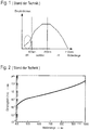
- UV-sensitive photodiodes based on silicon are known. However, it is disadvantageous for the use of Si diodes in the UV wavelength range that the sensitivity or sensitivity maximum lies in the wavelength range of (600 to 800) nm.
- the terms sensitivity and sensitivity are used synonymously.
- the sensitivity of the Si diodes is lower than in the VIS / IR wavelength range ( Fig.1 ).
- VIS describes the visible, ie the visual range of the electromagnetic spectrum and IR the infrared range.
- filters are used, which are transparent only for the UV wavelength range of interest and impermeable to any other radiation of the electromagnetic spectrum.
- Fig. 2 shows the penetration depth in silicon as a function of the wavelength of the incident radiation (http://www.elektroniknet.de/automation/sonstiges/izate/31 275/1 /).
- spectrally optimized UV photodiodes are known from the prior art.
- Spectrally optimized means that the spectral sensitivity maximum of the detectors in the UV range is (280 ... 400) nm, i. the detectors are optimized for measurements of UV content in an electromagnetic radiation spectrum. This can be influenced on the one hand by the choice of material for the photodiode used and thus by the predetermined spectral sensitivity characteristic, on the other hand, an additional filter can be used, which is transparent only for the UV wavelength range of interest.
- photodiodes based on silicon carbide, indium gallium nitride, gallium nitride or aluminum gallium nitride are known.
- UV photodiodes For example, at least one reference sensor is always necessary for a usable measurement. Also, no simple combination with other optical sensors, such as ambient light sensors (ALS), color or color temperature sensors (RGB sensor) or Proximity sensor (PS) is possible.
- ALS ambient light sensors
- RGB sensor color or color temperature sensors
- PS Proximity sensor
- the UV-sensitive photodiodes are also integrated in evaluation and control units comprehensive circuits, in so-called ICs.
- the disadvantage of known IC designs is that, in addition to low UV sensitivity, they also have a high spectral sensitivity in the visible and infrared ranges ( Fig.1 ) (see also DE 10 2012 001 481 A1 and DE 10 2012 001 070 A1 ).
- the UV component in a measured light spectrum can only be determined by means of correlation calculations, for which purpose the light spectrum must be known. In practice, however, this is often not the case.
- an optical sensor which, for example, on the spectrum of Sunlight normalized, erroneous readings when operating under artificial light supply, due to the different wavelength components in the spectrum of artificial and sunlight.
- a radiation source can be any body having a temperature above the absolute zero that emits electromagnetic radiation. Every body with a temperature above absolute zero emits a characteristic electromagnetic spectrum as a function of its temperature.
- the UV wavelength range of interest is (280 ... 400) nm.
- the range of (280 ... 320) nm is referred to as UV-B and the range of (320 ... 400) nm as UV-A, wherein the UV-A portion, which is dangerous for the human skin proportion.
- the IR wavelength range covers the wavelength range of (0, 78 ... 1000) ⁇ m.
- the VIS wavelength range covers the visible spectrum in the wavelength range of (400 ... 780) nm.
- a UV light sensor according to the preamble of claim 1, characterized in that the passivation layer is planar and the filter is formed directly on the planar passivation layer and stray light suppressing means around the at least one sensor element and / or to the UV Light sensor are formed.
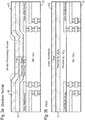
- a passivation layer of SiO 2 and Si 3 N 4 is applied to protect against mechanical damage and as a diffusion barrier for moisture and ions after the production of the last wiring level. It arises, as in Fig. 3a is shown, steps at the junctions between the sensitive sensor element and the contacting surface, so that no planar surface is realized.
- the SiO 2 passivation is leveled by a removal process, for example CMP and / or lapping, so that a planar deposition of the Si 3 N 4 passivation and the filter material over the entire chip area can be done ( Fig. 3b ).
- the life under harsh environmental conditions of the filter can be improved.
- the filter material can be deposited on a planar surface, whereby more uniform optical properties due to the homogeneous layer thicknesses of the filter or over the entire chip area can be achieved.
- both the vertical and the lateral / horizontal penetration of light on the sensor element or elements of the UV light sensor can be prevented.
- the stray light suppressing means are in one embodiment of the invention, at least partially by the Filter formed.
- the filter completely covers at least the respective sensor element, wherein the filter preferably still extends beyond the respective sensor element. It is particularly advantageous if the filter is formed over the entire surface of the entire UV light sensor, and even more advantageous if the filter extends over the entire IC, that is, up to its edge. The edge of the IC in which the UV light sensor is integrated is determined by the size of the Si substrate.
- the functional layer which is formed as at least one filter, can also be formed from different filter materials, wherein the filter edges overlap in such a way that the penetration of scattered light is prevented.
- the transition of the various filter materials is formed in the region of an active sensor surface, which is not a UV light sensor element. Although this reduces the optical opening of the underlying sensor element, it can achieve a significant reduction in scattered light coupling to adjacent UV light sensor elements of the matrix of sensor elements.
- the pads for contacting the UV light sensor with the subsequent electronics or the evaluation circuits are not covered by the functional layer.
- the scattered light-suppressing means are at least partially formed by a full-surface metal layer arranged on the UV light sensor and / or the entire IC and leaving the sensor elements free. This prevents penetration of light to the silicon surface at the locations that can not be covered by filters (eg, surfaces around the bond pads). Furthermore, low light, which due to a limited Stop band suppression of the filter would penetrate into the IC, shielded from hitting the silicon surface.
- the stray light suppressing means are at least partially formed by the UV light sensor laterally delimiting light barriers.
- Laterally delimiting light barriers are boundaries of suitable light-shielding materials which prevent lateral or lateral penetration of light into the UV light sensor and thus into the IC in which the UV light sensor is integrated.
- the stray light suppressing means are at least partially formed by an embedding of the UV light sensor in an opaque material, wherein the opaque material surrounds the edge of the UV light sensor.
- the opaque material may be a mold material which conforms to a material around the IC in a packaging process.
- the stray light suppressing means are at least partially formed by an opaque material on the back of the UV light sensor.
- the stray-light suppressing means are formed at least partially by trenches filled with opaque material, laterally delimiting the respective sensor element.
- the trenches can be formed by etching into the passivation layer so that so-called passivation etching trenches are formed. This can a suppression of light conduction in the passivation level can be effected.
- reflections and light conduction in intermetallic dielectrics in the metallization complex of the IC, i. the oxides between the wiring planes can be prevented by at least partially forming the light scattering suppressing means by light barriers perpendicular to the substrate surface in the CMOS wiring planes above the sensor elements formed in the substrate.
- the vertical light barriers in the CMOS wiring planes are formed by closed contact rings and / or staggered via rings up to a top metal plane of the CMOS process, whereby these only by the minimum necessary electrical contacting of the photodiodes, ie the sensor elements are interrupted.
- the penetration openings (vias) for the connection lines of the sensor elements are arranged offset, so that no continuous light path is formed.
- a light path describes the path from the point of penetration of the radiation into the substrate up to the sensitive sensor element.
- a plurality of sensor elements are arranged in a matrix, wherein the sensor elements comprise at least one photodiode with a UV filter, a photodiode as a trained ALS sensor and a photodiode with a poly-silicon cover and a UV filter. Include filters.
- the matrix can be formed as a 4x4 matrix with optimized half-space sensitivity, wherein the matrix is formed from four different sensor elements.
- the sensor elements can be used as a photodiode with UV filter and / or an ALS sensor and / or a photodiode with a Poly-silicon cover and a UV filter to be formed.
- the half-space of the UV light sensor includes the entire space above the UV light sensor, ie above the substrate level, wherein the sensitivity of the UV light sensor from each spatial direction of the half-space should be as equal as possible with an optimized half-space sensitivity.
- interference-based filters with high refractive index materials can be used for the various sensor elements to provide a low spectral To obtain angle dependence.
- the object of the invention is achieved by a method for detecting UV light with the proposed UV light sensor, wherein the one or more sensor elements detect light and deliver a signal in response to this, that a first output signal of a sensor element , which is designed as a photodiode, is measured that a second output signal of a sensor element, which is designed as a photodiode with a poly-silicon cover, measured and weighted by a factor, a mathematical relationship between the first and second output signal is determined.
- a mathematical link for example, the difference between the first and the second output signal can be calculated.
- the first output signal is formed by a UV component, a VIS / IR component and a leakage component
- the second output signal is formed by a weighted VIS / IR component and a weighted leakage component.
- the object of the invention is achieved in that a first output signal of a sensor element which is designed as a photodiode is measured, a second output signal of a sensor element which formed as a dark diode is measured and weighted by a factor, the dark diode is covered by an opaque metal and a mathematical link between the first and second output signal is detected.
- a mathematical link for example, the difference between the first and the second output signal can be calculated.
- the temperature-dependent dark currents (leakage currents) of the UV light sensor can be compensated by the dark diode due to the opaque metal cover only the leakage current is measured and thus the measurement signal of the photodiode can be corrected by these proportions.
- the two aforementioned compensation methods can also be combined, whereby both the VIS / IR sensitivity and the dark currents (leakage currents) can be compensated and thus a precise UV index value is determined.
- a monolithic integration of a single or multi-channel UV light sensor with evaluation units in a CMOS process can be carried out very easily.
- the spectral fit of the sensor sensitivities in the UV wavelength range can be adjusted by simply applying dedicated optical filters.
- By integrating into a CMOS process it is possible to combine the UV light sensor function with other environmental sensors, such as ALS, RGB, PS, pressure, gas, moisture, although this is not an exhaustive list.
- the inventive arrangement the penetration of stray light, which penetrates around the applied optical filter around in the UV light sensor or the IC can be prevented.
- Fig. 4 shows an embodiment of the invention, in which the filter 4 is formed over a large area on the IC 2 with the integrated UV light sensor 1 with associated signal processing 20. Thereby, a vertical penetration of light outside of one or more sensor elements 13 can be prevented. In this case, the pads for contacting 3 for the IC are not covered by the filter 4. It is also possible to arrange different filters 4, 5 via individual sensor elements 13, wherein different radiation components can then be detected with the sensor elements 13. In one embodiment, some sensor elements may be configured as dark diodes DD, to which no radiation is incident.
- Fig. 6 shows an embodiment of the invention, in which the stray light suppressing means of two different filter materials 4, 5 are formed.
- a UV filter 4 On the one hand from a UV filter 4 and on the other hand from a second filter material 5.
- the filters are arranged over a matrix of sensor elements 13, wherein the sensor elements 13 comprise UV and ALS sensor elements.
- the two filter materials 4, 5 are arranged such that the UV filter 4 is positioned over the UV sensor elements and the second filter material 5 over the ALS sensor elements. It is particularly advantageous if the expansion of the UV filter 4 extends into the optical opening 9 of the ALS sensor element ( Fig. 6b ). In this case, the aperture or aperture or optical opening of the ALS sensor element is reduced by the UV filter 4 and thus reduces its sensitivity, for example.
- 1/3 area corresponds to a decrease in the sensitivity of the ALS sensor element 13 by 1/3.
- the reduced sensitivity can be tolerated, as can be achieved by the overlap a significant reduction in the scattered light coupling to the adjacent UV sensor elements 13.
- significantly less stray light passes through the ALS filter 5 on the top metal.
- the coupled-in scattered light 7 would in turn be able to move toward the UV sensor elements 13 as in a light-light. This can be significantly reduced by the described embodiment.
- Fig. 7 shows a large-area metal cover 6 of the entire IC 2 with the integrated UV light sensor 1.
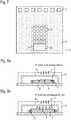
- Fig. 8 shows a schematic representation of an IC 2 with UV light sensor 1 in a housing 8. It shows Figure 8a the penetrating interference in the UV light sensor 1, due to the lack of stray light suppressing agent, whereas in Fig. 8b the IC 2 laterally limiting light barriers 10 are arranged to prevent the penetration of the interference in the UV light sensor 1 outside the sensitive sensor surface 1.
- Fig. 9 shows a kind of summary of possible stray-light suppressing agents.
- the vertical penetration of light 7 from the back of the IC 2 or UV light sensor 1 can be prevented by encapsulation with an opaque material 11, for example a suitable mold material in the packaging process.
- the horizontal penetration of light 7 over the IC chip edges can be achieved by covering the chip edge with suitable light-shielding materials 11 in the packaging process, for example, placing the IC 2 laterally delimiting light barriers 10, or the entire IC 2 in an opaque mold Material 11 is embedded.
- Fig. 10 shows a schematic representation of stray light suppressing means, which are formed of closed contact rings 12 and / or staggered via rings, whereby the penetration of scattered light by reflections or by light conduction in the intermetallic dielectrics in the metallization complex of the IC 2 (oxides between wiring levels) or passivation levels is prevented.
- Fig. 11 shows a schematic representation of the result of the compensation of the VIS / IR sensitivity of a Si photodiode by the compensation with a photodiode which is covered with poly-Si, for the case a) without UV filter and b) with UV filter, for which the method according to the invention for the detection of UV light with a UV light sensor 1 was used.
- the VIS / IR Sensitivity of the Si diodes can be suppressed by the following exemplary method steps:
- the output signal of the UV diode is measured. This is composed of the proportions UV + VIS / IR scattered light + leakage current.
- the poly-UV diode measures a second output signal. This consists of the proportions a1 * VIS / IR scattered light + a2 * leakage current.
- the scattered light of both diodes is not identical, represented by the factor a1, which is not equal to 1.
- the difference would not be exactly the desired UV component, so the compensation is not optimal.
- the optimization is achieved by forming a weighted difference, for example, the UV-poly diode is first weighted with 1 / (a1) and then the difference is formed. The leakage currents are compensated for when a2 is (nearly) 1.
- vertically stacked PN junctions Si pinched diodes
- Si pinched diodes can also be used to eliminate the VIS / IR sensitivity from the photocurrent used.
- a compensation method is also used for suppressing temperature-dependent and production-related leakage currents, wherein in a UV light sensor (1) comprising at least one photodiode with UV filter (UV diode) and at least one covered with a metal layer Dark diode (DD), the temperature-dependent and production-related leakage currents of the Si diodes can be suppressed by the following exemplary method steps: The output signal of the UV diode is measured. This is composed of the proportions UV + leakage current. The dark diode measures a second output signal. This includes the share a2 * leakage current. Subsequently, for example, a compensation by subtraction of the two measured output signals.
- DD metal layer Dark diode
- the optimization is achieved by forming a weighted difference, for example, first weighting the dark diode with 1 / (a2) and then forming the difference.
- a2 is not equal to 1
- the optimization is achieved by forming a weighted difference, for example, first weighting the dark diode with 1 / (a2) and then forming the difference.
- trim values for realizing a chip and diode-related programmable dark current calibration.
- UV light sensor 1 from at least one photodiode with UV filter (UV diode), at least one covered with a polysilicon layer photodiode with UV filter (UV poly-diode) and at least one covered with a metal layer dark diode DD At the same time, a compensation of the VIS / IR sensitivity and the leakage currents of the Si photodiodes can take place.
- the UV light sensor 1 a photodiode with UV filter (D1), a Photodiode with UV filter covered with a polysilicon layer (D2) and a metal-covered UV dark diode (D3)
- D 1 UV + VIS / IR - litter + Leakage current
- D 2 a 1 * VIS / IR - litter + a 2 _ 2 * Leakage current
- D3 + a 2 _ 3 * Leakage current.
- the homogenization of the leakage currents can also be done by optimized annealing in the manufacturing process.
- the UV light sensor 1 consists of a matrix of several sensor elements ( Fig. 12 ), can be homogenized by a composite according to certain arrangement criteria filter arrangement, wherein the filters consist of functionally dependent filter materials, remaining stray light - or different leakage current effects. For example, it is thus also possible to compensate for an optimal half-space sensitivity of the UV light sensor 1 and, under certain circumstances, a suppression of particles or production residues on the UV light sensor 1.
- the sensor elements 13 forming the UV light sensor 1 are arranged in a matrix structure, wherein an equal weighting message of light components from all spatial directions above the UV light sensor takes place by means of a geometric center of gravity.
- these 16 photodiodes four different filter materials associated with, ie the photodiodes fulfill different functions according to their associated filter, so the filter assignment meet the following criteria:
- the four different filters are arranged once in the corner, twice at the side edge, once per line, once per column, and once in the four 2x2 subquadars.
- the four different filters are then also assigned to different measuring channels.
- Fig. 12 shows such an arrangement of different filters. It is particularly advantageous that in the array incoming stray light, for example, when the designated G filter instead of with UV filter is covered with another filter, for example.
- a photo-optical filter visible light enters through this filter, which then to the UV diodes and UV poly-diodes can scatter. In order not to adversely affect their scattered light compensation, these diodes should see as much as possible scattered light components, even at different angles of incidence of the light.
Landscapes
- Physics & Mathematics (AREA)
- General Physics & Mathematics (AREA)
- Spectroscopy & Molecular Physics (AREA)
- Photometry And Measurement Of Optical Pulse Characteristics (AREA)
- Light Receiving Elements (AREA)
- Solid State Image Pick-Up Elements (AREA)
- Engineering & Computer Science (AREA)
- Microelectronics & Electronic Packaging (AREA)
- Measurement Of Radiation (AREA)
- Testing Or Measuring Of Semiconductors Or The Like (AREA)
Claims (21)
- Capteur de lumière UV (1), fabriqué avec un processus CMOS, comprenant un substrat ayant une surface, un ou plusieurs éléments capteurs (13) qui détectent un rayonnement et qui sont réalisés dans le substrat (15), au moins une couche de passivation (17) disposée au-dessus de la surface du substrat, ainsi qu'une couche fonctionnelle (18) disposée au-dessus de la couche de passivation (17), la couche fonctionnelle (18) étant réalisée sous la forme d'au moins un filtre (4, 5), la couche de passivation (17) est réalisée plane au moyen d'un processus d'enlèvement et le filtre (4, 5) est formé directement sur la couche de passivation (17) plane et des moyens de suppression de la lumière parasite sont réalisés autour de l'au moins un élément capteur (13) et/ou autour du capteur de lumière UV (1), caractérisé en ce que les moyens de suppression de la lumière parasite sont formés au moins partiellement par des barrières à lumière (10) verticales par rapport à la surface du substrat dans les plans de câblage CMOS au-dessus des éléments capteurs (13) réalisés dans le substrat (15).
- Capteur de lumière UV selon la revendication 1, caractérisé en ce que les moyens de suppression de la lumière parasite sont formés au moins partiellement par le filtre (4, 5).
- Capteur de lumière UV selon la revendication 1 ou 2, caractérisé en ce que les moyens de suppression de la lumière parasite sont formés au moins partiellement par une couche métallique disposée sur toute la surface du capteur de lumière UV (1) en laissant les éléments capteurs (13) dégagés.
- Capteur de lumière UV selon au moins l'une des revendications précédentes, caractérisé en ce que les moyens de suppression de la lumière parasite sont formés au moins partiellement par des barrières à lumière (10) qui délimitent latéralement le capteur de lumière UV (1).
- Capteur de lumière UV selon au moins l'une des revendications précédentes, caractérisé en ce que les moyens de suppression de la lumière parasite sont formés au moins partiellement par un enrobage du capteur de lumière UV (1) dans un matériau opaque (11), le matériau opaque (11) entourant le bord du capteur de lumière UV (1).
- Capteur de lumière UV selon au moins l'une des revendications précédentes, caractérisé en ce que les moyens de suppression de la lumière parasite sont formés au moins partiellement par un matériau opaque (11) sur le côté arrière du capteur de lumière UV (1).
- Capteur de lumière UV selon au moins l'une des revendications précédentes, caractérisé en ce que les moyens de suppression de la lumière parasite sont formés au moins partiellement par des tranchées remplies d'un matériau opaque (11) qui délimitent latéralement l'élément capteur (13) correspondant.
- Capteur de lumière UV selon la revendication 1, caractérisé en ce que les barrières à lumière (10) verticales dans les plans de câblage CMOS sont formées par des anneaux de contact (12) fermés et/ou des bagues d'interconnexion de configuration décalée jusque dans un plan métallique supérieur du processus CMOS.
- Capteur de lumière UV selon au moins l'une des revendications précédentes, caractérisé en ce que les éléments capteurs (13) qui détectent un rayonnement sont disposés en une matrice.
- Capteur de lumière UV selon au moins l'une des revendications précédentes, caractérisé en ce que des filtres (4, 5) en différents matériaux filtrants sont réalisés au-dessus des éléments capteurs (13) qui détectent un rayonnement, les filtres (4, 5) se chevauchant partiellement e/ou les deux filtres (4, 5) étant réalisés pour recouvrir partiellement la surface d'élément capteur (14) active.
- Capteur de lumière UV selon au moins l'une des revendications précédentes, caractérisé en ce que les éléments capteurs (13) sont réalisés sous la forme de photodiodes et/ou de capteurs ALS et/ou de capteurs à compensation du courant d'obscurité.
- Capteur de lumière UV selon au moins l'une des revendications 1 à 11, caractérisé en ce que plusieurs éléments capteurs (13) sont disposés en une matrice, les éléments capteurs (13) comprenant au moins une photodiode dotée d'un filtre à UV, un capteur ALS et une photodiode dotée d'un cache en polysilicium et d'un filtre à UV (4).
- Capteur de lumière UV selon la revendication 12, caractérisé en ce que la matrice est réalisée sous la forme d'une matrice 4x4 avec sensibilité en demi-espace optimisée, composée de quatre éléments capteurs (13) différents.
- Capteur de lumière UV selon la revendication 13, caractérisé en ce que la sensibilité en demi-espace optimisée est réglée par le fait que différents éléments capteurs (13) répondent aux critères d'arrangement suivants :- chaque élément capteur est disposé une fois dans le coin de la matrice de diodes,- chaque élément capteur est disposé deux fois au niveau de l'arête latérale de la matrice de diodes,- chaque élément capteur est disposé une fois par ligne de la matrice de diodes,- chaque élément capteur est disposé une fois par colonne de la matrice de diodes,- chaque élément capteur est disposé une fois dans les 4 sous-carrés de 2x2 de la matrice de diodes.
- Procédé de détection de lumière UV avec un capteur de lumière UV selon au moins l'une des revendications précédentes, l'un ou les plusieurs éléments détecteurs (13) détectant de la lumière et délivrant un signal en réaction à celle-ci, caractérisé en ce que- un premier signal de sortie d'un élément capteur, lequel est réalisé sous la forme d'une photodiode, est mesuré, en ce que- un deuxième signal de sortie d'un élément capteur, lequel est réalisé sous la forme d'une photodiode avec un cache en polysilicium, est mesuré puis pondéré avec un facteur,- une liaison mathématique entre le premier et le deuxième signal de sortie est déterminée.
- Procédé selon la revendication 15, caractérisé en ce que la liaison mathématique calculée est la différence entre le premier et le deuxième signal de sortie.
- Procédé selon la revendication 16, caractérisé en ce que le premier signal de sortie est formé par une part UV, une part VIS/IR et une part de courant de fuite.
- Procédé selon la revendication 16, caractérisé en ce que le deuxième signal de sortie est formé par une part VIS/IR pondérée et une part de courant de fuite pondérée.
- Procédé de détection de lumière UV avec un capteur de lumière UV selon au moins l'une des revendications 1 à 13, l'un ou les plusieurs éléments détecteurs détectant de la lumière et délivrant un signal en réaction à celle-ci, caractérisé en ce que- un premier signal de sortie d'un élément capteur, lequel est réalisé sous la forme d'une photodiode, est mesuré, en ce que- un deuxième signal de sortie d'un élément capteur, lequel est réalisé sous la forme d'une diode d'obscurité, la diode d'obscurité étant recouverte d'un métal opaque, est mesuré puis pondéré avec un facteur,- une liaison mathématique entre le premier et le deuxième signal de sortie est déterminée.
- Procédé selon la revendication 19, caractérisé en ce que la liaison mathématique calculée est la différence entre le premier et le deuxième signal de sortie.
- Procédé selon la revendication 19, caractérisé par les caractéristiques d'au moins l'une des revendications 15 à 18.
Applications Claiming Priority (2)
| Application Number | Priority Date | Filing Date | Title |
|---|---|---|---|
| DE102014107062 | 2014-05-19 | ||
| PCT/EP2015/060969 WO2015177129A1 (fr) | 2014-05-19 | 2015-05-19 | Capteur de lumière uv à suppression de lumière diffusée et procédé de détection de lumière uv |
Publications (2)
| Publication Number | Publication Date |
|---|---|
| EP3146568A1 EP3146568A1 (fr) | 2017-03-29 |
| EP3146568B1 true EP3146568B1 (fr) | 2018-07-11 |
Family
ID=52814057
Family Applications (1)
| Application Number | Title | Priority Date | Filing Date |
|---|---|---|---|
| EP15724976.4A Active EP3146568B1 (fr) | 2014-05-19 | 2015-05-19 | Capteur de lumière uv à suppression de lumière diffusée et procédé de détection de lumière uv |
Country Status (7)
| Country | Link |
|---|---|
| US (1) | US10041829B2 (fr) |
| EP (1) | EP3146568B1 (fr) |
| KR (1) | KR102315874B1 (fr) |
| CN (1) | CN106605130B (fr) |
| DE (2) | DE102014111945A1 (fr) |
| TW (3) | TWI578397B (fr) |
| WO (3) | WO2015176834A1 (fr) |
Families Citing this family (7)
| Publication number | Priority date | Publication date | Assignee | Title |
|---|---|---|---|---|
| CN105047674B (zh) * | 2015-08-06 | 2018-09-04 | 京东方科技集团股份有限公司 | 阵列基板及其制备方法和显示装置 |
| CN109946778A (zh) * | 2017-12-21 | 2019-06-28 | 张家港康得新光电材料有限公司 | 光学膜片及具有其的环境光传感器 |
| EP3537118B1 (fr) * | 2018-03-08 | 2024-04-03 | MEAS France | Capteur de rayonnement, agencement de capteur de véhicule et procédé d'assemblage |
| DE102018130510A1 (de) * | 2018-11-30 | 2020-06-04 | Vishay Semiconductor Gmbh | Strahlungssensor und Herstellungsverfahren hierfür |
| US11373967B2 (en) * | 2019-11-14 | 2022-06-28 | Advanced Semiconductor Engineering, Inc. | Semiconductor device package and method for packaging the same |
| CN215867092U (zh) * | 2019-11-29 | 2022-02-18 | 深圳市大疆创新科技有限公司 | 光探测器、探测模组和探测装置 |
| KR102624144B1 (ko) * | 2023-09-21 | 2024-01-12 | 대성제관공업주식회사 | 알콜캔 캡 자동 분리공급장치 |
Family Cites Families (22)
| Publication number | Priority date | Publication date | Assignee | Title |
|---|---|---|---|---|
| US6821810B1 (en) | 2000-08-07 | 2004-11-23 | Taiwan Semiconductor Manufacturing Company | High transmittance overcoat for optimization of long focal length microlens arrays in semiconductor color imagers |
| US6911392B2 (en) * | 2001-08-24 | 2005-06-28 | Schott Glas | Process for making contact with and housing integrated circuits |
| DE10258509B4 (de) * | 2002-12-14 | 2005-10-20 | Infineon Technologies Ag | Verfahren zur Herstellung eines dünnen bruchfesten Halbleiterwafers |
| JP2004319530A (ja) * | 2003-02-28 | 2004-11-11 | Sanyo Electric Co Ltd | 光半導体装置およびその製造方法 |
| US20040200975A1 (en) * | 2003-04-14 | 2004-10-14 | Brown Dale Marius | Ultraviolet sensors for monitoring energy in the germicidal wavelengths |
| WO2005024404A1 (fr) * | 2003-09-04 | 2005-03-17 | Kla-Tencor Technologies | Procedes et systemes permettant d'inspecter un specimen a l'aide de differents parametres d'inspection |
| US7294827B2 (en) | 2004-09-21 | 2007-11-13 | Delphi Technologies, Inc. | Electronic module with light-blocking features |
| JP4761505B2 (ja) | 2005-03-01 | 2011-08-31 | キヤノン株式会社 | 撮像装置、ならびに撮像システム |
| CN100472791C (zh) * | 2005-06-17 | 2009-03-25 | 凸版印刷株式会社 | 摄像元件 |
| KR100866718B1 (ko) * | 2005-06-17 | 2008-11-05 | 도판 인사츠 가부시키가이샤 | 촬상 소자 |
| JP4832273B2 (ja) * | 2006-12-13 | 2011-12-07 | 日立マクセル株式会社 | 生体認証用撮像モジュール、生体認証装置及びプリズム |
| GB2446821A (en) * | 2007-02-07 | 2008-08-27 | Sharp Kk | An ambient light sensing system |
| US7727875B2 (en) * | 2007-06-21 | 2010-06-01 | Stats Chippac, Ltd. | Grooving bumped wafer pre-underfill system |
| US8885987B2 (en) * | 2007-09-06 | 2014-11-11 | Quantum Semiconductor Llc | Photonic via waveguide for pixel arrays |
| JP5344336B2 (ja) * | 2008-02-27 | 2013-11-20 | 株式会社ザイキューブ | 半導体装置 |
| CN101661943B (zh) * | 2008-08-26 | 2011-01-26 | 北京大学 | 一种单片集成紫外图像传感器及其像素单元以及制备方法 |
| CN101393922B (zh) * | 2008-10-30 | 2011-06-15 | 旭丽电子(广州)有限公司 | 镜头模组及其制作方法 |
| JP5498684B2 (ja) * | 2008-11-07 | 2014-05-21 | ラピスセミコンダクタ株式会社 | 半導体モジュール及びその製造方法 |
| JP2010271049A (ja) * | 2009-05-19 | 2010-12-02 | Sony Corp | 2次元固体撮像装置 |
| US8598672B2 (en) | 2011-01-26 | 2013-12-03 | Maxim Integrated Products, Inc | Light sensor having IR cut interference filter with color filter integrated on-chip |
| US8803068B2 (en) | 2011-01-26 | 2014-08-12 | Maxim Integrated Products, Inc. | Light sensor having a contiguous IR suppression filter and a transparent substrate |
| TWI528533B (zh) * | 2012-07-06 | 2016-04-01 | 恆景科技股份有限公司 | 光偵測器及其製造方法 |
-
2014
- 2014-08-21 DE DE102014111945.2A patent/DE102014111945A1/de not_active Ceased
-
2015
- 2015-03-04 TW TW104106879A patent/TWI578397B/zh not_active IP Right Cessation
- 2015-03-04 WO PCT/EP2015/054506 patent/WO2015176834A1/fr not_active Ceased
- 2015-03-04 DE DE112015002389.5T patent/DE112015002389B4/de active Active
- 2015-05-19 TW TW104115831A patent/TWI580935B/zh active
- 2015-05-19 US US15/312,522 patent/US10041829B2/en active Active
- 2015-05-19 KR KR1020167035392A patent/KR102315874B1/ko active Active
- 2015-05-19 WO PCT/EP2015/060954 patent/WO2015177115A1/fr not_active Ceased
- 2015-05-19 EP EP15724976.4A patent/EP3146568B1/fr active Active
- 2015-05-19 CN CN201580039107.XA patent/CN106605130B/zh active Active
- 2015-05-19 TW TW104115830A patent/TW201600834A/zh unknown
- 2015-05-19 WO PCT/EP2015/060969 patent/WO2015177129A1/fr not_active Ceased
Non-Patent Citations (1)
| Title |
|---|
| None * |
Also Published As
| Publication number | Publication date |
|---|---|
| DE112015002389A5 (de) | 2017-02-09 |
| DE112015002389B4 (de) | 2024-01-11 |
| US10041829B2 (en) | 2018-08-07 |
| KR20170009926A (ko) | 2017-01-25 |
| WO2015177115A1 (fr) | 2015-11-26 |
| CN106605130B (zh) | 2019-06-28 |
| EP3146568A1 (fr) | 2017-03-29 |
| TWI580935B (zh) | 2017-05-01 |
| TW201600834A (zh) | 2016-01-01 |
| WO2015176834A1 (fr) | 2015-11-26 |
| TW201545236A (zh) | 2015-12-01 |
| WO2015177129A1 (fr) | 2015-11-26 |
| DE102014111945A1 (de) | 2015-11-19 |
| US20170108372A1 (en) | 2017-04-20 |
| KR102315874B1 (ko) | 2021-10-20 |
| TWI578397B (zh) | 2017-04-11 |
| TW201544800A (zh) | 2015-12-01 |
| CN106605130A (zh) | 2017-04-26 |
Similar Documents
| Publication | Publication Date | Title |
|---|---|---|
| EP3146568A1 (fr) | Capteur de lumière uv à suppression de lumière diffusée et procédé de détection de lumière uv | |
| AT507702B1 (de) | Detektorfläche | |
| DE69935550T2 (de) | Photodetektor und Strahlungsdetektionssystem | |
| EP2210073B1 (fr) | Circuiterie pour la production de signaux dépendant de la luminosité et de la température, notamment pour un pyromètre produisant des images | |
| CH684971A5 (de) | Ultraviolettlicht-Sensor. | |
| DE102008016167A1 (de) | Farbsensor mit Infrarotkorrektur | |
| DE112013004275T5 (de) | Gewundener IR-Sensor | |
| DE112021000990T5 (de) | Verbesserungen für spad-basierte fotodetektoren | |
| DE112018006397T5 (de) | Silizium-drift-detektionselement, silizium-drift-detektor und strahlungsdetektionsvorrichtung | |
| WO2021028175A1 (fr) | Procédé et dispositif d'analyse d'une cellule solaire multijonction dotée d'au moins deux sous-cellules solaires au moyen d'un rayonnement luminescent | |
| US9683889B2 (en) | Ultraviolet semiconductor sensor device and method of measuring ultraviolet radiation | |
| EP2902757A1 (fr) | Capteur optique et procédé et dispositif de fabrication d'un capteur optique | |
| DE112021004422T5 (de) | Erfassung von umgebungsstrahlung | |
| DE10239643B3 (de) | Verfahren zur Passivierung von CMOS- oder BiCMOS-IC's mit integrierten fotoempfindlichen Strukturen | |
| DE102010047061A1 (de) | Optisches Weitbereichsspektrometer | |
| DE102006002732A1 (de) | Photomischdetektor und Verfahren zu dessen Betrieb | |
| EP0935819A1 (fr) | Capteurs tfa hybrides a composants a circuit integre specifique sensibles au rayonnement | |
| DE10334818A1 (de) | Röntgendetektor | |
| WO1995024738A1 (fr) | Detecteur semi-conducteur de rayonnements a ondes courtes et son procede de fabrication | |
| DE102016111253A1 (de) | Vorrichtung mit einem Infrarotdetektor und einem vorgelagerten Schutzfenster | |
| WO1995005586A1 (fr) | Procede et appareil de mesure du rayonnement d'un domaine spectral | |
| DE10101457A1 (de) | Optoelektronisches System zur Detektion elektromagnetischer Strahlung | |
| WO2010094374A1 (fr) | Photodétecteur et matrice de photodétecteurs | |
| WO2003083952A2 (fr) | Dispositif et capteur servant a enregistrer des signaux lumineux et procede de production | |
| WO2013156013A1 (fr) | Dispositif de detection optique |
Legal Events
| Date | Code | Title | Description |
|---|---|---|---|
| STAA | Information on the status of an ep patent application or granted ep patent |
Free format text: STATUS: THE INTERNATIONAL PUBLICATION HAS BEEN MADE |
|
| PUAI | Public reference made under article 153(3) epc to a published international application that has entered the european phase |
Free format text: ORIGINAL CODE: 0009012 |
|
| STAA | Information on the status of an ep patent application or granted ep patent |
Free format text: STATUS: REQUEST FOR EXAMINATION WAS MADE |
|
| 17P | Request for examination filed |
Effective date: 20161205 |
|
| AK | Designated contracting states |
Kind code of ref document: A1 Designated state(s): AL AT BE BG CH CY CZ DE DK EE ES FI FR GB GR HR HU IE IS IT LI LT LU LV MC MK MT NL NO PL PT RO RS SE SI SK SM TR |
|
| AX | Request for extension of the european patent |
Extension state: BA ME |
|
| DAV | Request for validation of the european patent (deleted) | ||
| DAX | Request for extension of the european patent (deleted) | ||
| GRAP | Despatch of communication of intention to grant a patent |
Free format text: ORIGINAL CODE: EPIDOSNIGR1 |
|
| STAA | Information on the status of an ep patent application or granted ep patent |
Free format text: STATUS: GRANT OF PATENT IS INTENDED |
|
| INTG | Intention to grant announced |
Effective date: 20180131 |
|
| GRAJ | Information related to disapproval of communication of intention to grant by the applicant or resumption of examination proceedings by the epo deleted |
Free format text: ORIGINAL CODE: EPIDOSDIGR1 |
|
| STAA | Information on the status of an ep patent application or granted ep patent |
Free format text: STATUS: REQUEST FOR EXAMINATION WAS MADE |
|
| GRAR | Information related to intention to grant a patent recorded |
Free format text: ORIGINAL CODE: EPIDOSNIGR71 |
|
| GRAS | Grant fee paid |
Free format text: ORIGINAL CODE: EPIDOSNIGR3 |
|
| STAA | Information on the status of an ep patent application or granted ep patent |
Free format text: STATUS: GRANT OF PATENT IS INTENDED |
|
| GRAA | (expected) grant |
Free format text: ORIGINAL CODE: 0009210 |
|
| STAA | Information on the status of an ep patent application or granted ep patent |
Free format text: STATUS: THE PATENT HAS BEEN GRANTED |
|
| INTC | Intention to grant announced (deleted) | ||
| INTG | Intention to grant announced |
Effective date: 20180530 |
|
| AK | Designated contracting states |
Kind code of ref document: B1 Designated state(s): AL AT BE BG CH CY CZ DE DK EE ES FI FR GB GR HR HU IE IS IT LI LT LU LV MC MK MT NL NO PL PT RO RS SE SI SK SM TR |
|
| REG | Reference to a national code |
Ref country code: GB Ref legal event code: FG4D Free format text: NOT ENGLISH |
|
| REG | Reference to a national code |
Ref country code: CH Ref legal event code: EP |
|
| REG | Reference to a national code |
Ref country code: AT Ref legal event code: REF Ref document number: 1017801 Country of ref document: AT Kind code of ref document: T Effective date: 20180715 |
|
| REG | Reference to a national code |
Ref country code: IE Ref legal event code: FG4D Free format text: LANGUAGE OF EP DOCUMENT: GERMAN |
|
| REG | Reference to a national code |
Ref country code: DE Ref legal event code: R096 Ref document number: 502015005033 Country of ref document: DE |
|
| REG | Reference to a national code |
Ref country code: NL Ref legal event code: MP Effective date: 20180711 |
|
| REG | Reference to a national code |
Ref country code: LT Ref legal event code: MG4D |
|
| PG25 | Lapsed in a contracting state [announced via postgrant information from national office to epo] |
Ref country code: NL Free format text: LAPSE BECAUSE OF FAILURE TO SUBMIT A TRANSLATION OF THE DESCRIPTION OR TO PAY THE FEE WITHIN THE PRESCRIBED TIME-LIMIT Effective date: 20180711 |
|
| PG25 | Lapsed in a contracting state [announced via postgrant information from national office to epo] |
Ref country code: FI Free format text: LAPSE BECAUSE OF FAILURE TO SUBMIT A TRANSLATION OF THE DESCRIPTION OR TO PAY THE FEE WITHIN THE PRESCRIBED TIME-LIMIT Effective date: 20180711 Ref country code: SE Free format text: LAPSE BECAUSE OF FAILURE TO SUBMIT A TRANSLATION OF THE DESCRIPTION OR TO PAY THE FEE WITHIN THE PRESCRIBED TIME-LIMIT Effective date: 20180711 Ref country code: BG Free format text: LAPSE BECAUSE OF FAILURE TO SUBMIT A TRANSLATION OF THE DESCRIPTION OR TO PAY THE FEE WITHIN THE PRESCRIBED TIME-LIMIT Effective date: 20181011 Ref country code: GR Free format text: LAPSE BECAUSE OF FAILURE TO SUBMIT A TRANSLATION OF THE DESCRIPTION OR TO PAY THE FEE WITHIN THE PRESCRIBED TIME-LIMIT Effective date: 20181012 Ref country code: RS Free format text: LAPSE BECAUSE OF FAILURE TO SUBMIT A TRANSLATION OF THE DESCRIPTION OR TO PAY THE FEE WITHIN THE PRESCRIBED TIME-LIMIT Effective date: 20180711 Ref country code: NO Free format text: LAPSE BECAUSE OF FAILURE TO SUBMIT A TRANSLATION OF THE DESCRIPTION OR TO PAY THE FEE WITHIN THE PRESCRIBED TIME-LIMIT Effective date: 20181011 Ref country code: PL Free format text: LAPSE BECAUSE OF FAILURE TO SUBMIT A TRANSLATION OF THE DESCRIPTION OR TO PAY THE FEE WITHIN THE PRESCRIBED TIME-LIMIT Effective date: 20180711 Ref country code: IS Free format text: LAPSE BECAUSE OF FAILURE TO SUBMIT A TRANSLATION OF THE DESCRIPTION OR TO PAY THE FEE WITHIN THE PRESCRIBED TIME-LIMIT Effective date: 20181111 Ref country code: LT Free format text: LAPSE BECAUSE OF FAILURE TO SUBMIT A TRANSLATION OF THE DESCRIPTION OR TO PAY THE FEE WITHIN THE PRESCRIBED TIME-LIMIT Effective date: 20180711 |
|
| PG25 | Lapsed in a contracting state [announced via postgrant information from national office to epo] |
Ref country code: AL Free format text: LAPSE BECAUSE OF FAILURE TO SUBMIT A TRANSLATION OF THE DESCRIPTION OR TO PAY THE FEE WITHIN THE PRESCRIBED TIME-LIMIT Effective date: 20180711 Ref country code: HR Free format text: LAPSE BECAUSE OF FAILURE TO SUBMIT A TRANSLATION OF THE DESCRIPTION OR TO PAY THE FEE WITHIN THE PRESCRIBED TIME-LIMIT Effective date: 20180711 Ref country code: LV Free format text: LAPSE BECAUSE OF FAILURE TO SUBMIT A TRANSLATION OF THE DESCRIPTION OR TO PAY THE FEE WITHIN THE PRESCRIBED TIME-LIMIT Effective date: 20180711 |
|
| REG | Reference to a national code |
Ref country code: DE Ref legal event code: R097 Ref document number: 502015005033 Country of ref document: DE |
|
| PG25 | Lapsed in a contracting state [announced via postgrant information from national office to epo] |
Ref country code: ES Free format text: LAPSE BECAUSE OF FAILURE TO SUBMIT A TRANSLATION OF THE DESCRIPTION OR TO PAY THE FEE WITHIN THE PRESCRIBED TIME-LIMIT Effective date: 20180711 Ref country code: CZ Free format text: LAPSE BECAUSE OF FAILURE TO SUBMIT A TRANSLATION OF THE DESCRIPTION OR TO PAY THE FEE WITHIN THE PRESCRIBED TIME-LIMIT Effective date: 20180711 Ref country code: RO Free format text: LAPSE BECAUSE OF FAILURE TO SUBMIT A TRANSLATION OF THE DESCRIPTION OR TO PAY THE FEE WITHIN THE PRESCRIBED TIME-LIMIT Effective date: 20180711 Ref country code: IT Free format text: LAPSE BECAUSE OF FAILURE TO SUBMIT A TRANSLATION OF THE DESCRIPTION OR TO PAY THE FEE WITHIN THE PRESCRIBED TIME-LIMIT Effective date: 20180711 Ref country code: EE Free format text: LAPSE BECAUSE OF FAILURE TO SUBMIT A TRANSLATION OF THE DESCRIPTION OR TO PAY THE FEE WITHIN THE PRESCRIBED TIME-LIMIT Effective date: 20180711 |
|
| PLBE | No opposition filed within time limit |
Free format text: ORIGINAL CODE: 0009261 |
|
| STAA | Information on the status of an ep patent application or granted ep patent |
Free format text: STATUS: NO OPPOSITION FILED WITHIN TIME LIMIT |
|
| PG25 | Lapsed in a contracting state [announced via postgrant information from national office to epo] |
Ref country code: DK Free format text: LAPSE BECAUSE OF FAILURE TO SUBMIT A TRANSLATION OF THE DESCRIPTION OR TO PAY THE FEE WITHIN THE PRESCRIBED TIME-LIMIT Effective date: 20180711 Ref country code: SM Free format text: LAPSE BECAUSE OF FAILURE TO SUBMIT A TRANSLATION OF THE DESCRIPTION OR TO PAY THE FEE WITHIN THE PRESCRIBED TIME-LIMIT Effective date: 20180711 Ref country code: SK Free format text: LAPSE BECAUSE OF FAILURE TO SUBMIT A TRANSLATION OF THE DESCRIPTION OR TO PAY THE FEE WITHIN THE PRESCRIBED TIME-LIMIT Effective date: 20180711 |
|
| 26N | No opposition filed |
Effective date: 20190412 |
|
| PG25 | Lapsed in a contracting state [announced via postgrant information from national office to epo] |
Ref country code: SI Free format text: LAPSE BECAUSE OF FAILURE TO SUBMIT A TRANSLATION OF THE DESCRIPTION OR TO PAY THE FEE WITHIN THE PRESCRIBED TIME-LIMIT Effective date: 20180711 |
|
| REG | Reference to a national code |
Ref country code: CH Ref legal event code: PL |
|
| GBPC | Gb: european patent ceased through non-payment of renewal fee |
Effective date: 20190519 |
|
| PG25 | Lapsed in a contracting state [announced via postgrant information from national office to epo] |
Ref country code: LI Free format text: LAPSE BECAUSE OF NON-PAYMENT OF DUE FEES Effective date: 20190531 Ref country code: CH Free format text: LAPSE BECAUSE OF NON-PAYMENT OF DUE FEES Effective date: 20190531 Ref country code: MC Free format text: LAPSE BECAUSE OF FAILURE TO SUBMIT A TRANSLATION OF THE DESCRIPTION OR TO PAY THE FEE WITHIN THE PRESCRIBED TIME-LIMIT Effective date: 20180711 |
|
| REG | Reference to a national code |
Ref country code: BE Ref legal event code: MM Effective date: 20190531 |
|
| PG25 | Lapsed in a contracting state [announced via postgrant information from national office to epo] |
Ref country code: LU Free format text: LAPSE BECAUSE OF NON-PAYMENT OF DUE FEES Effective date: 20190519 |
|
| PG25 | Lapsed in a contracting state [announced via postgrant information from national office to epo] |
Ref country code: TR Free format text: LAPSE BECAUSE OF FAILURE TO SUBMIT A TRANSLATION OF THE DESCRIPTION OR TO PAY THE FEE WITHIN THE PRESCRIBED TIME-LIMIT Effective date: 20180711 |
|
| PG25 | Lapsed in a contracting state [announced via postgrant information from national office to epo] |
Ref country code: GB Free format text: LAPSE BECAUSE OF NON-PAYMENT OF DUE FEES Effective date: 20190519 Ref country code: IE Free format text: LAPSE BECAUSE OF NON-PAYMENT OF DUE FEES Effective date: 20190519 |
|
| PG25 | Lapsed in a contracting state [announced via postgrant information from national office to epo] |
Ref country code: BE Free format text: LAPSE BECAUSE OF NON-PAYMENT OF DUE FEES Effective date: 20190531 |
|
| PG25 | Lapsed in a contracting state [announced via postgrant information from national office to epo] |
Ref country code: PT Free format text: LAPSE BECAUSE OF FAILURE TO SUBMIT A TRANSLATION OF THE DESCRIPTION OR TO PAY THE FEE WITHIN THE PRESCRIBED TIME-LIMIT Effective date: 20181111 |
|
| PG25 | Lapsed in a contracting state [announced via postgrant information from national office to epo] |
Ref country code: CY Free format text: LAPSE BECAUSE OF FAILURE TO SUBMIT A TRANSLATION OF THE DESCRIPTION OR TO PAY THE FEE WITHIN THE PRESCRIBED TIME-LIMIT Effective date: 20180711 |
|
| REG | Reference to a national code |
Ref country code: AT Ref legal event code: MM01 Ref document number: 1017801 Country of ref document: AT Kind code of ref document: T Effective date: 20200519 |
|
| PG25 | Lapsed in a contracting state [announced via postgrant information from national office to epo] |
Ref country code: MT Free format text: LAPSE BECAUSE OF FAILURE TO SUBMIT A TRANSLATION OF THE DESCRIPTION OR TO PAY THE FEE WITHIN THE PRESCRIBED TIME-LIMIT Effective date: 20180711 Ref country code: HU Free format text: LAPSE BECAUSE OF FAILURE TO SUBMIT A TRANSLATION OF THE DESCRIPTION OR TO PAY THE FEE WITHIN THE PRESCRIBED TIME-LIMIT; INVALID AB INITIO Effective date: 20150519 |
|
| PG25 | Lapsed in a contracting state [announced via postgrant information from national office to epo] |
Ref country code: AT Free format text: LAPSE BECAUSE OF NON-PAYMENT OF DUE FEES Effective date: 20200519 |
|
| PG25 | Lapsed in a contracting state [announced via postgrant information from national office to epo] |
Ref country code: MK Free format text: LAPSE BECAUSE OF FAILURE TO SUBMIT A TRANSLATION OF THE DESCRIPTION OR TO PAY THE FEE WITHIN THE PRESCRIBED TIME-LIMIT Effective date: 20180711 |
|
| P01 | Opt-out of the competence of the unified patent court (upc) registered |
Effective date: 20230608 |
|
| REG | Reference to a national code |
Ref country code: DE Ref legal event code: R079 Ref document number: 502015005033 Country of ref document: DE Free format text: PREVIOUS MAIN CLASS: H01L0027144000 Ipc: H10F0039100000 |
|
| PGFP | Annual fee paid to national office [announced via postgrant information from national office to epo] |
Ref country code: DE Payment date: 20250528 Year of fee payment: 11 |
|
| PGFP | Annual fee paid to national office [announced via postgrant information from national office to epo] |
Ref country code: FR Payment date: 20250526 Year of fee payment: 11 |