EP3147830B1 - Schutz fuer eine integrierte schaltung - Google Patents
Schutz fuer eine integrierte schaltung Download PDFInfo
- Publication number
- EP3147830B1 EP3147830B1 EP15290240.9A EP15290240A EP3147830B1 EP 3147830 B1 EP3147830 B1 EP 3147830B1 EP 15290240 A EP15290240 A EP 15290240A EP 3147830 B1 EP3147830 B1 EP 3147830B1
- Authority
- EP
- European Patent Office
- Prior art keywords
- security
- critical component
- value
- active shield
- integrated circuit
- Prior art date
- Legal status (The legal status is an assumption and is not a legal conclusion. Google has not performed a legal analysis and makes no representation as to the accuracy of the status listed.)
- Active
Links
Images

Classifications
-
- G—PHYSICS
- G06—COMPUTING OR CALCULATING; COUNTING
- G06K—GRAPHICAL DATA READING; PRESENTATION OF DATA; RECORD CARRIERS; HANDLING RECORD CARRIERS
- G06K19/00—Record carriers for use with machines and with at least a part designed to carry digital markings
- G06K19/06—Record carriers for use with machines and with at least a part designed to carry digital markings characterised by the kind of the digital marking, e.g. shape, nature, code
- G06K19/067—Record carriers with conductive marks, printed circuits or semiconductor circuit elements, e.g. credit or identity cards also with resonating or responding marks without active components
- G06K19/07—Record carriers with conductive marks, printed circuits or semiconductor circuit elements, e.g. credit or identity cards also with resonating or responding marks without active components with integrated circuit chips
- G06K19/073—Special arrangements for circuits, e.g. for protecting identification code in memory
- G06K19/07309—Means for preventing undesired reading or writing from or onto record carriers
-
- G—PHYSICS
- G06—COMPUTING OR CALCULATING; COUNTING
- G06F—ELECTRIC DIGITAL DATA PROCESSING
- G06F21/00—Security arrangements for protecting computers, components thereof, programs or data against unauthorised activity
- G06F21/70—Protecting specific internal or peripheral components, in which the protection of a component leads to protection of the entire computer
- G06F21/86—Secure or tamper-resistant housings
- G06F21/87—Secure or tamper-resistant housings by means of encapsulation, e.g. for integrated circuits
-
- G—PHYSICS
- G06—COMPUTING OR CALCULATING; COUNTING
- G06F—ELECTRIC DIGITAL DATA PROCESSING
- G06F12/00—Accessing, addressing or allocating within memory systems or architectures
- G06F12/14—Protection against unauthorised use of memory or access to memory
- G06F12/1458—Protection against unauthorised use of memory or access to memory by checking the subject access rights
- G06F12/1466—Key-lock mechanism
-
- G—PHYSICS
- G06—COMPUTING OR CALCULATING; COUNTING
- G06F—ELECTRIC DIGITAL DATA PROCESSING
- G06F21/00—Security arrangements for protecting computers, components thereof, programs or data against unauthorised activity
- G06F21/30—Authentication, i.e. establishing the identity or authorisation of security principals
- G06F21/31—User authentication
- G06F21/316—User authentication by observing the pattern of computer usage, e.g. typical user behaviour
-
- G—PHYSICS
- G06—COMPUTING OR CALCULATING; COUNTING
- G06F—ELECTRIC DIGITAL DATA PROCESSING
- G06F12/00—Accessing, addressing or allocating within memory systems or architectures
- G06F12/14—Protection against unauthorised use of memory or access to memory
- G06F12/1408—Protection against unauthorised use of memory or access to memory by using cryptography
-
- G—PHYSICS
- G06—COMPUTING OR CALCULATING; COUNTING
- G06F—ELECTRIC DIGITAL DATA PROCESSING
- G06F21/00—Security arrangements for protecting computers, components thereof, programs or data against unauthorised activity
- G06F21/60—Protecting data
- G06F21/602—Providing cryptographic facilities or services
-
- G—PHYSICS
- G06—COMPUTING OR CALCULATING; COUNTING
- G06F—ELECTRIC DIGITAL DATA PROCESSING
- G06F21/00—Security arrangements for protecting computers, components thereof, programs or data against unauthorised activity
- G06F21/60—Protecting data
- G06F21/62—Protecting access to data via a platform, e.g. using keys or access control rules
-
- G—PHYSICS
- G06—COMPUTING OR CALCULATING; COUNTING
- G06F—ELECTRIC DIGITAL DATA PROCESSING
- G06F21/00—Security arrangements for protecting computers, components thereof, programs or data against unauthorised activity
- G06F21/70—Protecting specific internal or peripheral components, in which the protection of a component leads to protection of the entire computer
- G06F21/86—Secure or tamper-resistant housings
-
- G—PHYSICS
- G06—COMPUTING OR CALCULATING; COUNTING
- G06K—GRAPHICAL DATA READING; PRESENTATION OF DATA; RECORD CARRIERS; HANDLING RECORD CARRIERS
- G06K19/00—Record carriers for use with machines and with at least a part designed to carry digital markings
- G06K19/06—Record carriers for use with machines and with at least a part designed to carry digital markings characterised by the kind of the digital marking, e.g. shape, nature, code
- G06K19/067—Record carriers with conductive marks, printed circuits or semiconductor circuit elements, e.g. credit or identity cards also with resonating or responding marks without active components
- G06K19/07—Record carriers with conductive marks, printed circuits or semiconductor circuit elements, e.g. credit or identity cards also with resonating or responding marks without active components with integrated circuit chips
- G06K19/073—Special arrangements for circuits, e.g. for protecting identification code in memory
- G06K19/07309—Means for preventing undesired reading or writing from or onto record carriers
- G06K19/07372—Means for preventing undesired reading or writing from or onto record carriers by detecting tampering with the circuit
-
- G—PHYSICS
- G07—CHECKING-DEVICES
- G07F—COIN-FREED OR LIKE APPARATUS
- G07F7/00—Mechanisms actuated by objects other than coins to free or to actuate vending, hiring, coin or paper currency dispensing or refunding apparatus
- G07F7/08—Mechanisms actuated by objects other than coins to free or to actuate vending, hiring, coin or paper currency dispensing or refunding apparatus by coded identity card or credit card or other personal identification means
- G07F7/0806—Details of the card
- G07F7/0813—Specific details related to card security
- G07F7/082—Features insuring the integrity of the data on or in the card
-
- G—PHYSICS
- G09—EDUCATION; CRYPTOGRAPHY; DISPLAY; ADVERTISING; SEALS
- G09C—CIPHERING OR DECIPHERING APPARATUS FOR CRYPTOGRAPHIC OR OTHER PURPOSES INVOLVING THE NEED FOR SECRECY
- G09C1/00—Apparatus or methods whereby a given sequence of signs, e.g. an intelligible text, is transformed into an unintelligible sequence of signs by transposing the signs or groups of signs or by replacing them by others according to a predetermined system
-
- H—ELECTRICITY
- H04—ELECTRIC COMMUNICATION TECHNIQUE
- H04L—TRANSMISSION OF DIGITAL INFORMATION, e.g. TELEGRAPHIC COMMUNICATION
- H04L9/00—Cryptographic mechanisms or cryptographic arrangements for secret or secure communications; Network security protocols
- H04L9/002—Countermeasures against attacks on cryptographic mechanisms
- H04L9/004—Countermeasures against attacks on cryptographic mechanisms for fault attacks
-
- H—ELECTRICITY
- H04—ELECTRIC COMMUNICATION TECHNIQUE
- H04L—TRANSMISSION OF DIGITAL INFORMATION, e.g. TELEGRAPHIC COMMUNICATION
- H04L9/00—Cryptographic mechanisms or cryptographic arrangements for secret or secure communications; Network security protocols
- H04L9/08—Key distribution or management, e.g. generation, sharing or updating, of cryptographic keys or passwords
- H04L9/0861—Generation of secret information including derivation or calculation of cryptographic keys or passwords
- H04L9/0866—Generation of secret information including derivation or calculation of cryptographic keys or passwords involving user or device identifiers, e.g. serial number, physical or biometrical information, DNA, hand-signature or measurable physical characteristics
-
- H—ELECTRICITY
- H10—SEMICONDUCTOR DEVICES; ELECTRIC SOLID-STATE DEVICES NOT OTHERWISE PROVIDED FOR
- H10W—GENERIC PACKAGES, INTERCONNECTIONS, CONNECTORS OR OTHER CONSTRUCTIONAL DETAILS OF DEVICES COVERED BY CLASS H10
- H10W42/00—Arrangements for protection of devices
- H10W42/40—Arrangements for protection of devices protecting against tampering, e.g. unauthorised inspection or reverse engineering
- H10W42/405—Arrangements for protection of devices protecting against tampering, e.g. unauthorised inspection or reverse engineering using active circuits
-
- G—PHYSICS
- G06—COMPUTING OR CALCULATING; COUNTING
- G06F—ELECTRIC DIGITAL DATA PROCESSING
- G06F2211/00—Indexing scheme relating to details of data-processing equipment not covered by groups G06F3/00 - G06F13/00
- G06F2211/007—Encryption, En-/decode, En-/decipher, En-/decypher, Scramble, (De-)compress
-
- G—PHYSICS
- G06—COMPUTING OR CALCULATING; COUNTING
- G06F—ELECTRIC DIGITAL DATA PROCESSING
- G06F2221/00—Indexing scheme relating to security arrangements for protecting computers, components thereof, programs or data against unauthorised activity
- G06F2221/21—Indexing scheme relating to G06F21/00 and subgroups addressing additional information or applications relating to security arrangements for protecting computers, components thereof, programs or data against unauthorised activity
- G06F2221/2133—Verifying human interaction, e.g., Captcha
-
- H—ELECTRICITY
- H10—SEMICONDUCTOR DEVICES; ELECTRIC SOLID-STATE DEVICES NOT OTHERWISE PROVIDED FOR
- H10W—GENERIC PACKAGES, INTERCONNECTIONS, CONNECTORS OR OTHER CONSTRUCTIONAL DETAILS OF DEVICES COVERED BY CLASS H10
- H10W20/00—Interconnections in chips, wafers or substrates
- H10W20/40—Interconnections external to wafers or substrates, e.g. back-end-of-line [BEOL] metallisations or vias connecting to gate electrodes
- H10W20/41—Interconnections external to wafers or substrates, e.g. back-end-of-line [BEOL] metallisations or vias connecting to gate electrodes characterised by their conductive parts
- H10W20/423—Shielding layers
Definitions
- the present disclosure relates to an integrated circuit. Furthermore, the present disclosure relates to a corresponding method for protecting an integrated circuit and to a corresponding computer program product.
- WO 98/18102 A1 describes a method and arrangement for protecting electronic computing units from undesired access.
- the side of the unit exposed to attack is provided with a casing having inhomogeneous properties.
- the unit determines measured values at at least one set measuring point on the casing when specific signals have been applied by the unit to the casing at a set signal-output point, a signature characteristic of an intact casing at the time of the measurement being formed using the measured values.
- US 6,047,068 describes a method and an apparatus for determining an encryption key associated with an integrated circuit having a memory plane that includes a matrix of electric contacts on its surface and a layer of inhomogeneous electric resistivity material disposed on the matrix.
- An encryption key is determined by the integrated circuit on the basis of the random distribution of the electrical resistances connecting the various electric contacts of the matrix.
- US 2012/0117645 A1 describes a detection circuit, including a sensing circuit configured to sense whether there is an external attack and generate second data from first data, a data conversion circuit configured to convert the first data to third data, and a comparator configured to compare the second data with the third data.
- US 6,962,294 B2 describes an integrated circuit having security-critical circuit components arranged in a lower plane, data lines arranged in an upper plane, situated at least in part above the security-critical circuit components arranged in the lower plane, and connected to the security-critical circuit components, and a detector circuit that identifies an attack on the integrated circuit.
- the detector circuit has a transmitting device that transmits predetermined test data into the security-critical circuit components arranged in the lower plane, a receiving device that receives the data processed by the security-critical circuit components arranged in the lower plane, and an evaluation device that compares the received data with expected data and that ascertains any non-correspondence.
- the data lines carry the predetermined test data that is transmitted by the transmitting device and is processed by the security-critical circuit components.
- Fig. 1 shows an example of an integrated circuit (IC) 100.
- the integrated circuit 100 comprises a first layer 102 which comprises an active shield 108.
- the first layer 102 may be the top layer of the integrated circuit 100.
- the integrated circuit 100 comprises a second layer 104 which comprises an IC component 106.
- the second layer 104 may be the layer right beneath the first layer 102 or a lower layer of the IC 100.
- the IC component 106 may be a security-critical component that implements a secure function and/or in which sensitive data are stored.
- the active shield 108 may comprise a plurality of conductive wires.
- the active shield 108 may comprise a dense mesh of wires transporting random signals.
- Fig. 2 shows a block diagram 200 illustrating how an active shield may be controlled.
- the active shield 108 may comprise a dense mesh of wires transporting random signals.
- the active shield 108 may be implemented differently, for example as an arrangement of conductive wires and logic units, as described in patent application US 2014/0049359 A1, published on 20 February 2014 .
- the IC component 106 may contain a shield controller 202 connected to an input 204 of the active shield 108 and connected to an output 206 of the active shield 108.
- the shield controller 202 may generate said random signals and may check their consistency in an attempt to detect damages to the conductive wires.
- Active shielding is known as such and has been described, for instance, in the article " Random Active Shield” by Sébastien Briais et al., IEEE Computer Society, Fault Diagnosis and Tolerance in Cryptography, Sep 2012, Leuven, Belgium, 2012 .
- active shielding also referred to as digital shielding
- active shielding comprises injecting random sequences of bits in a top layer of an IC and checking that they arrive unaltered after their journey through metal connections embedded in said layer.
- Active shields are designed to prevent probing attacks; however they often generate an error signal which itself can be the target of a probing attack or FIB manipulation. Some implementations extend the number of error signals, but this merely slows down an attacker and does not rule out such attacks.
- an integrated circuit comprises an active shield in a first layer and at least one security-critical component in a second layer, wherein security-critical component is configured to generate an access key for enabling access to at least a part of said security-critical component, and wherein said access key is based on an output value of the active shield.
- the security-critical component is further configured to use the access key to enable access to the content of a storage unit comprised in the security-critical component.
- the access key may for example comprise a password or another code which enables access to the content of the storage unit.
- the access key may comprise a cryptographic key that may be used to decrypt content stored in said storage unit, for example to decrypt said sensitive data.
- the content of the storage unit is encrypted content
- the access key comprises a decryption key for decrypting said encrypted content. This may provide a particularly strong protection against the above-mentioned attacks.
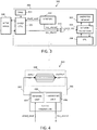
- Fig. 3 shows a block diagram 300 representing an illustrative embodiment of an integrated circuit.
- the integrated circuit comprises an active shield 108 and a security-critical IC component 106.
- the IC component 106 comprises a key store 302, an encrypted memory 304 (i.e., a memory containing encrypted content), a memory encryption block 306 which is operatively connected to the encrypted memory 304, and a central processing unit 308 which is operatively connected to the memory encryption block 306.
- the IC component 106 comprises an XOR gate 310 for performing exclusive-or operations.
- the IC component 106 comprises the shield controller 202 and a true random number generator 312 which is configured to provide true random bits to the shield controller 202.
- the shield controller 202 may mask the input value provided to the active shield 108 and unmask the output value of the active shield 108 using said true random bits, as will be explained in more detail with reference to Fig. 4 and Fig. 6 .
- the active shield 108 has a data input and a data output.
- the output value may be regarded as a deterministic mapping of the input value, denoted shield_map. In other words, as long as the conductive wires are intact, an input value which is transmitted through said wires produces a predictable output value.
- the size of the output value may match the size of the required decryption key.
- the memory encryption block 306 may be configured to encrypt the contents of the memory 304 using an encryption key and to decrypt the contents of the memory 304 using a corresponding decryption key. Furthermore, the decryption key may the same as the encryption key.
- the following data may be permanently stored in the key store 302: shield_seed (a random number generated once at the production time of the IC, i.e. a fixed random seed value) and key_share0 (another random number generated once at the production time of the IC, i.e. another fixed random number).
- the memory encryption block 306 may be controlled by the central processing unit 308.
- the output of the active shield 108 may be subject to an exclusive-or operation.
- the key store 302 and the encrypted memory 304 have been shown as separate blocks of the IC component 106, they may in fact reside in the same physical memory. In this way, IC area may be saved.
- the key store 302 may be a small area in said physical memory where no encryption takes place.
- the content of the key store 302 may be accessible by means of optical read-out, in order to access the encrypted memory content, an attacker also needs to know the mapping shield_map. However, this mapping is design information that may be kept secret by the IC manufacturer.
- the access key (e.g., mem_key ) is based on the output value (e.g., key_share1 ) of the active shield and on a fixed random number (e.g., key_share0 ).
- the security-critical component may be configured to generate the access key by performing an exclusive-or operation on the output value of the active shield and said fixed random number.
- the security-critical component is further configured to provide an input value to the active shield, said input value being based on a fixed random seed value (e.g., shield_seed ) . In this way, the resulting access key becomes again more complex.
- Fig. 4 shows a block diagram 400 illustrating how an active shield may be controlled in accordance with one or more embodiments.
- the active shield 108 may comprise a dense mesh of wires transporting random signals.
- the IC component may contain a shield controller 402 connected to an input 204 of the active shield 108 and connected to an output 206 of the active shield 108.
- the shield controller 402 may generate said random signals and may check their consistency in an attempt to detect damages to the conductive wires. Since the signals are random, it may in practice be difficult to implement the above-mentioned deterministic mapping ( shield_map ). Therefore, in one or more embodiments, the security-critical component is further configured to mask the input value with a variable random value before providing said input value to the active shield.
- the security-critical component is further configured to unmask the output value of the active shield using said variable random value.
- the signals transmitted through the conductive wires of the active shield 108 may be randomized sufficiently while keeping said deterministic mapping intact.
- the shield controller 402 is configured to mask the input value and unmask the output value.
- the shield controller 402 may comprise a masking unit 404 configured to mask the input value and an unmasking unit 406 configured to unmask the output value.
- Boolean masking may be used for masking the input value and unmasking the output value.
- the shield_map algorithm may require a bit to be in the state 'A'.
- the masking unit 404 may generate a random bit 'R' and set the associated shield line to 'A' XOR 'R'.
- the unmasking unit 406 retrieves 'A' by performing an XOR operation on the state on the line with 'R'.
- Other methods may be used for masking and unmasking, for example in order to increase the level of security and increase the overall efficiency.
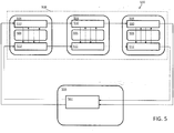
- Fig. 5 shows an illustrative embodiment of an active shield implementation 500.
- the active shield implementation 500 comprises a plurality of slices 504, and each slice 504 implements a linear function.
- Each slice 504 comprises a first logic unit 510, which comprises combinational logic and a memory, and a second logic unit 512, which comprises combinational logic and optionally a memory.
- Shield lines which are positioned above the protected area and in particular above the security-critical IC component 506, transport bits between the first logic unit 510 and the second logic unit 512.
- the shield controller 502 comprised in the security-critical component 506 is configured to provide serial data and control signals to the first logic unit 510 of the first slice (i.e. the left slice). Furthermore, the shield controller 502 is configured to provide serial data and optionally control signals to the second logic unit 512 of the first slice.
- the combinational logic performs transformations on the serial data under control of the control signals, thereby implementing the aforementioned linear function.
- Intermediate data may be stored in the memory comprised in the logic units 510, 512.
- the active shield may be grouped in slices and each slice may implement the same linear function.
- the shield controller 502 may drive the first slice and the data may be shifted through the slices; this process may be regarded as similar to the process executed by a shift register. Each slice, except the first slide, accepts as input the output of the previous slice. The shield controller 502 receives the output of the last slice (i.e. the right slice) and uses it to generate an access key of the kind set forth.
- the skilled person will appreciate that the number of slices can be different from the number shown; it is emphasized that Fig. 5 merely shows an example with a small number of slices in order to illustrate the principle.
- the linear function implemented by the slices may accept a plurality of input bits so as to produce a large number of intermediate values.
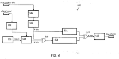
- Fig. 6 shows an illustrative embodiment of a data flow 600 of an active shield implementation.
- the data flow 600 comprises an active shield 608 which includes a slice function (referred to as a "linear slice function") based on a plurality of slices which implement a linear function, as described with reference to Fig. 5 . All other functional blocks in the data flow are implemented in the shield controller.
- a slice function referred to as a "linear slice function”
- those functional blocks comprise a set of elements involved in masking and unmasking the input value and the output value, respectively, of the active shield: a buffer 610 receiving true random bits as an input, a pseudo-random number generator 602 receiving input from said buffer 610, an XOR gate 618 receiving input from the pseudo-random number generator 602, a linear slice function 614 which corresponds to the linear slice function included in the active shield 608 and which receives input from the pseudo-random number generator 602, and an XOR gate 620 which receives input from the slice function 614 and the active shield 608.
- the data flow 600 comprises another pseudo-random number generator 602 which receives the seed value shield_seed as an input, an N-bit counter 606 which counts the number of input values provided to the slice function, an N-bit encryption function 604 which receives input from the pseudo-random number generator 602 and form the N-bit counter 606 and which sends its output to the XOR gate 618, and a hash function 616 receiving input from the XOR gate 620 and producing as output the output value key_share1.
- the data flow 600 may form part of a test procedure which effectively tests whether the active shield 608 has been damaged in order to determine whether the integrated circuit has been tampered with.
- a single pass may be defined as M steps of the pseudo-random number generators 602, 612.
- a single test may comprise 2 N passes, or 2 N ⁇ 2 passes if the slices use latches as memory elements; this number of passes makes sure that all possible input values are provided to the slice function and thus it represents the minimum amount of work which is required to produce the output value key_share1 while ensuring that all shield lines are intact.
- the pseudo-random number generators 602, 612 are reset (i.e., the seed of the pseudo-random number generators 602 is reloaded for each pass).
- the pseudo-random number generators 602, 612 produce a new random value, and for each slice the pseudo-random number generators 602, 612 produce such a new random value.
- the N-bit counter is reset to its initial value, and at each pass, the N-bit counter 606 (which may also be referred to as a pass counter) produces a new value (i.e., it is incremented).
- the active shield 608 has a serial data input, a serial data output and may be regarded as a shift register with M stages, wherein each stage involves a slice that is configured to shift N transformed bits to a next slice.
- the buffer 610, pseudo-random number generator 612 and slice function 614 do not operate on any data related to the seed value shield_seed but only operate on true random data; they are used for masking the input value to the active shield 608 and unmasking the output value of the active shield 608.
- the N-bit encryption function 604 is used to diversify the counter value in dependence on the seed value shield_seed.
- the N-bit encryption function 604 outputs a deterministic input for the active shield 608, which is masked by the output of the pseudo-random number generator 612 at the XOR gate 618. Accordingly, the XOR gate 618 outputs a random input for the active shield 608.
- the output of the active shield 608 is random, and is unmasked at the XOR gate 620. Accordingly, the XOR gate 620 outputs a deterministic input for the hash function 616.
- the security-critical component is configured to generate an error signal if the access to it is not enabled.
- the security-critical component 106 may generate an error signal which is output to a device external to the IC, for example. If a deterministic error signal is desired, the system may read at a special location in the encrypted memory 304 where a well-known value is stored. If the value is wide enough, for example 128 bits, the probability that the expected value is obtained with an incorrect decryption key is negligible.
- Another approach is to compute a cyclic redundancy check (CRC) over mem_key and compare it with an expected value stored in the key store 302.
- CRC cyclic redundancy check
Landscapes
- Engineering & Computer Science (AREA)
- Computer Security & Cryptography (AREA)
- Theoretical Computer Science (AREA)
- Computer Hardware Design (AREA)
- Physics & Mathematics (AREA)
- General Physics & Mathematics (AREA)
- General Engineering & Computer Science (AREA)
- Software Systems (AREA)
- Microelectronics & Electronic Packaging (AREA)
- Health & Medical Sciences (AREA)
- General Health & Medical Sciences (AREA)
- Computer Networks & Wireless Communication (AREA)
- Signal Processing (AREA)
- Bioethics (AREA)
- Social Psychology (AREA)
- Storage Device Security (AREA)
- Semiconductor Integrated Circuits (AREA)
Claims (9)
- Integrierte Schaltung (100), die ein Chip ist, wobei die integrierte Schaltung (100) eine aktive Schirmung (108) in einer ersten Schicht (102) und zumindest eine sicherheitskritische Komponente (106) in einer zweiten Schicht (104) umfasst, wobei die aktive Schirmung (108) einen Dateneingang, einen Datenausgang und mehrere metallische elektrische Verbindungen umfasst, die ausgelegt sind zum Senden eines Eingangswerts zum Produzieren eines Ausgangswerts, wobei die Verbindungen in die erste Schicht (102) eingebettet sind, wobei der Ausgangswert eine deterministische Abbildung des Eingangswerts ist, solange die metallischen elektrischen Verbindungen nicht beschädigt sind,
dadurch gekennzeichnet, dass die sicherheitskritische Komponente (106) ausgelegt ist zum Erzeugen eines Zugangsschlüssels zum Ermöglichen von Zugang für zumindest einen Teil der sicherheitskritischen Komponente (106), wobei der Zugangsschlüssel auf dem Ausgangswert der aktiven Schirmung (108) basiert,
wobei die sicherheitskritische Komponente (106) ferner ausgelegt ist zum Verwenden des Zugangsschlüssels zum Ermöglichen von Zugang zum Inhalt einer Speichereinheit (304), enthalten in der sicherheitskritischen Komponente (106), wobei der Zugangsschlüssel ein Passwort oder ein Entschlüsselungsschlüssel ist, der Zugang zum Inhalt ermöglicht, oder zum Entschlüsseln des Inhalts,
wobei die sicherheitskritische Komponente (106) ferner ausgelegt ist zum Bereitstellen eines Eingangswerts für die aktive Schirmung (108), wobei der Eingangswert auf einem festen Anfangswert basiert, zum Maskieren des Eingangswerts mit einem variablen zufälligen Wert vor Bereitstellen des Eingangswerts für die aktive Schirmung (108), und zum Demaskieren des Ausgangswerts der aktiven Schirmung (108) unter Verwendung des variablen zufälligen Werts. - Integrierte Schaltung (100) nach einem der vorhergehenden Ansprüche, wobei der Zugangsschlüssel auf dem Ausgangswert der aktiven Schirmung (108) und auf einer festen Zahl basiert.
- Integrierte Schaltung (100) nach Anspruch 2, wobei die sicherheitskritische Komponente (106) ferner ausgelegt ist zum Erzeugen des Zugangsschlüssels durch Durchführen einer Exklusiv-Oder-Operation auf dem Ausgangswert der aktiven Schirmung (108) und der festen Zahl.
- Integrierte Schaltung (100) nach Anspruch 1, wobei die sicherheitskritische Komponente (106) eine Schirmungssteuerung (202) umfasst, die ausgelegt ist zum Maskieren des Eingangswerts und Demaskieren des Ausgangswerts.
- Integrierte Schaltung (100) nach einem der vorhergehenden Ansprüche, wobei die sicherheitskritische Komponente (106) ferner ausgelegt ist zum Erzeugen eines Fehlersignals, wenn der Zugang nicht ermöglicht ist.
- Smartcard, umfassend eine integrierte Schaltung (100) nach einem der vorhergehenden Ansprüche.
- Elektronisches Identifizierungsdokument, umfassend eine integrierte Schaltung (100) nach einem der Ansprüche 1 bis 5.
- Verfahren zum Schutz einer integrierten Schaltung (100), die ein Chip ist, wobei die integrierte Schaltung (100) eine aktive Schirmung (108) in einer ersten Schicht (102) und zumindest eine sicherheitskritische Komponente (106) in einer zweiten Schicht (104) umfasst, wobei die aktive Schirmung (108) einen Dateneingang, einen Datenausgang und mehrere metallische elektrische Verbindungen umfasst, die ausgelegt sind zum Senden eines Eingangswerts zum Produzieren eines Ausgangswerts, wobei die Verbindungen in die erste Schicht (102) eingebettet sind, wobei der Ausgangswert eine deterministische Abbildung des Eingangswerts ist, solange die metallischen elektrischen Verbindungen nicht beschädigt sind,
dadurch gekennzeichnet, dass die sicherheitskritische Komponente (106) einen Zugangsschlüssel zum Ermöglichen von Zugang für zumindest einen Teil der sicherheitskritischen Komponente (106) erzeugt, und wobei der Zugangsschlüssel auf dem Ausgangswert der aktiven Schirmung (108) basiert,
wobei die sicherheitskritische Komponente (106) ferner den Zugangsschlüssel zum Ermöglichen von Zugang zum Inhalt einer Speichereinheit (304), enthalten in der sicherheitskritischen Komponente (106), wobei der Zugangsschlüssel ein Passwort oder ein Entschlüsselungsschlüssel ist, der Zugang zum Inhalt ermöglicht, oder zum Entschlüsseln des Inhalts verwendet,
wobei die sicherheitskritische Komponente (106) ferner einen Eingangswert für die aktive Schirmung (108) bereitstellt, wobei der Eingangswert auf einem festen Anfangswert basiert, den Eingangswert mit einem variablen zufälligen Wert vor Bereitstellen des Eingangswerts für die aktive Schirmung (108) maskiert und den Ausgangswert der aktiven Schirmung (108) unter Verwendung des variablen zufälligen Werts demaskiert. - Computerprogrammprodukt, umfassend Anweisungen, die, wenn durch eine sicherheitskritische Komponente (106) einer integrierten Schaltung (100) ausgeführt, die sicherheitskritische Komponente (106) veranlassen, ein Verfahren nach Anspruch 8 auszuführen.
Priority Applications (5)
| Application Number | Priority Date | Filing Date | Title |
|---|---|---|---|
| EP15290240.9A EP3147830B1 (de) | 2015-09-23 | 2015-09-23 | Schutz fuer eine integrierte schaltung |
| JP2016137595A JP6792970B2 (ja) | 2015-09-23 | 2016-07-12 | 集積回路、集積回路を保護する方法及びコンピュータプログラム製品 |
| CN201610794230.9A CN106548100B (zh) | 2015-09-23 | 2016-08-31 | 集成电路以及用于保护集成电路的方法 |
| US15/268,462 US10282312B2 (en) | 2015-09-23 | 2016-09-16 | Integrated circuit, method for protecting an integrated circuit and computer program product |
| KR1020160122178A KR102729574B1 (ko) | 2015-09-23 | 2016-09-23 | 접적 회로, 접적 회로를 보호하는 방법 및 컴퓨터 프로그램 제품 |
Applications Claiming Priority (1)
| Application Number | Priority Date | Filing Date | Title |
|---|---|---|---|
| EP15290240.9A EP3147830B1 (de) | 2015-09-23 | 2015-09-23 | Schutz fuer eine integrierte schaltung |
Publications (2)
| Publication Number | Publication Date |
|---|---|
| EP3147830A1 EP3147830A1 (de) | 2017-03-29 |
| EP3147830B1 true EP3147830B1 (de) | 2020-11-18 |
Family
ID=54476874
Family Applications (1)
| Application Number | Title | Priority Date | Filing Date |
|---|---|---|---|
| EP15290240.9A Active EP3147830B1 (de) | 2015-09-23 | 2015-09-23 | Schutz fuer eine integrierte schaltung |
Country Status (5)
| Country | Link |
|---|---|
| US (1) | US10282312B2 (de) |
| EP (1) | EP3147830B1 (de) |
| JP (1) | JP6792970B2 (de) |
| KR (1) | KR102729574B1 (de) |
| CN (1) | CN106548100B (de) |
Families Citing this family (8)
| Publication number | Priority date | Publication date | Assignee | Title |
|---|---|---|---|---|
| JP7216645B2 (ja) * | 2016-12-05 | 2023-02-01 | クリプトグラフィ リサーチ, インコーポレイテッド | 裏面セキュリティ・シールド |
| US10573605B2 (en) * | 2016-12-13 | 2020-02-25 | University Of Florida Research Foundation, Incorporated | Layout-driven method to assess vulnerability of ICs to microprobing attacks |
| CN108733311B (zh) * | 2017-04-17 | 2021-09-10 | 伊姆西Ip控股有限责任公司 | 用于管理存储系统的方法和设备 |
| US10798075B2 (en) * | 2018-01-29 | 2020-10-06 | International Business Machines Corporation | Interface layer obfuscation and usage thereof |
| CN109100635B (zh) * | 2018-07-11 | 2021-06-29 | 北京智芯微电子科技有限公司 | 对多通道金属屏蔽布线层进行完整性检测的电路及方法 |
| US10839109B2 (en) * | 2018-11-14 | 2020-11-17 | Massachusetts Institute Of Technology | Integrated circuit (IC) portholes and related techniques |
| US11343672B2 (en) | 2019-02-20 | 2022-05-24 | Coretigo Ltd. | Secure communication encryption and decryption mechanism in a wireless communication system |
| US12039091B2 (en) * | 2021-10-07 | 2024-07-16 | Duke University | Integrated circuit protections against removal and oracle-guided attacks |
Citations (2)
| Publication number | Priority date | Publication date | Assignee | Title |
|---|---|---|---|---|
| US6962294B2 (en) * | 2002-05-24 | 2005-11-08 | Infineon Technologie Ag | Integrated circuit having an active shield |
| US20120117645A1 (en) * | 2010-11-05 | 2012-05-10 | Ji Myung Na | Detection circuit, detection method thereof, and memory system including the detection circuit |
Family Cites Families (24)
| Publication number | Priority date | Publication date | Assignee | Title |
|---|---|---|---|---|
| FR2738971B1 (fr) * | 1995-09-19 | 1997-10-10 | Schlumberger Ind Sa | Procede de determination d'une cle de cryptage associee a un circuit integre |
| AT408925B (de) * | 1996-10-22 | 2002-04-25 | Posch Reinhard Dr | Anordnung zum schutz von elektronischen recheneinheiten, insbesondere von chipkarten |
| US7005733B2 (en) | 1999-12-30 | 2006-02-28 | Koemmerling Oliver | Anti tamper encapsulation for an integrated circuit |
| ATE350766T1 (de) * | 2000-08-21 | 2007-01-15 | Infineon Technologies Ag | Vorrichtung zum schutz einer integrierten schaltung |
| DE10044837C1 (de) | 2000-09-11 | 2001-09-13 | Infineon Technologies Ag | Schaltungsanordnung und Verfahren zum Detektieren eines unerwünschten Angriffs auf eine integrierte Schaltung |
| FR2864667B1 (fr) | 2003-12-29 | 2006-02-24 | Commissariat Energie Atomique | Protection d'une puce de circuit integre contenant des donnees confidentielles |
| CN1922564B (zh) | 2004-02-24 | 2011-01-26 | Nxp股份有限公司 | Ic侵入检测 |
| WO2007086046A2 (en) | 2006-01-24 | 2007-08-02 | Nds Limited | Chip attack protection |
| US20090024890A1 (en) * | 2006-02-09 | 2009-01-22 | Nxp B.V. | Circuit arrangement, data processing device comprising such circuit arrangement as well as method for identifying an attack on such circuit arrangement |
| JP4349389B2 (ja) * | 2006-07-28 | 2009-10-21 | ソニー株式会社 | データ記憶装置、および、通信装置 |
| KR101299602B1 (ko) | 2007-03-27 | 2013-08-26 | 삼성전자주식회사 | 리버스 엔지니어링을 보호하는 집적회로 |
| TWI505686B (zh) * | 2009-09-29 | 2015-10-21 | 滿捷特科技公司 | 具有有限加密鑰取回的通訊系統、方法及裝置 |
| US8610454B2 (en) | 2010-01-12 | 2013-12-17 | Stc.Unm | System and methods for generating unclonable security keys in integrated circuits |
| US20130141137A1 (en) | 2011-06-01 | 2013-06-06 | ISC8 Inc. | Stacked Physically Uncloneable Function Sense and Respond Module |
| JP2013045407A (ja) * | 2011-08-26 | 2013-03-04 | Renesas Electronics Corp | 半導体装置 |
| WO2013072897A2 (en) * | 2011-11-18 | 2013-05-23 | Tubitak | Active shield with electrically configurable interconnections |
| US9323950B2 (en) * | 2012-07-19 | 2016-04-26 | Atmel Corporation | Generating signatures using a secure device |
| US10771448B2 (en) * | 2012-08-10 | 2020-09-08 | Cryptography Research, Inc. | Secure feature and key management in integrated circuits |
| KR20140034332A (ko) | 2012-08-14 | 2014-03-20 | 삼성전자주식회사 | 보안 장치 및 이를 구비하는 집적 회로 |
| CN104704768B (zh) * | 2012-10-04 | 2018-01-05 | 本质Id有限责任公司 | 用于从用作物理不可克隆功能的存储器中生成密码密钥的系统 |
| EP2819049B1 (de) | 2013-06-27 | 2015-11-18 | Nxp B.V. | Vorrichtung mit kapazitivem Sicherheitsschild |
| US9171810B2 (en) * | 2013-11-21 | 2015-10-27 | Nxp B.V. | Electronic device incorporating a randomized interconnection layer having a randomized conduction pattern |
| CN103646137A (zh) * | 2013-12-03 | 2014-03-19 | 北京中电华大电子设计有限责任公司 | 一种高安全芯片有源屏蔽物理保护结构的设计方法 |
| CN104268049B (zh) * | 2014-09-30 | 2017-01-25 | 北京金山安全软件有限公司 | 判断存储设备异常的方法、装置及终端 |
-
2015
- 2015-09-23 EP EP15290240.9A patent/EP3147830B1/de active Active
-
2016
- 2016-07-12 JP JP2016137595A patent/JP6792970B2/ja active Active
- 2016-08-31 CN CN201610794230.9A patent/CN106548100B/zh active Active
- 2016-09-16 US US15/268,462 patent/US10282312B2/en active Active
- 2016-09-23 KR KR1020160122178A patent/KR102729574B1/ko active Active
Patent Citations (2)
| Publication number | Priority date | Publication date | Assignee | Title |
|---|---|---|---|---|
| US6962294B2 (en) * | 2002-05-24 | 2005-11-08 | Infineon Technologie Ag | Integrated circuit having an active shield |
| US20120117645A1 (en) * | 2010-11-05 | 2012-05-10 | Ji Myung Na | Detection circuit, detection method thereof, and memory system including the detection circuit |
Also Published As
| Publication number | Publication date |
|---|---|
| US20170083459A1 (en) | 2017-03-23 |
| JP6792970B2 (ja) | 2020-12-02 |
| CN106548100A (zh) | 2017-03-29 |
| CN106548100B (zh) | 2021-11-02 |
| KR20170035820A (ko) | 2017-03-31 |
| KR102729574B1 (ko) | 2024-11-12 |
| EP3147830A1 (de) | 2017-03-29 |
| US10282312B2 (en) | 2019-05-07 |
| JP2017063401A (ja) | 2017-03-30 |
Similar Documents
| Publication | Publication Date | Title |
|---|---|---|
| US10282312B2 (en) | Integrated circuit, method for protecting an integrated circuit and computer program product | |
| EP3454318B1 (de) | Sicherheitssystem mit entropy bits, die von einer puf generiert werden | |
| US12333056B2 (en) | Neural network cryptography coprocessor providing countermeasture against side-channel analysis | |
| Cui et al. | A new PUF based lock and key solution for secure in-field testing of cryptographic chips | |
| CN112930659B (zh) | 用于安全密钥生成的方法和设备 | |
| EP2336930B1 (de) | Verfahren und Vorrichtung zur Detektion eines Fehlerinjektion | |
| US10025954B2 (en) | Method for operating a control unit | |
| Chen et al. | Hardware protection via logic locking test points | |
| Kean et al. | Verifying the authenticity of chip designs with the DesignTag system | |
| Hamdioui et al. | Hacking and protecting IC hardware | |
| Dubrova et al. | Keyed logic BIST for Trojan detection in SoC | |
| Jang et al. | PASS: Pattern-sequence-authentication-based secure scan against reverse engineering attacks | |
| US10992464B2 (en) | Chip and method for securely storing secret data | |
| Suzano et al. | Enhancing dft security in chiplet-based systems with encryption and integrity checking | |
| Lemke | Embedded security: Physical protection against tampering attacks | |
| Kaur et al. | Analytical classifications of side channel attacks, glitch attacks and fault injection techniques: their countermeasures | |
| US10514892B2 (en) | Apparatus and method for detecting integrity violation | |
| Lemke-Rust | Models and algorithms for physical cryptanalysis | |
| EP3642820B1 (de) | Datenverarbeitungsvorrichtung zur verarbeitung erweiterter daten | |
| Salmani et al. | Special session: Countering IP security threats in supply chain | |
| EP3817273A1 (de) | Leistungsverbesserung eines kryptographischen moduls einer integrierten schaltung | |
| Jang et al. | Evolution of Obfuscation-Based Scan Design Techniques | |
| Rosinskiy et al. | Agent-Oriented Approach to Detect Hardware Trojans | |
| Jack Harper | CRYPTOGRAPHICALLY SECURE TRANSACTIONS WITH OPTICAL CARDS | |
| Moein | Systematic analysis and methodologies for hardware security |
Legal Events
| Date | Code | Title | Description |
|---|---|---|---|
| PUAI | Public reference made under article 153(3) epc to a published international application that has entered the european phase |
Free format text: ORIGINAL CODE: 0009012 |
|
| STAA | Information on the status of an ep patent application or granted ep patent |
Free format text: STATUS: THE APPLICATION HAS BEEN PUBLISHED |
|
| AK | Designated contracting states |
Kind code of ref document: A1 Designated state(s): AL AT BE BG CH CY CZ DE DK EE ES FI FR GB GR HR HU IE IS IT LI LT LU LV MC MK MT NL NO PL PT RO RS SE SI SK SM TR |
|
| AX | Request for extension of the european patent |
Extension state: BA ME |
|
| STAA | Information on the status of an ep patent application or granted ep patent |
Free format text: STATUS: REQUEST FOR EXAMINATION WAS MADE |
|
| 17P | Request for examination filed |
Effective date: 20170929 |
|
| RBV | Designated contracting states (corrected) |
Designated state(s): AL AT BE BG CH CY CZ DE DK EE ES FI FR GB GR HR HU IE IS IT LI LT LU LV MC MK MT NL NO PL PT RO RS SE SI SK SM TR |
|
| STAA | Information on the status of an ep patent application or granted ep patent |
Free format text: STATUS: EXAMINATION IS IN PROGRESS |
|
| 17Q | First examination report despatched |
Effective date: 20180920 |
|
| GRAP | Despatch of communication of intention to grant a patent |
Free format text: ORIGINAL CODE: EPIDOSNIGR1 |
|
| STAA | Information on the status of an ep patent application or granted ep patent |
Free format text: STATUS: GRANT OF PATENT IS INTENDED |
|
| INTG | Intention to grant announced |
Effective date: 20200629 |
|
| GRAS | Grant fee paid |
Free format text: ORIGINAL CODE: EPIDOSNIGR3 |
|
| GRAA | (expected) grant |
Free format text: ORIGINAL CODE: 0009210 |
|
| STAA | Information on the status of an ep patent application or granted ep patent |
Free format text: STATUS: THE PATENT HAS BEEN GRANTED |
|
| AK | Designated contracting states |
Kind code of ref document: B1 Designated state(s): AL AT BE BG CH CY CZ DE DK EE ES FI FR GB GR HR HU IE IS IT LI LT LU LV MC MK MT NL NO PL PT RO RS SE SI SK SM TR |
|
| REG | Reference to a national code |
Ref country code: GB Ref legal event code: FG4D |
|
| REG | Reference to a national code |
Ref country code: CH Ref legal event code: EP |
|
| REG | Reference to a national code |
Ref country code: DE Ref legal event code: R096 Ref document number: 602015062092 Country of ref document: DE |
|
| REG | Reference to a national code |
Ref country code: IE Ref legal event code: FG4D |
|
| REG | Reference to a national code |
Ref country code: AT Ref legal event code: REF Ref document number: 1336574 Country of ref document: AT Kind code of ref document: T Effective date: 20201215 |
|
| REG | Reference to a national code |
Ref country code: AT Ref legal event code: MK05 Ref document number: 1336574 Country of ref document: AT Kind code of ref document: T Effective date: 20201118 |
|
| REG | Reference to a national code |
Ref country code: NL Ref legal event code: MP Effective date: 20201118 |
|
| PG25 | Lapsed in a contracting state [announced via postgrant information from national office to epo] |
Ref country code: GR Free format text: LAPSE BECAUSE OF FAILURE TO SUBMIT A TRANSLATION OF THE DESCRIPTION OR TO PAY THE FEE WITHIN THE PRESCRIBED TIME-LIMIT Effective date: 20210219 Ref country code: RS Free format text: LAPSE BECAUSE OF FAILURE TO SUBMIT A TRANSLATION OF THE DESCRIPTION OR TO PAY THE FEE WITHIN THE PRESCRIBED TIME-LIMIT Effective date: 20201118 Ref country code: FI Free format text: LAPSE BECAUSE OF FAILURE TO SUBMIT A TRANSLATION OF THE DESCRIPTION OR TO PAY THE FEE WITHIN THE PRESCRIBED TIME-LIMIT Effective date: 20201118 Ref country code: NO Free format text: LAPSE BECAUSE OF FAILURE TO SUBMIT A TRANSLATION OF THE DESCRIPTION OR TO PAY THE FEE WITHIN THE PRESCRIBED TIME-LIMIT Effective date: 20210218 Ref country code: PT Free format text: LAPSE BECAUSE OF FAILURE TO SUBMIT A TRANSLATION OF THE DESCRIPTION OR TO PAY THE FEE WITHIN THE PRESCRIBED TIME-LIMIT Effective date: 20210318 |
|
| PG25 | Lapsed in a contracting state [announced via postgrant information from national office to epo] |
Ref country code: LV Free format text: LAPSE BECAUSE OF FAILURE TO SUBMIT A TRANSLATION OF THE DESCRIPTION OR TO PAY THE FEE WITHIN THE PRESCRIBED TIME-LIMIT Effective date: 20201118 Ref country code: SE Free format text: LAPSE BECAUSE OF FAILURE TO SUBMIT A TRANSLATION OF THE DESCRIPTION OR TO PAY THE FEE WITHIN THE PRESCRIBED TIME-LIMIT Effective date: 20201118 Ref country code: PL Free format text: LAPSE BECAUSE OF FAILURE TO SUBMIT A TRANSLATION OF THE DESCRIPTION OR TO PAY THE FEE WITHIN THE PRESCRIBED TIME-LIMIT Effective date: 20201118 Ref country code: IS Free format text: LAPSE BECAUSE OF FAILURE TO SUBMIT A TRANSLATION OF THE DESCRIPTION OR TO PAY THE FEE WITHIN THE PRESCRIBED TIME-LIMIT Effective date: 20210318 Ref country code: BG Free format text: LAPSE BECAUSE OF FAILURE TO SUBMIT A TRANSLATION OF THE DESCRIPTION OR TO PAY THE FEE WITHIN THE PRESCRIBED TIME-LIMIT Effective date: 20210218 Ref country code: AT Free format text: LAPSE BECAUSE OF FAILURE TO SUBMIT A TRANSLATION OF THE DESCRIPTION OR TO PAY THE FEE WITHIN THE PRESCRIBED TIME-LIMIT Effective date: 20201118 |
|
| REG | Reference to a national code |
Ref country code: LT Ref legal event code: MG9D |
|
| PG25 | Lapsed in a contracting state [announced via postgrant information from national office to epo] |
Ref country code: HR Free format text: LAPSE BECAUSE OF FAILURE TO SUBMIT A TRANSLATION OF THE DESCRIPTION OR TO PAY THE FEE WITHIN THE PRESCRIBED TIME-LIMIT Effective date: 20201118 |
|
| PG25 | Lapsed in a contracting state [announced via postgrant information from national office to epo] |
Ref country code: LT Free format text: LAPSE BECAUSE OF FAILURE TO SUBMIT A TRANSLATION OF THE DESCRIPTION OR TO PAY THE FEE WITHIN THE PRESCRIBED TIME-LIMIT Effective date: 20201118 Ref country code: SK Free format text: LAPSE BECAUSE OF FAILURE TO SUBMIT A TRANSLATION OF THE DESCRIPTION OR TO PAY THE FEE WITHIN THE PRESCRIBED TIME-LIMIT Effective date: 20201118 Ref country code: RO Free format text: LAPSE BECAUSE OF FAILURE TO SUBMIT A TRANSLATION OF THE DESCRIPTION OR TO PAY THE FEE WITHIN THE PRESCRIBED TIME-LIMIT Effective date: 20201118 Ref country code: SM Free format text: LAPSE BECAUSE OF FAILURE TO SUBMIT A TRANSLATION OF THE DESCRIPTION OR TO PAY THE FEE WITHIN THE PRESCRIBED TIME-LIMIT Effective date: 20201118 Ref country code: EE Free format text: LAPSE BECAUSE OF FAILURE TO SUBMIT A TRANSLATION OF THE DESCRIPTION OR TO PAY THE FEE WITHIN THE PRESCRIBED TIME-LIMIT Effective date: 20201118 Ref country code: CZ Free format text: LAPSE BECAUSE OF FAILURE TO SUBMIT A TRANSLATION OF THE DESCRIPTION OR TO PAY THE FEE WITHIN THE PRESCRIBED TIME-LIMIT Effective date: 20201118 |
|
| REG | Reference to a national code |
Ref country code: DE Ref legal event code: R097 Ref document number: 602015062092 Country of ref document: DE |
|
| PG25 | Lapsed in a contracting state [announced via postgrant information from national office to epo] |
Ref country code: DK Free format text: LAPSE BECAUSE OF FAILURE TO SUBMIT A TRANSLATION OF THE DESCRIPTION OR TO PAY THE FEE WITHIN THE PRESCRIBED TIME-LIMIT Effective date: 20201118 |
|
| PLBE | No opposition filed within time limit |
Free format text: ORIGINAL CODE: 0009261 |
|
| STAA | Information on the status of an ep patent application or granted ep patent |
Free format text: STATUS: NO OPPOSITION FILED WITHIN TIME LIMIT |
|
| 26N | No opposition filed |
Effective date: 20210819 |
|
| PG25 | Lapsed in a contracting state [announced via postgrant information from national office to epo] |
Ref country code: NL Free format text: LAPSE BECAUSE OF FAILURE TO SUBMIT A TRANSLATION OF THE DESCRIPTION OR TO PAY THE FEE WITHIN THE PRESCRIBED TIME-LIMIT Effective date: 20201118 Ref country code: AL Free format text: LAPSE BECAUSE OF FAILURE TO SUBMIT A TRANSLATION OF THE DESCRIPTION OR TO PAY THE FEE WITHIN THE PRESCRIBED TIME-LIMIT Effective date: 20201118 Ref country code: IT Free format text: LAPSE BECAUSE OF FAILURE TO SUBMIT A TRANSLATION OF THE DESCRIPTION OR TO PAY THE FEE WITHIN THE PRESCRIBED TIME-LIMIT Effective date: 20201118 |
|
| PG25 | Lapsed in a contracting state [announced via postgrant information from national office to epo] |
Ref country code: ES Free format text: LAPSE BECAUSE OF FAILURE TO SUBMIT A TRANSLATION OF THE DESCRIPTION OR TO PAY THE FEE WITHIN THE PRESCRIBED TIME-LIMIT Effective date: 20201118 Ref country code: SI Free format text: LAPSE BECAUSE OF FAILURE TO SUBMIT A TRANSLATION OF THE DESCRIPTION OR TO PAY THE FEE WITHIN THE PRESCRIBED TIME-LIMIT Effective date: 20201118 |
|
| REG | Reference to a national code |
Ref country code: CH Ref legal event code: PL |
|
| REG | Reference to a national code |
Ref country code: BE Ref legal event code: MM Effective date: 20210930 |
|
| PG25 | Lapsed in a contracting state [announced via postgrant information from national office to epo] |
Ref country code: IS Free format text: LAPSE BECAUSE OF FAILURE TO SUBMIT A TRANSLATION OF THE DESCRIPTION OR TO PAY THE FEE WITHIN THE PRESCRIBED TIME-LIMIT Effective date: 20210318 Ref country code: MC Free format text: LAPSE BECAUSE OF FAILURE TO SUBMIT A TRANSLATION OF THE DESCRIPTION OR TO PAY THE FEE WITHIN THE PRESCRIBED TIME-LIMIT Effective date: 20201118 |
|
| PG25 | Lapsed in a contracting state [announced via postgrant information from national office to epo] |
Ref country code: LU Free format text: LAPSE BECAUSE OF NON-PAYMENT OF DUE FEES Effective date: 20210923 Ref country code: IE Free format text: LAPSE BECAUSE OF NON-PAYMENT OF DUE FEES Effective date: 20210923 Ref country code: BE Free format text: LAPSE BECAUSE OF NON-PAYMENT OF DUE FEES Effective date: 20210930 |
|
| PG25 | Lapsed in a contracting state [announced via postgrant information from national office to epo] |
Ref country code: LI Free format text: LAPSE BECAUSE OF NON-PAYMENT OF DUE FEES Effective date: 20210930 Ref country code: CH Free format text: LAPSE BECAUSE OF NON-PAYMENT OF DUE FEES Effective date: 20210930 |
|
| PG25 | Lapsed in a contracting state [announced via postgrant information from national office to epo] |
Ref country code: HU Free format text: LAPSE BECAUSE OF FAILURE TO SUBMIT A TRANSLATION OF THE DESCRIPTION OR TO PAY THE FEE WITHIN THE PRESCRIBED TIME-LIMIT; INVALID AB INITIO Effective date: 20150923 |
|
| PG25 | Lapsed in a contracting state [announced via postgrant information from national office to epo] |
Ref country code: CY Free format text: LAPSE BECAUSE OF FAILURE TO SUBMIT A TRANSLATION OF THE DESCRIPTION OR TO PAY THE FEE WITHIN THE PRESCRIBED TIME-LIMIT Effective date: 20201118 |
|
| P01 | Opt-out of the competence of the unified patent court (upc) registered |
Effective date: 20230725 |
|
| PG25 | Lapsed in a contracting state [announced via postgrant information from national office to epo] |
Ref country code: MK Free format text: LAPSE BECAUSE OF FAILURE TO SUBMIT A TRANSLATION OF THE DESCRIPTION OR TO PAY THE FEE WITHIN THE PRESCRIBED TIME-LIMIT Effective date: 20201118 |
|
| PG25 | Lapsed in a contracting state [announced via postgrant information from national office to epo] |
Ref country code: MT Free format text: LAPSE BECAUSE OF FAILURE TO SUBMIT A TRANSLATION OF THE DESCRIPTION OR TO PAY THE FEE WITHIN THE PRESCRIBED TIME-LIMIT Effective date: 20201118 |
|
| PGFP | Annual fee paid to national office [announced via postgrant information from national office to epo] |
Ref country code: DE Payment date: 20250820 Year of fee payment: 11 |
|
| PGFP | Annual fee paid to national office [announced via postgrant information from national office to epo] |
Ref country code: GB Payment date: 20250822 Year of fee payment: 11 |
|
| PGFP | Annual fee paid to national office [announced via postgrant information from national office to epo] |
Ref country code: FR Payment date: 20250821 Year of fee payment: 11 |
|
| PG25 | Lapsed in a contracting state [announced via postgrant information from national office to epo] |
Ref country code: TR Free format text: LAPSE BECAUSE OF FAILURE TO SUBMIT A TRANSLATION OF THE DESCRIPTION OR TO PAY THE FEE WITHIN THE PRESCRIBED TIME-LIMIT Effective date: 20201118 |