EP3148100B1 - Dispositif d'amplification avec des étages d'amplification doté d'un étage de traitement et de soas polarisées permettant d'amplifier des signaux optiques dans un système de transmission wdm - Google Patents
Dispositif d'amplification avec des étages d'amplification doté d'un étage de traitement et de soas polarisées permettant d'amplifier des signaux optiques dans un système de transmission wdm Download PDFInfo
- Publication number
- EP3148100B1 EP3148100B1 EP15306493.6A EP15306493A EP3148100B1 EP 3148100 B1 EP3148100 B1 EP 3148100B1 EP 15306493 A EP15306493 A EP 15306493A EP 3148100 B1 EP3148100 B1 EP 3148100B1
- Authority
- EP
- European Patent Office
- Prior art keywords
- optical
- optical signal
- amplification
- amplification stage
- polarized
- Prior art date
- Legal status (The legal status is an assumption and is not a legal conclusion. Google has not performed a legal analysis and makes no representation as to the accuracy of the status listed.)
- Not-in-force
Links
- 230000003287 optical effect Effects 0.000 title claims description 220
- 230000003321 amplification Effects 0.000 title claims description 108
- 238000003199 nucleic acid amplification method Methods 0.000 title claims description 108
- 230000005540 biological transmission Effects 0.000 title description 13
- 230000010287 polarization Effects 0.000 claims description 62
- 239000004065 semiconductor Substances 0.000 claims description 27
- 230000009466 transformation Effects 0.000 claims description 24
- 239000000463 material Substances 0.000 claims description 10
- 230000001131 transforming effect Effects 0.000 claims description 10
- 230000001419 dependent effect Effects 0.000 claims description 5
- 239000013307 optical fiber Substances 0.000 description 5
- 230000000295 complement effect Effects 0.000 description 4
- 239000013078 crystal Substances 0.000 description 4
- 239000010453 quartz Substances 0.000 description 4
- VYPSYNLAJGMNEJ-UHFFFAOYSA-N silicon dioxide Inorganic materials O=[Si]=O VYPSYNLAJGMNEJ-UHFFFAOYSA-N 0.000 description 4
- 238000010586 diagram Methods 0.000 description 3
- 230000008878 coupling Effects 0.000 description 2
- 238000010168 coupling process Methods 0.000 description 2
- 238000005859 coupling reaction Methods 0.000 description 2
- 230000001939 inductive effect Effects 0.000 description 2
- 230000003595 spectral effect Effects 0.000 description 2
- 229910052691 Erbium Inorganic materials 0.000 description 1
- 230000000694 effects Effects 0.000 description 1
- UYAHIZSMUZPPFV-UHFFFAOYSA-N erbium Chemical compound [Er] UYAHIZSMUZPPFV-UHFFFAOYSA-N 0.000 description 1
- 239000000835 fiber Substances 0.000 description 1
- 238000000034 method Methods 0.000 description 1
- 238000007493 shaping process Methods 0.000 description 1
Images

Classifications
-
- H—ELECTRICITY
- H01—ELECTRIC ELEMENTS
- H01S—DEVICES USING THE PROCESS OF LIGHT AMPLIFICATION BY STIMULATED EMISSION OF RADIATION [LASER] TO AMPLIFY OR GENERATE LIGHT; DEVICES USING STIMULATED EMISSION OF ELECTROMAGNETIC RADIATION IN WAVE RANGES OTHER THAN OPTICAL
- H01S5/00—Semiconductor lasers
- H01S5/50—Amplifier structures not provided for in groups H01S5/02 - H01S5/30
- H01S5/5036—Amplifier structures not provided for in groups H01S5/02 - H01S5/30 the arrangement being polarisation-selective
-
- H—ELECTRICITY
- H01—ELECTRIC ELEMENTS
- H01S—DEVICES USING THE PROCESS OF LIGHT AMPLIFICATION BY STIMULATED EMISSION OF RADIATION [LASER] TO AMPLIFY OR GENERATE LIGHT; DEVICES USING STIMULATED EMISSION OF ELECTROMAGNETIC RADIATION IN WAVE RANGES OTHER THAN OPTICAL
- H01S5/00—Semiconductor lasers
- H01S5/06—Arrangements for controlling the laser output parameters, e.g. by operating on the active medium
- H01S5/068—Stabilisation of laser output parameters
- H01S5/0683—Stabilisation of laser output parameters by monitoring the optical output parameters
-
- H—ELECTRICITY
- H01—ELECTRIC ELEMENTS
- H01S—DEVICES USING THE PROCESS OF LIGHT AMPLIFICATION BY STIMULATED EMISSION OF RADIATION [LASER] TO AMPLIFY OR GENERATE LIGHT; DEVICES USING STIMULATED EMISSION OF ELECTROMAGNETIC RADIATION IN WAVE RANGES OTHER THAN OPTICAL
- H01S5/00—Semiconductor lasers
- H01S5/40—Arrangement of two or more semiconductor lasers, not provided for in groups H01S5/02 - H01S5/30
- H01S5/4025—Array arrangements, e.g. constituted by discrete laser diodes or laser bar
- H01S5/4087—Array arrangements, e.g. constituted by discrete laser diodes or laser bar emitting more than one wavelength
-
- H—ELECTRICITY
- H01—ELECTRIC ELEMENTS
- H01S—DEVICES USING THE PROCESS OF LIGHT AMPLIFICATION BY STIMULATED EMISSION OF RADIATION [LASER] TO AMPLIFY OR GENERATE LIGHT; DEVICES USING STIMULATED EMISSION OF ELECTROMAGNETIC RADIATION IN WAVE RANGES OTHER THAN OPTICAL
- H01S5/00—Semiconductor lasers
- H01S5/50—Amplifier structures not provided for in groups H01S5/02 - H01S5/30
- H01S5/5009—Amplifier structures not provided for in groups H01S5/02 - H01S5/30 the arrangement being polarisation-insensitive
-
- H—ELECTRICITY
- H01—ELECTRIC ELEMENTS
- H01S—DEVICES USING THE PROCESS OF LIGHT AMPLIFICATION BY STIMULATED EMISSION OF RADIATION [LASER] TO AMPLIFY OR GENERATE LIGHT; DEVICES USING STIMULATED EMISSION OF ELECTROMAGNETIC RADIATION IN WAVE RANGES OTHER THAN OPTICAL
- H01S5/00—Semiconductor lasers
- H01S5/50—Amplifier structures not provided for in groups H01S5/02 - H01S5/30
- H01S5/5027—Concatenated amplifiers, i.e. amplifiers in series or cascaded
-
- H—ELECTRICITY
- H01—ELECTRIC ELEMENTS
- H01S—DEVICES USING THE PROCESS OF LIGHT AMPLIFICATION BY STIMULATED EMISSION OF RADIATION [LASER] TO AMPLIFY OR GENERATE LIGHT; DEVICES USING STIMULATED EMISSION OF ELECTROMAGNETIC RADIATION IN WAVE RANGES OTHER THAN OPTICAL
- H01S5/00—Semiconductor lasers
- H01S5/50—Amplifier structures not provided for in groups H01S5/02 - H01S5/30
- H01S5/5045—Amplifier structures not provided for in groups H01S5/02 - H01S5/30 the arrangement having a frequency filtering function
-
- H—ELECTRICITY
- H04—ELECTRIC COMMUNICATION TECHNIQUE
- H04B—TRANSMISSION
- H04B10/00—Transmission systems employing electromagnetic waves other than radio-waves, e.g. infrared, visible or ultraviolet light, or employing corpuscular radiation, e.g. quantum communication
- H04B10/29—Repeaters
- H04B10/291—Repeaters in which processing or amplification is carried out without conversion of the main signal from optical form
- H04B10/2912—Repeaters in which processing or amplification is carried out without conversion of the main signal from optical form characterised by the medium used for amplification or processing
- H04B10/2914—Repeaters in which processing or amplification is carried out without conversion of the main signal from optical form characterised by the medium used for amplification or processing using lumped semiconductor optical amplifiers [SOA]
-
- H—ELECTRICITY
- H04—ELECTRIC COMMUNICATION TECHNIQUE
- H04B—TRANSMISSION
- H04B10/00—Transmission systems employing electromagnetic waves other than radio-waves, e.g. infrared, visible or ultraviolet light, or employing corpuscular radiation, e.g. quantum communication
- H04B10/29—Repeaters
- H04B10/291—Repeaters in which processing or amplification is carried out without conversion of the main signal from optical form
- H04B10/293—Signal power control
- H04B10/294—Signal power control in a multiwavelength system, e.g. gain equalisation
-
- H—ELECTRICITY
- H04—ELECTRIC COMMUNICATION TECHNIQUE
- H04J—MULTIPLEX COMMUNICATION
- H04J14/00—Optical multiplex systems
- H04J14/02—Wavelength-division multiplex systems
- H04J14/0221—Power control, e.g. to keep the total optical power constant
-
- H—ELECTRICITY
- H04—ELECTRIC COMMUNICATION TECHNIQUE
- H04J—MULTIPLEX COMMUNICATION
- H04J14/00—Optical multiplex systems
- H04J14/06—Polarisation multiplex systems
-
- H—ELECTRICITY
- H01—ELECTRIC ELEMENTS
- H01S—DEVICES USING THE PROCESS OF LIGHT AMPLIFICATION BY STIMULATED EMISSION OF RADIATION [LASER] TO AMPLIFY OR GENERATE LIGHT; DEVICES USING STIMULATED EMISSION OF ELECTROMAGNETIC RADIATION IN WAVE RANGES OTHER THAN OPTICAL
- H01S2301/00—Functional characteristics
- H01S2301/04—Gain spectral shaping, flattening
-
- H—ELECTRICITY
- H01—ELECTRIC ELEMENTS
- H01S—DEVICES USING THE PROCESS OF LIGHT AMPLIFICATION BY STIMULATED EMISSION OF RADIATION [LASER] TO AMPLIFY OR GENERATE LIGHT; DEVICES USING STIMULATED EMISSION OF ELECTROMAGNETIC RADIATION IN WAVE RANGES OTHER THAN OPTICAL
- H01S5/00—Semiconductor lasers
- H01S5/40—Arrangement of two or more semiconductor lasers, not provided for in groups H01S5/02 - H01S5/30
- H01S5/4025—Array arrangements, e.g. constituted by discrete laser diodes or laser bar
- H01S5/4031—Edge-emitting structures
Definitions
- the present invention relates to Wavelength Division Multiplexing (or WDM) transmission systems, and more precisely to amplification devices arranged for amplifying optical signals in such WDM transmission systems.
- WDM Wavelength Division Multiplexing
- OFDM orthogonal frequency-division multiplexing
- Nyquist pulse shaping techniques Unfortunately, this solution must be limited to a channel spacing equal to the symbol rate in order to avoid drastic linear crosstalk issue.
- an object of this invention is to improve the situation, and notably to allow increasing the optical bandwidth in WDM transmission.
- an amplification device comprises:
- the amplification device may include additional characteristics considered separately or combined, and notably:
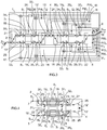
- an amplification device 1 intended for amplifying input optical signals in a Wavelength Division Multiplexing (or WDM) transmission system.
- an amplification device 1 comprises at least a first splitting element 2, first 3 1 and second 3 2 amplification stages, an intermediate processing stage 4, a first combination element 6, and a control means 6.
- the first splitting element 2 is arranged (or configured) for splitting an input optical signal S in in first and second optical signals having respectively first and second polarization modes. As illustrated, this input optical signal S in is provided by a first optical fiber link 7 of a WDM transmission system, which is connected to an input of the amplification device 1.
- the first splitting element 2 may be a polarization beam splitter which may be realized by using a birefringent material that is capable of physically splitting the input optical signal S in in first and second optical signals in order to deliver them respectively onto distant first and second outputs.
- the birefringent material may be a crystal quartz.
- the first polarization mode may be a transverse electric (or TE) mode and the second polarization mode may be a transverse magnetic (or TM) mode.
- TE transverse electric
- TM transverse magnetic
- the reverse situation may be envisaged (i.e. a first polarization mode that is a TM mode and a second polarization mode that is a TE mode) if the amplifier is designed and/or positioned to amplify TM mode.
- TM transverse magnetic
- polarized SOA a SOA arranged for optimally amplifying an optical signal having a predefined polarization mode.
- This type of SOA, optimized for a predefined polarization mode, may be designed to exhibit a very large gain bandwidth.
- the diagram of Figure 2 illustrates an example of evolution of the optical power outputted by a polarized SOA with a very large gain bandwidth as a function of the wavelength in nanometer (nm).
- the gain bandwidth is larger than 120 nm, which represents a threefold increase of optical gain bandwidth with respect to commonly used EDFAs.
- each amplification stage 3 i may be an integrated component that is secured to a small plate (or board) 10 and in two sub-parts of which are respectively defined a first SOA 8 i and a second SOA 9 i .
- the first 3 1 and second 3 2 amplification stages may define a single integrated component 11 that is secured to a small plate (or board) 10 and in four sub-parts of which are respectively defined the two first SOAs 8 i and the two second SOAs 9 i .
- singly polarized SOAs 8 1 and 9 1 in the first amplification stage 3 1 may enable achieving a very large optical bandwidth with high gain, a high output power and a low noise figure.
- the second amplification stage 3 2 one may use singly polarized SOAs 8 2 and 9 2 that enable achieving a very large optical bandwidth with high saturation output power and low gain, so that a large range of output power can be covered while managing the gain flatness.
- the intermediate processing stage 4 is inserted between the first 3 1 and second 3 2 amplification stages. It is arranged for compensating chosen optical characteristics of the optical gain bandwidth of the first amplification stage 3 1 as a function of other driving currents I3 i (or I3) and I4 i (or I4).
- this intermediate processing stage 4 is secured to the small plate (or board) 10.
- the intermediate processing stage 4 comprises a first variable optical attenuator 12 1 , a first gain flattening filter 13 1 , a second variable optical attenuator 12 2 , and a second gain flattening filter 13 2 .
- variable optical attenuators or VOAs
- GFFs gain flattening filters
- the first variable optical attenuator (or VOA) 12 1 is arranged for compensating, on the first optical signal, a tilt of the optical gain bandwidth of the first polarized SOA 8 1 of the first amplification stage 3 1 as a function of a driving current I3 1 .
- the tilt is an example of chosen optical characteristics of the optical gain bandwidth that can be compensated.
- the first gain flattening filter 13 1 is arranged for compensating, on the first optical signal, ripples of the optical gain bandwidth of the first polarized SOA 8 1 of the first amplification stage 3 1 as a function of a driving current I4 1 .
- Ripples are another example of chosen optical characteristics of the optical gain bandwidth that can be compensated.
- the second variable optical attenuator (or VOA) 12 2 is arranged for compensating, on the second optical signal, a tilt of the optical gain bandwidth of the second polarized SOA 9 1 of the first amplification stage 3 1 as a function of a driving current I3 2 .
- the second gain flattening filter 13 2 is arranged for compensating, on the second optical signal, ripples of the optical gain bandwidth of the second polarized SOA 9 1 of the first amplification stage 3 1 as a function of a driving current I4 2 .
- each variable optical attenuator 12 i and each gain flattening filter 13 i are dedicated to the polarization of the modes of the optical signals they receive respectively. This may also allow minimizing polarization dependent gain between the two paths of the amplification device 1.
- each variable optical attenuator 12 i is located upward the associated gain flattening filter 13 i . But this is not mandatory. Indeed, each variable optical attenuator 12 i could be located downward the associated gain flattening filter 13 i .
- the intermediate processing stage 4 comprises a single variable optical attenuator 12', a single gain flattening filter 13', a second combination element 14, and a second splitting element 15.
- the second combination element 14 is arranged for combining the first and second amplified optical signals outputted by the first and second outputs of the first amplification stage 3 1 to produce an intermediate optical signal.
- this second combination element 14 may be a polarization beam combiner, which may be realized by using a birefringent material that is capable of combining the first and second amplified optical signals it receives onto distant first and second inputs in order to deliver an intermediate optical signal.
- the birefringent material may be a crystal quartz.
- variable optical attenuator 12' is arranged for compensating, on this intermediate optical signal, the tilt of the optical gain bandwidth of the first stage 3 1 as a function of a driving current 13.
- the gain flattening filter 13' is arranged for compensating, on the intermediate optical signal, ripples of the first amplification stage 3 1 as a function of a driving current I4.
- variable optical attenuator 12' and the gain flattening filter 13' are not dependent from the polarization.
- variable optical attenuator 12' is located upward the gain flattening filter 13'. But this is not mandatory. Indeed, the variable optical attenuator 12' could be located downward the gain flattening filter 13'.
- the second splitting element 15 is arranged for splitting the intermediate optical signal, processed by the variable optical attenuator 12' and gain flattening filter 13', in the first and second optical signals having respectively the first and second polarization modes.
- this second splitting element 15 may be a polarization beam splitter which may be realized by using a birefringent material that is capable of physically splitting the intermediate optical signal in first and second optical signals in order to deliver them respectively onto distant first and second outputs.
- the birefringent material may be a crystal quartz.
- the first combination element 5 is arranged for combining the first and second amplified optical signals (outputted by the first and second outputs of the second amplification stage 3 2 ) to produce an output optical signal S out . As illustrated, this output optical signal S out feeds a second optical fiber link 16 of the WDM transmission system, which is connected to an output of the amplification device 1.
- the first combination element 5 may be a polarization beam combiner, which may be realized by using a birefringent material that is capable of combining the first and second amplified optical signals it receives onto distant first and second inputs in order to deliver an output optical signal S out .
- the birefringent material may be a crystal quartz.
- first splitting element 2 and the first combination element 5 are secured to the small plate (or board) 10.
- the amplification device 1 preferably comprises further at least a first micro-lens 17 i located just before each first polarized SOA 8 i , a second micro-lens 18 i located just after the first polarized SOA 8 i , a third micro-lens 19 i located just before the second polarized SOA 9 i , and a fourth micro-lens 20 i located just after the second polarized SOA 9 i .
- These micro-lenses 17 i -20 i allow improving light coupling between elements.
- micro-lenses 17 i -20 i are secured to the small plate (or board) 10.
- all the SOAs 8 i and 9 i are defined into the same integrated component 11 and there is no free space between the output of the second combination element 14 and the input of the variable optical attenuator 12' and between the output of the gain flattening filter 13' and the input of the second splitting element 15. So, these two free spaces are replaced with two small optical fiber links 25 and 26. Two other micro-lenses 27 and 28 are also used to allow improving light coupling respectively between the output of the second combination element 14 and the input of the variable optical attenuator 12' and between the output of the gain flattening filter 13' and the input of the second splitting element 15.
- the latter (11) may also comprise thermistor(s).
- the control means 6 is arranged for producing all the driving currents I1 i , I2 i , I3 i (ou I3) et I4 i (ou I4) as a function of information representative of powers of at least the first and second optical signals at least before the first 8 i and second 9 i polarized SOAs and of a targeted power of the output optical signal S out . So, it aims at controlling automatically the respective amplification levels of the first 8 i and second 9 i polarized SOAs of each amplification stage 3 i so that the output optical signal S out be approximately equal to the targeted power (i.e. equal to the latter with a predefined tolerance).
- the control means 6 is preferably made of a combination of hardware and software modules, by means of a microcontroller or a central processing unit (CPU), for instance.
- a microcontroller or a central processing unit (CPU), for instance.
- CPU central processing unit
- the first 8 i and second 9 i polarized SOAs of each amplification stage 3 i are preferably arranged for amplifying optical signals having the first polarization mode (and preferably the TE mode).
- the amplification device 1 must further comprise first 21 and second 22 transformation elements to allow a combination of first and second optical signals with different polarization modes by the first combination element 5, as illustrated in the non-limiting examples of Figures 1 , 3 and 4 .
- the first transformation element 21 is arranged for transforming the second polarization mode of the second optical signal (provided by the second output of the first splitting element 2) in the first polarization mode. So, it is located before the second polarized SOA 9 1 of the first amplification stage 3 1 . It should be understood that this transformation consists in a rotation from the second polarization mode to the first polarization mode.
- the second transformation element 22 is arranged for transforming the first polarization mode of the first optical signal (provided by the output of the first polarized SOA 8 2 of the second amplification stage 3 2 ) in the second polarization mode. So, it is located after the first polarized SOA 8 2 . It should be understood that this transformation consists in a rotation from the first polarization mode to the second polarization mode.
- Such an embodiment allows the first combination element 5 to combine the first optical signal (amplified and having the second polarization mode) with the second optical signal (amplified and having the first polarization mode) to produce the output optical signal S out .
- the first transformation element 21 and/or the second transformation element 22 comprise(s) a waveplate arranged for inducing the above mentioned polarization mode rotations. These waveplates may be used when the above mentioned free spaces are defined.
- the intermediate processing stage 4 must further comprise third 23 and fourth 24 transformation elements.
- the third transformation element 23 is arranged for transforming the first polarization mode of the first optical signal in the second polarization mode before the second combination element 14.
- the fourth transformation element 24 is arranged for transforming the second polarization mode of the second optical signal in the first polarization mode after the second output of the second splitting element 15.
- the third transformation element 23 and/or the fourth transformation element 24 comprise(s) a waveplate arranged for inducing the above mentioned polarization mode rotations. These waveplates may be used when free spaces are defined.
- the amplification device 1 may comprise at least first 29 i and second 30 i extracting elements and first 33 i and second 34 i photodiodes.
- Each first extracting element 29 i is arranged for taking a first predefined percentage of the power of the first optical signal before a corresponding first polarized SOA 8 i .
- Each first photodiode 33 i is arranged for producing a first information PI1 i representative of the power taken from the first optical signal before the corresponding first polarized SOA 8 i for the control means 6.
- Each second extracting element 30 i is arranged for taking a second predefined percentage of the power of the second optical signal before the corresponding second polarized SOA 9 i .
- Each second photodiode 34 i is arranged for producing a second information PI2 i representative of the power taken from the second optical signal before the corresponding second polarized SOA 9 i for the control means 6.
- the first and second predefined percentages may be equal to 1 %. But other values may be used.
- first 29 i and second 30 i extracting elements may each comprise a tap coupler arranged for reflecting the first or second predefined power percentage of the first or second optical signal, and of transmitting the complementary power percentage of the first or second optical signal.
- first or second predefined percentage is equal to 1%
- complementary power percentage is equal to 99%.
- first 29 i and second 30 i extracting elements may be beamsplitters, such as semi-reflective plates or partially reflective mirrors. These beamsplitters may be used when the above mentioned free spaces are defined.
- first 29 i and second 30 i extracting elements are secured to the small plate (or board) 10.
- the first 33 i and second 34 i photodiodes may be secured to the same plate or to a subsidiary plate positioned below the first one.
- first 33 i and second 34 i photodiodes may exhibit a low bandwidth.
- control means 6 may be advantageously arranged for producing all the driving currents I1 i to I4 i as a function also of other information representative of powers of the first and second optical signals after the first 8 i and second 9 i polarized SOAs of ech amplification stage 3 i .
- the amplification device 1 may comprise third 31 i and fourth 32 i extracting elements and third 35 i and fourth 36 i photodiodes.
- Each third extracting element 31 i is arranged for taking a third predefined percentage of the power of the first optical signal after the corresponding first polarized SOA 8 i .
- Each third photodiode 35 i is arranged for producing a third information PI3 i representative of the power taken from the first optical signal after the corresponding first polarized SOA 8 i for the control means 6.
- Each fourth extracting element 32 i is arranged for taking a fourth predefined percentage of the power of the second optical signal after the corresponding second polarized SOA 9 i .
- Each fourth photodiode 36 i is arranged for producing a fourth information PI4 i representative of the power taken from the second optical signal after the corresponding second polarized SOA 9 i for the control means 6.
- the third and fourth predefined percentages may be equal to 1 %. But other values may be used.
- the third 31 i and fourth 32 i extracting elements may each comprise a tap coupler arranged for reflecting the third or fourth predefined power percentage of the first or second amplified optical signal, and of transmitting the complementary power percentage of the first or second amplified optical signal.
- the complementary power percentage is equal to 99%.
- the third 31 i and fourth 32 i extracting elements may be beamsplitters, such as semi-reflective plates or partially reflective mirrors. These beamsplitters may be used when the above mentioned free spaces are defined.
- the third 31 i and fourth 32 i extracting elements are secured to the small plate (or board) 10.
- the third 35 i and fourth 36 i photodiodes may be secured to the same plate or to a subsidiary plate positioned below the first one.
- the third 35 i and fourth 36 i photodiodes may exhibit a low bandwidth.
- the last embodiment allows the control means 6 to precisely balance output powers from the first 8 i and second 9 i SOAs of each amplification stage 3 i according to the targeted power of the output optical signal S out of the amplification device 1. Once this targeted power is set in the control means 6 through the control plane or a manual setting at startup, each optical path should transmit half of this targeted power. So, the control means 6 adjusts all the driving currents I1 i to I4 i accordingly. To this effect, the control means 6 may, for instance, determine the driving currents I1 i to I4 i from stored data establishing a correspondence between information representative of powers and driving currents.
- the control means 6 After having received the power information PI1 i -PI4 i of the two optical paths, the control means 6 finely tunes each driving current I1 i to I4 i to reach the targeted power, while taking into account a tolerance on the targeted power.
- the amplification device 1 may further comprise a polarization dependent optical isolator before each input and/or after each output of each amplification stage 3 i .
- the capacity of a WDM transmission system may be approximately tripled and a management of the gain flatness can be performed.
- the invention also allows to compensate lumped losses in optical networks by means of simple management rules.
Landscapes
- Physics & Mathematics (AREA)
- Electromagnetism (AREA)
- Condensed Matter Physics & Semiconductors (AREA)
- General Physics & Mathematics (AREA)
- Optics & Photonics (AREA)
- Engineering & Computer Science (AREA)
- Computer Networks & Wireless Communication (AREA)
- Signal Processing (AREA)
- Optical Communication System (AREA)
- Lasers (AREA)
- Optical Modulation, Optical Deflection, Nonlinear Optics, Optical Demodulation, Optical Logic Elements (AREA)
Claims (11)
- Dispositif d'amplification (1) comprenant a) un premier élément de séparation (2) agencé pour séparer un signal optique d'entrée en un premier et un deuxième signal optique ayant respectivement un premier et un deuxième mode de polarisation, b) des premier (31) et deuxième (32) étages d'amplification comprenant chacun des premier (8i) et deuxième (9i) amplificateurs optiques à semi-conducteurs polarisés agencés pour amplifier respectivement lesdits premier et deuxième signaux optiques en fonction de courants d'attaque, c) un étage de traitement intermédiaire (4) inséré entre lesdits premier (31) et deuxième (32) étages d'amplification et agencé pour compenser des caractéristiques optiques choisies d'une largeur de bande de gain optique dudit premier étage d'amplification (31) en fonction d'autres courants d'attaque, d) un premier élément de combinaison (5) agencé pour combiner lesdits premier et deuxième signaux optiques amplifiés délivrés par ledit deuxième étage d'amplification (32) pour produire un signal optique de sortie, et e) un moyen de commande (6) agencé pour produire lesdits courants d'attaque en fonction d'informations représentatives de puissances desdits premier et deuxième signaux optiques au moins avant lesdits premier (8i) et deuxième (9i) amplificateurs optiques à semi-conducteurs polarisés de chaque étage d'amplification (3i) et d'une puissance ciblée dudit signal optique de sortie, caractérisé en ce que l'étage de traitement intermédiaire (4) comprend f) un premier atténuateur optique variable (121) agencé pour compenser, sur ledit premier signal optique, une inclinaison de ladite largeur de bande de gain optique dudit premier amplificateur optique à semi-conducteurs polarisé (81) dudit premier étage d'amplification (31), g) un premier filtre d'aplatissement du gain (131) agencé pour compenser, sur ledit premier signal optique, des ondulations de ladite largeur de bande de gain optique dudit premier amplificateur optique à semi-conducteurs polarisé (81) dudit premier étage d'amplification (31), h) un deuxième atténuateur optique variable (122) agencé pour compenser, sur ledit deuxième signal optique, une inclinaison de ladite largeur de bande de gain optique dudit deuxième amplificateur optique à semi-conducteurs polarisé (91) dudit premier étage d'amplification (31), et i) un deuxième filtre d'aplatissement du gain (132) agencé pour compenser, sur ledit deuxième signal optique, des ondulations de ladite largeur de bande de gain optique dudit deuxième amplificateur optique à semi-conducteurs polarisé (91) dudit premier étage d'amplification (31).
- Dispositif d'amplification selon la revendication 1, dans lequel lesdits premier (8i) et deuxième (9i) amplificateurs optiques à semi-conducteurs polarisés de chaque étage d'amplification (3i) sont agencés pour amplifier des signaux optiques ayant ledit premier mode de polarisation, et comprenant en outre un premier élément de transformation (21) agencé pour transformer ledit deuxième mode de polarisation dudit deuxième signal optique en ledit premier mode de polarisation avant ledit deuxième amplificateur optique à semi-conducteurs polarisé (91) dudit premier étage d'amplification (31), et un deuxième élément de transformation (22) agencé pour transformer ledit premier mode de polarisation dudit premier signal optique en ledit deuxième mode de polarisation après ledit premier amplificateur optique à semi-conducteurs polarisé (82) dudit deuxième étage d'amplification (32), de telle sorte que ledit premier élément de combinaison (5) combine ledit premier signal optique amplifié, ayant ledit deuxième mode de polarisation et délivré par ledit deuxième étage d'amplification (32), avec ledit deuxième signal optique amplifié, ayant ledit premier mode de polarisation et délivré par ledit deuxième étage d'amplification (32), pour produire ledit signal optique de sortie.
- Dispositif d'amplification selon la revendication 2, dans lequel ledit premier élément de transformation (21) et/ou ledit deuxième élément de transformation (22) comprend/comprennent une lame à retard.
- Dispositif d'amplification selon une des revendications 1 à 3, comprenant en outre des première (17i) et deuxième (18i) microlentilles respectivement situées juste avant et juste après ledit premier amplificateur optique à semi-conducteurs polarisé (8i) de chaque étage d'amplification (3i), et des troisième (19i) et quatrième (20i) microlentilles respectivement situées juste avant et juste après ledit deuxième amplificateur optique à semi-conducteurs polarisé (9i) de chaque étage d'amplification (3i).
- Dispositif d'amplification selon une des revendications 1 à 4, comprenant en outre, juste avant chaque étage d'amplification (3i), a) un premier élément d'extraction (29i) agencé pour prélever un premier pourcentage prédéfini de la puissance dudit premier signal optique avant ledit premier amplificateur optique à semi-conducteurs polarisé (8i), b) une première photodiode (33i) agencée pour produire une première information représentative de la puissance prélevée à partir dudit premier signal optique avant ledit premier amplificateur optique à semi-conducteurs polarisé (8i) pour ledit moyen de commande (6), c) un deuxième élément d'extraction (30i) agencé pour prélever un deuxième pourcentage prédéfini de la puissance dudit deuxième signal optique avant ledit deuxième amplificateur optique à semi-conducteurs polarisé (9i), et d) une deuxième photodiode (34i) agencée pour produire une deuxième information représentative de la puissance prélevée à partir dudit deuxième signal optique avant ledit deuxième amplificateur optique à semi-conducteurs polarisé (9i) pour ledit moyen de commande (6).
- Dispositif d'amplification selon une des revendications 1 à 5, dans lequel ledit moyen de commande (6) est agencé pour produire lesdits courants d'attaque en fonction d'informations représentatives de puissances desdits premier et deuxième signaux optiques avant et après lesdits premier (8i) et deuxième (9i) amplificateurs optiques à semi-conducteurs polarisés de chaque étage d'amplification (3i) et de ladite puissance ciblée dudit signal optique de sortie.
- Dispositif d'amplification selon la revendication 6, comprenant en outre, après chaque étage d'amplification (3i), a) un troisième élément d'extraction (31i) agencé pour prélever un troisième pourcentage prédéfini de la puissance dudit premier signal optique après ledit premier amplificateur optique à semi-conducteurs polarisé (8i), b) une troisième photodiode (35i) agencée pour produire une troisième information représentative de la puissance prélevée à partir dudit premier signal optique après ledit premier amplificateur optique à semi-conducteurs polarisé (8i) pour ledit moyen de commande (6), c) un quatrième élément d'extraction (32i) agencé pour prélever un quatrième pourcentage prédéfini de la puissance dudit deuxième signal optique après ledit deuxième amplificateur optique à semi-conducteurs polarisé (9i), et d) une quatrième photodiode (36i) agencée pour produire une quatrième information représentative de la puissance prélevée à partir dudit deuxième signal optique après ledit deuxième amplificateur optique à semi-conducteurs polarisé (9i) pour ledit moyen de commande (6) .
- Dispositif d'amplification selon une des revendications 1 à 7, dans lequel ledit premier mode de polarisation est un mode électrique transverse et ledit deuxième mode de polarisation est un mode magnétique transverse.
- Dispositif d'amplification selon une des revendications 1 à 8, dans lequel chaque élément de séparation (2 ; 15) et/ou chaque élément de combinaison (5 ; 14) comprend/comprennent un matériau biréfringent.
- Dispositif d'amplification selon une des revendications 1 à 9, dans lequel ledit moyen de commande (6) est agencé pour déterminer lesdits courants d'attaque à partir de données stockées établissant une correspondance entre des informations représentatives de puissances et des courants d'attaque.
- Dispositif d'amplification selon une des revendications 1 à 10, comprenant en outre un isolateur optique dépendant de la polarisation avant chaque entrée et/ou après chaque sortie de chaque étage d'amplification (3i).
Priority Applications (5)
| Application Number | Priority Date | Filing Date | Title |
|---|---|---|---|
| EP15306493.6A EP3148100B1 (fr) | 2015-09-25 | 2015-09-25 | Dispositif d'amplification avec des étages d'amplification doté d'un étage de traitement et de soas polarisées permettant d'amplifier des signaux optiques dans un système de transmission wdm |
| CN201680065274.6A CN108352902A (zh) | 2015-09-25 | 2016-09-23 | 用于放大wdm发射系统中的光信号的具有具经偏振soa的放大级和处理级的放大装置 |
| PCT/EP2016/072773 WO2017051018A1 (fr) | 2015-09-25 | 2016-09-23 | Dispositif d'amplification à étages d'amplification à amplificateurs optiques à semi-conducteurs polarisés et à étage de traitement, servant à amplifier des signaux optiques dans un système de transmission par multiplexage en longueur d'onde |
| EP16770762.9A EP3353909B1 (fr) | 2015-09-25 | 2016-09-23 | Dispositif d'amplification avec des étages d'amplification doté d'un étage de traitement et de soas polarisées permettant d'amplifier des signaux optiques dans un système de transmission wdm |
| US15/934,122 US10419149B2 (en) | 2015-09-25 | 2018-03-23 | Amplification device with amplification stages with polarized SOAs and processing stage, for amplifying optical signals in a WDM transmission system |
Applications Claiming Priority (1)
| Application Number | Priority Date | Filing Date | Title |
|---|---|---|---|
| EP15306493.6A EP3148100B1 (fr) | 2015-09-25 | 2015-09-25 | Dispositif d'amplification avec des étages d'amplification doté d'un étage de traitement et de soas polarisées permettant d'amplifier des signaux optiques dans un système de transmission wdm |
Publications (2)
| Publication Number | Publication Date |
|---|---|
| EP3148100A1 EP3148100A1 (fr) | 2017-03-29 |
| EP3148100B1 true EP3148100B1 (fr) | 2019-03-13 |
Family
ID=54292752
Family Applications (2)
| Application Number | Title | Priority Date | Filing Date |
|---|---|---|---|
| EP15306493.6A Not-in-force EP3148100B1 (fr) | 2015-09-25 | 2015-09-25 | Dispositif d'amplification avec des étages d'amplification doté d'un étage de traitement et de soas polarisées permettant d'amplifier des signaux optiques dans un système de transmission wdm |
| EP16770762.9A Active EP3353909B1 (fr) | 2015-09-25 | 2016-09-23 | Dispositif d'amplification avec des étages d'amplification doté d'un étage de traitement et de soas polarisées permettant d'amplifier des signaux optiques dans un système de transmission wdm |
Family Applications After (1)
| Application Number | Title | Priority Date | Filing Date |
|---|---|---|---|
| EP16770762.9A Active EP3353909B1 (fr) | 2015-09-25 | 2016-09-23 | Dispositif d'amplification avec des étages d'amplification doté d'un étage de traitement et de soas polarisées permettant d'amplifier des signaux optiques dans un système de transmission wdm |
Country Status (4)
| Country | Link |
|---|---|
| US (1) | US10419149B2 (fr) |
| EP (2) | EP3148100B1 (fr) |
| CN (1) | CN108352902A (fr) |
| WO (1) | WO2017051018A1 (fr) |
Families Citing this family (5)
| Publication number | Priority date | Publication date | Assignee | Title |
|---|---|---|---|---|
| JP6968359B2 (ja) * | 2017-08-08 | 2021-11-17 | 富士通株式会社 | 光増幅器及び光スイッチ装置 |
| WO2022135701A1 (fr) * | 2020-12-22 | 2022-06-30 | Huawei Technologies Co., Ltd. | Module amplificateur optique à faible atténuation liée à la polarisation |
| CN115021822B (zh) * | 2022-05-12 | 2023-09-12 | 昂纳科技(深圳)集团股份有限公司 | 一种光传输系统 |
| WO2024041718A1 (fr) * | 2022-08-22 | 2024-02-29 | Huawei Cloud Computing Technologies Co., Ltd. | Unité d'amplificateur optique et étage d'amplificateur optique |
| WO2026012589A1 (fr) * | 2024-07-10 | 2026-01-15 | Huawei Technologies Co., Ltd. | Agencement pour atténuer le bruit non linéaire d'amplificateurs optiques à semi-conducteurs en cascade |
Family Cites Families (11)
| Publication number | Priority date | Publication date | Assignee | Title |
|---|---|---|---|---|
| DE3885389T2 (de) * | 1987-09-01 | 1994-03-24 | Nippon Electric Co | Optischer Zwischenverstärker. |
| JP3854673B2 (ja) * | 1996-11-25 | 2006-12-06 | 株式会社日立コミュニケーションテクノロジー | 光増幅媒体制御方法及び光増幅装置並びにそれを利用したシステム |
| US6560010B1 (en) * | 2000-12-14 | 2003-05-06 | Genoa Corporation | Broadband gain-clamped semiconductor optical amplifier devices |
| EP1261086A1 (fr) * | 2001-05-25 | 2002-11-27 | Corning Incorporated | Amplificateur à semi-conducteur à gain élevé, puissance élevée et à faible bruit |
| US6809863B2 (en) * | 2001-06-07 | 2004-10-26 | Cirvine Corporation | Low dispersion filters |
| GB0413017D0 (en) * | 2004-06-10 | 2004-07-14 | Bookham Technology Plc | Optical amplifiers |
| US9020366B2 (en) * | 2011-01-24 | 2015-04-28 | Nec Corporation | Polarization multiplexing optical receiving device and polarization multiplexing optical receiving method |
| CN102231035B (zh) * | 2011-05-30 | 2013-05-22 | 武汉邮电科学研究院 | 双半导体光放大器结构的全光波长转换器及转换方法 |
| JP2013058628A (ja) * | 2011-09-08 | 2013-03-28 | Furukawa Electric Co Ltd:The | 光増幅装置 |
| US8964284B2 (en) * | 2012-04-18 | 2015-02-24 | Infinera Corporation | Banded semiconductor optical amplifier |
| JP6244672B2 (ja) * | 2013-06-04 | 2017-12-13 | 富士通オプティカルコンポーネンツ株式会社 | 光源モジュール、および光送受信装置 |
-
2015
- 2015-09-25 EP EP15306493.6A patent/EP3148100B1/fr not_active Not-in-force
-
2016
- 2016-09-23 EP EP16770762.9A patent/EP3353909B1/fr active Active
- 2016-09-23 CN CN201680065274.6A patent/CN108352902A/zh active Pending
- 2016-09-23 WO PCT/EP2016/072773 patent/WO2017051018A1/fr not_active Ceased
-
2018
- 2018-03-23 US US15/934,122 patent/US10419149B2/en not_active Expired - Fee Related
Non-Patent Citations (1)
| Title |
|---|
| None * |
Also Published As
| Publication number | Publication date |
|---|---|
| EP3353909A1 (fr) | 2018-08-01 |
| US20180212702A1 (en) | 2018-07-26 |
| CN108352902A (zh) | 2018-07-31 |
| WO2017051018A1 (fr) | 2017-03-30 |
| EP3353909B1 (fr) | 2019-11-13 |
| EP3148100A1 (fr) | 2017-03-29 |
| US10419149B2 (en) | 2019-09-17 |
Similar Documents
| Publication | Publication Date | Title |
|---|---|---|
| US10419149B2 (en) | Amplification device with amplification stages with polarized SOAs and processing stage, for amplifying optical signals in a WDM transmission system | |
| US9699531B2 (en) | Switchable optical amplifier and optical transmission apparatus | |
| JP3638777B2 (ja) | 利得等化のための方法並びに該方法の実施に使用する装置及びシステム | |
| Inoue et al. | Tunable gain equalization using a Mach-Zehnder optical filter in multistage fiber amplifiers | |
| US8666252B2 (en) | Optical network system | |
| CN111698033B (zh) | 混合光纤放大器、光信号放大方法及光通信系统 | |
| JP6608747B2 (ja) | 波長多重光受信装置及びその駆動方法 | |
| US8670176B2 (en) | Optical amplifying device | |
| US6657774B1 (en) | Amplifier system with distributed and discrete Raman fiber amplifiers | |
| EP3510709B1 (fr) | Systèmes de communication optique multiplexés par répartition spatiale et amplificateurs associés | |
| JPH09191303A (ja) | 光伝送路 | |
| WO2017008073A1 (fr) | Amélioration du rapport signal-bruit optique d'un émetteur par amplification d'un récepteur dans les systèmes cohérents à laser unique | |
| US11296810B2 (en) | Add drop structure | |
| US20190052056A1 (en) | Optical module and method for controlling optical module | |
| JP2006066862A (ja) | 波長多重信号光の増幅方法および光増幅器 | |
| US20080080805A1 (en) | Compensating method and compensator of first-order polarization mode dispersion, and optical transmission system using same | |
| JP2001203644A (ja) | 光増幅器および光増幅方法 | |
| US20030081285A1 (en) | Transmission device having wavelength-band-specific optical amplifiers provided commonly for all transmission lines | |
| EP3148018A1 (fr) | Dispositif d'amplification à soa polarisée, permettant d'amplifier des signaux optiques dans un système de transmission wdm | |
| JPWO2018207835A1 (ja) | 光中継器、光中継器の制御方法、及び光伝送システム | |
| US8681420B2 (en) | Optical transmission system | |
| US7027215B2 (en) | Optical component, optical amplification module, and optical transmission system | |
| JP2012043934A (ja) | 増幅装置、通信システムおよび増幅方法 | |
| EP1128581A1 (fr) | Amplificateur optique avec égalisateur de gain | |
| JP5967737B1 (ja) | 光通信システム及びマルチモード光ファイバ増幅装置 |
Legal Events
| Date | Code | Title | Description |
|---|---|---|---|
| PUAI | Public reference made under article 153(3) epc to a published international application that has entered the european phase |
Free format text: ORIGINAL CODE: 0009012 |
|
| STAA | Information on the status of an ep patent application or granted ep patent |
Free format text: STATUS: THE APPLICATION HAS BEEN PUBLISHED |
|
| AK | Designated contracting states |
Kind code of ref document: A1 Designated state(s): AL AT BE BG CH CY CZ DE DK EE ES FI FR GB GR HR HU IE IS IT LI LT LU LV MC MK MT NL NO PL PT RO RS SE SI SK SM TR |
|
| AX | Request for extension of the european patent |
Extension state: BA ME |
|
| STAA | Information on the status of an ep patent application or granted ep patent |
Free format text: STATUS: REQUEST FOR EXAMINATION WAS MADE |
|
| 17P | Request for examination filed |
Effective date: 20170926 |
|
| RBV | Designated contracting states (corrected) |
Designated state(s): AL AT BE BG CH CY CZ DE DK EE ES FI FR GB GR HR HU IE IS IT LI LT LU LV MC MK MT NL NO PL PT RO RS SE SI SK SM TR |
|
| GRAP | Despatch of communication of intention to grant a patent |
Free format text: ORIGINAL CODE: EPIDOSNIGR1 |
|
| RAP1 | Party data changed (applicant data changed or rights of an application transferred) |
Owner name: ALCATEL LUCENT |
|
| STAA | Information on the status of an ep patent application or granted ep patent |
Free format text: STATUS: GRANT OF PATENT IS INTENDED |
|
| INTG | Intention to grant announced |
Effective date: 20180419 |
|
| GRAS | Grant fee paid |
Free format text: ORIGINAL CODE: EPIDOSNIGR3 |
|
| GRAJ | Information related to disapproval of communication of intention to grant by the applicant or resumption of examination proceedings by the epo deleted |
Free format text: ORIGINAL CODE: EPIDOSDIGR1 |
|
| GRAL | Information related to payment of fee for publishing/printing deleted |
Free format text: ORIGINAL CODE: EPIDOSDIGR3 |
|
| STAA | Information on the status of an ep patent application or granted ep patent |
Free format text: STATUS: REQUEST FOR EXAMINATION WAS MADE |
|
| GRAP | Despatch of communication of intention to grant a patent |
Free format text: ORIGINAL CODE: EPIDOSNIGR1 |
|
| INTC | Intention to grant announced (deleted) | ||
| STAA | Information on the status of an ep patent application or granted ep patent |
Free format text: STATUS: GRANT OF PATENT IS INTENDED |
|
| INTG | Intention to grant announced |
Effective date: 20181004 |
|
| RIN1 | Information on inventor provided before grant (corrected) |
Inventor name: BRENOT, ROMAIN Inventor name: RENAUDIER, JEREMIE Inventor name: CHARLET, GABRIEL |
|
| GRAA | (expected) grant |
Free format text: ORIGINAL CODE: 0009210 |
|
| STAA | Information on the status of an ep patent application or granted ep patent |
Free format text: STATUS: THE PATENT HAS BEEN GRANTED |
|
| AK | Designated contracting states |
Kind code of ref document: B1 Designated state(s): AL AT BE BG CH CY CZ DE DK EE ES FI FR GB GR HR HU IE IS IT LI LT LU LV MC MK MT NL NO PL PT RO RS SE SI SK SM TR |
|
| REG | Reference to a national code |
Ref country code: GB Ref legal event code: FG4D |
|
| REG | Reference to a national code |
Ref country code: CH Ref legal event code: EP Ref country code: AT Ref legal event code: REF Ref document number: 1109116 Country of ref document: AT Kind code of ref document: T Effective date: 20190315 |
|
| REG | Reference to a national code |
Ref country code: IE Ref legal event code: FG4D |
|
| REG | Reference to a national code |
Ref country code: DE Ref legal event code: R096 Ref document number: 602015026260 Country of ref document: DE |
|
| REG | Reference to a national code |
Ref country code: NL Ref legal event code: MP Effective date: 20190313 |
|
| REG | Reference to a national code |
Ref country code: LT Ref legal event code: MG4D |
|
| PG25 | Lapsed in a contracting state [announced via postgrant information from national office to epo] |
Ref country code: FI Free format text: LAPSE BECAUSE OF FAILURE TO SUBMIT A TRANSLATION OF THE DESCRIPTION OR TO PAY THE FEE WITHIN THE PRESCRIBED TIME-LIMIT Effective date: 20190313 Ref country code: SE Free format text: LAPSE BECAUSE OF FAILURE TO SUBMIT A TRANSLATION OF THE DESCRIPTION OR TO PAY THE FEE WITHIN THE PRESCRIBED TIME-LIMIT Effective date: 20190313 Ref country code: NO Free format text: LAPSE BECAUSE OF FAILURE TO SUBMIT A TRANSLATION OF THE DESCRIPTION OR TO PAY THE FEE WITHIN THE PRESCRIBED TIME-LIMIT Effective date: 20190613 Ref country code: LT Free format text: LAPSE BECAUSE OF FAILURE TO SUBMIT A TRANSLATION OF THE DESCRIPTION OR TO PAY THE FEE WITHIN THE PRESCRIBED TIME-LIMIT Effective date: 20190313 |
|
| PG25 | Lapsed in a contracting state [announced via postgrant information from national office to epo] |
Ref country code: GR Free format text: LAPSE BECAUSE OF FAILURE TO SUBMIT A TRANSLATION OF THE DESCRIPTION OR TO PAY THE FEE WITHIN THE PRESCRIBED TIME-LIMIT Effective date: 20190614 Ref country code: HR Free format text: LAPSE BECAUSE OF FAILURE TO SUBMIT A TRANSLATION OF THE DESCRIPTION OR TO PAY THE FEE WITHIN THE PRESCRIBED TIME-LIMIT Effective date: 20190313 Ref country code: BG Free format text: LAPSE BECAUSE OF FAILURE TO SUBMIT A TRANSLATION OF THE DESCRIPTION OR TO PAY THE FEE WITHIN THE PRESCRIBED TIME-LIMIT Effective date: 20190613 Ref country code: RS Free format text: LAPSE BECAUSE OF FAILURE TO SUBMIT A TRANSLATION OF THE DESCRIPTION OR TO PAY THE FEE WITHIN THE PRESCRIBED TIME-LIMIT Effective date: 20190313 Ref country code: NL Free format text: LAPSE BECAUSE OF FAILURE TO SUBMIT A TRANSLATION OF THE DESCRIPTION OR TO PAY THE FEE WITHIN THE PRESCRIBED TIME-LIMIT Effective date: 20190313 Ref country code: LV Free format text: LAPSE BECAUSE OF FAILURE TO SUBMIT A TRANSLATION OF THE DESCRIPTION OR TO PAY THE FEE WITHIN THE PRESCRIBED TIME-LIMIT Effective date: 20190313 |
|
| REG | Reference to a national code |
Ref country code: AT Ref legal event code: MK05 Ref document number: 1109116 Country of ref document: AT Kind code of ref document: T Effective date: 20190313 |
|
| PG25 | Lapsed in a contracting state [announced via postgrant information from national office to epo] |
Ref country code: RO Free format text: LAPSE BECAUSE OF FAILURE TO SUBMIT A TRANSLATION OF THE DESCRIPTION OR TO PAY THE FEE WITHIN THE PRESCRIBED TIME-LIMIT Effective date: 20190313 Ref country code: SK Free format text: LAPSE BECAUSE OF FAILURE TO SUBMIT A TRANSLATION OF THE DESCRIPTION OR TO PAY THE FEE WITHIN THE PRESCRIBED TIME-LIMIT Effective date: 20190313 Ref country code: EE Free format text: LAPSE BECAUSE OF FAILURE TO SUBMIT A TRANSLATION OF THE DESCRIPTION OR TO PAY THE FEE WITHIN THE PRESCRIBED TIME-LIMIT Effective date: 20190313 Ref country code: IT Free format text: LAPSE BECAUSE OF FAILURE TO SUBMIT A TRANSLATION OF THE DESCRIPTION OR TO PAY THE FEE WITHIN THE PRESCRIBED TIME-LIMIT Effective date: 20190313 Ref country code: ES Free format text: LAPSE BECAUSE OF FAILURE TO SUBMIT A TRANSLATION OF THE DESCRIPTION OR TO PAY THE FEE WITHIN THE PRESCRIBED TIME-LIMIT Effective date: 20190313 Ref country code: AL Free format text: LAPSE BECAUSE OF FAILURE TO SUBMIT A TRANSLATION OF THE DESCRIPTION OR TO PAY THE FEE WITHIN THE PRESCRIBED TIME-LIMIT Effective date: 20190313 Ref country code: PT Free format text: LAPSE BECAUSE OF FAILURE TO SUBMIT A TRANSLATION OF THE DESCRIPTION OR TO PAY THE FEE WITHIN THE PRESCRIBED TIME-LIMIT Effective date: 20190713 Ref country code: CZ Free format text: LAPSE BECAUSE OF FAILURE TO SUBMIT A TRANSLATION OF THE DESCRIPTION OR TO PAY THE FEE WITHIN THE PRESCRIBED TIME-LIMIT Effective date: 20190313 |
|
| PG25 | Lapsed in a contracting state [announced via postgrant information from national office to epo] |
Ref country code: PL Free format text: LAPSE BECAUSE OF FAILURE TO SUBMIT A TRANSLATION OF THE DESCRIPTION OR TO PAY THE FEE WITHIN THE PRESCRIBED TIME-LIMIT Effective date: 20190313 Ref country code: SM Free format text: LAPSE BECAUSE OF FAILURE TO SUBMIT A TRANSLATION OF THE DESCRIPTION OR TO PAY THE FEE WITHIN THE PRESCRIBED TIME-LIMIT Effective date: 20190313 |
|
| REG | Reference to a national code |
Ref country code: DE Ref legal event code: R097 Ref document number: 602015026260 Country of ref document: DE |
|
| PG25 | Lapsed in a contracting state [announced via postgrant information from national office to epo] |
Ref country code: AT Free format text: LAPSE BECAUSE OF FAILURE TO SUBMIT A TRANSLATION OF THE DESCRIPTION OR TO PAY THE FEE WITHIN THE PRESCRIBED TIME-LIMIT Effective date: 20190313 Ref country code: IS Free format text: LAPSE BECAUSE OF FAILURE TO SUBMIT A TRANSLATION OF THE DESCRIPTION OR TO PAY THE FEE WITHIN THE PRESCRIBED TIME-LIMIT Effective date: 20190713 |
|
| PLBE | No opposition filed within time limit |
Free format text: ORIGINAL CODE: 0009261 |
|
| STAA | Information on the status of an ep patent application or granted ep patent |
Free format text: STATUS: NO OPPOSITION FILED WITHIN TIME LIMIT |
|
| PG25 | Lapsed in a contracting state [announced via postgrant information from national office to epo] |
Ref country code: DK Free format text: LAPSE BECAUSE OF FAILURE TO SUBMIT A TRANSLATION OF THE DESCRIPTION OR TO PAY THE FEE WITHIN THE PRESCRIBED TIME-LIMIT Effective date: 20190313 |
|
| 26N | No opposition filed |
Effective date: 20191216 |
|
| PG25 | Lapsed in a contracting state [announced via postgrant information from national office to epo] |
Ref country code: SI Free format text: LAPSE BECAUSE OF FAILURE TO SUBMIT A TRANSLATION OF THE DESCRIPTION OR TO PAY THE FEE WITHIN THE PRESCRIBED TIME-LIMIT Effective date: 20190313 |
|
| PG25 | Lapsed in a contracting state [announced via postgrant information from national office to epo] |
Ref country code: TR Free format text: LAPSE BECAUSE OF FAILURE TO SUBMIT A TRANSLATION OF THE DESCRIPTION OR TO PAY THE FEE WITHIN THE PRESCRIBED TIME-LIMIT Effective date: 20190313 |
|
| REG | Reference to a national code |
Ref country code: DE Ref legal event code: R119 Ref document number: 602015026260 Country of ref document: DE |
|
| PG25 | Lapsed in a contracting state [announced via postgrant information from national office to epo] |
Ref country code: MC Free format text: LAPSE BECAUSE OF FAILURE TO SUBMIT A TRANSLATION OF THE DESCRIPTION OR TO PAY THE FEE WITHIN THE PRESCRIBED TIME-LIMIT Effective date: 20190313 |
|
| REG | Reference to a national code |
Ref country code: CH Ref legal event code: PL |
|
| PG25 | Lapsed in a contracting state [announced via postgrant information from national office to epo] |
Ref country code: DE Free format text: LAPSE BECAUSE OF NON-PAYMENT OF DUE FEES Effective date: 20200401 Ref country code: LU Free format text: LAPSE BECAUSE OF NON-PAYMENT OF DUE FEES Effective date: 20190925 Ref country code: LI Free format text: LAPSE BECAUSE OF NON-PAYMENT OF DUE FEES Effective date: 20190930 Ref country code: IE Free format text: LAPSE BECAUSE OF NON-PAYMENT OF DUE FEES Effective date: 20190925 Ref country code: CH Free format text: LAPSE BECAUSE OF NON-PAYMENT OF DUE FEES Effective date: 20190930 |
|
| REG | Reference to a national code |
Ref country code: BE Ref legal event code: MM Effective date: 20190930 |
|
| PG25 | Lapsed in a contracting state [announced via postgrant information from national office to epo] |
Ref country code: BE Free format text: LAPSE BECAUSE OF NON-PAYMENT OF DUE FEES Effective date: 20190930 |
|
| GBPC | Gb: european patent ceased through non-payment of renewal fee |
Effective date: 20190925 |
|
| PG25 | Lapsed in a contracting state [announced via postgrant information from national office to epo] |
Ref country code: GB Free format text: LAPSE BECAUSE OF NON-PAYMENT OF DUE FEES Effective date: 20190925 Ref country code: FR Free format text: LAPSE BECAUSE OF NON-PAYMENT OF DUE FEES Effective date: 20190930 |
|
| PG25 | Lapsed in a contracting state [announced via postgrant information from national office to epo] |
Ref country code: CY Free format text: LAPSE BECAUSE OF FAILURE TO SUBMIT A TRANSLATION OF THE DESCRIPTION OR TO PAY THE FEE WITHIN THE PRESCRIBED TIME-LIMIT Effective date: 20190313 |
|
| PG25 | Lapsed in a contracting state [announced via postgrant information from national office to epo] |
Ref country code: MT Free format text: LAPSE BECAUSE OF FAILURE TO SUBMIT A TRANSLATION OF THE DESCRIPTION OR TO PAY THE FEE WITHIN THE PRESCRIBED TIME-LIMIT Effective date: 20190313 Ref country code: HU Free format text: LAPSE BECAUSE OF FAILURE TO SUBMIT A TRANSLATION OF THE DESCRIPTION OR TO PAY THE FEE WITHIN THE PRESCRIBED TIME-LIMIT; INVALID AB INITIO Effective date: 20150925 |
|
| PG25 | Lapsed in a contracting state [announced via postgrant information from national office to epo] |
Ref country code: MK Free format text: LAPSE BECAUSE OF FAILURE TO SUBMIT A TRANSLATION OF THE DESCRIPTION OR TO PAY THE FEE WITHIN THE PRESCRIBED TIME-LIMIT Effective date: 20190313 |