EP3150977B1 - Thermischer durchflussmesser - Google Patents
Thermischer durchflussmesser Download PDFInfo
- Publication number
- EP3150977B1 EP3150977B1 EP15798963.3A EP15798963A EP3150977B1 EP 3150977 B1 EP3150977 B1 EP 3150977B1 EP 15798963 A EP15798963 A EP 15798963A EP 3150977 B1 EP3150977 B1 EP 3150977B1
- Authority
- EP
- European Patent Office
- Prior art keywords
- signal
- circuit
- switching
- vfo
- switching element
- Prior art date
- Legal status (The legal status is an assumption and is not a legal conclusion. Google has not performed a legal analysis and makes no representation as to the accuracy of the status listed.)
- Not-in-force
Links
Images






Classifications
-
- G—PHYSICS
- G01—MEASURING; TESTING
- G01F—MEASURING VOLUME, VOLUME FLOW, MASS FLOW OR LIQUID LEVEL; METERING BY VOLUME
- G01F1/00—Measuring the volume flow or mass flow of fluid or fluent solid material wherein the fluid passes through a meter in a continuous flow
- G01F1/68—Measuring the volume flow or mass flow of fluid or fluent solid material wherein the fluid passes through a meter in a continuous flow by using thermal effects
- G01F1/696—Circuits therefor, e.g. constant-current flow meters
- G01F1/698—Feedback or rebalancing circuits, e.g. self heated constant temperature flowmeters
-
- H—ELECTRICITY
- H03—ELECTRONIC CIRCUITRY
- H03K—PULSE TECHNIQUE
- H03K4/00—Generating pulses having essentially a finite slope or stepped portions
- H03K4/94—Generating pulses having essentially a finite slope or stepped portions having trapezoidal shape
-
- H—ELECTRICITY
- H03—ELECTRONIC CIRCUITRY
- H03K—PULSE TECHNIQUE
- H03K17/00—Electronic switching or gating, i.e. not by contact-making and –breaking
- H03K17/16—Modifications for eliminating interference voltages or currents
-
- H—ELECTRICITY
- H03—ELECTRONIC CIRCUITRY
- H03K—PULSE TECHNIQUE
- H03K17/00—Electronic switching or gating, i.e. not by contact-making and –breaking
- H03K17/16—Modifications for eliminating interference voltages or currents
- H03K17/161—Modifications for eliminating interference voltages or currents in field-effect transistor switches
- H03K17/162—Modifications for eliminating interference voltages or currents in field-effect transistor switches without feedback from the output circuit to the control circuit
-
- H—ELECTRICITY
- H03—ELECTRONIC CIRCUITRY
- H03K—PULSE TECHNIQUE
- H03K17/00—Electronic switching or gating, i.e. not by contact-making and –breaking
- H03K17/16—Modifications for eliminating interference voltages or currents
- H03K17/161—Modifications for eliminating interference voltages or currents in field-effect transistor switches
- H03K17/162—Modifications for eliminating interference voltages or currents in field-effect transistor switches without feedback from the output circuit to the control circuit
- H03K17/163—Soft switching
- H03K17/164—Soft switching using parallel switching arrangements
-
- H—ELECTRICITY
- H03—ELECTRONIC CIRCUITRY
- H03K—PULSE TECHNIQUE
- H03K17/00—Electronic switching or gating, i.e. not by contact-making and –breaking
- H03K17/28—Modifications for introducing a time delay before switching
- H03K17/284—Modifications for introducing a time delay before switching in field effect transistor switches
-
- H—ELECTRICITY
- H03—ELECTRONIC CIRCUITRY
- H03K—PULSE TECHNIQUE
- H03K19/00—Logic circuits, i.e. having at least two inputs acting on one output; Inverting circuits
- H03K19/0175—Coupling arrangements; Interface arrangements
-
- H—ELECTRICITY
- H03—ELECTRONIC CIRCUITRY
- H03K—PULSE TECHNIQUE
- H03K4/00—Generating pulses having essentially a finite slope or stepped portions
- H03K4/06—Generating pulses having essentially a finite slope or stepped portions having triangular shape
Definitions
- the present invention relates to a thermal-type flow meter.
- a thermal-type flow meter is a sensor to measure a flow rate of flown air on the basis of a current necessary for returning a temperature of a heating wire which is changed by the ambient flowing air.
- the measured flow rate can be represented by a periodic signal having a frequency corresponding to the flow rate for example.
- the periodic signal is input to an open drain circuit (or an open collector circuit; the same shall apply hereinafter) for example, and a frequency of a signal output from the open drain circuit is detected by a frequency measurement circuit, so that the flow rate can be detected.
- the open drain circuit turns on/off a switching element to output an output signal of a high/low level.
- the output signal corresponding to the flow rate represented by the frequency of the periodic signal can be output by turning on/off the switching element according to the frequency of the periodic signal.
- the output signal becomes a rectangular wave due to the configuration of the open drain circuit. Therefore, high-frequency noises are generated.
- a plurality of switching elements are connected in parallel at multiple stages, and shifts timing for switching the switching elements so as to output the step-shape output signal.
- PTL 1 describes a specific example of the open drain circuit in which the switching timings of the respective switching elements are different.
- An air flow meter is for example also described in EP 0628715 A2 .
- an amplification circuit is generally disclosed in EP 2063531 A .
- a frequency of a periodic signal input to an open drain circuit changes according to a measured flow rate. Therefore, the ON/OFF period of the switching element of the open drain circuit is shortened when the frequency of the periodic signal is increased.
- a delay time interval between the switching elements is constant. Therefore, when the frequency of the periodic signal is increased to some degree or more, the switching element at the first stage makes an operation of the next period before the switching element at the final stage operates. Therefore, there is a possibility that the output signal may be not changed from the high level to the low level in one period. In this case, it is difficult to detect a flow rate represented by the frequency of the periodic signal with accuracy.
- the invention has been made in view of the problems described above, and an object thereof is to provide a thermal-type flow meter which measures a flow rate of air using the frequency of the periodic signal, in which a waveform abnormality of the output signal caused by a frequency change can be avoided while suppressing high-frequency noises.
- a thermal-type flow meter includes a plurality of switching elements connected in parallel, and changes a delay duration between the switching elements according to a frequency change of the periodic signal representing a flow rate.
- thermo-type flow meter of the invention it is possible to suppress that a peak value and a frequency of an output signal become abnormal values even when the frequency of the periodic signal changes while suppressing high-frequency noises caused from a plurality of switching elements connected in parallel.
- Countermeasures for radiation electromagnetic waves generated when an output signal indicating information using a frequency is output from an open collector circuit are as follows.
- FIG. 1 is an exemplary waveform of the output signal in a case where an electromagnetic wave noise is suppressed using a low-pass filter.
- the low-pass filter configured by a combination of an inductor, a capacitor, and a resistor is disposed in an output terminal of an open drain circuit.
- a voltage is steeply changed at the beginning when the output signal falls down and rises up, and a high-frequency component is contained in the output signal.
- the waveform when the voltage V falls down is expressed by the following Equation 1, and the waveform when the voltage V rises up is expressed by the following Equation 2.
- A is a peak value
- ⁇ is a time constant
- ⁇ is a constant
- t time.
- V A ⁇ Exp ⁇ ⁇ ⁇ t + ⁇
- V A ⁇ 1 ⁇ Exp ⁇ ⁇ ⁇ t + ⁇
- FIG. 2 is a diagram illustrating an exemplary waveform of the output signal in a case where a current flowing to the open drain circuit is limited using a current mirror circuit. In this case, the current is not limited when the voltage falls down as illustrated in FIG. 2 .
- An ideal waveform as a periodic signal is a sinusoidal waveform.
- a transistor of the output stage is turned ON/OFF, and the voltage of the output signal is received from an external voltage source. Therefore, a signal waveform output by the open drain circuit becomes a rectangular waveform as a principle.
- Equation 3 represents a waveform of the current flowing into the output terminal of the open drain circuit.
- a magnetic field H is generated around the current I as expressed in Equation 4.
- r represents a distance from the current.
- Equation 5 A relation between the magnetic field H and the electric field E is expressed by the following Equation 5 using Maxwell's equations.
- ⁇ magnetic permeability
- a small temporal variation of the current flowing to the output terminal of the open drain circuit is an effective countermeasure against the high-frequency noise from Equations 4 and 5.
- a method of realizing the countermeasure there is considered a method in which a plurality of open drain transistors are connected to the output terminal in parallel, a time difference is put at a switching timing of conducting the transistor, and the current flowing to the output terminal is switched in plural times.
- FIG. 3 is a circuit diagram illustrating an example of the open drain circuit in which the time difference is put at the switching timing using a delay circuit as disclosed in PTL 1.
- three open drain transistors each of which has a drain terminal connected with a current limit resistor, are connected to the output terminal in parallel.
- Delay circuits D having a delay time ⁇ are disposed between the gates of three open drain transistors Tr1, Tr2, and Tr3.
- the source terminals of the open drain transistors Tr1 to Tr3 are earthed to the ground.
- the drain terminals of the open drain transistors Tr1 to Tr3 are connected to an output terminal Fo.
- a pull-up resistor Rp is connected to the drain terminal, the output signal is pulled up by a voltage Vp.
- the open drain transistors Tr1 to Tr3 are controlled by inputting the periodic signal (signal pulse) to the gate terminal.
- the signal pulse to make the open drain transistors Tr1 to Tr3 conductive is input, the transistor Tr1 first comes to be conductive, the transistor Tr2 comes to be conductive at a timing delay by ⁇ , and then the transistor Tr3 comes to be conductive at a timing further delayed by ⁇ .
- the signal pulse to make the open drain transistors Tr1 to Tr3 not conductive is input, the transistor Tr1 first comes to be non-conductive, the transistor Tr2 comes to be non-conductive at a timing delayed by ⁇ and then the transistor Tr3 comes to be non-conductive at a timing further delayed by ⁇ .
- FIG. 4 is a waveform diagram of the output signal in a case where the signal pulse having a period T1 is input to the open drain circuit of FIG. 3 .
- an output voltage Vfo falls down.
- the output voltage Vfo rises up.
- a period of the output signal is the same period T1 as that of the signal pulse.
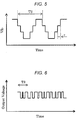
- FIG. 5 is a waveform diagram of the output signal in a case where the signal pulse having a period T2 shorter than T1 is input to the open drain circuit of FIG. 3 .
- the switching time interval is the same between the conduction and the non-conduction of each transistor since there is no change in the delay time ⁇ .
- the waveform period becomes shorter than that in FIG. 4 .
- FIG. 6 is a waveform diagram of the output signal in a case where the signal pulse having a period T3 ( ⁇ 4 ⁇ ) is input to the open drain circuit of FIG. 3 .
- the transistor Tr1 performs the next switching operation before the transistor Tr3 operates at 2 ⁇ after the transistor Tr1 is switched. Therefore, since the open drain transistors Tr1 to Tr3 all are not in the same operation state (conduction or non-conduction), the signal waveform is not possible to reach an upper limit (Hi level) and a lower limit (Low level). In other words, the peak value of the output signal becomes small, and the period becomes shorter than T3 and does not become constant.
- the invention relates to an open drain circuit in which a plurality of switching elements are connected to the output terminal in parallel to provide a time difference in operation timing of the respective switching elements so as to suppress a steep change in the waveform, and an object thereof is to avoid an abnormal waveform of the output signal as illustrated in FIG. 6 .
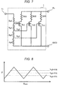
- FIG. 7 is a circuit diagram of an open drain circuit 1 according to a first embodiment of the invention.
- three open drain transistors Tr1 to Tr3 each are connected to the output terminal Fo through current limit resistors Rd1 to Rd3.
- an input signal Vi is input to drive the transistors Tr1 to Tr3.
- Vg1 to Vg3 obtained by dividing the input signal Vi using voltage-dividing resistors Rg1 to Rg4 are input to the gate terminals of the transistors Tr1 to Tr3, respectively.
- Vg 1 Vi ⁇ Rg 2 + Rg 3 + Rg 4 / Rg 1 + Rg 2 + Rg 3 + Rg 4
- Vg 2 Vi ⁇ Rg 3 + Rg 4 / Rg 1 + Rg 2 + Rg 3 + Rg 4
- Vg 3 Vi ⁇ Rg 4 / Rg 1 + Rg 2 + Rg 3 + Rg 4
- FIG. 8 is a waveform diagram of the input signal Vi.
- a triangular wave is used for example.
- the transistors Tr1 to Tr3 reach the threshold voltage Vth at different voltage values of the triangular wave. Therefore, the respective transistors are switched at timings different from each other.
- FIG. 9 is a diagram illustrating an exemplary configuration of a frequency measurement circuit 2 which is connected to the open drain circuit 1.
- the frequency measurement circuit 2 is provided with a frequency meter 3, a pull-up power source Vp, and the pull-up resistor Rp.
- An input terminal Input of the frequency meter 3 is connected to the output terminal Fo of the open drain circuit 1, and further connected to the pull-up power source Vp through the pull-up resistor Rp.
- FIG. 10 is a waveform diagram of the output voltage Vfo when the input signal Vi of the triangular wave is input to the open drain circuit 1 in the circuit configuration of FIG. 9 .
- the respective transistors are switched when the input signal Vi becomes the values represented by Equations 9 to 11. Therefore, the output voltage Vfo changes in a stepwise shape as illustrated in FIG. 10 .
- the output voltage Vfo when the transistors Tr1 to Tr3 are in a non-conductive state is set to Vfo0
- the output voltage Vfo when the transistor Tr1 is in the conductive state and the transistors Tr2 and Tr3 are in the non-conductive state is set to Vfo1
- the output voltage Vfo when the transistors Tr1 and Tr2 are in the conductive state and the transistor Tr3 is in the non-conductive state is set to Vfo2
- the output voltage Vfo when the transistors Tr1 to Tr3 are in the conductive state is set to Vfo3.
- Rd12 is a combined resistor obtained by connecting the resistors Rd1 and Rd2 in parallel, and expressed by the following Equation 16.
- Rd123 is a combined resistor obtained by connecting the resistors Rd1 to Rd3 in parallel, and expressed by the following Equation 17.
- Rd 12 Rd 1 ⁇ Rd 2 / Rd 1 + Rd 2
- Rd 123 Rd 1 ⁇ Rd 2 ⁇ Rd 3 / Rd 1 ⁇ Rd 2 + Rd 2 ⁇ Rd 3 + Rd 3 ⁇ Rd 1
- FIG. 11 illustrates a waveform of the output voltage Vfo in a case where a period of the input signal Vi changes in the circuit configuration of FIG. 9 .
- the time difference between the switching timings of the respective transistors when the period of Vi is T1 is ⁇ 1, and the time difference between the switching timings when the period of Vi is T2 is ⁇ 2.
- the switching timings of Tr1 to Tr3 depend on the potential of Vi. Therefore, when the period of Vi (the triangular wave) changes, the time difference between the switching timings of the respective transistors is in proportion to the period.
- T1, T2, ⁇ 1, and ⁇ 2 in FIG. 11 is expressed by the following Equation 18.
- T 1 / T 2 ⁇ 1 / ⁇ 2
- the open drain circuit 1 is provided with the delay circuit (the voltage-dividing circuit in the first embodiment) which deviates the switching timings for each of the respective transistors Tr1 to Tr3.
- the delay circuit causes the delay time interval ⁇ between the respective transistors to be changed according to the frequency of the input signal Vi with respect to the open drain circuit 1. Therefore, the delay time interval ⁇ is also shortened when the period of the input signal Vi is shortened, so that it is possible to suppress an abnormality in waveform of the output signal as illustrated in FIG. 6 .
- the information is represented by the frequency of the input signal Vi, and the frequency measurement circuit 2 measures the frequency. Therefore, in a case where the information is acquired, it is possible to suppress an abnormality in measurement as illustrated in FIG. 6 .
- the voltages Vfo1 to Vfo3 when the output voltage Vfo is switched in a stepwise shape are obtained by divided by the pull-up power source Vp using the pull-up resistor Rp and the current limit resistors Rd1 to Rd3.
- the pull-up resistor Rp and the current limit resistors Rd1 to Rd3 may be manufactured by a semiconductor process in many cases.
- a resistor manufactured by the semiconductor process may have a deviation in resistance (for example, about ⁇ 20%).
- the open drain circuit 1 and the frequency measurement circuit 2 are manufactured separately.
- the pull-up resistor Rp and the current limit resistors Rd1 to Rd3 have a large deviation in a ratio of resistance value and in a ratio of temperature property of the resistance. If there occurs such a deviation in resistance value, the following problems are caused in real products.
- the voltage Vc is set for comparison with the output voltage Vfo.
- the comparison voltage Vc is set to a voltage between 0 (V) and the pull-up voltage Vp.
- the frequency meter 3 measures a frequency and a period of an output signal Vfo by measuring a time when a magnitude relation between Vfo and Vc is changed.
- FIG. 12 is an exemplary waveform in which the output signal Vfo and the comparison voltage Vc do not intersect.
- the output voltage Vfo is always larger than the comparison voltage Vc. Therefore, the frequency meter 3 is not possible to measure the frequency of the output signal Vfo.
- Equations 13 to 15 when the resistance values of the current limit resistors Rd1 to Rd3 are increasingly deviated with respect to the resistance value of the pull-up resistor Rp, Vfo1 to Vfo3 are also increased, which causes a situation as illustrated in FIG. 12 .
- an exemplary circuit coping with such a problem will be described.
- FIG. 13 is a circuit diagram of the open drain circuit 1 according to the second embodiment.
- the open drain circuit 1 of FIG. 13 is configured such that the current limit resistor Rd3 is not provided in the circuit configuration illustrated in FIG. 7 and the drain terminal and the output terminal Fo of the transistor Tr3 are short-circuited.
- the output voltage Vfo becomes 0 (V) when Tr3 comes to a conductive state. Therefore, Vfo can become a potential lower than that of Vc regardless of the deviation in resistance of the pull-up resistor Rp and the current limit resistors Rd1 to Rd3.
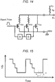
- FIG. 14 illustrates a circuit configuration from which the current limit resistor connected to the drain terminal of the transistor Tr3 is removed from the conventional open drain circuit illustrated in FIG. 3 , and thus the drain terminal is short-circuited with the output terminal Fo.
- a defect described below will be caused when the drain terminal of the transistor Tr3 is short-circuited with the output terminal Fo similarly to the second embodiment.
- an order of switching the transistors Tr1 to Tr3 from the non-conduction to the conduction is equal to the order from the conduction to the non-conduction. In other words, Tr1 is first switched and Tr3 is finally switched in either case.
- the output voltage Vfo is switched in a stepwise shape.
- Vfo remains at 0 (V) during a period when Tr3 is in conduction even Tr1 and Tr2 are in non-conduction. Thereafter, Vfo becomes the same potential as that of the pull-up voltage Vp when Tr3 is switched to the non-conduction. Tr3 comes to the conductive state to cause the output terminal Fo to be short-circuited to GND.
- FIG. 15 is a diagram illustrating a waveform of the output signal of the open drain circuit of FIG. 14 .
- the waveform is switched at one time without changing in a stepwise shape when the output waveform is switched from a low potential (low level) to a high potential (high level).
- the output waveform is steeply switched in this way, the effect of reducing radiation noises may be lessened.
- Tr3 having no current limit resistor is finally switched in a case where the open drain transistors Tr1 to Tr3 are switched from the non-conduction to the conduction, and Tr3 having no current limit resistor is firstly switched in the case of the order of switching from the conduction to the non-conduction is switched.
- the order of switching the open drain transistors Tr1 to Tr3 from the non-conduction to the conduction is in reverse to the order from the conduction to the non-conduction.
- Tr3 is finally switched in the case of switching from the non-conduction to the conduction, and Tr3 is firstly switched in the case of switching from the conduction to the non-conduction. Therefore, in the open drain circuit 1 according to the first and second embodiments, it is possible to suppress the steep change in output waveform illustrated in FIG. 15 .
- the open drain circuit 1 according to the second embodiment can suppress the problem as illustrated in FIG. 12 in that the resistance values of the pull-up resistor Rp and the current limit resistors Rd1 to Rd3 are deviated. Furthermore, it is possible to suppress a steep change in output waveform as illustrated in FIG. 15 in a case where the similar configuration is employed to the conventional open drain circuit.
- the drain terminal of Tr3 has been short-circuited with the output terminal Fo, and the other transistors may be short-circuited in the same way.
- the drain terminal of Tr2 may be short-circuited with the output terminal Fo.
- FIG. 16 is a diagram illustrating a waveform of the output signal of the open drain circuit 1 according to a third embodiment of the invention.
- a plurality of time differences ⁇ are provided in the switching timing between the respective open drain transistors.
- the time difference between Tr1 and Tr2 is ⁇ 1
- the time difference between Tr2 and Tr3 is ⁇ 2. Since ⁇ 1 and ⁇ 2 are determined according to Equations 9 to 11, ⁇ 1 and ⁇ 2 can be adjusted as illustrated in FIG. 16 by adjusting a voltage division ratio of the voltage-dividing resistors Rg1 to Rg4.
- a delay time interval ( ⁇ 1) of the switching element to be switched early is smaller than a delay time interval ( ⁇ 2) of the switching element to be switched later.
- the delay time interval ( ⁇ 2) of the switching element to be switched early is larger than the delay time interval ( ⁇ 1) of the switching element to be switched later. In other words, ⁇ 1 and ⁇ 2 both are constant.
- FIG. 17 is a diagram illustrating a modification of the open drain circuit 1 according to the third embodiment.
- the open drain circuit 1 illustrated in FIG. 17 is provided with a microcontroller 4 which realizes such a configuration.
- the microcontroller 4 receives the input signal Vi, calculates a desired timing of switching the respective transistors according to Vi, and outputs Vth to the gate terminals of the respective transistors at that timing.
- FIG. 18 is an exemplary waveform of the output signal in the circuit configuration of FIG. 17 .
- the delay time interval ( ⁇ 1) of the switching element to be switched early is smaller than the delay time interval ( ⁇ 2) of the switching element to be switched later.
- the delay time interval ( ⁇ 2) of the switching element to be switched early is smaller than the delay time interval ( ⁇ 1) of the switching element to be switched later. In other words, ⁇ 1 and ⁇ 2 change according to time.
- a capacitor, a resistor, and a diode may be provided as a surge protection element and a protection element against static discharge.
- a plurality of switching time differences as illustrated in FIGS. 16 and 18 .
- the output waveform according to the third embodiment is suitable to such as case.
- FIG. 19 is a diagram illustrating a configuration of a thermal-type flow meter 100 according to a fourth embodiment of the invention.
- the thermal-type flow meter 100 is a sensor to measure a flow rate of air, and provided with a measuring element 5, a signal generator 6, and the open drain circuit 1 according to the first to third embodiments.
- the measuring element 5 measures a flow rate of air, and outputs a meter voltage Vm corresponding to the measurement result.
- the signal generator 6 generates a periodic signal expressing the measurement result indicated by the meter voltage Vm using a frequency, and outputs the periodic signal to the open drain circuit 1 as the input signal Vi.
- the thermal-type flow meter 100 shows the flow rate of air using the frequency of the periodic signal. Therefore, it is desirable that the open drain circuit 1 according to the first to third embodiments be used.
- the invention is not limited to the above embodiments, and includes various modifications.
- the above embodiments are merely given to describe the invention in detail to help easy understanding, and there is no need to provide all the configurations described above. For example, the following modifications can be considered.
- the above embodiments have been described on an assumption that a field effect transistor (FET) is used as the open drain transistor, but the same configuration of the invention can be employed even in a case where a bipolar transistor is used.
- the same configuration of the invention can be employed in a circuit configuration in which the output signal is switched in a stepwise shape between the high level and the low level at every time when the respective switching elements connected at multiple stages are switched.
- the triangular wave has been used as the input signal Vi, and the same configuration of the invention can be employed even in a case where other periodic signal such as a sinusoidal wave or a trapezoid wave is used.
- Other correspondence relations may be employed as long as ⁇ is increased or decreased according to increase/decrease of Vi.
Landscapes
- Physics & Mathematics (AREA)
- Engineering & Computer Science (AREA)
- Computer Hardware Design (AREA)
- Fluid Mechanics (AREA)
- General Physics & Mathematics (AREA)
- Computing Systems (AREA)
- General Engineering & Computer Science (AREA)
- Mathematical Physics (AREA)
- Electronic Switches (AREA)
- Measuring Volume Flow (AREA)
Claims (7)
- Thermischer Durchflussmesser (100), der konfiguriert ist, ein Ausgangssignal (Vfo) auszugeben, und Folgendes umfasst:einen Signalgenerator (6), der ein periodisches Signal (Vi), das die Durchflussmenge angibt, unter Verwendung einer Frequenz erzeugt;eine Nebenschlussschaltung, die durch mehrere parallel geschaltete Schaltelemente (Tr1, Tr2, Tr3) konfiguriert ist und das Ausgangssignal (Vfo), das dem periodischen Signal (Vi) entspricht, ausgibt; undeine Verzögerungsschaltung (D), die eine Betriebsdauer jedes Schaltelements (Tr1, Tr2, Tr3) verzögert, derart, dass die jeweiligen Schaltelemente (Tr1, Tr2, Tr3) in unterschiedlichen Phasen des periodischen Signals (Vi) eingeschaltet werden,wobei die Nebenschlussschaltung konfiguriert ist, einen Signalpegel des Ausgangssignals (Vfo) von einem hohen Pegel stufenweise abzusenken, wann immer eines der Schaltelemente (Tr1, Tr2, Tr3) eingeschaltet wird, und den Signalpegel des Ausgangssignals (Vfo) unter einen tiefen Pegel fallen zu lassen, wenn sämtliche Schaltelemente (Tr1, Tr2, Tr3) eingeschaltet sind, undwobei die Verzögerungsschaltung (D) dafür ausgelegt ist, die verzögerte Zeitdauer (τ1, τ2, τ3) so zu ändern, dass sie kürzer wird, wenn die Frequenz des periodischen Signals (Vi) zunimmt, und dafür ausgelegt ist, die verzögerte Zeitdauer (τ1, τ2, τ3) so zu ändern, dass sie länger wird, wenn die Frequenz des periodischen Signals (Vi) abnimmt,wobei die Verzögerungsschaltung (D) durch eine Spannungsteilungsschaltung konfiguriert ist, die eine an einen Gate-Anschluss jedes Schaltelements (Tr1, Tr2, Tr3) angelegte Spannung so unterteilt, dass sie für jedes Schaltelement (Tr1, Tr2, Tr3) unterschiedliche Werte hat, oderwobei die Verzögerungsschaltung (D) durch eine Rechenschaltung (4) konfiguriert ist, die die verzögerte Zeitdauer (τ1, τ2, τ3) entsprechend einer Periode des periodischen Signals (Vi) berechnet und das Schaltelement (Tr1, Tr2, Tr3) in Übereinstimmung mit der Zeitdauer ansteuert,wobei die Verzögerungsschaltung (D) dafür ausgelegt ist, die verzögerte Zeitdauer (τ1, τ2, τ3) in der Weise einzustellen, dass die verzögerte Zeitdauer zwischen irgendwelchen Schaltelementen (Tr1, Tr2, Tr3) von der verzögerten Zeitdauer zwischen irgendwelchen anderen Schaltelementen (Tr1, Tr2, Tr3) verschieden ist.
- Thermischer Durchflussmesser (100) nach Anspruch 1,
wobei die Verzögerungsschaltung (D) dafür ausgelegt ist, die verzögerte Zeitdauer (τ1, τ2, τ3) proportional zur Frequenz des periodischen Signals (Vi) zu ändern. - Thermischer Durchflussmesser (100) nach Anspruch 1,
wobei wenigstens eines der Schaltelemente (Tr1, Tr2, Tr3) einen Strombegrenzungswiderstand (Rd1, Rd2, Rd3) enthält, der mit einem Ausgangsanschluss (Fo) des Ausgangssignals (Vfo) verbunden ist. - Thermischer Durchflussmesser (100) nach Anspruch 3,
wobei das Schaltelement (Tr3), das in einer letzten Stufe der Nebenschlussschaltung angeordnet ist, den Strombegrenzungswiderstand (Rd3) nicht enthält und die anderen Schaltelemente (Tr1, Tr2) der Nebenschlussschaltung den Strombegrenzungswiderstand (Rd1, Rd2) enthalten. - Thermischer Durchflussmesser (100) nach Anspruch 1,
wobei die Verzögerungsschaltung (D) dafür ausgelegt ist, eine Betriebszeit jedes Schaltelements (Tr1, Tr2, Tr3) in der Weise einzustellen, dass eine Reihenfolge des Schaltens der Schaltelemente (Tr1, Tr2, Tr3) der Nebenschlussschaltung von einem EIN-Zustand in einen AUS-Zustand in eine Reihenfolge des Schaltens von dem AUS-Zustand in den EIN-Zustand umgekehrt wird. - Thermischer Durchflussmesser (100) nach Anspruch 3,
wobei das Schaltelement (Tr3), das in einer letzten Stufe der Nebenschlussschaltung angeordnet ist, den Strombegrenzungswiderstand (Rd3) nicht enthält und die anderen Schaltelemente (Tr1, Tr2) der Nebenschlussschaltung den Strombegrenzungswiderstand (Rd1, Rd2) enthalten,
wobei die Verzögerungsschaltung (D) dafür ausgelegt ist, eine Betriebszeit jedes Schaltelements (Tr1, Tr2, Tr3) in der Weise einzustellen, dass eine Reihenfolge des Schaltens der Schaltelemente (Tr1, Tr2, Tr3) der Nebenschlussschaltung von einem EIN-Zustand in einen AUS-Zustand in eine Reihenfolge des Schaltens von dem AUS-Zustand in den EIN-Zustand umgekehrt wird und
wobei die Verzögerungsschaltung (D) dafür ausgelegt ist, schließlich das Schaltelement (Tr3), das keinen Strombegrenzungswiderstand (Rd3) enthält, einzuschalten, wenn das Ausgangssignal (Vfo) von dem hohen Pegel zu dem tiefen Pegel geschaltet wird, und das Schaltelement (Tr3), das keinen Strombegrenzungswiderstand (Rd3) besitzt, erstmals ausschaltet, wenn das Ausgangssignal (Vfo) von dem tiefen Pegel zu dem hohen Pegel geschaltet wird. - Thermischer Durchflussmesser (100) nach Anspruch 1,
wobei der Signalgenerator (6) dafür ausgelegt ist, ein Dreieckwellensignal als das periodische Signal (Vi) zu erzeugen.
Applications Claiming Priority (2)
| Application Number | Priority Date | Filing Date | Title |
|---|---|---|---|
| JP2014112979 | 2014-05-30 | ||
| PCT/JP2015/064844 WO2015182531A1 (ja) | 2014-05-30 | 2015-05-25 | 熱式流量計 |
Publications (3)
| Publication Number | Publication Date |
|---|---|
| EP3150977A1 EP3150977A1 (de) | 2017-04-05 |
| EP3150977A4 EP3150977A4 (de) | 2018-02-14 |
| EP3150977B1 true EP3150977B1 (de) | 2020-12-16 |
Family
ID=54698862
Family Applications (1)
| Application Number | Title | Priority Date | Filing Date |
|---|---|---|---|
| EP15798963.3A Not-in-force EP3150977B1 (de) | 2014-05-30 | 2015-05-25 | Thermischer durchflussmesser |
Country Status (5)
| Country | Link |
|---|---|
| US (1) | US9958306B2 (de) |
| EP (1) | EP3150977B1 (de) |
| JP (1) | JP6185168B2 (de) |
| CN (1) | CN106461441B (de) |
| WO (1) | WO2015182531A1 (de) |
Families Citing this family (2)
| Publication number | Priority date | Publication date | Assignee | Title |
|---|---|---|---|---|
| DE112019002432B4 (de) * | 2018-06-13 | 2025-08-07 | Hitachi Astemo, Ltd. | Detektionsvorrichtung für physikalische grössen |
| CN109470325B (zh) * | 2018-09-20 | 2021-03-16 | 北京七星华创流量计有限公司 | 气体流量测量方法、装置以及控制系统和气体质量流量计 |
Family Cites Families (16)
| Publication number | Priority date | Publication date | Assignee | Title |
|---|---|---|---|---|
| US4043196A (en) * | 1976-02-09 | 1977-08-23 | Technology Incorporated | Method and apparatus for effecting fluid flow measurement in a single sensor |
| JPS6435218A (en) | 1987-07-30 | 1989-02-06 | Hitachi Ltd | Hot wire type air flowmeter |
| JPH01228214A (ja) | 1988-03-08 | 1989-09-12 | Matsushita Electron Corp | 半導体集積回路 |
| JP3463757B2 (ja) | 1993-04-08 | 2003-11-05 | 株式会社日立製作所 | エンジン制御装置及びこれに用いる空気流量計 |
| JPH0897701A (ja) * | 1994-09-21 | 1996-04-12 | Mitsubishi Electric Corp | 半導体回路 |
| JPH08228141A (ja) | 1995-02-21 | 1996-09-03 | Kawasaki Steel Corp | 出力バッファ回路 |
| JPH11239046A (ja) | 1998-02-23 | 1999-08-31 | Nec Corp | トランジスタ駆動装置及びその駆動方法 |
| JP2001285051A (ja) | 2000-03-29 | 2001-10-12 | Kawasaki Steel Corp | 出力バッファ回路 |
| JP3808038B2 (ja) * | 2003-01-14 | 2006-08-09 | 株式会社日立製作所 | 周波数出力型熱線式流量計 |
| JP4167201B2 (ja) | 2004-04-21 | 2008-10-15 | 株式会社日立製作所 | 周波数出力回路 |
| JP3953492B2 (ja) | 2004-04-22 | 2007-08-08 | Necエレクトロニクス株式会社 | 出力バッファ回路 |
| US8115540B2 (en) * | 2006-09-14 | 2012-02-14 | Nec Corporation | Amplifying apparatus, method of output control and control program |
| JP5112184B2 (ja) * | 2008-06-24 | 2013-01-09 | 日立オートモティブシステムズ株式会社 | 流量計及び流量計測装置 |
| JP5999592B2 (ja) * | 2011-09-07 | 2016-09-28 | ローム株式会社 | 受信回路、半導体装置、センサ装置 |
| US9631965B2 (en) * | 2012-02-15 | 2017-04-25 | Sensortechnics GmbH | Offset compensation for flow sensing devices |
| CN103837243B (zh) * | 2014-03-27 | 2016-08-24 | 卓捷创芯科技(深圳)有限公司 | 时间域集成温度传感器 |
-
2015
- 2015-05-25 CN CN201580028619.6A patent/CN106461441B/zh not_active Expired - Fee Related
- 2015-05-25 EP EP15798963.3A patent/EP3150977B1/de not_active Not-in-force
- 2015-05-25 WO PCT/JP2015/064844 patent/WO2015182531A1/ja not_active Ceased
- 2015-05-25 US US15/311,206 patent/US9958306B2/en active Active
- 2015-05-25 JP JP2016523478A patent/JP6185168B2/ja not_active Expired - Fee Related
Non-Patent Citations (1)
| Title |
|---|
| None * |
Also Published As
| Publication number | Publication date |
|---|---|
| WO2015182531A1 (ja) | 2015-12-03 |
| CN106461441B (zh) | 2019-09-06 |
| JPWO2015182531A1 (ja) | 2017-04-20 |
| JP6185168B2 (ja) | 2017-08-23 |
| CN106461441A (zh) | 2017-02-22 |
| US20170082472A1 (en) | 2017-03-23 |
| EP3150977A4 (de) | 2018-02-14 |
| US9958306B2 (en) | 2018-05-01 |
| EP3150977A1 (de) | 2017-04-05 |
Similar Documents
| Publication | Publication Date | Title |
|---|---|---|
| CN109473950B (zh) | 用于保护功率开关的电路和方法 | |
| JP7004585B2 (ja) | 半導体装置、負荷駆動システムおよびインダクタ電流の電流検出方法 | |
| US10700678B2 (en) | Drive control circuit for power semiconductor element | |
| CN101174827B (zh) | 复位装置 | |
| JP6498473B2 (ja) | スイッチ駆動回路 | |
| US20150364913A1 (en) | Load driving circuit | |
| JP6436230B2 (ja) | 駆動回路 | |
| US20140203846A1 (en) | Method for Driving a Load | |
| US20050104650A1 (en) | Method for switching driving of a semiconductor switching element | |
| EP3150977B1 (de) | Thermischer durchflussmesser | |
| US10958065B2 (en) | Switching circuit | |
| EP3563641B1 (de) | Adaptive ausschaltverzögerungszeitkompensation für led-steuergerät | |
| KR101171561B1 (ko) | 펄스 폭에 따라 동작하는 슈미트 트리거 회로 | |
| JP5180714B2 (ja) | 負荷短絡保護回路 | |
| US9077294B2 (en) | Measurement of the output current of an amplifier circuit | |
| US20120119763A1 (en) | Circuits and Methods for Sensing Resistance | |
| US11489434B2 (en) | Power transducer including a rate of voltage change detection circuit | |
| JP7709394B2 (ja) | 半導体素子のリーク電流検出回路 | |
| US9883611B2 (en) | Fan control circuit | |
| US10656032B2 (en) | Temperature sensor in an integrated circuit and method of calibrating the temperature sensor | |
| CN103592519A (zh) | 可检测突波信号特性的突波检测装置 | |
| Summatta et al. | Three-stage window comparator circuit with MOSFET-resistor voltage reference | |
| CN102955115A (zh) | 功率测试系统 | |
| US11029365B2 (en) | Semiconductor device | |
| JP7155082B2 (ja) | 電子回路 |
Legal Events
| Date | Code | Title | Description |
|---|---|---|---|
| STAA | Information on the status of an ep patent application or granted ep patent |
Free format text: STATUS: THE INTERNATIONAL PUBLICATION HAS BEEN MADE |
|
| PUAI | Public reference made under article 153(3) epc to a published international application that has entered the european phase |
Free format text: ORIGINAL CODE: 0009012 |
|
| STAA | Information on the status of an ep patent application or granted ep patent |
Free format text: STATUS: REQUEST FOR EXAMINATION WAS MADE |
|
| 17P | Request for examination filed |
Effective date: 20170102 |
|
| AK | Designated contracting states |
Kind code of ref document: A1 Designated state(s): AL AT BE BG CH CY CZ DE DK EE ES FI FR GB GR HR HU IE IS IT LI LT LU LV MC MK MT NL NO PL PT RO RS SE SI SK SM TR |
|
| AX | Request for extension of the european patent |
Extension state: BA ME |
|
| DAV | Request for validation of the european patent (deleted) | ||
| DAX | Request for extension of the european patent (deleted) | ||
| A4 | Supplementary search report drawn up and despatched |
Effective date: 20180112 |
|
| RIC1 | Information provided on ipc code assigned before grant |
Ipc: H03K 17/284 20060101ALI20180108BHEP Ipc: G01F 1/698 20060101AFI20180108BHEP Ipc: H03K 17/16 20060101ALI20180108BHEP Ipc: H03K 19/0175 20060101ALI20180108BHEP |
|
| STAA | Information on the status of an ep patent application or granted ep patent |
Free format text: STATUS: EXAMINATION IS IN PROGRESS |
|
| 17Q | First examination report despatched |
Effective date: 20190311 |
|
| GRAP | Despatch of communication of intention to grant a patent |
Free format text: ORIGINAL CODE: EPIDOSNIGR1 |
|
| STAA | Information on the status of an ep patent application or granted ep patent |
Free format text: STATUS: GRANT OF PATENT IS INTENDED |
|
| INTG | Intention to grant announced |
Effective date: 20200924 |
|
| GRAS | Grant fee paid |
Free format text: ORIGINAL CODE: EPIDOSNIGR3 |
|
| GRAA | (expected) grant |
Free format text: ORIGINAL CODE: 0009210 |
|
| STAA | Information on the status of an ep patent application or granted ep patent |
Free format text: STATUS: THE PATENT HAS BEEN GRANTED |
|
| AK | Designated contracting states |
Kind code of ref document: B1 Designated state(s): AL AT BE BG CH CY CZ DE DK EE ES FI FR GB GR HR HU IE IS IT LI LT LU LV MC MK MT NL NO PL PT RO RS SE SI SK SM TR |
|
| REG | Reference to a national code |
Ref country code: GB Ref legal event code: FG4D |
|
| RIN1 | Information on inventor provided before grant (corrected) |
Inventor name: TERADA DAISUKE Inventor name: HOSOKAWA TAKEO Inventor name: ANDO RYO |
|
| REG | Reference to a national code |
Ref country code: DE Ref legal event code: R096 Ref document number: 602015063610 Country of ref document: DE |
|
| REG | Reference to a national code |
Ref country code: IE Ref legal event code: FG4D |
|
| RIN2 | Information on inventor provided after grant (corrected) |
Inventor name: ANDO RYO Inventor name: HOSOKAWA TAKEO Inventor name: TERADA DAISUKE |
|
| REG | Reference to a national code |
Ref country code: AT Ref legal event code: REF Ref document number: 1346017 Country of ref document: AT Kind code of ref document: T Effective date: 20210115 |
|
| PG25 | Lapsed in a contracting state [announced via postgrant information from national office to epo] |
Ref country code: NO Free format text: LAPSE BECAUSE OF FAILURE TO SUBMIT A TRANSLATION OF THE DESCRIPTION OR TO PAY THE FEE WITHIN THE PRESCRIBED TIME-LIMIT Effective date: 20210316 Ref country code: FI Free format text: LAPSE BECAUSE OF FAILURE TO SUBMIT A TRANSLATION OF THE DESCRIPTION OR TO PAY THE FEE WITHIN THE PRESCRIBED TIME-LIMIT Effective date: 20201216 Ref country code: RS Free format text: LAPSE BECAUSE OF FAILURE TO SUBMIT A TRANSLATION OF THE DESCRIPTION OR TO PAY THE FEE WITHIN THE PRESCRIBED TIME-LIMIT Effective date: 20201216 Ref country code: GR Free format text: LAPSE BECAUSE OF FAILURE TO SUBMIT A TRANSLATION OF THE DESCRIPTION OR TO PAY THE FEE WITHIN THE PRESCRIBED TIME-LIMIT Effective date: 20210317 |
|
| REG | Reference to a national code |
Ref country code: AT Ref legal event code: MK05 Ref document number: 1346017 Country of ref document: AT Kind code of ref document: T Effective date: 20201216 |
|
| REG | Reference to a national code |
Ref country code: NL Ref legal event code: MP Effective date: 20201216 |
|
| PG25 | Lapsed in a contracting state [announced via postgrant information from national office to epo] |
Ref country code: SE Free format text: LAPSE BECAUSE OF FAILURE TO SUBMIT A TRANSLATION OF THE DESCRIPTION OR TO PAY THE FEE WITHIN THE PRESCRIBED TIME-LIMIT Effective date: 20201216 Ref country code: LV Free format text: LAPSE BECAUSE OF FAILURE TO SUBMIT A TRANSLATION OF THE DESCRIPTION OR TO PAY THE FEE WITHIN THE PRESCRIBED TIME-LIMIT Effective date: 20201216 Ref country code: BG Free format text: LAPSE BECAUSE OF FAILURE TO SUBMIT A TRANSLATION OF THE DESCRIPTION OR TO PAY THE FEE WITHIN THE PRESCRIBED TIME-LIMIT Effective date: 20210316 |
|
| PG25 | Lapsed in a contracting state [announced via postgrant information from national office to epo] |
Ref country code: NL Free format text: LAPSE BECAUSE OF FAILURE TO SUBMIT A TRANSLATION OF THE DESCRIPTION OR TO PAY THE FEE WITHIN THE PRESCRIBED TIME-LIMIT Effective date: 20201216 Ref country code: HR Free format text: LAPSE BECAUSE OF FAILURE TO SUBMIT A TRANSLATION OF THE DESCRIPTION OR TO PAY THE FEE WITHIN THE PRESCRIBED TIME-LIMIT Effective date: 20201216 |
|
| REG | Reference to a national code |
Ref country code: LT Ref legal event code: MG9D |
|
| PG25 | Lapsed in a contracting state [announced via postgrant information from national office to epo] |
Ref country code: EE Free format text: LAPSE BECAUSE OF FAILURE TO SUBMIT A TRANSLATION OF THE DESCRIPTION OR TO PAY THE FEE WITHIN THE PRESCRIBED TIME-LIMIT Effective date: 20201216 Ref country code: CZ Free format text: LAPSE BECAUSE OF FAILURE TO SUBMIT A TRANSLATION OF THE DESCRIPTION OR TO PAY THE FEE WITHIN THE PRESCRIBED TIME-LIMIT Effective date: 20201216 Ref country code: SM Free format text: LAPSE BECAUSE OF FAILURE TO SUBMIT A TRANSLATION OF THE DESCRIPTION OR TO PAY THE FEE WITHIN THE PRESCRIBED TIME-LIMIT Effective date: 20201216 Ref country code: LT Free format text: LAPSE BECAUSE OF FAILURE TO SUBMIT A TRANSLATION OF THE DESCRIPTION OR TO PAY THE FEE WITHIN THE PRESCRIBED TIME-LIMIT Effective date: 20201216 Ref country code: PT Free format text: LAPSE BECAUSE OF FAILURE TO SUBMIT A TRANSLATION OF THE DESCRIPTION OR TO PAY THE FEE WITHIN THE PRESCRIBED TIME-LIMIT Effective date: 20210416 Ref country code: RO Free format text: LAPSE BECAUSE OF FAILURE TO SUBMIT A TRANSLATION OF THE DESCRIPTION OR TO PAY THE FEE WITHIN THE PRESCRIBED TIME-LIMIT Effective date: 20201216 Ref country code: SK Free format text: LAPSE BECAUSE OF FAILURE TO SUBMIT A TRANSLATION OF THE DESCRIPTION OR TO PAY THE FEE WITHIN THE PRESCRIBED TIME-LIMIT Effective date: 20201216 |
|
| PG25 | Lapsed in a contracting state [announced via postgrant information from national office to epo] |
Ref country code: AT Free format text: LAPSE BECAUSE OF FAILURE TO SUBMIT A TRANSLATION OF THE DESCRIPTION OR TO PAY THE FEE WITHIN THE PRESCRIBED TIME-LIMIT Effective date: 20201216 Ref country code: PL Free format text: LAPSE BECAUSE OF FAILURE TO SUBMIT A TRANSLATION OF THE DESCRIPTION OR TO PAY THE FEE WITHIN THE PRESCRIBED TIME-LIMIT Effective date: 20201216 |
|
| REG | Reference to a national code |
Ref country code: DE Ref legal event code: R097 Ref document number: 602015063610 Country of ref document: DE |
|
| REG | Reference to a national code |
Ref country code: DE Ref legal event code: R081 Ref document number: 602015063610 Country of ref document: DE Owner name: HITACHI ASTEMO, LTD., HITACHINAKA-SHI, JP Free format text: FORMER OWNER: HITACHI AUTOMOTIVE SYSTEMS, LTD., HITACHINAKA-SHI, IBARAKI, JP |
|
| PG25 | Lapsed in a contracting state [announced via postgrant information from national office to epo] |
Ref country code: IS Free format text: LAPSE BECAUSE OF FAILURE TO SUBMIT A TRANSLATION OF THE DESCRIPTION OR TO PAY THE FEE WITHIN THE PRESCRIBED TIME-LIMIT Effective date: 20210416 |
|
| PLBE | No opposition filed within time limit |
Free format text: ORIGINAL CODE: 0009261 |
|
| STAA | Information on the status of an ep patent application or granted ep patent |
Free format text: STATUS: NO OPPOSITION FILED WITHIN TIME LIMIT |
|
| PG25 | Lapsed in a contracting state [announced via postgrant information from national office to epo] |
Ref country code: IT Free format text: LAPSE BECAUSE OF FAILURE TO SUBMIT A TRANSLATION OF THE DESCRIPTION OR TO PAY THE FEE WITHIN THE PRESCRIBED TIME-LIMIT Effective date: 20201216 Ref country code: AL Free format text: LAPSE BECAUSE OF FAILURE TO SUBMIT A TRANSLATION OF THE DESCRIPTION OR TO PAY THE FEE WITHIN THE PRESCRIBED TIME-LIMIT Effective date: 20201216 |
|
| 26N | No opposition filed |
Effective date: 20210917 |
|
| PG25 | Lapsed in a contracting state [announced via postgrant information from national office to epo] |
Ref country code: ES Free format text: LAPSE BECAUSE OF FAILURE TO SUBMIT A TRANSLATION OF THE DESCRIPTION OR TO PAY THE FEE WITHIN THE PRESCRIBED TIME-LIMIT Effective date: 20201216 Ref country code: DK Free format text: LAPSE BECAUSE OF FAILURE TO SUBMIT A TRANSLATION OF THE DESCRIPTION OR TO PAY THE FEE WITHIN THE PRESCRIBED TIME-LIMIT Effective date: 20201216 |
|
| REG | Reference to a national code |
Ref country code: CH Ref legal event code: PL |
|
| GBPC | Gb: european patent ceased through non-payment of renewal fee |
Effective date: 20210525 |
|
| PG25 | Lapsed in a contracting state [announced via postgrant information from national office to epo] |
Ref country code: MC Free format text: LAPSE BECAUSE OF FAILURE TO SUBMIT A TRANSLATION OF THE DESCRIPTION OR TO PAY THE FEE WITHIN THE PRESCRIBED TIME-LIMIT Effective date: 20201216 Ref country code: LI Free format text: LAPSE BECAUSE OF NON-PAYMENT OF DUE FEES Effective date: 20210531 Ref country code: LU Free format text: LAPSE BECAUSE OF NON-PAYMENT OF DUE FEES Effective date: 20210525 Ref country code: CH Free format text: LAPSE BECAUSE OF NON-PAYMENT OF DUE FEES Effective date: 20210531 |
|
| REG | Reference to a national code |
Ref country code: BE Ref legal event code: MM Effective date: 20210531 |
|
| PG25 | Lapsed in a contracting state [announced via postgrant information from national office to epo] |
Ref country code: SI Free format text: LAPSE BECAUSE OF FAILURE TO SUBMIT A TRANSLATION OF THE DESCRIPTION OR TO PAY THE FEE WITHIN THE PRESCRIBED TIME-LIMIT Effective date: 20201216 |
|
| PG25 | Lapsed in a contracting state [announced via postgrant information from national office to epo] |
Ref country code: IE Free format text: LAPSE BECAUSE OF NON-PAYMENT OF DUE FEES Effective date: 20210525 Ref country code: GB Free format text: LAPSE BECAUSE OF NON-PAYMENT OF DUE FEES Effective date: 20210525 |
|
| PG25 | Lapsed in a contracting state [announced via postgrant information from national office to epo] |
Ref country code: IS Free format text: LAPSE BECAUSE OF FAILURE TO SUBMIT A TRANSLATION OF THE DESCRIPTION OR TO PAY THE FEE WITHIN THE PRESCRIBED TIME-LIMIT Effective date: 20210416 Ref country code: FR Free format text: LAPSE BECAUSE OF NON-PAYMENT OF DUE FEES Effective date: 20210531 |
|
| PG25 | Lapsed in a contracting state [announced via postgrant information from national office to epo] |
Ref country code: BE Free format text: LAPSE BECAUSE OF NON-PAYMENT OF DUE FEES Effective date: 20210531 |
|
| PGFP | Annual fee paid to national office [announced via postgrant information from national office to epo] |
Ref country code: DE Payment date: 20220329 Year of fee payment: 8 |
|
| PG25 | Lapsed in a contracting state [announced via postgrant information from national office to epo] |
Ref country code: HU Free format text: LAPSE BECAUSE OF FAILURE TO SUBMIT A TRANSLATION OF THE DESCRIPTION OR TO PAY THE FEE WITHIN THE PRESCRIBED TIME-LIMIT; INVALID AB INITIO Effective date: 20150525 |
|
| PG25 | Lapsed in a contracting state [announced via postgrant information from national office to epo] |
Ref country code: CY Free format text: LAPSE BECAUSE OF FAILURE TO SUBMIT A TRANSLATION OF THE DESCRIPTION OR TO PAY THE FEE WITHIN THE PRESCRIBED TIME-LIMIT Effective date: 20201216 |
|
| REG | Reference to a national code |
Ref country code: DE Ref legal event code: R119 Ref document number: 602015063610 Country of ref document: DE |
|
| PG25 | Lapsed in a contracting state [announced via postgrant information from national office to epo] |
Ref country code: MK Free format text: LAPSE BECAUSE OF FAILURE TO SUBMIT A TRANSLATION OF THE DESCRIPTION OR TO PAY THE FEE WITHIN THE PRESCRIBED TIME-LIMIT Effective date: 20201216 Ref country code: DE Free format text: LAPSE BECAUSE OF NON-PAYMENT OF DUE FEES Effective date: 20231201 |
|
| PG25 | Lapsed in a contracting state [announced via postgrant information from national office to epo] |
Ref country code: TR Free format text: LAPSE BECAUSE OF FAILURE TO SUBMIT A TRANSLATION OF THE DESCRIPTION OR TO PAY THE FEE WITHIN THE PRESCRIBED TIME-LIMIT Effective date: 20201216 |
|
| PG25 | Lapsed in a contracting state [announced via postgrant information from national office to epo] |
Ref country code: MT Free format text: LAPSE BECAUSE OF FAILURE TO SUBMIT A TRANSLATION OF THE DESCRIPTION OR TO PAY THE FEE WITHIN THE PRESCRIBED TIME-LIMIT Effective date: 20201216 |