EP3167992A1 - Bleilötverbindungsstruktur und verfahren zu ihrer herstellung - Google Patents
Bleilötverbindungsstruktur und verfahren zu ihrer herstellung Download PDFInfo
- Publication number
- EP3167992A1 EP3167992A1 EP16187779.0A EP16187779A EP3167992A1 EP 3167992 A1 EP3167992 A1 EP 3167992A1 EP 16187779 A EP16187779 A EP 16187779A EP 3167992 A1 EP3167992 A1 EP 3167992A1
- Authority
- EP
- European Patent Office
- Prior art keywords
- solder
- solder layer
- lead
- layer
- joint
- Prior art date
- Legal status (The legal status is an assumption and is not a legal conclusion. Google has not performed a legal analysis and makes no representation as to the accuracy of the status listed.)
- Granted
Links
Images


Classifications
-
- H—ELECTRICITY
- H05—ELECTRIC TECHNIQUES NOT OTHERWISE PROVIDED FOR
- H05K—PRINTED CIRCUITS; CASINGS OR CONSTRUCTIONAL DETAILS OF ELECTRIC APPARATUS; MANUFACTURE OF ASSEMBLAGES OF ELECTRICAL COMPONENTS
- H05K3/00—Apparatus or processes for manufacturing printed circuits
- H05K3/30—Assembling printed circuits with electric components, e.g. with resistors
- H05K3/32—Assembling printed circuits with electric components, e.g. with resistors electrically connecting electric components or wires to printed circuits
- H05K3/34—Assembling printed circuits with electric components, e.g. with resistors electrically connecting electric components or wires to printed circuits by soldering
- H05K3/3465—Application of solder
-
- B—PERFORMING OPERATIONS; TRANSPORTING
- B23—MACHINE TOOLS; METAL-WORKING NOT OTHERWISE PROVIDED FOR
- B23K—SOLDERING OR UNSOLDERING; WELDING; CLADDING OR PLATING BY SOLDERING OR WELDING; CUTTING BY APPLYING HEAT LOCALLY, e.g. FLAME CUTTING; WORKING BY LASER BEAM
- B23K1/00—Soldering, e.g. brazing, or unsoldering
- B23K1/0008—Soldering, e.g. brazing, or unsoldering specially adapted for particular articles or work
- B23K1/0016—Soldering of electronic components
-
- B—PERFORMING OPERATIONS; TRANSPORTING
- B23—MACHINE TOOLS; METAL-WORKING NOT OTHERWISE PROVIDED FOR
- B23K—SOLDERING OR UNSOLDERING; WELDING; CLADDING OR PLATING BY SOLDERING OR WELDING; CUTTING BY APPLYING HEAT LOCALLY, e.g. FLAME CUTTING; WORKING BY LASER BEAM
- B23K20/00—Non-electric welding by applying impact or other pressure, with or without the application of heat, e.g. cladding or plating
- B23K20/02—Non-electric welding by applying impact or other pressure, with or without the application of heat, e.g. cladding or plating by means of a press ; Diffusion bonding
- B23K20/023—Thermo-compression bonding
- B23K20/026—Thermo-compression bonding with diffusion of soldering material
-
- B—PERFORMING OPERATIONS; TRANSPORTING
- B23—MACHINE TOOLS; METAL-WORKING NOT OTHERWISE PROVIDED FOR
- B23K—SOLDERING OR UNSOLDERING; WELDING; CLADDING OR PLATING BY SOLDERING OR WELDING; CUTTING BY APPLYING HEAT LOCALLY, e.g. FLAME CUTTING; WORKING BY LASER BEAM
- B23K35/00—Rods, electrodes, materials, or media, for use in soldering, welding, or cutting
- B23K35/22—Rods, electrodes, materials, or media, for use in soldering, welding, or cutting characterised by the composition or nature of the material
- B23K35/24—Selection of soldering or welding materials proper
- B23K35/26—Selection of soldering or welding materials proper with the principal constituent melting at less than 400°C
-
- B—PERFORMING OPERATIONS; TRANSPORTING
- B23—MACHINE TOOLS; METAL-WORKING NOT OTHERWISE PROVIDED FOR
- B23K—SOLDERING OR UNSOLDERING; WELDING; CLADDING OR PLATING BY SOLDERING OR WELDING; CUTTING BY APPLYING HEAT LOCALLY, e.g. FLAME CUTTING; WORKING BY LASER BEAM
- B23K35/00—Rods, electrodes, materials, or media, for use in soldering, welding, or cutting
- B23K35/22—Rods, electrodes, materials, or media, for use in soldering, welding, or cutting characterised by the composition or nature of the material
- B23K35/24—Selection of soldering or welding materials proper
- B23K35/26—Selection of soldering or welding materials proper with the principal constituent melting at less than 400°C
- B23K35/268—Pb as the principal constituent
-
- B—PERFORMING OPERATIONS; TRANSPORTING
- B23—MACHINE TOOLS; METAL-WORKING NOT OTHERWISE PROVIDED FOR
- B23K—SOLDERING OR UNSOLDERING; WELDING; CLADDING OR PLATING BY SOLDERING OR WELDING; CUTTING BY APPLYING HEAT LOCALLY, e.g. FLAME CUTTING; WORKING BY LASER BEAM
- B23K2101/00—Articles made by soldering, welding or cutting
- B23K2101/36—Electric or electronic devices
- B23K2101/38—Conductors
-
- H—ELECTRICITY
- H05—ELECTRIC TECHNIQUES NOT OTHERWISE PROVIDED FOR
- H05K—PRINTED CIRCUITS; CASINGS OR CONSTRUCTIONAL DETAILS OF ELECTRIC APPARATUS; MANUFACTURE OF ASSEMBLAGES OF ELECTRICAL COMPONENTS
- H05K2201/00—Indexing scheme relating to printed circuits covered by H05K1/00
- H05K2201/03—Conductive materials
- H05K2201/0332—Structure of the conductor
- H05K2201/0335—Layered conductors or foils
- H05K2201/0338—Layered conductor, e.g. layered metal substrate, layered finish layer or layered thin film adhesion layer
-
- H—ELECTRICITY
- H05—ELECTRIC TECHNIQUES NOT OTHERWISE PROVIDED FOR
- H05K—PRINTED CIRCUITS; CASINGS OR CONSTRUCTIONAL DETAILS OF ELECTRIC APPARATUS; MANUFACTURE OF ASSEMBLAGES OF ELECTRICAL COMPONENTS
- H05K3/00—Apparatus or processes for manufacturing printed circuits
- H05K3/30—Assembling printed circuits with electric components, e.g. with resistors
- H05K3/32—Assembling printed circuits with electric components, e.g. with resistors electrically connecting electric components or wires to printed circuits
- H05K3/34—Assembling printed circuits with electric components, e.g. with resistors electrically connecting electric components or wires to printed circuits by soldering
- H05K3/3465—Application of solder
- H05K3/3478—Application of solder preforms; Transferring prefabricated solder patterns
Definitions
- the present invention relates to a lead solder joint structure and a manufacturing method thereof that suppress the occurrence of phase transition of solder at the time of usage.
- solder is used in various apparatuses, recently, use of lead solder is restricted in some cases. On the other hand, the use of lead solder is not restricted in a field of aerospace. Since joint strength of a solder joint portion that uses such lead solder affects reliability of apparatuses, it is desired that the joint strength is high.
- Japanese Patent Application Laid-Open Publication No. 1993-259632 discloses a printed wiring board shown in Fig. 4 .
- an object of the art is to improve reliability of joint in a joint process.
- a conductor 102 which forms a wiring pattern made of a copper foil and which is used for soldering electric components to be mounted, is arranged on both surfaces (surface A and surface B) of a substrate 100.
- a solder layer (first solder layer) 105 which includes lead and an intermetallic compound of tin, is arranged on the conductor 102 of the surface A (one surface).
- a solder layer (second solder layer) 104 which is tin-lead based solder layer (tin-lead 63/37), is arranged on the conductor 102 of the surface B (the other surface).
- a melting point (227 degrees centigrade) of the solder layer 105 on the surface A is higher than a melting point (183 degrees centigrade) of the solder layer 104 on the surface B.
- the solder layers are formed on the conductors formed on both surfaces of the substrate 102, and the solder layer formed on the one surface is changed to an alloy of lead and an intermetallic compound of tin by carrying out the heating process. Since the melting point of the solder layer formed on the one surface is higher than the melting point of the solder layer formed on the other surface by virtue of the above mention, it is possible to prevent that a joint portion of an electric component, which has been mounted on the surface A set downward, is melted when melting the solder layer 104 on the surface B.
- the structure according to Japanese Patent Application Laid-Open Publication No. 1993-259632 increases the joint strength by making the melting temperature of the tin-based intermetallic compound, which is typically formed when phase transition of the lead solder takes place, different from the melting temperature of the alloy.
- the intermetallic compound is generally brittle as mentioned above, it is important to have the sufficient joint strength at the time of joint, and furthermore it is also necessary to avoid that the joint strength is degraded at the time of using an electronic device including the solder joint.
- the joint portion receives an impact of the heat cycle or the like, and consequently it is progressed that the joint portion deteriorates into the intermetallic compound and the metallic crystalline grains of the solder become coarse.
- a main object of the present invention is to provide lead solder joint structure and a manufacturing method thereof which can restrain degradation of the joint strength even if the high temperature or the heat cycle is applied.
- lead solder joint structure in which a first member is joined to a second member using lead solder, the structure comprising:
- a method for manufacturing lead solder joint structure in which a first member is joined to a second member using lead solder, the method comprising:
- the lead solder joint structure and the manufacturing method thereof which can restrain degradation of the joint strength even if the high temperature or the heat cycle is applied.
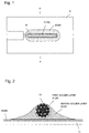
- Fig. 1 is a top view of a joint portion for explaining a lead solder joint structure according to the present exemplary embodiment
- Fig. 2 is a cross section view taken along A - A of Fig. 1 .
- Sn10 Sn: 10%, Ag: 2%, Pb: 88% ; solidus line: 267.8 degrees centigrade, liquidus line: 298.9 degrees centigrade
- lead solder Sn10
- FIG. 1 exemplifies lead solder joint structure 20 in which a wire (first member) 10 is joined to a conductor (second member) 11 by use of the Sn10 solder.
- a bus bar which is manufactured by use of a sheet of silver or a sheet of kovar plated with silver, is exemplified.
- the wire 10 a wiring member which is copper wire plated with silver is exemplified.
- the lead solder joint structure 20 includes a first solder layer 21 that is formed so as to include the wire 10 as a core, a second solder layer 22 which covers the first solder layer 21 and adheres to the conductor 11 through a third solder layer 24, and the third solder layer that exists between the second solder layer 22 and a solder joint surface side of the second member 11.
- the first solder layer 21 is a solder layer whose main constituent is a tin-copper based intermetallic compound.
- the second solder layer 22 is a solder layer whose main constituent is a lead-based alloy (that is, a solder layer which has a quite small amount of tin, and tin-based intermetallic compound).
- the third solder layer 24 is a solder layer whose main constituent is a tin-silver based intermetallic compound.
- the intermetallic compound is hard and brittle. Accordingly, the tin-copper based intermetallic compound and the tin-silver based intermetallic compound also have the same characteristics. Therefore, when the wire 10 or the conductor 11 is under stress caused by difference in expansion rate associating with heat cycles and the like, brittle fracture and the like may occur at the joint portion. Accordingly, there is a fear that reliability of joint is degraded.
- the intermetallic compound is gradually formed and the crystalline grains of the solder become coarse when an exposure time to a high temperature state becomes increasing not only continuously but also discontinuously during the course of usage even if a small amount of the intermetallic compound exists at the time of joint.
- the intermetallic compound is gradually formed at the joint portion soldered using the lead solder, and it is progressed that the crystalline grains of the solder become coarse in the forming process. As a result, the reliability of joint is degraded.
- the intermetallic compound is formed as much as possible after the joint portion is formed and before being put into use (before shipping of product) to consume tin completely.
- the intermetallic compound is formed as much as possible after the joint portion is formed and before being put into use (before shipping of product) to consume tin completely.
- the layer which is rich in tin becomes the first solder layer 21 and the third solder layer 24 which are corresponding to the layer including the intermetallic compound. Then, the layer which is poor in tin becomes the second solder layer 22 which is rich in lead.
- a main constituent of the second solder layer 22, which is rich in lead is an alloy of lead, and the second solder layer 22 is softer than the intermetallic compound (Young's modulus is low).
- the lead solder joint structure 20 is formed from the first solder layer 21 whose main constituent is the intermetallic compound covering the wire 10, the second solder layer 22 whose main constituent is the alloy of lead covering the first solder layer 21, and the third solder layer 24 which exists between the second solder layer 22 and the second member 11 and whose main constituent is the intermetallic compound.
- the wire 10 is arranged on the conductor 11.
- the wire 10 is soldered to the conductor 11 by using Sn10
- the solder layer just after completion of soldering is denoted by reference numeral 23 in Fig. 3B .
- the solder layer is referred to as a simple joint layer 12, and a process for forming the simple joint layer is referred to as a simple joint layer forming process.
- the heat process (step of heat process) is carried out on the simple joint layer 12.
- a condition of the heat process a condition that a temperature of the heat process is 200 to 250 degrees centigrade and a time of the heat process is 1500 to 2000 hours is exemplified.
- the tin-based intermetallic compound is formed from tin which is included by the simple joint layer 12.
- Fig. 3C is a diagram exemplifying a state just after the completion of the heat process. Specifically, Fig 3C shows the first solder layer 21 and the third solder layer 24 which are rich in the intermetallic compound, and the second solder layer 22 whose tin is used for forming the first solder layer 21 and the third solder layer 24 and which consequently becomes poor in tin (rich in lead).
- the first solder layer 21 is the tin-copper based intermetallic compound which is formed by the solder layer 23 and the wire 10 reacting on each other in the heat process.
- the third solder layer 24 is the tin-silver based intermetallic compound which is formed by the solder layer 23 and the conductor 11 reacting on each other in the heat process.
- the intermetallic compound which is a brittle member, is formed in advance.
- various crystalline grains (intermetallic compound and ⁇ solid solution including a large amount of lead), which become coarse so that degradation in strength of the solder may be caused at the time of using the electronic device, are not formed.
- kirkendallvoid which is caused at a time of forming the intermetallic compound, by the heat process carried out for a long time.
- kirkendallvoid is one of factors which cause a crack in the solder joint, but by carrying out the heat process according to the present exemplary embodiment, it becomes difficult that new kirkendallvoid is formed at a time of using the electronic device.
- the solder layer 23 is changed to the second solder layer 22 which is poor in tin (rich in lead). Since the second solder layer 22 which is rich in lead is soft, even if the wire 10 is under heat stress, the second solder layer 22 can absorb the heat stress. Accordingly, it is possible to suppress a decrease in reliability of joint.
- the lead solder joint structure may be used to join such a waveguide and a waveguide flange.
- a base tube and a flange of the waveguide are brazed by the dip-brazing method, and afterward the brazed portion is plated with silver.
- the joint structure according to the exemplary embodiment for connecting the solar cell panels in series and in parallel.
- an interconnector which is made of silver or kovar plated with silver, is joined between cell electrodes by welding.
- a series of cells which are connected by the interconnectors is called a string.
- Sn62 Sn: 62%, Pb: 36%, Ag: 2%; melting point: 183 degrees centigrade
Landscapes
- Engineering & Computer Science (AREA)
- Mechanical Engineering (AREA)
- Manufacturing & Machinery (AREA)
- Microelectronics & Electronic Packaging (AREA)
- Connections Effected By Soldering, Adhesion, Or Permanent Deformation (AREA)
- Manufacturing Of Electrical Connectors (AREA)
- Electric Connection Of Electric Components To Printed Circuits (AREA)
Applications Claiming Priority (2)
| Application Number | Priority Date | Filing Date | Title |
|---|---|---|---|
| JP2015179112 | 2015-09-11 | ||
| JP2016154442A JP6329212B2 (ja) | 2015-09-11 | 2016-08-05 | 鉛半田接合構造及び製造方法 |
Publications (2)
| Publication Number | Publication Date |
|---|---|
| EP3167992A1 true EP3167992A1 (de) | 2017-05-17 |
| EP3167992B1 EP3167992B1 (de) | 2023-11-01 |
Family
ID=58317056
Family Applications (1)
| Application Number | Title | Priority Date | Filing Date |
|---|---|---|---|
| EP16187779.0A Active EP3167992B1 (de) | 2015-09-11 | 2016-09-08 | Bleilötverbindungsstruktur und verfahren zu ihrer herstellung |
Country Status (2)
| Country | Link |
|---|---|
| EP (1) | EP3167992B1 (de) |
| JP (1) | JP6329212B2 (de) |
Citations (6)
| Publication number | Priority date | Publication date | Assignee | Title |
|---|---|---|---|---|
| JPH05259632A (ja) | 1992-03-10 | 1993-10-08 | Matsushita Electric Ind Co Ltd | プリント配線板およびその製造方法 |
| US5477419A (en) * | 1993-04-08 | 1995-12-19 | Sony Corporation | Method and apparatus for electrically connecting an electronic part to a circuit board |
| US5803344A (en) * | 1996-09-09 | 1998-09-08 | Delco Electronics Corp. | Dual-solder process for enhancing reliability of thick-film hybrid circuits |
| JP2001345467A (ja) * | 2000-06-01 | 2001-12-14 | Canon Inc | 光起電力素子の電極構造および製造方法 |
| JP2013016726A (ja) * | 2011-07-06 | 2013-01-24 | Mitsubishi Electric Corp | 太陽電池パネル |
| US20140060611A1 (en) * | 2011-03-14 | 2014-03-06 | Umicore Ag & Co. Kg | Method for Soldering Solar Cell Contacts on Aluminium Connection-Conductors |
Family Cites Families (4)
| Publication number | Priority date | Publication date | Assignee | Title |
|---|---|---|---|---|
| JPS5782065U (de) * | 1980-11-07 | 1982-05-20 | ||
| JPS60194062A (ja) * | 1984-03-14 | 1985-10-02 | Nippon Mining Co Ltd | 銅及び銅合金の表面処理方法 |
| JPS6286895A (ja) * | 1985-10-14 | 1987-04-21 | 株式会社日立製作所 | 電子部品のはんだ付け方法 |
| JP5231727B2 (ja) * | 2006-09-29 | 2013-07-10 | 株式会社東芝 | 接合方法 |
-
2016
- 2016-08-05 JP JP2016154442A patent/JP6329212B2/ja active Active
- 2016-09-08 EP EP16187779.0A patent/EP3167992B1/de active Active
Patent Citations (6)
| Publication number | Priority date | Publication date | Assignee | Title |
|---|---|---|---|---|
| JPH05259632A (ja) | 1992-03-10 | 1993-10-08 | Matsushita Electric Ind Co Ltd | プリント配線板およびその製造方法 |
| US5477419A (en) * | 1993-04-08 | 1995-12-19 | Sony Corporation | Method and apparatus for electrically connecting an electronic part to a circuit board |
| US5803344A (en) * | 1996-09-09 | 1998-09-08 | Delco Electronics Corp. | Dual-solder process for enhancing reliability of thick-film hybrid circuits |
| JP2001345467A (ja) * | 2000-06-01 | 2001-12-14 | Canon Inc | 光起電力素子の電極構造および製造方法 |
| US20140060611A1 (en) * | 2011-03-14 | 2014-03-06 | Umicore Ag & Co. Kg | Method for Soldering Solar Cell Contacts on Aluminium Connection-Conductors |
| JP2013016726A (ja) * | 2011-07-06 | 2013-01-24 | Mitsubishi Electric Corp | 太陽電池パネル |
Also Published As
| Publication number | Publication date |
|---|---|
| JP2017054804A (ja) | 2017-03-16 |
| JP6329212B2 (ja) | 2018-05-23 |
| EP3167992B1 (de) | 2023-11-01 |
Similar Documents
| Publication | Publication Date | Title |
|---|---|---|
| KR101087202B1 (ko) | 태양 전지 모듈 | |
| US10322471B2 (en) | Low temperature high reliability alloy for solder hierarchy | |
| CN102307701A (zh) | 接合体、半导体模块以及接合体的制造方法 | |
| KR101740819B1 (ko) | 반도체 장치와 반도체 장치의 제조 방법 | |
| US9603295B2 (en) | Mounted structure and manufacturing method of mounted structure | |
| KR20110041405A (ko) | 전력 반도체장치와 그 제조방법 | |
| KR101986557B1 (ko) | Sn-Cu계 납프리 땜납 합금 | |
| EP1484801A2 (de) | Solarzellenmodul und sein Herstellungsverfahren | |
| US9877399B2 (en) | Lead solder joint structure and manufacturing method thereof | |
| JP2006237215A (ja) | 半導体装置およびその製造方法 | |
| JP5702937B2 (ja) | 半導体装置 | |
| EP3167992A1 (de) | Bleilötverbindungsstruktur und verfahren zu ihrer herstellung | |
| US12027291B2 (en) | Chip component | |
| US20190013308A1 (en) | Die bonding to a board | |
| JP5042717B2 (ja) | コンデンサ用リード線の製造方法 | |
| JP5418189B2 (ja) | 太陽電池用リード線及びそれを用いた太陽電池 | |
| WO2005119755A1 (ja) | はんだ付け方法、ダイボンディング用はんだペレット、ダイボンディングはんだペレットの製造方法および電子部品 | |
| JP2012199366A (ja) | 電子部品実装構造および電子部品実装方法 | |
| CN101562947B (zh) | 焊接构造和焊接方法 | |
| US9386699B2 (en) | Mounted structure and manufacturing method of mounted structure | |
| JP2014042065A (ja) | 太陽電池用リード線及び太陽電池 | |
| US12412828B2 (en) | Electronic component | |
| US20240153678A1 (en) | Chip component and chip component production method | |
| JP5817893B1 (ja) | 部品実装配線基板及びその製造方法 | |
| MXPA06006001A (en) | Solar cell module |
Legal Events
| Date | Code | Title | Description |
|---|---|---|---|
| PUAI | Public reference made under article 153(3) epc to a published international application that has entered the european phase |
Free format text: ORIGINAL CODE: 0009012 |
|
| STAA | Information on the status of an ep patent application or granted ep patent |
Free format text: STATUS: THE APPLICATION HAS BEEN PUBLISHED |
|
| AK | Designated contracting states |
Kind code of ref document: A1 Designated state(s): AL AT BE BG CH CY CZ DE DK EE ES FI FR GB GR HR HU IE IS IT LI LT LU LV MC MK MT NL NO PL PT RO RS SE SI SK SM TR |
|
| AX | Request for extension of the european patent |
Extension state: BA ME |
|
| STAA | Information on the status of an ep patent application or granted ep patent |
Free format text: STATUS: REQUEST FOR EXAMINATION WAS MADE |
|
| 17P | Request for examination filed |
Effective date: 20171113 |
|
| RBV | Designated contracting states (corrected) |
Designated state(s): AL AT BE BG CH CY CZ DE DK EE ES FI FR GB GR HR HU IE IS IT LI LT LU LV MC MK MT NL NO PL PT RO RS SE SI SK SM TR |
|
| STAA | Information on the status of an ep patent application or granted ep patent |
Free format text: STATUS: EXAMINATION IS IN PROGRESS |
|
| 17Q | First examination report despatched |
Effective date: 20210715 |
|
| GRAP | Despatch of communication of intention to grant a patent |
Free format text: ORIGINAL CODE: EPIDOSNIGR1 |
|
| STAA | Information on the status of an ep patent application or granted ep patent |
Free format text: STATUS: GRANT OF PATENT IS INTENDED |
|
| RIC1 | Information provided on ipc code assigned before grant |
Ipc: B23K 101/38 20060101ALN20230525BHEP Ipc: H05K 3/34 20060101ALI20230525BHEP Ipc: B23K 20/02 20060101ALI20230525BHEP Ipc: B23K 35/26 20060101ALI20230525BHEP Ipc: B23K 1/00 20060101AFI20230525BHEP |
|
| INTG | Intention to grant announced |
Effective date: 20230615 |
|
| GRAS | Grant fee paid |
Free format text: ORIGINAL CODE: EPIDOSNIGR3 |
|
| GRAA | (expected) grant |
Free format text: ORIGINAL CODE: 0009210 |
|
| STAA | Information on the status of an ep patent application or granted ep patent |
Free format text: STATUS: THE PATENT HAS BEEN GRANTED |
|
| AK | Designated contracting states |
Kind code of ref document: B1 Designated state(s): AL AT BE BG CH CY CZ DE DK EE ES FI FR GB GR HR HU IE IS IT LI LT LU LV MC MK MT NL NO PL PT RO RS SE SI SK SM TR |
|
| REG | Reference to a national code |
Ref country code: GB Ref legal event code: FG4D |
|
| REG | Reference to a national code |
Ref country code: CH Ref legal event code: EP |
|
| REG | Reference to a national code |
Ref country code: IE Ref legal event code: FG4D |
|
| REG | Reference to a national code |
Ref country code: DE Ref legal event code: R096 Ref document number: 602016083785 Country of ref document: DE |
|
| REG | Reference to a national code |
Ref country code: LT Ref legal event code: MG9D |
|
| REG | Reference to a national code |
Ref country code: NL Ref legal event code: MP Effective date: 20231101 |
|
| PG25 | Lapsed in a contracting state [announced via postgrant information from national office to epo] |
Ref country code: GR Free format text: LAPSE BECAUSE OF FAILURE TO SUBMIT A TRANSLATION OF THE DESCRIPTION OR TO PAY THE FEE WITHIN THE PRESCRIBED TIME-LIMIT Effective date: 20240202 |
|
| PG25 | Lapsed in a contracting state [announced via postgrant information from national office to epo] |
Ref country code: IS Free format text: LAPSE BECAUSE OF FAILURE TO SUBMIT A TRANSLATION OF THE DESCRIPTION OR TO PAY THE FEE WITHIN THE PRESCRIBED TIME-LIMIT Effective date: 20240301 |
|
| PG25 | Lapsed in a contracting state [announced via postgrant information from national office to epo] |
Ref country code: LT Free format text: LAPSE BECAUSE OF FAILURE TO SUBMIT A TRANSLATION OF THE DESCRIPTION OR TO PAY THE FEE WITHIN THE PRESCRIBED TIME-LIMIT Effective date: 20231101 |
|
| REG | Reference to a national code |
Ref country code: AT Ref legal event code: MK05 Ref document number: 1626650 Country of ref document: AT Kind code of ref document: T Effective date: 20231101 |
|
| PG25 | Lapsed in a contracting state [announced via postgrant information from national office to epo] |
Ref country code: NL Free format text: LAPSE BECAUSE OF FAILURE TO SUBMIT A TRANSLATION OF THE DESCRIPTION OR TO PAY THE FEE WITHIN THE PRESCRIBED TIME-LIMIT Effective date: 20231101 |
|
| PG25 | Lapsed in a contracting state [announced via postgrant information from national office to epo] |
Ref country code: AT Free format text: LAPSE BECAUSE OF FAILURE TO SUBMIT A TRANSLATION OF THE DESCRIPTION OR TO PAY THE FEE WITHIN THE PRESCRIBED TIME-LIMIT Effective date: 20231101 |
|
| PG25 | Lapsed in a contracting state [announced via postgrant information from national office to epo] |
Ref country code: ES Free format text: LAPSE BECAUSE OF FAILURE TO SUBMIT A TRANSLATION OF THE DESCRIPTION OR TO PAY THE FEE WITHIN THE PRESCRIBED TIME-LIMIT Effective date: 20231101 |
|
| PG25 | Lapsed in a contracting state [announced via postgrant information from national office to epo] |
Ref country code: NL Free format text: LAPSE BECAUSE OF FAILURE TO SUBMIT A TRANSLATION OF THE DESCRIPTION OR TO PAY THE FEE WITHIN THE PRESCRIBED TIME-LIMIT Effective date: 20231101 Ref country code: LT Free format text: LAPSE BECAUSE OF FAILURE TO SUBMIT A TRANSLATION OF THE DESCRIPTION OR TO PAY THE FEE WITHIN THE PRESCRIBED TIME-LIMIT Effective date: 20231101 Ref country code: IS Free format text: LAPSE BECAUSE OF FAILURE TO SUBMIT A TRANSLATION OF THE DESCRIPTION OR TO PAY THE FEE WITHIN THE PRESCRIBED TIME-LIMIT Effective date: 20240301 Ref country code: GR Free format text: LAPSE BECAUSE OF FAILURE TO SUBMIT A TRANSLATION OF THE DESCRIPTION OR TO PAY THE FEE WITHIN THE PRESCRIBED TIME-LIMIT Effective date: 20240202 Ref country code: ES Free format text: LAPSE BECAUSE OF FAILURE TO SUBMIT A TRANSLATION OF THE DESCRIPTION OR TO PAY THE FEE WITHIN THE PRESCRIBED TIME-LIMIT Effective date: 20231101 Ref country code: BG Free format text: LAPSE BECAUSE OF FAILURE TO SUBMIT A TRANSLATION OF THE DESCRIPTION OR TO PAY THE FEE WITHIN THE PRESCRIBED TIME-LIMIT Effective date: 20240201 Ref country code: AT Free format text: LAPSE BECAUSE OF FAILURE TO SUBMIT A TRANSLATION OF THE DESCRIPTION OR TO PAY THE FEE WITHIN THE PRESCRIBED TIME-LIMIT Effective date: 20231101 Ref country code: PT Free format text: LAPSE BECAUSE OF FAILURE TO SUBMIT A TRANSLATION OF THE DESCRIPTION OR TO PAY THE FEE WITHIN THE PRESCRIBED TIME-LIMIT Effective date: 20240301 |
|
| PG25 | Lapsed in a contracting state [announced via postgrant information from national office to epo] |
Ref country code: SE Free format text: LAPSE BECAUSE OF FAILURE TO SUBMIT A TRANSLATION OF THE DESCRIPTION OR TO PAY THE FEE WITHIN THE PRESCRIBED TIME-LIMIT Effective date: 20231101 Ref country code: RS Free format text: LAPSE BECAUSE OF FAILURE TO SUBMIT A TRANSLATION OF THE DESCRIPTION OR TO PAY THE FEE WITHIN THE PRESCRIBED TIME-LIMIT Effective date: 20231101 Ref country code: PL Free format text: LAPSE BECAUSE OF FAILURE TO SUBMIT A TRANSLATION OF THE DESCRIPTION OR TO PAY THE FEE WITHIN THE PRESCRIBED TIME-LIMIT Effective date: 20231101 Ref country code: NO Free format text: LAPSE BECAUSE OF FAILURE TO SUBMIT A TRANSLATION OF THE DESCRIPTION OR TO PAY THE FEE WITHIN THE PRESCRIBED TIME-LIMIT Effective date: 20240201 Ref country code: LV Free format text: LAPSE BECAUSE OF FAILURE TO SUBMIT A TRANSLATION OF THE DESCRIPTION OR TO PAY THE FEE WITHIN THE PRESCRIBED TIME-LIMIT Effective date: 20231101 Ref country code: HR Free format text: LAPSE BECAUSE OF FAILURE TO SUBMIT A TRANSLATION OF THE DESCRIPTION OR TO PAY THE FEE WITHIN THE PRESCRIBED TIME-LIMIT Effective date: 20231101 |
|
| PG25 | Lapsed in a contracting state [announced via postgrant information from national office to epo] |
Ref country code: DK Free format text: LAPSE BECAUSE OF FAILURE TO SUBMIT A TRANSLATION OF THE DESCRIPTION OR TO PAY THE FEE WITHIN THE PRESCRIBED TIME-LIMIT Effective date: 20231101 |
|
| PG25 | Lapsed in a contracting state [announced via postgrant information from national office to epo] |
Ref country code: CZ Free format text: LAPSE BECAUSE OF FAILURE TO SUBMIT A TRANSLATION OF THE DESCRIPTION OR TO PAY THE FEE WITHIN THE PRESCRIBED TIME-LIMIT Effective date: 20231101 |
|
| PG25 | Lapsed in a contracting state [announced via postgrant information from national office to epo] |
Ref country code: SK Free format text: LAPSE BECAUSE OF FAILURE TO SUBMIT A TRANSLATION OF THE DESCRIPTION OR TO PAY THE FEE WITHIN THE PRESCRIBED TIME-LIMIT Effective date: 20231101 |
|
| PG25 | Lapsed in a contracting state [announced via postgrant information from national office to epo] |
Ref country code: SM Free format text: LAPSE BECAUSE OF FAILURE TO SUBMIT A TRANSLATION OF THE DESCRIPTION OR TO PAY THE FEE WITHIN THE PRESCRIBED TIME-LIMIT Effective date: 20231101 Ref country code: SK Free format text: LAPSE BECAUSE OF FAILURE TO SUBMIT A TRANSLATION OF THE DESCRIPTION OR TO PAY THE FEE WITHIN THE PRESCRIBED TIME-LIMIT Effective date: 20231101 Ref country code: RO Free format text: LAPSE BECAUSE OF FAILURE TO SUBMIT A TRANSLATION OF THE DESCRIPTION OR TO PAY THE FEE WITHIN THE PRESCRIBED TIME-LIMIT Effective date: 20231101 Ref country code: IT Free format text: LAPSE BECAUSE OF FAILURE TO SUBMIT A TRANSLATION OF THE DESCRIPTION OR TO PAY THE FEE WITHIN THE PRESCRIBED TIME-LIMIT Effective date: 20231101 Ref country code: EE Free format text: LAPSE BECAUSE OF FAILURE TO SUBMIT A TRANSLATION OF THE DESCRIPTION OR TO PAY THE FEE WITHIN THE PRESCRIBED TIME-LIMIT Effective date: 20231101 Ref country code: DK Free format text: LAPSE BECAUSE OF FAILURE TO SUBMIT A TRANSLATION OF THE DESCRIPTION OR TO PAY THE FEE WITHIN THE PRESCRIBED TIME-LIMIT Effective date: 20231101 Ref country code: CZ Free format text: LAPSE BECAUSE OF FAILURE TO SUBMIT A TRANSLATION OF THE DESCRIPTION OR TO PAY THE FEE WITHIN THE PRESCRIBED TIME-LIMIT Effective date: 20231101 |
|
| REG | Reference to a national code |
Ref country code: DE Ref legal event code: R097 Ref document number: 602016083785 Country of ref document: DE |
|
| PLBE | No opposition filed within time limit |
Free format text: ORIGINAL CODE: 0009261 |
|
| STAA | Information on the status of an ep patent application or granted ep patent |
Free format text: STATUS: NO OPPOSITION FILED WITHIN TIME LIMIT |
|
| 26N | No opposition filed |
Effective date: 20240802 |
|
| PG25 | Lapsed in a contracting state [announced via postgrant information from national office to epo] |
Ref country code: SI Free format text: LAPSE BECAUSE OF FAILURE TO SUBMIT A TRANSLATION OF THE DESCRIPTION OR TO PAY THE FEE WITHIN THE PRESCRIBED TIME-LIMIT Effective date: 20231101 |
|
| PG25 | Lapsed in a contracting state [announced via postgrant information from national office to epo] |
Ref country code: SI Free format text: LAPSE BECAUSE OF FAILURE TO SUBMIT A TRANSLATION OF THE DESCRIPTION OR TO PAY THE FEE WITHIN THE PRESCRIBED TIME-LIMIT Effective date: 20231101 |
|
| PG25 | Lapsed in a contracting state [announced via postgrant information from national office to epo] |
Ref country code: MC Free format text: LAPSE BECAUSE OF FAILURE TO SUBMIT A TRANSLATION OF THE DESCRIPTION OR TO PAY THE FEE WITHIN THE PRESCRIBED TIME-LIMIT Effective date: 20231101 |
|
| REG | Reference to a national code |
Ref country code: CH Ref legal event code: PL |
|
| PG25 | Lapsed in a contracting state [announced via postgrant information from national office to epo] |
Ref country code: LU Free format text: LAPSE BECAUSE OF NON-PAYMENT OF DUE FEES Effective date: 20240908 |
|
| GBPC | Gb: european patent ceased through non-payment of renewal fee |
Effective date: 20240908 |
|
| PG25 | Lapsed in a contracting state [announced via postgrant information from national office to epo] |
Ref country code: GB Free format text: LAPSE BECAUSE OF NON-PAYMENT OF DUE FEES Effective date: 20240908 |
|
| REG | Reference to a national code |
Ref country code: BE Ref legal event code: MM Effective date: 20240930 |
|
| PG25 | Lapsed in a contracting state [announced via postgrant information from national office to epo] |
Ref country code: BE Free format text: LAPSE BECAUSE OF NON-PAYMENT OF DUE FEES Effective date: 20240930 |
|
| PG25 | Lapsed in a contracting state [announced via postgrant information from national office to epo] |
Ref country code: CH Free format text: LAPSE BECAUSE OF NON-PAYMENT OF DUE FEES Effective date: 20240930 |
|
| PG25 | Lapsed in a contracting state [announced via postgrant information from national office to epo] |
Ref country code: IE Free format text: LAPSE BECAUSE OF NON-PAYMENT OF DUE FEES Effective date: 20240908 |
|
| PG25 | Lapsed in a contracting state [announced via postgrant information from national office to epo] |
Ref country code: FI Free format text: LAPSE BECAUSE OF FAILURE TO SUBMIT A TRANSLATION OF THE DESCRIPTION OR TO PAY THE FEE WITHIN THE PRESCRIBED TIME-LIMIT Effective date: 20231101 |
|
| PGFP | Annual fee paid to national office [announced via postgrant information from national office to epo] |
Ref country code: DE Payment date: 20250919 Year of fee payment: 10 |
|
| PGFP | Annual fee paid to national office [announced via postgrant information from national office to epo] |
Ref country code: FR Payment date: 20250922 Year of fee payment: 10 |
|
| PG25 | Lapsed in a contracting state [announced via postgrant information from national office to epo] |
Ref country code: CY Free format text: LAPSE BECAUSE OF FAILURE TO SUBMIT A TRANSLATION OF THE DESCRIPTION OR TO PAY THE FEE WITHIN THE PRESCRIBED TIME-LIMIT; INVALID AB INITIO Effective date: 20160908 |
|
| PG25 | Lapsed in a contracting state [announced via postgrant information from national office to epo] |
Ref country code: HU Free format text: LAPSE BECAUSE OF FAILURE TO SUBMIT A TRANSLATION OF THE DESCRIPTION OR TO PAY THE FEE WITHIN THE PRESCRIBED TIME-LIMIT; INVALID AB INITIO Effective date: 20160908 |