EP3170200B1 - Procédés de fabrication d'ensembles de puces de semi-conducteur empilées à chemins thermiques à haute efficacité - Google Patents
Procédés de fabrication d'ensembles de puces de semi-conducteur empilées à chemins thermiques à haute efficacité Download PDFInfo
- Publication number
- EP3170200B1 EP3170200B1 EP15822244.8A EP15822244A EP3170200B1 EP 3170200 B1 EP3170200 B1 EP 3170200B1 EP 15822244 A EP15822244 A EP 15822244A EP 3170200 B1 EP3170200 B1 EP 3170200B1
- Authority
- EP
- European Patent Office
- Prior art keywords
- die
- thermal transfer
- peripheral region
- transfer structure
- dies
- Prior art date
- Legal status (The legal status is an assumption and is not a legal conclusion. Google has not performed a legal analysis and makes no representation as to the accuracy of the status listed.)
- Active
Links
Images



Classifications
-
- H—ELECTRICITY
- H10—SEMICONDUCTOR DEVICES; ELECTRIC SOLID-STATE DEVICES NOT OTHERWISE PROVIDED FOR
- H10W—GENERIC PACKAGES, INTERCONNECTIONS, CONNECTORS OR OTHER CONSTRUCTIONAL DETAILS OF DEVICES COVERED BY CLASS H10
- H10W40/00—Arrangements for thermal protection or thermal control
- H10W40/20—Arrangements for cooling
- H10W40/22—Arrangements for cooling characterised by their shape, e.g. having conical or cylindrical projections
-
- H—ELECTRICITY
- H10—SEMICONDUCTOR DEVICES; ELECTRIC SOLID-STATE DEVICES NOT OTHERWISE PROVIDED FOR
- H10W—GENERIC PACKAGES, INTERCONNECTIONS, CONNECTORS OR OTHER CONSTRUCTIONAL DETAILS OF DEVICES COVERED BY CLASS H10
- H10W40/00—Arrangements for thermal protection or thermal control
- H10W40/20—Arrangements for cooling
- H10W40/25—Arrangements for cooling characterised by their materials
- H10W40/258—Metallic materials
-
- H—ELECTRICITY
- H10—SEMICONDUCTOR DEVICES; ELECTRIC SOLID-STATE DEVICES NOT OTHERWISE PROVIDED FOR
- H10W—GENERIC PACKAGES, INTERCONNECTIONS, CONNECTORS OR OTHER CONSTRUCTIONAL DETAILS OF DEVICES COVERED BY CLASS H10
- H10W40/00—Arrangements for thermal protection or thermal control
- H10W40/30—Arrangements for thermal protection or thermal control wherein the packaged device is completely immersed in a fluid other than air, e.g. immersed in a cryogenic fluid
-
- H—ELECTRICITY
- H10—SEMICONDUCTOR DEVICES; ELECTRIC SOLID-STATE DEVICES NOT OTHERWISE PROVIDED FOR
- H10W—GENERIC PACKAGES, INTERCONNECTIONS, CONNECTORS OR OTHER CONSTRUCTIONAL DETAILS OF DEVICES COVERED BY CLASS H10
- H10W72/00—Interconnections or connectors in packages
- H10W72/071—Connecting or disconnecting
-
- H—ELECTRICITY
- H10—SEMICONDUCTOR DEVICES; ELECTRIC SOLID-STATE DEVICES NOT OTHERWISE PROVIDED FOR
- H10W—GENERIC PACKAGES, INTERCONNECTIONS, CONNECTORS OR OTHER CONSTRUCTIONAL DETAILS OF DEVICES COVERED BY CLASS H10
- H10W72/00—Interconnections or connectors in packages
- H10W72/20—Bump connectors, e.g. solder bumps or copper pillars; Dummy bumps; Thermal bumps
-
- H—ELECTRICITY
- H10—SEMICONDUCTOR DEVICES; ELECTRIC SOLID-STATE DEVICES NOT OTHERWISE PROVIDED FOR
- H10W—GENERIC PACKAGES, INTERCONNECTIONS, CONNECTORS OR OTHER CONSTRUCTIONAL DETAILS OF DEVICES COVERED BY CLASS H10
- H10W72/00—Interconnections or connectors in packages
- H10W72/30—Die-attach connectors
-
- H—ELECTRICITY
- H10—SEMICONDUCTOR DEVICES; ELECTRIC SOLID-STATE DEVICES NOT OTHERWISE PROVIDED FOR
- H10W—GENERIC PACKAGES, INTERCONNECTIONS, CONNECTORS OR OTHER CONSTRUCTIONAL DETAILS OF DEVICES COVERED BY CLASS H10
- H10W74/00—Encapsulations, e.g. protective coatings
- H10W74/01—Manufacture or treatment
- H10W74/012—Manufacture or treatment of encapsulations on active surfaces of flip-chip devices, e.g. forming underfills
-
- H—ELECTRICITY
- H10—SEMICONDUCTOR DEVICES; ELECTRIC SOLID-STATE DEVICES NOT OTHERWISE PROVIDED FOR
- H10W—GENERIC PACKAGES, INTERCONNECTIONS, CONNECTORS OR OTHER CONSTRUCTIONAL DETAILS OF DEVICES COVERED BY CLASS H10
- H10W74/00—Encapsulations, e.g. protective coatings
- H10W74/10—Encapsulations, e.g. protective coatings characterised by their shape or disposition
- H10W74/111—Encapsulations, e.g. protective coatings characterised by their shape or disposition the semiconductor body being completely enclosed
- H10W74/114—Encapsulations, e.g. protective coatings characterised by their shape or disposition the semiconductor body being completely enclosed by a substrate and the encapsulations
- H10W74/117—Encapsulations, e.g. protective coatings characterised by their shape or disposition the semiconductor body being completely enclosed by a substrate and the encapsulations the substrate having spherical bumps for external connection
-
- H—ELECTRICITY
- H10—SEMICONDUCTOR DEVICES; ELECTRIC SOLID-STATE DEVICES NOT OTHERWISE PROVIDED FOR
- H10W—GENERIC PACKAGES, INTERCONNECTIONS, CONNECTORS OR OTHER CONSTRUCTIONAL DETAILS OF DEVICES COVERED BY CLASS H10
- H10W74/00—Encapsulations, e.g. protective coatings
- H10W74/10—Encapsulations, e.g. protective coatings characterised by their shape or disposition
- H10W74/15—Encapsulations, e.g. protective coatings characterised by their shape or disposition on active surfaces of flip-chip devices, e.g. underfills
-
- H—ELECTRICITY
- H10—SEMICONDUCTOR DEVICES; ELECTRIC SOLID-STATE DEVICES NOT OTHERWISE PROVIDED FOR
- H10W—GENERIC PACKAGES, INTERCONNECTIONS, CONNECTORS OR OTHER CONSTRUCTIONAL DETAILS OF DEVICES COVERED BY CLASS H10
- H10W76/00—Containers; Fillings or auxiliary members therefor; Seals
- H10W76/01—Manufacture or treatment
- H10W76/05—Providing fillings in containers, e.g. gas filling
-
- H—ELECTRICITY
- H10—SEMICONDUCTOR DEVICES; ELECTRIC SOLID-STATE DEVICES NOT OTHERWISE PROVIDED FOR
- H10W—GENERIC PACKAGES, INTERCONNECTIONS, CONNECTORS OR OTHER CONSTRUCTIONAL DETAILS OF DEVICES COVERED BY CLASS H10
- H10W76/00—Containers; Fillings or auxiliary members therefor; Seals
- H10W76/10—Containers or parts thereof
- H10W76/12—Containers or parts thereof characterised by their shape
-
- H—ELECTRICITY
- H10—SEMICONDUCTOR DEVICES; ELECTRIC SOLID-STATE DEVICES NOT OTHERWISE PROVIDED FOR
- H10W—GENERIC PACKAGES, INTERCONNECTIONS, CONNECTORS OR OTHER CONSTRUCTIONAL DETAILS OF DEVICES COVERED BY CLASS H10
- H10W76/00—Containers; Fillings or auxiliary members therefor; Seals
- H10W76/10—Containers or parts thereof
- H10W76/12—Containers or parts thereof characterised by their shape
- H10W76/15—Containers comprising an insulating or insulated base
-
- H—ELECTRICITY
- H10—SEMICONDUCTOR DEVICES; ELECTRIC SOLID-STATE DEVICES NOT OTHERWISE PROVIDED FOR
- H10W—GENERIC PACKAGES, INTERCONNECTIONS, CONNECTORS OR OTHER CONSTRUCTIONAL DETAILS OF DEVICES COVERED BY CLASS H10
- H10W90/00—Package configurations
-
- H—ELECTRICITY
- H10—SEMICONDUCTOR DEVICES; ELECTRIC SOLID-STATE DEVICES NOT OTHERWISE PROVIDED FOR
- H10W—GENERIC PACKAGES, INTERCONNECTIONS, CONNECTORS OR OTHER CONSTRUCTIONAL DETAILS OF DEVICES COVERED BY CLASS H10
- H10W95/00—Packaging processes not covered by the other groups of this subclass
-
- H—ELECTRICITY
- H10—SEMICONDUCTOR DEVICES; ELECTRIC SOLID-STATE DEVICES NOT OTHERWISE PROVIDED FOR
- H10W—GENERIC PACKAGES, INTERCONNECTIONS, CONNECTORS OR OTHER CONSTRUCTIONAL DETAILS OF DEVICES COVERED BY CLASS H10
- H10W99/00—Subject matter not provided for in other groups of this subclass
-
- H—ELECTRICITY
- H10—SEMICONDUCTOR DEVICES; ELECTRIC SOLID-STATE DEVICES NOT OTHERWISE PROVIDED FOR
- H10W—GENERIC PACKAGES, INTERCONNECTIONS, CONNECTORS OR OTHER CONSTRUCTIONAL DETAILS OF DEVICES COVERED BY CLASS H10
- H10W72/00—Interconnections or connectors in packages
- H10W72/01—Manufacture or treatment
- H10W72/012—Manufacture or treatment of bump connectors, dummy bumps or thermal bumps
- H10W72/01221—Manufacture or treatment of bump connectors, dummy bumps or thermal bumps using local deposition
- H10W72/01225—Manufacture or treatment of bump connectors, dummy bumps or thermal bumps using local deposition in solid form, e.g. by using a powder or by stud bumping
-
- H—ELECTRICITY
- H10—SEMICONDUCTOR DEVICES; ELECTRIC SOLID-STATE DEVICES NOT OTHERWISE PROVIDED FOR
- H10W—GENERIC PACKAGES, INTERCONNECTIONS, CONNECTORS OR OTHER CONSTRUCTIONAL DETAILS OF DEVICES COVERED BY CLASS H10
- H10W72/00—Interconnections or connectors in packages
- H10W72/071—Connecting or disconnecting
- H10W72/072—Connecting or disconnecting of bump connectors
-
- H—ELECTRICITY
- H10—SEMICONDUCTOR DEVICES; ELECTRIC SOLID-STATE DEVICES NOT OTHERWISE PROVIDED FOR
- H10W—GENERIC PACKAGES, INTERCONNECTIONS, CONNECTORS OR OTHER CONSTRUCTIONAL DETAILS OF DEVICES COVERED BY CLASS H10
- H10W72/00—Interconnections or connectors in packages
- H10W72/071—Connecting or disconnecting
- H10W72/072—Connecting or disconnecting of bump connectors
- H10W72/07251—Connecting or disconnecting of bump connectors characterised by changes in properties of the bump connectors during connecting
- H10W72/07252—Connecting or disconnecting of bump connectors characterised by changes in properties of the bump connectors during connecting changes in structures or sizes
-
- H—ELECTRICITY
- H10—SEMICONDUCTOR DEVICES; ELECTRIC SOLID-STATE DEVICES NOT OTHERWISE PROVIDED FOR
- H10W—GENERIC PACKAGES, INTERCONNECTIONS, CONNECTORS OR OTHER CONSTRUCTIONAL DETAILS OF DEVICES COVERED BY CLASS H10
- H10W72/00—Interconnections or connectors in packages
- H10W72/071—Connecting or disconnecting
- H10W72/072—Connecting or disconnecting of bump connectors
- H10W72/07251—Connecting or disconnecting of bump connectors characterised by changes in properties of the bump connectors during connecting
- H10W72/07254—Connecting or disconnecting of bump connectors characterised by changes in properties of the bump connectors during connecting changes in dispositions
-
- H—ELECTRICITY
- H10—SEMICONDUCTOR DEVICES; ELECTRIC SOLID-STATE DEVICES NOT OTHERWISE PROVIDED FOR
- H10W—GENERIC PACKAGES, INTERCONNECTIONS, CONNECTORS OR OTHER CONSTRUCTIONAL DETAILS OF DEVICES COVERED BY CLASS H10
- H10W72/00—Interconnections or connectors in packages
- H10W72/071—Connecting or disconnecting
- H10W72/073—Connecting or disconnecting of die-attach connectors
-
- H—ELECTRICITY
- H10—SEMICONDUCTOR DEVICES; ELECTRIC SOLID-STATE DEVICES NOT OTHERWISE PROVIDED FOR
- H10W—GENERIC PACKAGES, INTERCONNECTIONS, CONNECTORS OR OTHER CONSTRUCTIONAL DETAILS OF DEVICES COVERED BY CLASS H10
- H10W72/00—Interconnections or connectors in packages
- H10W72/071—Connecting or disconnecting
- H10W72/073—Connecting or disconnecting of die-attach connectors
- H10W72/07331—Connecting techniques
- H10W72/07337—Connecting techniques using a polymer adhesive, e.g. an adhesive based on silicone or epoxy
- H10W72/07339—Connecting techniques using a polymer adhesive, e.g. an adhesive based on silicone or epoxy hardening the adhesive by cooling, e.g. thermoplastics
-
- H—ELECTRICITY
- H10—SEMICONDUCTOR DEVICES; ELECTRIC SOLID-STATE DEVICES NOT OTHERWISE PROVIDED FOR
- H10W—GENERIC PACKAGES, INTERCONNECTIONS, CONNECTORS OR OTHER CONSTRUCTIONAL DETAILS OF DEVICES COVERED BY CLASS H10
- H10W72/00—Interconnections or connectors in packages
- H10W72/071—Connecting or disconnecting
- H10W72/073—Connecting or disconnecting of die-attach connectors
- H10W72/07351—Connecting or disconnecting of die-attach connectors characterised by changes in properties of the die-attach connectors during connecting
- H10W72/07354—Connecting or disconnecting of die-attach connectors characterised by changes in properties of the die-attach connectors during connecting changes in dispositions
-
- H—ELECTRICITY
- H10—SEMICONDUCTOR DEVICES; ELECTRIC SOLID-STATE DEVICES NOT OTHERWISE PROVIDED FOR
- H10W—GENERIC PACKAGES, INTERCONNECTIONS, CONNECTORS OR OTHER CONSTRUCTIONAL DETAILS OF DEVICES COVERED BY CLASS H10
- H10W72/00—Interconnections or connectors in packages
- H10W72/20—Bump connectors, e.g. solder bumps or copper pillars; Dummy bumps; Thermal bumps
- H10W72/221—Structures or relative sizes
- H10W72/225—Bumps having a filler embedded in a matrix
-
- H—ELECTRICITY
- H10—SEMICONDUCTOR DEVICES; ELECTRIC SOLID-STATE DEVICES NOT OTHERWISE PROVIDED FOR
- H10W—GENERIC PACKAGES, INTERCONNECTIONS, CONNECTORS OR OTHER CONSTRUCTIONAL DETAILS OF DEVICES COVERED BY CLASS H10
- H10W72/00—Interconnections or connectors in packages
- H10W72/20—Bump connectors, e.g. solder bumps or copper pillars; Dummy bumps; Thermal bumps
- H10W72/221—Structures or relative sizes
- H10W72/227—Multiple bumps having different sizes
-
- H—ELECTRICITY
- H10—SEMICONDUCTOR DEVICES; ELECTRIC SOLID-STATE DEVICES NOT OTHERWISE PROVIDED FOR
- H10W—GENERIC PACKAGES, INTERCONNECTIONS, CONNECTORS OR OTHER CONSTRUCTIONAL DETAILS OF DEVICES COVERED BY CLASS H10
- H10W72/00—Interconnections or connectors in packages
- H10W72/20—Bump connectors, e.g. solder bumps or copper pillars; Dummy bumps; Thermal bumps
- H10W72/241—Dispositions, e.g. layouts
- H10W72/244—Dispositions, e.g. layouts relative to underlying supporting features, e.g. bond pads, RDLs or vias
-
- H—ELECTRICITY
- H10—SEMICONDUCTOR DEVICES; ELECTRIC SOLID-STATE DEVICES NOT OTHERWISE PROVIDED FOR
- H10W—GENERIC PACKAGES, INTERCONNECTIONS, CONNECTORS OR OTHER CONSTRUCTIONAL DETAILS OF DEVICES COVERED BY CLASS H10
- H10W72/00—Interconnections or connectors in packages
- H10W72/20—Bump connectors, e.g. solder bumps or copper pillars; Dummy bumps; Thermal bumps
- H10W72/241—Dispositions, e.g. layouts
- H10W72/247—Dispositions of multiple bumps
-
- H—ELECTRICITY
- H10—SEMICONDUCTOR DEVICES; ELECTRIC SOLID-STATE DEVICES NOT OTHERWISE PROVIDED FOR
- H10W—GENERIC PACKAGES, INTERCONNECTIONS, CONNECTORS OR OTHER CONSTRUCTIONAL DETAILS OF DEVICES COVERED BY CLASS H10
- H10W72/00—Interconnections or connectors in packages
- H10W72/20—Bump connectors, e.g. solder bumps or copper pillars; Dummy bumps; Thermal bumps
- H10W72/251—Materials
- H10W72/252—Materials comprising solid metals or solid metalloids, e.g. PbSn, Ag or Cu
-
- H—ELECTRICITY
- H10—SEMICONDUCTOR DEVICES; ELECTRIC SOLID-STATE DEVICES NOT OTHERWISE PROVIDED FOR
- H10W—GENERIC PACKAGES, INTERCONNECTIONS, CONNECTORS OR OTHER CONSTRUCTIONAL DETAILS OF DEVICES COVERED BY CLASS H10
- H10W72/00—Interconnections or connectors in packages
- H10W72/20—Bump connectors, e.g. solder bumps or copper pillars; Dummy bumps; Thermal bumps
- H10W72/251—Materials
- H10W72/253—Materials not comprising solid metals or solid metalloids, e.g. polymers or ceramics
-
- H—ELECTRICITY
- H10—SEMICONDUCTOR DEVICES; ELECTRIC SOLID-STATE DEVICES NOT OTHERWISE PROVIDED FOR
- H10W—GENERIC PACKAGES, INTERCONNECTIONS, CONNECTORS OR OTHER CONSTRUCTIONAL DETAILS OF DEVICES COVERED BY CLASS H10
- H10W72/00—Interconnections or connectors in packages
- H10W72/20—Bump connectors, e.g. solder bumps or copper pillars; Dummy bumps; Thermal bumps
- H10W72/261—Functions other than electrical connecting
- H10W72/265—Providing thermal transfer, e.g. thermal bumps
-
- H—ELECTRICITY
- H10—SEMICONDUCTOR DEVICES; ELECTRIC SOLID-STATE DEVICES NOT OTHERWISE PROVIDED FOR
- H10W—GENERIC PACKAGES, INTERCONNECTIONS, CONNECTORS OR OTHER CONSTRUCTIONAL DETAILS OF DEVICES COVERED BY CLASS H10
- H10W72/00—Interconnections or connectors in packages
- H10W72/20—Bump connectors, e.g. solder bumps or copper pillars; Dummy bumps; Thermal bumps
- H10W72/261—Functions other than electrical connecting
- H10W72/267—Multiple bump connectors having different functions
-
- H—ELECTRICITY
- H10—SEMICONDUCTOR DEVICES; ELECTRIC SOLID-STATE DEVICES NOT OTHERWISE PROVIDED FOR
- H10W—GENERIC PACKAGES, INTERCONNECTIONS, CONNECTORS OR OTHER CONSTRUCTIONAL DETAILS OF DEVICES COVERED BY CLASS H10
- H10W72/00—Interconnections or connectors in packages
- H10W72/30—Die-attach connectors
- H10W72/321—Structures or relative sizes of die-attach connectors
- H10W72/325—Die-attach connectors having a filler embedded in a matrix
-
- H—ELECTRICITY
- H10—SEMICONDUCTOR DEVICES; ELECTRIC SOLID-STATE DEVICES NOT OTHERWISE PROVIDED FOR
- H10W—GENERIC PACKAGES, INTERCONNECTIONS, CONNECTORS OR OTHER CONSTRUCTIONAL DETAILS OF DEVICES COVERED BY CLASS H10
- H10W72/00—Interconnections or connectors in packages
- H10W72/30—Die-attach connectors
- H10W72/341—Dispositions of die-attach connectors, e.g. layouts
- H10W72/347—Dispositions of multiple die-attach connectors
-
- H—ELECTRICITY
- H10—SEMICONDUCTOR DEVICES; ELECTRIC SOLID-STATE DEVICES NOT OTHERWISE PROVIDED FOR
- H10W—GENERIC PACKAGES, INTERCONNECTIONS, CONNECTORS OR OTHER CONSTRUCTIONAL DETAILS OF DEVICES COVERED BY CLASS H10
- H10W72/00—Interconnections or connectors in packages
- H10W72/30—Die-attach connectors
- H10W72/351—Materials of die-attach connectors
- H10W72/353—Materials of die-attach connectors not comprising solid metals or solid metalloids, e.g. ceramics
-
- H—ELECTRICITY
- H10—SEMICONDUCTOR DEVICES; ELECTRIC SOLID-STATE DEVICES NOT OTHERWISE PROVIDED FOR
- H10W—GENERIC PACKAGES, INTERCONNECTIONS, CONNECTORS OR OTHER CONSTRUCTIONAL DETAILS OF DEVICES COVERED BY CLASS H10
- H10W72/00—Interconnections or connectors in packages
- H10W72/30—Die-attach connectors
- H10W72/351—Materials of die-attach connectors
- H10W72/353—Materials of die-attach connectors not comprising solid metals or solid metalloids, e.g. ceramics
- H10W72/354—Materials of die-attach connectors not comprising solid metals or solid metalloids, e.g. ceramics comprising polymers
-
- H—ELECTRICITY
- H10—SEMICONDUCTOR DEVICES; ELECTRIC SOLID-STATE DEVICES NOT OTHERWISE PROVIDED FOR
- H10W—GENERIC PACKAGES, INTERCONNECTIONS, CONNECTORS OR OTHER CONSTRUCTIONAL DETAILS OF DEVICES COVERED BY CLASS H10
- H10W72/00—Interconnections or connectors in packages
- H10W72/851—Dispositions of multiple connectors or interconnections
- H10W72/853—On the same surface
- H10W72/856—Bump connectors and die-attach connectors
-
- H—ELECTRICITY
- H10—SEMICONDUCTOR DEVICES; ELECTRIC SOLID-STATE DEVICES NOT OTHERWISE PROVIDED FOR
- H10W—GENERIC PACKAGES, INTERCONNECTIONS, CONNECTORS OR OTHER CONSTRUCTIONAL DETAILS OF DEVICES COVERED BY CLASS H10
- H10W72/00—Interconnections or connectors in packages
- H10W72/851—Dispositions of multiple connectors or interconnections
- H10W72/874—On different surfaces
- H10W72/877—Bump connectors and die-attach connectors
-
- H—ELECTRICITY
- H10—SEMICONDUCTOR DEVICES; ELECTRIC SOLID-STATE DEVICES NOT OTHERWISE PROVIDED FOR
- H10W—GENERIC PACKAGES, INTERCONNECTIONS, CONNECTORS OR OTHER CONSTRUCTIONAL DETAILS OF DEVICES COVERED BY CLASS H10
- H10W72/00—Interconnections or connectors in packages
- H10W72/851—Dispositions of multiple connectors or interconnections
- H10W72/874—On different surfaces
- H10W72/884—Die-attach connectors and bond wires
-
- H—ELECTRICITY
- H10—SEMICONDUCTOR DEVICES; ELECTRIC SOLID-STATE DEVICES NOT OTHERWISE PROVIDED FOR
- H10W—GENERIC PACKAGES, INTERCONNECTIONS, CONNECTORS OR OTHER CONSTRUCTIONAL DETAILS OF DEVICES COVERED BY CLASS H10
- H10W72/00—Interconnections or connectors in packages
- H10W72/90—Bond pads, in general
- H10W72/951—Materials of bond pads
- H10W72/952—Materials of bond pads comprising metals or metalloids, e.g. PbSn, Ag or Cu
-
- H—ELECTRICITY
- H10—SEMICONDUCTOR DEVICES; ELECTRIC SOLID-STATE DEVICES NOT OTHERWISE PROVIDED FOR
- H10W—GENERIC PACKAGES, INTERCONNECTIONS, CONNECTORS OR OTHER CONSTRUCTIONAL DETAILS OF DEVICES COVERED BY CLASS H10
- H10W74/00—Encapsulations, e.g. protective coatings
- H10W74/10—Encapsulations, e.g. protective coatings characterised by their shape or disposition
-
- H—ELECTRICITY
- H10—SEMICONDUCTOR DEVICES; ELECTRIC SOLID-STATE DEVICES NOT OTHERWISE PROVIDED FOR
- H10W—GENERIC PACKAGES, INTERCONNECTIONS, CONNECTORS OR OTHER CONSTRUCTIONAL DETAILS OF DEVICES COVERED BY CLASS H10
- H10W90/00—Package configurations
- H10W90/20—Configurations of stacked chips
- H10W90/288—Configurations of stacked chips characterised by arrangements for thermal management of the stacked chips
-
- H—ELECTRICITY
- H10—SEMICONDUCTOR DEVICES; ELECTRIC SOLID-STATE DEVICES NOT OTHERWISE PROVIDED FOR
- H10W—GENERIC PACKAGES, INTERCONNECTIONS, CONNECTORS OR OTHER CONSTRUCTIONAL DETAILS OF DEVICES COVERED BY CLASS H10
- H10W90/00—Package configurations
- H10W90/20—Configurations of stacked chips
- H10W90/297—Configurations of stacked chips characterised by the through-semiconductor vias [TSVs] in the stacked chips
-
- H—ELECTRICITY
- H10—SEMICONDUCTOR DEVICES; ELECTRIC SOLID-STATE DEVICES NOT OTHERWISE PROVIDED FOR
- H10W—GENERIC PACKAGES, INTERCONNECTIONS, CONNECTORS OR OTHER CONSTRUCTIONAL DETAILS OF DEVICES COVERED BY CLASS H10
- H10W90/00—Package configurations
- H10W90/701—Package configurations characterised by the relative positions of pads or connectors relative to package parts
- H10W90/721—Package configurations characterised by the relative positions of pads or connectors relative to package parts of bump connectors
- H10W90/722—Package configurations characterised by the relative positions of pads or connectors relative to package parts of bump connectors between stacked chips
-
- H—ELECTRICITY
- H10—SEMICONDUCTOR DEVICES; ELECTRIC SOLID-STATE DEVICES NOT OTHERWISE PROVIDED FOR
- H10W—GENERIC PACKAGES, INTERCONNECTIONS, CONNECTORS OR OTHER CONSTRUCTIONAL DETAILS OF DEVICES COVERED BY CLASS H10
- H10W90/00—Package configurations
- H10W90/701—Package configurations characterised by the relative positions of pads or connectors relative to package parts
- H10W90/721—Package configurations characterised by the relative positions of pads or connectors relative to package parts of bump connectors
- H10W90/724—Package configurations characterised by the relative positions of pads or connectors relative to package parts of bump connectors between a chip and a stacked insulating package substrate, interposer or RDL
-
- H—ELECTRICITY
- H10—SEMICONDUCTOR DEVICES; ELECTRIC SOLID-STATE DEVICES NOT OTHERWISE PROVIDED FOR
- H10W—GENERIC PACKAGES, INTERCONNECTIONS, CONNECTORS OR OTHER CONSTRUCTIONAL DETAILS OF DEVICES COVERED BY CLASS H10
- H10W90/00—Package configurations
- H10W90/701—Package configurations characterised by the relative positions of pads or connectors relative to package parts
- H10W90/731—Package configurations characterised by the relative positions of pads or connectors relative to package parts of die-attach connectors
- H10W90/732—Package configurations characterised by the relative positions of pads or connectors relative to package parts of die-attach connectors between stacked chips
-
- H—ELECTRICITY
- H10—SEMICONDUCTOR DEVICES; ELECTRIC SOLID-STATE DEVICES NOT OTHERWISE PROVIDED FOR
- H10W—GENERIC PACKAGES, INTERCONNECTIONS, CONNECTORS OR OTHER CONSTRUCTIONAL DETAILS OF DEVICES COVERED BY CLASS H10
- H10W90/00—Package configurations
- H10W90/701—Package configurations characterised by the relative positions of pads or connectors relative to package parts
- H10W90/731—Package configurations characterised by the relative positions of pads or connectors relative to package parts of die-attach connectors
- H10W90/734—Package configurations characterised by the relative positions of pads or connectors relative to package parts of die-attach connectors between a chip and a stacked insulating package substrate, interposer or RDL
-
- H—ELECTRICITY
- H10—SEMICONDUCTOR DEVICES; ELECTRIC SOLID-STATE DEVICES NOT OTHERWISE PROVIDED FOR
- H10W—GENERIC PACKAGES, INTERCONNECTIONS, CONNECTORS OR OTHER CONSTRUCTIONAL DETAILS OF DEVICES COVERED BY CLASS H10
- H10W90/00—Package configurations
- H10W90/701—Package configurations characterised by the relative positions of pads or connectors relative to package parts
- H10W90/731—Package configurations characterised by the relative positions of pads or connectors relative to package parts of die-attach connectors
- H10W90/736—Package configurations characterised by the relative positions of pads or connectors relative to package parts of die-attach connectors between a chip and a stacked lead frame, conducting package substrate or heat sink
Definitions
- the disclosed embodiments relate to semiconductor die assemblies.
- the present technology relates to stacked semiconductor die assemblies with highly efficient thermal paths and associated systems and methods.
- US 2013/0119528 A1 relates to a stacked semiconductor die assembly which includes a plurality of first semiconductor dies arranged in a stack and a second semiconductor die carrying the first semiconductor dies.
- the second semiconductor die includes a peripheral portion that extends laterally outward beyond at least one side of the first semiconductor dies.
- the semiconductor die assembly further includes a thermal transfer feature at the peripheral portion of the second semiconductor die.
- US 2007/284716 A1 describes that die or multiple die segments are singulated or cut from a wafer and the die or multiple die segments are placed on top of one another to form a stack. A thermally conductive epoxy preformed sheet is provided so that the stack of segments are epoxied together.
- US 2008/237895 A1 relates to a semiconductor device including a rectangular chip provided on a mounting region of a substrate, a liquid resin layer provided under the rectangular chip and on a side surface of the chip, and a plurality of dams formed on the substrate so as to extend along the side surface of the rectangular chip.
- Packaged semiconductor dies including memory chips, microprocessor chips, and imager chips, typically include a semiconductor die mounted on a substrate and encased in a plastic protective covering.
- the die includes functional features, such as memory cells, processor circuits, and imager devices, as well as bond pads electrically connected to the functional features.
- the bond pads can be electrically connected to terminals outside the protective covering to allow the die to be connected to higher level circuitry.
- TSVs through-silicon vias
- a challenge associated with vertically-stacked die packages is that the heat from the individual dies is additive and it is difficult to dissipate the aggregated heat generated by the stacked die. This increases the operating temperatures of the individual dies, the junctions between the dies, and the package as a whole, which can cause the stacked dies to reach temperatures above their maximum operating temperatures (Tmax). The problem is also exacerbated as the density of the dies in the package increases. Moreover, when devices have different types of dies in the die stack, the maximum operating temperature of the device is limited to the die with the lowest maximum operating temperature.
- semiconductor die generally refers to a die having integrated circuits or components, data storage elements, processing components, and/or other features manufactured on semiconductor substrates.
- semiconductor dies can include integrated circuit memory and/or logic circuitry.
- Semiconductor dies and/or other features in semiconductor die packages can be said to be in "thermal contact" with one another if the two structures can exchange energy through heat via, for example, conduction, convection and/or radiation.
- the terms “vertical,” “lateral,” “upper” and “lower” can refer to relative directions or positions of features in the semiconductor die assemblies in view of the orientation shown in the Figures.
- “upper” or “uppermost” can refer to a feature positioned closer to the top of a page than another feature.
- These terms should be construed broadly to include semiconductor devices having other orientations, such as inverted or inclined orientations where top/bottom, over/under, above/below, up/down and left/right can be interchanged depending on the orientation.
- FIG. 1 is a cross-sectional view illustrating a semiconductor die assembly 100 ("assembly 100") in accordance with an embodiment of the present invention.
- the assembly 100 includes a package support substrate 102, a first semiconductor die 110 mounted to the package support substrate 102, and a plurality of second semiconductor dies 120 arranged in a stack 122 at a stacking area, such as a central region or an off-center region, of the first die 110.
- the first die 110 further includes a peripheral region 112 laterally outboard of the second dies 120 and a thermal transfer structure (TTS) 130 having a first portion 131 attached to the peripheral region 112 of the first die 110 by an adhesive 133 and a second portion 132 covering, enclosing or otherwise over the stack 122 of second dies 120.
- the adhesive 133 can be a thermal interface material ("TIM") or another suitable adhesive.
- TIMs and other adhesives can include silicone-based greases, gels, or adhesives that are doped with conductive materials (e.g., carbon nano-tubes, solder materials, diamond-like carbon (DLC), etc.), as well as phase-change materials.
- the first portion 131 is a base, such as a dam member, that extends at least from the peripheral region 112 of the first die 110 to a height at an intermediate elevation of the stack 122 of second dies 120.
- the second portion 132 is a cover that is attached to the first portion 131 and the uppermost second die 120 by the adhesive 133.
- the first portion 131 and second portion 132 together can define a casing made from a metal (e.g., copper or aluminum) or other highly thermally conductive materials, and the first and second portions 131 and 132 together can define a cavity 138 in which the stack 122 of second dies 120 are positioned.
- the assembly 100 further includes an underfill material 160 between each of the second dies 120 and between the first die 110 and the bottom second die 120.
- the underfill material 160 forms a fillet 162 that extends outwardly from the stack 122 of second dies 120 in a region proximate the first die 110.
- the assembly 100 is expected to provide enhanced thermal dissipation of heat from the first die 110 and the stack 122 of second dies 120.
- the TTS 130 can be made from a material with a high thermal conductivity to efficiently transfer heat along a first path directly from a large portion of the peripheral region 112 of the first die 110 and along a second path through the second dies 120.
- the first portion 131 of the TTS 130 is attached to a large percentage of the available area of the peripheral region 112 of the first die 110 because the first portion 131 provides a dam that prevents the fillet 162 of underfill material 160 from covering a significant percentage of the peripheral region 112. This enhances the efficiency of the first heat path because, compared to devices where the underfill material is deposited before the first portion 131 is attached to the peripheral region 112 of the first die 110, more surface area of the peripheral region 112 can be covered by the first portion 131 of the TTS 130.
- FIG. 1 Several embodiments of the assembly 100 shown in Figure 1 can accordingly provide enhanced thermal properties that lower the operating temperatures of the individual dies 110, 120 in the assembly 100 such that they stay below their designated maximum temperatures (T max ).
- T max maximum temperatures
- the logic die HMC configuration generally concentrates a significant amount of heat at the peripheral region 112 of the first die 110.
- the logic die may also have a higher power density at the peripheral region, resulting in a further concentration of heat and higher temperatures at the peripheral region.
- the heat can be efficiently removed from the peripheral region 112 of the first die.
- Figures 2A-2F illustrate aspects of a method of manufacturing the assembly 100 in accordance with embodiments of the present invention.
- Figure 2A is a cross-sectional view and
- Figure 2B is a top plan view of a stage of manufacturing the assembly 100.
- the package support substrate 102 is configured to connect the first and second dies 110, 120 to external electrical components of higher-level packaging (not shown).
- the package support substrate 102 can be an interposer or printed circuit board that includes semiconductor components (e.g., doped silicon wafers or gallium arsenide wafers), non-conductive components (e.g., various ceramic substrates, such as aluminum oxide (Al 2 O 3 ), aluminum nitride (AlN), etc.), and/or conductive portions (e.g., interconnecting circuitry, TSVs, etc.).
- semiconductor components e.g., doped silicon wafers or gallium arsenide wafers
- non-conductive components e.g., various ceramic substrates, such as aluminum oxide (Al 2 O 3 ), aluminum nitride (AlN), etc.
- conductive portions e.g., interconnecting circuitry, TSVs, etc.
- the package support substrate 102 is electrically coupled to the first die 110 at a first side 103a of the package support substrate 102 via a first plurality of electrical connectors 104a and to external circuitry (not shown) at a second side 103b of the package support substrate 102 via a second plurality of electrical connectors 104b (collectively referred to as "the electrical connectors 104").
- the electrical connectors 104 can be solder balls, conductive bumps and pillars, conductive epoxies, and/or other suitable electrically conductive elements.
- the package support substrate 102 can be made from a material with a relatively high thermal conductivity to enhance heat dissipation at the back side of the first semiconductor die 110.
- the first die 110 can have a larger footprint than the stacked second dies 120.
- the first die 110 therefore, includes a mounting region 111 ( Figure 2A ) or stacking area where the second dies 120 are attached to the first die 110 and the peripheral region 112 extends laterally outward beyond at least one side of the mounting region 111.
- the peripheral region 112 is accordingly outboard of the second dies 120 (e.g., beyond the length and/or width of the second dies 120).
- the first and second dies 110, 120 can include various types of semiconductor components and functional features, such as dynamic random-access memory (DRAM), static random-access memory (SRAM), flash memory, other forms of integrated circuit memory, processing circuits, imaging components, and/or other semiconductor features.
- the assembly 100 can be configured as an HMC in which the stacked second dies 120 are DRAM dies or other memory dies that provide data storage and the first die 110 is a high-speed logic die that provides memory control (e.g., DRAM control) within the HMC.
- the first and second dies 110 and 120 may include other semiconductor components and/or the semiconductor components of the individual second dies 120 in the stack 122 may differ.
- the first and second dies 110, 120 can be rectangular, circular, and/or other suitable shapes and may have various different dimensions.
- the individual second dies 120 can each have a length L 1 of about 10-11 mm (e.g., 10.7 mm) and a width of about 8-9 mm (e.g., 8.6 mm, 8.7 mm).
- the first die 110 can have a length L 2 of about 12-13 mm (e.g., 12.67 mm) and a width of about 8-9 mm (e.g., 8.5 mm, 8.6 mm, etc.).
- the first and second dies 110 and 120 can have other suitable dimensions and/or the individual second dies 120 may have different dimensions from one another.
- the peripheral region 112 (known to those skilled in the art as a "porch” or “shelf") of the first die 110 can be defined by the relative dimensions of the first and second dies 110 and 120 and the position of the stack 122 on a forward-facing surface 114 of the first die 110.
- the stack 122 is centered with respect to the length L 2 of the first die 110 such that the peripheral region 112 extends laterally beyond two opposite sides of the stack 122.
- the length L 2 of the first die 110 is about 1.0 mm greater than the length L 1 of the second dies 120, the peripheral region 112 will extend about 0.5 mm beyond either side of the centered second dies 120.
- the stack 122 may also be centered with respect to the width of the first die 110 and, in embodiments where both the width and length of the first die 110 are greater than those of the centered stack 122, the peripheral region 112 may extend around the entire perimeter of the second dies 120. In other embodiments, the stack 122 may be offset with respect to the forward-facing surface 114 ( Figure 2A ) of the first die 110 and/or the peripheral region 112 of the first die 110 may extend around less than the full perimeter of the stack 122. In further embodiments, the first and second dies 110 and 120 can be circular, and therefore the relative diameters of the first and second dies 110 and 120 define the peripheral region 112.
- the second dies 120 can be electrically coupled to one another in the stack 122 and to the underlying first die 110 by a plurality of electrically conductive elements 124 positioned between adjacent dies 110, 120.
- the stack 122 shown in Figure 1 includes eight second dies 120 electrically coupled together, in other embodiments the stack 122 can include more or less than eight dies (e.g., 2-4 dies, or at least 9 dies etc.).
- the electrically conductive elements 124 can have various suitable structures, such as pillars, columns, studs, bumps, and can be made from copper, nickel, solder (e.g., SnAg-based solder), conductor-filled epoxy, and/or other electrically conductive materials. In selected embodiments, for example, the electrically conductive elements 124 can be copper pillars, whereas in other embodiments the electrically conductive elements 124 can include more complex structures, such as bump-on-nitride structures.
- the individual second dies 120 can each include a plurality of TSVs 126 aligned on one or both sides with corresponding electrically conductive elements 124 to provide electrical connections at opposing sides of the second dies 120.
- Each TSV 126 can include an electrically conductive material (e.g., copper) that passes completely through the individual second dies 120 and an electrically insulative material surrounding the electrically conductive material to electrically isolate the TSVs 126 from the remainder of the second dies 120.
- the first die 110 can also include a plurality of TSVs 126 to electrically couple the first die 110 to higher level circuitry.
- the TSVs 126 and the electrically conductive elements 124 provide thermal conduits through which heat can be transferred away from the first and second dies 110 and 120 (e.g., through the first thermal path).
- the dimensions of the electrically conductive elements 124 and/or the TSVs 126 can be increased to enhance heat transfer vertically through the stack 122.
- the individual electrically conductive elements 124 can each have a diameter of about 15-30 ⁇ m or other suitable dimensions to enhance the thermal pathway through the dies 110, 120.
- the second dies 120 can be electrically coupled to one another and to the first die 110 using other types of electrical connectors (e.g., wirebonds) that may also provide thermal pathways through the stack 122.
- the assembly 100 may also include a plurality of thermally conductive elements 128 (shown in broken lines) positioned interstitially between the electrically conductive elements 124.
- the individual thermally conductive elements 128 can be at least generally similar in structure and composition as that of the electrically conductive elements 124 (e.g., copper pillars).
- the thermally conductive elements 128 are not electrically coupled to the TSVs 126 or other electrically active components of the dies 110 and 120, and therefore do not provide electrical connections between the second dies 120.
- the thermally conductive elements 128 are electrically isolated "dumb elements" that increase the overall thermal conductivity through the stack 122 to enhance the heat transfer along a first thermal path.
- the addition of the thermally conductive elements 128 between the electrically conductive elements 124 has been shown to decrease the operating temperature of the HMC by several degrees (e.g., about 6-7°C).
- Figure 2C is a cross-sectional view and Figure 2D is a top plan view illustrating a subsequent stage of a method for manufacturing the assembly 100 after the first portion 131 of the TTS 130 ( Figure 1 ) has been attached to the first die 110 and the package support substrate 102.
- this embodiment of the first portion 131 has a foundation 142 (e.g., footing) configured to extend around at least a portion of the first die 110 and a shoulder 144 configured to be positioned over the peripheral region 112 of the first die 110.
- the first portion 131 can further include a sidewall 146 that extends to a height (H 1 ) relative to the stack 122 of second dies 120.
- the sidewall 146 is also spaced apart from the stack 122 of second dies 120 by a gap (G) such that the shoulder 144 covers a significant percentage of the peripheral region 112 (e.g., coverage area (C)).
- the foundation 142 can be attached to the package support substrate 102 by an adhesive 148, and the shoulder 144 can be attached to the peripheral region 112 of the first die 110 by the thermally conductive adhesive 133.
- the adhesives 133 and 148 can be the same adhesive, or they can be different from each other.
- the adhesive 133 for example, can be a TIM.
- the first portion 131 can be a ring that surrounds the first die 110 and the second dies 120.
- Figure 2E is a cross-sectional view illustrating another stage of the method of manufacturing the assembly 100 after the underfill material 160 has been deposited between the second dies 120 and between the first die 110 and the bottom second die 120.
- the underfill material 160 is typically a flowable material that fills the interstitial spaces between the second dies 120, the electrically conductive elements 124, and the thermally conductive elements 128.
- the first portion 131 of the TTS 130 provides a dam member that inhibits the extent that the fillet 162 covers the peripheral region 112 of the first die 110.
- the underfill material 160 can be a non-conductive epoxy paste (e.g., XS8448-171 manufactured by Namics Corporation of Niigata, Japan), a capillary underfill, a non-conductive film, a molded underfill, and/or include other suitable electrically-insulative materials.
- the underfill material 160 can alternatively be a dielectric underfill, such as FP4585 manufactured by Henkel of Düsseldorf, Germany.
- the underfill material 160 can be selected based on its thermal conductivity to enhance heat dissipation through the stack 122.
- the volume of underfill material 160 is selected to adequately fill the interstitial spaces such that an excess portion of the underfill material 160 goes into the gap (G) between the sidewall 146 of the first portion 131 and the stack 122 of second dies 120 to form the fillet 162.
- the height (H 1 ), gap (G), and coverage area (C), are selected to provide a large coverage area (C) of the peripheral region 112 while also providing sufficient space between the sidewall 146 and the stack 122 of second dies 120 to accommodate the fillet 162 of underfill material 160.
- FIG. 2F is a cross-sectional view illustrating the assembly 100 of Figure 1 after the second portion 132 of the TTS 130 has been attached to the first portion 131 to complete the TTS 130.
- the second portion 132 can have a top 152 attached to the uppermost second die 120 by the adhesive 133, a bottom 154 attached to the first portion 131 by the adhesive 133, and a sidewall 156 pendent from the top 152.
- the first portion 131 and second portion 132 together define the cavity 138 which encases the stack 122 of second dies 120.
- the TTS 130 of the embodiment illustrated in Figure 2F is accordingly a thermally conductive casing that provides enhanced heat transfer to remove heat generated by the first die 110 and the second dies 120.
- Each of the first portion 131 and the second portion 132 of the TTS 130 can be made from metal, such as copper or aluminum, such that the TTS 130 has a metal base portion and a metal cover.
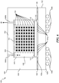
- Figure 3 is a cross-sectional view of another embodiment of the assembly 100 in accordance with the present invention.
- the first portion 131 of the TTS 130 has a sidewall 146 with a height (H 2 ) that extends to at least approximately the same elevation as the top of the uppermost second die 120
- the second portion 132 of the TTS 130 has a bottom 154 attached to the top of the sidewall 146.
- the second portion 132 accordingly does not have a separate sidewall pendent from the top 152.
- the second portion 132 can be attached to the first portion 131 by the adhesive 133.
- Figure 4A is a side cross-sectional view and Figure 4B is a top plan view of a semiconductor die assembly 400 at one stage of a manufacturing process in accordance with the present invention.
- Figure 4A shows the assembly 400 after an inner casing 430 has been attached to the first die 110.
- the inner casing 430 can include a first support 431 with a first interior surface 433, a second support 432 with a second interior surface 434, and a top 435 extending between the first and second supports 431 and 432.
- the inner casing 430 has a cavity 436 that is closed on the sides with the first and second supports 431 and 432, but open on the other two sides.
- the first and second supports 431 and 432 can be attached to the peripheral region 112 of the first die 110 with the adhesive 133.
- the top 435 of the inner casing 430 can also be attached to the top of the second die 120 by the adhesive 133.
- the inner casing 430 can have a footprint similar to the footprint of the first die 110.
- Figure 4C is a side cross-sectional view of the assembly 400 at a subsequent stage of manufacturing after the underfill material 160 has been deposited between the second dies 120 and between the first die 110 and the bottom second die 120.
- the underfill material can be distributed within the interstitial spaces by flowing the underfill material through the open sides of the inner casing 430 as shown by arrow F.
- the assembly 400 can be inclined at an angle such that gravity pulls the underfill material 160 through the interstitial spaces within the cavity 436.
- Figure 4D is a side cross-sectional view and Figure 4E is a top plan view of the assembly 400 at a subsequent stage of manufacturing.
- the assembly 400 further includes an outer casing 440 having a sidewall 442 with an inner surface 444 and a top 446 that together define a cavity 448.
- the inner surface 444 of the sidewall 442 has four sides such that the cavity 448 encloses the first die 110, the stack of second dies 120, and the inner casing 430.
- the outer casing 440 can be attached to the package support substrate 102 by the adhesive 148 and to the top 435 of the inner casing 430 by the adhesive 133.
- This embodiment provides a good thermal interface with the peripheral region 112 of the first die 110 as explained above and with the sides of the second dies 120 because the underfill material 160 can have a higher thermal conductivity than a void in within the casing.
- FIG. 5A is a cross-sectional view and Figure 5B is a top plan view of a semiconductor device assembly 500 ("assembly 500") not in accordance with the claimed invention.
- the assembly 500 includes a TTS 530 having a top 532, a sidewall 534 integrally formed with the top 532, and a cavity 538 defined by the top 532 and the sidewall 534.
- the TTS 530 is a single-piece casing formed from a material having a high thermal conductivity, such as copper or aluminum.
- the sidewall 534 can have an interior surface 535.
- the interior surface 535 can have four sides configured to be spaced apart from the stack 122 of second dies 120 such that a small gap exists between the second dies 120 and the interior surface 535 of the sidewall 534.
- the sidewall 534 can further include a foundation 536 attached to the package support substrate 102 by the adhesive 148 and a shoulder 537 attached to the peripheral region 112 of the first die 110 by the adhesive 133.
- the foundation 536 can be a footing that has an inner surface 539 spaced laterally outward from the peripheral region 112 of the first die 110.
- the TTS 530 can further include an inlet 540a and an outlet 540b.
- the inlet 540a can be a first passageway extending through a lower portion of the sidewall 534, and the outlet 540b can be a second passageway that extends through an upper portion of the sidewall 534.
- the inlet 540a and the outlet 540b can be laterally offset from each other, or in other embodiments they can be aligned with each other across the cavity 538.
- the inlet 540a and outlet 540b can extend through the sidewall at approximately the same elevation.
- the inlet 540a can be positioned relatively higher along the sidewall 534 than the outlet 540b.
- the underfill material 160 is injected (I) into the cavity 538 via the inlet 540a such that the underfill material 160 fills the interstitial spaces between the second dies 120 and between the first die and the bottom second die 120.
- the underfill material 160 can be injected into the cavity 538 until the underfill material 160 flows out of the outlet 540b (O).
- the inlet 540a and outlet 540b can be sealed by filling these passageways with the underfill material 160, or in other embodiments the exterior openings of the inlet 540a and outlet 540b can be capped with another material to seal the cavity 538 within the TTS 530.
- the TTS 530 provides a dam member that effectively contains the underfill material 160 while also providing coverage of a large surface area of the peripheral region 112 of the first die 110 by the shoulder 537 of the sidewall 534. Moreover, the underfill material 160 also contacts the sides of the second die 120 to also enhance the heat transfer laterally away from the second dies 120.
- FIG. 6 is a cross-sectional view of a semiconductor die assembly 600 ("assembly 600") not in accordance with the claimed invention.
- the assembly 600 can include a TTS 630 having a top 632 and a sidewall 634 having an interior surface 636.
- the top 632 and the sidewall 634 define a cavity 638 configured to receive the first die 110 and the stack 122 of second dies 120.
- the top 632 can be attached to the upper second die 120 by the adhesive 133, and the sidewall 634 can be attached to the package support substrate 102 by the adhesive 148.
- the embodiment of the sidewall 634 shown in Figure 6 does not contact the peripheral region 112 of the first die 110.
- the sidewall 634 can have a shoulder adhered to the peripheral region 112 of the first die 110 and a foundation adhered to the package support substrate 102 as shown by the shoulder 537 and foundation 536 of the sidewall 534 show in Figure 5A .
- the TTS 630 can further include an inlet 640a and an outlet 640b.
- the inlet 640a and outlet 640b are passageways that extend through the top 632 of the TTS 630.
- the inlet 640a and/or the outlet 640b can be passageways through the sidewall 634.
- the embodiment of the TTS 630 illustrated in Figure 6 is a single-piece casing in which the top 632 is formed integrally with the sidewall 634.
- the top 632 can be a separate component that is attached to the sidewall 634 by an adhesive, such as shown and described with respect to Figure 3 .
- the assembly 600 further includes a thermally conductive dielectric liquid 670 in the cavity 638.
- the dielectric liquid 670 can be injected into the cavity 638 (I) via the inlet 640a.
- the outlet 640b can accordingly provide a vent through which air or other matter can escape (O) from the cavity 638 as the dielectric liquid 670 is injected.
- the dielectric liquid 670 can be injected as a liquid and remain in the liquid state within the cavity 638, or it can be injected as a liquid and partially cured to a gel-like substance or fully cured to a solid.
- Suitable thermally conductive dielectric liquids 670 include, for example, paraffin fluid and DowthermTM manufactured by the Dow Chemical Company.
- Suitable DowthermTM heat transfer fluids include Dowtherm ATM, Dowtherm GTM, Dowtherm QTM and Dowtherm TTM, all of which are manufactured by the Dow Chemical Company.
- the dielectric liquid 670 should have a boiling point greater than the maximum operating temperature of the assembly 600 to avoid generating a gas in the cavity.
- the dielectric liquid 670 can be selected to cure to a solid or semi-solid material at ambient temperatures, but undergo a phase change to a liquid state at or near maximum operating temperatures to potentially enhance the heat transfer and provide a steady state operating temperature when maximum operating temperatures are reached.
- the dielectric liquid 670 can fill the interstitial spaces between the second dies 120 and between the first die 110 and the bottom second die 120 such that a separate underfill material is not necessarily required.
- an underfill material may be deposited between the second dies 120 and between the first die 110 and the bottom second die 120 before filling the cavity 638 with the dielectric liquid 670.
- the underfill material is generally desirable when the dielectric liquid 670 remains in the liquid state to provide structural support for the dies 110, 120. However, the underfill material can be eliminated when the dielectric liquid 670 cures to a sufficiently solid state.
- the dielectric liquid 670 contacts not only the peripheral region 112 of the first die 110, but also the second dies 120 to efficiently transfer heat to the TTS 630.
- This provides significantly more surface contact between a material with high thermal conductivity and the dies 110 and 120 compared to devices that use an underfill material and/or have voids between the casing and the dies 110 and 120.
- the cavity 638 is completely filled to prevent voids within the TTS 630, and the inlet 640a and outlet 640b are capped to seal the cavity 638.
- the embodiment of the assembly 600 is expected to provide highly efficient heat transfer from the first and second dies 110 and 120.
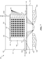
- Figure 7 is a cross-sectional view of another embodiment of the assembly 600 not in accordance with the claimed invention.
- the inlet 640a is a passageway extending through a lower portion of the sidewall 634 and the outlet 640b is a passageway extending through the top 632.
- This embodiment provides bottom up filling of the cavity 638, which is expected to mitigate the possible formation of air pockets within the cavity 638.
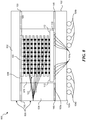
- FIG. 8 is a cross-sectional view illustrating another embodiment of the assembly 600 not in accordance with the claimed invention.
- the TTS 630 is a multi-piece casing having a top component 632 and a separate sidewall 634 that are attached to each other by the adhesive 133.
- the sidewall 634 can be attached to the package support substrate 102 by the adhesive 148, and then the space between the interior surface 636 of the sidewall 634 and the dies 110 and 120 can be filled with the dielectric liquid 670.
- the top 632 is then attached to the sidewall 634 and the upper second die 120 by the adhesive 133.
- the cavity 638 will have a small void caused by the thickness of the adhesives 133.
- the top 632 of the TTS 630 can be attached to the sidewall 634 in a vacuum.
- FIG. 9 is a cross-sectional view of a semiconductor die assembly 900 ("assembly 900") in accordance with another embodiment of the present invention.
- the embodiment illustrated in Figure 9 is similar to the embodiment of the assembly 100 illustrated in Figure 2F , and therefore like reference numbers refer to like components in Figures 1-9 .
- the TTS 130 can further include an inlet 910a and an outlet 910b in the second portion 132 of the TTS 130.
- the inlet 910a and outlet 910b are passageways that are exposed to the cavity 138 within the TTS 130.
- the assembly 900 further includes both the underfill material 160 and the dielectric liquid 670 in the cavity 138.
- the underfill material 160 can be deposited as described above with reference to Figure 2E .
- the dielectric liquid 670 can be injected into the cavity via the inlet 910a, and air or excess dielectric liquid 670 can pass out of the cavity 138 via the outlet 910b. After the cavity 138 has been filled with the dielectric liquid 670, the inlet 910a and outlet 910b can be capped or otherwise sealed to seal the cavity 138 from the external environment.
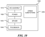
- the system 1000 can include a semiconductor die assembly 1010, a power source 1020, a driver 1030, a processor 1040, and/or other subsystems or components 1050.
- the semiconductor die assembly 1010 can include features generally similar to those of the stacked semiconductor die assemblies described above, and can therefore include multiple thermal paths with good coverage of the peripheral region 112 of the first die 110 that enhance heat dissipation.
- the resulting system 1000 can perform any of a wide variety of functions, such as memory storage, data processing, and/or other suitable functions.
- representative systems 1000 can include, without limitation, hand-held devices (e.g., mobile phones, tablets, digital readers, and digital audio players), computers, and appliances.
- Components of the system 1000 may be housed in a single unit or distributed over multiple, interconnected units (e.g., through a communications network).
- the components of the system 1000 can also include remote devices and any of a wide variety of computer readable media.
- the semiconductor die assemblies can be configured as other memory devices or other types of stacked die assemblies.
- the semiconductor die assemblies illustrated in Figures 1-9 include a plurality of first semiconductor dies arranged in a stack on the second semiconductor die. In other embodiments not all of which fall within the scope of the claimed invention, however, the semiconductor die assemblies can include one first semiconductor die stacked on one or more of the second semiconductor dies.
Landscapes
- Engineering & Computer Science (AREA)
- Cooling Or The Like Of Semiconductors Or Solid State Devices (AREA)
- Manufacturing & Machinery (AREA)
- Encapsulation Of And Coatings For Semiconductor Or Solid State Devices (AREA)
- Chemical & Material Sciences (AREA)
- Materials Engineering (AREA)
- Structures Or Materials For Encapsulating Or Coating Semiconductor Devices Or Solid State Devices (AREA)
Claims (15)
- Procédé de mise en boîtier d'un assemblage (100) de puces semi-conductrices ayant une première puce (110) et une pluralité de deuxièmes puces (120) agencées en un empilement (122) et fixées à la première puce, la première puce ayant une région périphérique (112) s'étendant latéralement vers l'extérieur depuis l'empilement de deuxièmes puces, le procédé comprenant :le positionnement d'au moins une partie d'une structure de transfert thermique (130) sur la région périphérique (112) de la première puce, la structure de transfert thermique comprenant un matériau thermoconducteur ;caractérisé par l'écoulement d'un matériau de sous-remplissage (160) entre les deuxièmes puces après le positionnement de la structure de transfert thermique sur la région périphérique de la première puce, le matériau de sous-remplissage ayant un cordon (162) s'étendant latéralement depuis l'empilement de deuxièmes puces, et l'extension latérale du matériau de sous-remplissage étant limitée par la structure de transfert thermique.
- Procédé de la revendication 1 dans lequel :la structure de transfert thermique comprend une première partie (131) ayant une assise (142) configurée pour s'étendre au moins autour d'une partie de la première puce et un épaulement (144) configuré pour être positionné par-dessus la région périphérique de la première puce ; etle positionnement d'au moins une partie de la structure de transfert thermique sur la région périphérique de la première puce comprend la fixation de l'assise à un substrat de support de boîtier et de l'épaulement à la région périphérique de la première puce avec un matériau d'interface thermique entre l'épaulement et la région périphérique de la première puce.
- Procédé de la revendication 1 dans lequel :la structure de transfert thermique comprend une première partie (131) ayant (a) une assise (142) configurée pour s'étendre au moins autour d'une partie de la première puce et être fixée à un substrat de support de boîtier et (b) un épaulement (144) configuré pour être fixé à une surface supérieure de la région périphérique ;le positionnement d'au moins une partie de la structure de transfert thermique sur la région périphérique de la première puce comprend la fixation de l'assise à un substrat de support de boîtier (102) et de l'épaulement à la région périphérique de la première puce avec un matériau d'interface thermique entre l'épaulement et la région périphérique de la première puce ; etle procédé comprend en outre la fixation d'une deuxième partie (132) de la structure de transfert thermique à la première partie de la structure de transfert thermique après l'écoulement du matériau de sous-remplissage, les première et deuxième parties de la structure de transfert thermique formant une enveloppe ayant une cavité dans laquelle la première puce et l'empilement de deuxièmes puces sont positionnés.
- Procédé de la revendication 3 dans lequel la première partie de la structure de transfert thermique comprend un élément faisant barrage et la deuxième partie de la structure de transfert thermique comprend un couvercle, et dans lequel le couvercle a un dessus et une paroi latérale pendante depuis le dessus, et la paroi latérale est fixée à l'élément faisant barrage.
- Procédé de la revendication 3 dans lequel la première partie de la structure de transfert thermique comprend une paroi latérale s'étendant jusqu'à une hauteur d'une deuxième puce la plus haute et la deuxième partie de la structure de transfert thermique comprend un dessus.
- Procédé de la revendication 1 dans lequel :la structure de transfert thermique comprend une paroi latérale (534), un dessus (532) formé d'une seule pièce avec la paroi latérale, une cavité (538) formée par la paroi latérale et le dessus, et une entrée (540a, 640a) ;la paroi latérale a une assise configurée pour entourer au moins une partie de la première puce et un épaulement configuré pour être positionné par-dessus la région périphérique de la première puce ;le positionnement de la structure de transfert thermique sur la région périphérique de la première puce comprend la fixation de l'assise à un substrat de support de boîtier et la fixation de l'épaulement à la région périphérique de la puce, l'empilement de deuxièmes puces étant dans la cavité ; etl'écoulement du matériau de sous-remplissage entre les deuxièmes puces comprend l'injection du matériau de sous-remplissage dans la cavité par l'entrée.
- Procédé de la revendication 6 dans lequel, soit l'entrée est un premier passage (540a) à travers une zone inférieure de la paroi latérale et la structure de transfert thermique comprend une sortie qui est un deuxième passage (540b) à travers une zone supérieure à la paroi latérale ; soit l'entrée est un premier passage (640a) à travers le dessus et la structure de transfert thermique comprend une sortie qui est un deuxième passage (640b) à travers le dessus.
- Procédé de la revendication 1 dans lequel :la structure de transfert thermique comprend une enveloppe interne ayant un premier support et un dessus s'étendant depuis le premier support ;le positionnement d'au moins une partie de la structure de transfert thermique sur la région périphérique de la première puce comprend la fixation du premier support à la région périphérique de la puce, l'empilement de deuxièmes puces étant sous le dessus de l'enveloppe ; etl'écoulement du matériau de sous-remplissage entre les deuxièmes puces comprend l'écoulement du matériau de sous-remplissage entre l'empilement de deuxièmes puces et l'enveloppe interne.
- Procédé de la revendication 8 dans lequel l'enveloppe interne comprend en outre un deuxième support et le dessus a une extrémité fixée au premier support et une autre extrémité fixée au deuxième support, et dans lequel le positionnement de la structure de transfert thermique sur la région périphérique de la première puce comprend la fixation des premier et deuxième supports à la région périphérique de la première puce.
- Procédé de la revendication 8, la structure de transfert thermique comprenant en outre une enveloppe externe ayant une cavité, et le procédé comportant en outre la fixation de l'enveloppe externe à un substrat de support de boîtier et l'enveloppe interne de telle sorte que l'enveloppe interne est reçue à l'intérieur de la cavité de l'enveloppe externe.
- Procédé de la revendication 1 dans lequel la structure de transfert thermique comprend une enveloppe métallique ayant une cavité, et dans lequel le positionnement d'au moins une partie de la structure de transfert thermique dans la région périphérique de la première puce comprend la fixation d'une partie inférieure de l'enveloppe métallique à la région périphérique de la première puce avec un matériau d'interface thermique de telle sorte que l'empilement de deuxièmes puces est dans la cavité de l'enveloppe métallique.
- Procédé de la revendication 11 dans lequel :l'enveloppe métallique comprend un anneau métallique et un couvercle métallique ;le positionnement d'au moins une partie de la structure de transfert thermique dans la région périphérique de la première puce comprend la fixation de l'anneau à la région périphérique ; etle procédé comprend en outre la fixation du couvercle métallique à l'anneau après l'écoulement du matériau de sous-remplissage de telle sorte que l'empilement de deuxièmes puces est enfermé à l'intérieur de l'anneau métallique et du couvercle métallique.
- Procédé de la revendication 11 dans lequel :l'enveloppe métallique comprend une paroi latérale métallique, un dessus métallique qui, conjointement avec la paroi latérale métallique, forme la cavité, et une entrée ;le positionnement d'au moins une partie de la structure de transfert thermique dans la région périphérique de la première puce comprend la fixation de la paroi latérale à la région périphérique ; etl'écoulement d'un matériau de sous-remplissage entre les deuxièmes puces comprend l'injection du matériau de sous-remplissage dans la cavité par l'entrée.
- Procédé de la revendication 1, comprenant en outre l'instillation d'un liquide diélectrique (670) à l'intérieur de l'enveloppe après l'écoulement du matériau de sous-remplissage, le liquide diélectrique étant thermoconducteur ; et
le durcissement au moins partiel du liquide diélectrique à l'intérieur de la cavité. - Procédé de la revendication 1 dans lequel :le positionnement d'au moins une partie d'une structure de transfert thermique dans la région périphérique de la première puce comprend le positionnement d'une première partie de la structure de transfert thermique ayant une première paroi latérale s'étendant depuis la région périphérique jusqu'à une hauteur à une altitude intermédiaire de l'empilement de deuxièmes puces ; etle procédé comprend en outre la fixation d'une deuxième partie de la structure de transfert thermique à la première partie de la structure de transfert thermique après l'écoulement du matériau de sous-remplissage, la deuxième partie comportant un couvercle ayant un dessus et une deuxième paroi latérale pendante depuis le dessus, et la deuxième paroi latérale étant configurée pour se fixer à la première paroi latérale à l'altitude intermédiaire.
Applications Claiming Priority (2)
| Application Number | Priority Date | Filing Date | Title |
|---|---|---|---|
| US14/330,805 US9691746B2 (en) | 2014-07-14 | 2014-07-14 | Methods of manufacturing stacked semiconductor die assemblies with high efficiency thermal paths |
| PCT/US2015/037621 WO2016010702A1 (fr) | 2014-07-14 | 2015-06-25 | Procédés de fabrication d'ensembles de puces de semi-conducteur empilées à chemins thermiques à haute efficacité |
Publications (3)
| Publication Number | Publication Date |
|---|---|
| EP3170200A1 EP3170200A1 (fr) | 2017-05-24 |
| EP3170200A4 EP3170200A4 (fr) | 2018-01-24 |
| EP3170200B1 true EP3170200B1 (fr) | 2020-01-15 |
Family
ID=55068167
Family Applications (1)
| Application Number | Title | Priority Date | Filing Date |
|---|---|---|---|
| EP15822244.8A Active EP3170200B1 (fr) | 2014-07-14 | 2015-06-25 | Procédés de fabrication d'ensembles de puces de semi-conducteur empilées à chemins thermiques à haute efficacité |
Country Status (7)
| Country | Link |
|---|---|
| US (5) | US9691746B2 (fr) |
| EP (1) | EP3170200B1 (fr) |
| JP (1) | JP6317028B2 (fr) |
| KR (1) | KR101996153B1 (fr) |
| CN (1) | CN106537588B (fr) |
| TW (1) | TWI588915B (fr) |
| WO (1) | WO2016010702A1 (fr) |
Families Citing this family (34)
| Publication number | Priority date | Publication date | Assignee | Title |
|---|---|---|---|---|
| US9735082B2 (en) | 2013-12-04 | 2017-08-15 | Taiwan Semiconductor Manufacturing Company, Ltd. | 3DIC packaging with hot spot thermal management features |
| US9691746B2 (en) | 2014-07-14 | 2017-06-27 | Micron Technology, Inc. | Methods of manufacturing stacked semiconductor die assemblies with high efficiency thermal paths |
| US10068181B1 (en) | 2015-04-27 | 2018-09-04 | Rigetti & Co, Inc. | Microwave integrated quantum circuits with cap wafer and methods for making the same |
| US11329026B2 (en) * | 2016-02-17 | 2022-05-10 | Micron Technology, Inc. | Apparatuses and methods for internal heat spreading for packaged semiconductor die |
| US10032695B2 (en) | 2016-02-19 | 2018-07-24 | Google Llc | Powermap optimized thermally aware 3D chip package |
| US9865570B1 (en) * | 2017-02-14 | 2018-01-09 | Globalfoundries Inc. | Integrated circuit package with thermally conductive pillar |
| US10199356B2 (en) * | 2017-02-24 | 2019-02-05 | Micron Technology, Inc. | Semiconductor device assembles with electrically functional heat transfer structures |
| US10096576B1 (en) | 2017-06-13 | 2018-10-09 | Micron Technology, Inc. | Semiconductor device assemblies with annular interposers |
| US10090282B1 (en) | 2017-06-13 | 2018-10-02 | Micron Technology, Inc. | Semiconductor device assemblies with lids including circuit elements |
| US11121301B1 (en) | 2017-06-19 | 2021-09-14 | Rigetti & Co, Inc. | Microwave integrated quantum circuits with cap wafers and their methods of manufacture |
| US11088062B2 (en) * | 2017-07-19 | 2021-08-10 | Intel Corporation | Method to enable 30 microns pitch EMIB or below |
| CN107256850B (zh) * | 2017-07-25 | 2023-03-31 | 厦门大学 | 一种内嵌金属微通道的转接板及其制备方法 |
| US10515867B2 (en) * | 2017-11-14 | 2019-12-24 | Taiwan Semiconductor Manufacturing Company Ltd. | Semiconductor structure and manufacturing method thereof |
| US10453820B2 (en) | 2018-02-07 | 2019-10-22 | Micron Technology, Inc. | Semiconductor assemblies using edge stacking and methods of manufacturing the same |
| US10971439B2 (en) | 2018-02-22 | 2021-04-06 | Hamilton Sundstrand Corporation | Ball grid array underfilling systems |
| US11094608B2 (en) | 2018-06-29 | 2021-08-17 | Taiwan Semiconductor Manufacturing Co., Ltd. | Heat dissipation structure including stacked chips surrounded by thermal interface material rings |
| CN110660759B (zh) * | 2018-06-29 | 2025-08-29 | 台湾积体电路制造股份有限公司 | 散热结构及制造散热结构的方法 |
| US11152333B2 (en) * | 2018-10-19 | 2021-10-19 | Micron Technology, Inc. | Semiconductor device packages with enhanced heat management and related systems |
| US10529637B1 (en) | 2018-10-31 | 2020-01-07 | Taiwan Semiconductor Manufacturing Company, Ltd. | Integrated circuit package and method of forming same |
| US11296051B2 (en) * | 2019-08-22 | 2022-04-05 | Taiwan Semiconductor Manufacturing Company, Ltd. | Semiconductor packages and forming method thereof |
| KR102562315B1 (ko) * | 2019-10-14 | 2023-08-01 | 삼성전자주식회사 | 반도체 패키지 |
| KR102643424B1 (ko) * | 2019-12-13 | 2024-03-06 | 삼성전자주식회사 | 반도체 패키지 |
| CN113035801A (zh) * | 2019-12-25 | 2021-06-25 | 台湾积体电路制造股份有限公司 | 存储器装置及其制造方法 |
| US11011449B1 (en) | 2020-02-27 | 2021-05-18 | Micron Technology, Inc. | Apparatus and method for dissipating heat in multiple semiconductor device modules |
| US11410961B2 (en) * | 2020-03-17 | 2022-08-09 | Micron Technology, Inc. | Methods and apparatus for temperature modification in bonding stacked microelectronic components and related substrates and assemblies |
| KR102792976B1 (ko) * | 2020-08-31 | 2025-04-11 | 에스케이하이닉스 주식회사 | 적층 반도체 칩을 포함하는 반도체 패키지 |
| CN113645759B (zh) * | 2021-08-09 | 2024-03-12 | 维沃移动通信有限公司 | 电路板组件、电子设备和电路板组件的加工方法 |
| US12400990B2 (en) | 2021-08-17 | 2025-08-26 | Samsung Electronics Co., Ltd. | Semiconductor package |
| US12211762B2 (en) * | 2021-09-13 | 2025-01-28 | Amkor Technology Singapore Holding Pte. Ltd. | Semiconductor devices and methods of manufacturing semiconductor devices |
| CN113966069B (zh) * | 2021-09-30 | 2024-07-05 | 华为数字能源技术有限公司 | 基板结构和终端设备 |
| US12593672B2 (en) * | 2022-02-17 | 2026-03-31 | Taiwan Semiconductor Manufacturing Co., Ltd. | Integrated circuit package and method |
| CN114551385B (zh) * | 2022-04-28 | 2022-09-13 | 之江实验室 | 含有微流道散热结构的三维堆叠封装结构及其封装方法 |
| US20250364360A1 (en) * | 2024-05-23 | 2025-11-27 | Micron Technology, Inc. | Method of forming stacked semiconductor devices with carbon nanofiber structures and associated systems and methods |
| US20250393222A1 (en) * | 2024-06-19 | 2025-12-25 | Micron Technology, Inc. | Semiconductor device heat spreader and method |
Citations (1)
| Publication number | Priority date | Publication date | Assignee | Title |
|---|---|---|---|---|
| JP2013069988A (ja) * | 2011-09-26 | 2013-04-18 | Toshiba Corp | 半導体装置とその製造方法 |
Family Cites Families (37)
| Publication number | Priority date | Publication date | Assignee | Title |
|---|---|---|---|---|
| US4323914A (en) | 1979-02-01 | 1982-04-06 | International Business Machines Corporation | Heat transfer structure for integrated circuit package |
| US5001548A (en) | 1989-03-13 | 1991-03-19 | Coriolis Corporation | Multi-chip module cooling |
| US5405808A (en) * | 1993-08-16 | 1995-04-11 | Lsi Logic Corporation | Fluid-filled and gas-filled semiconductor packages |
| KR100236016B1 (ko) * | 1996-12-16 | 1999-12-15 | 구자홍 | 적층형 반도체 패키지 및 그의 어셈블리 방법 |
| US6153929A (en) | 1998-08-21 | 2000-11-28 | Micron Technology, Inc. | Low profile multi-IC package connector |
| JP3459891B2 (ja) * | 1999-11-26 | 2003-10-27 | 埼玉日本電気株式会社 | Icパッケージの補強構造および方法 |
| TWI248842B (en) * | 2000-06-12 | 2006-02-11 | Hitachi Ltd | Semiconductor device and semiconductor module |
| US6686654B2 (en) | 2001-08-31 | 2004-02-03 | Micron Technology, Inc. | Multiple chip stack structure and cooling system |
| KR100446290B1 (ko) * | 2001-11-03 | 2004-09-01 | 삼성전자주식회사 | 댐을 포함하는 반도체 패키지 및 그 제조방법 |
| US20050224953A1 (en) | 2004-03-19 | 2005-10-13 | Lee Michael K L | Heat spreader lid cavity filled with cured molding compound |
| US7215018B2 (en) | 2004-04-13 | 2007-05-08 | Vertical Circuits, Inc. | Stacked die BGA or LGA component assembly |
| JP4983049B2 (ja) * | 2005-06-24 | 2012-07-25 | セイコーエプソン株式会社 | 半導体装置および電子機器 |
| WO2007053571A2 (fr) * | 2005-11-01 | 2007-05-10 | Techfilm, Llc | Materiau d'interface thermique avec garnissages conducteurs de chaleur a granulometrie multiple |
| US20070126103A1 (en) | 2005-12-01 | 2007-06-07 | Intel Corporation | Microelectronic 3-D package defining thermal through vias and method of making same |
| US20100117209A1 (en) | 2007-02-28 | 2010-05-13 | Bezama Raschid J | Multiple chips on a semiconductor chip with cooling means |
| JP4438006B2 (ja) * | 2007-03-30 | 2010-03-24 | Okiセミコンダクタ株式会社 | 半導体装置及び半導体装置の製造方法 |
| US7592697B2 (en) | 2007-08-27 | 2009-09-22 | Intel Corporation | Microelectronic package and method of cooling same |
| JP2009218432A (ja) * | 2008-03-11 | 2009-09-24 | Sharp Corp | 高周波モジュールおよび高周波モジュールの製造方法 |
| US7741156B2 (en) * | 2008-05-27 | 2010-06-22 | Stats Chippac, Ltd. | Semiconductor device and method of forming through vias with reflowed conductive material |
| US9142480B2 (en) * | 2008-08-15 | 2015-09-22 | Intel Corporation | Microelectronic package with high temperature thermal interface material |
| US8299633B2 (en) * | 2009-12-21 | 2012-10-30 | Advanced Micro Devices, Inc. | Semiconductor chip device with solder diffusion protection |
| JP2011216818A (ja) * | 2010-04-02 | 2011-10-27 | Elpida Memory Inc | 半導体装置の製造方法 |
| US8492911B2 (en) * | 2010-07-20 | 2013-07-23 | Lsi Corporation | Stacked interconnect heat sink |
| US8445918B2 (en) * | 2010-08-13 | 2013-05-21 | International Business Machines Corporation | Thermal enhancement for multi-layer semiconductor stacks |
| US9668811B2 (en) | 2010-11-16 | 2017-06-06 | Boston Scientific Scimed, Inc. | Minimally invasive access for renal nerve ablation |
| JP5861260B2 (ja) * | 2011-03-10 | 2016-02-16 | 日本電気株式会社 | 半導体装置の製造方法及び半導体装置 |
| JP2012253104A (ja) | 2011-05-31 | 2012-12-20 | Zycube:Kk | インターポーザを用いた積層モジュールの実装構造 |
| US8526186B2 (en) | 2011-07-11 | 2013-09-03 | Texas Instruments Incorporated | Electronic assembly including die on substrate with heat spreader having an open window on the die |
| US9269646B2 (en) * | 2011-11-14 | 2016-02-23 | Micron Technology, Inc. | Semiconductor die assemblies with enhanced thermal management and semiconductor devices including same |
| JP2013138177A (ja) * | 2011-11-28 | 2013-07-11 | Elpida Memory Inc | 半導体装置の製造方法 |
| KR101469485B1 (ko) * | 2012-08-13 | 2014-12-05 | 엘지디스플레이 주식회사 | 유기 발광 표시 장치 및 이의 제조 방법 |
| US20140291834A1 (en) * | 2013-03-27 | 2014-10-02 | Micron Technology, Inc. | Semiconductor devices and packages including conductive underfill material and related methods |
| CN108922959B (zh) | 2013-03-28 | 2022-07-29 | 日亚化学工业株式会社 | 发光装置、及使用发光装置的装置 |
| US9287240B2 (en) * | 2013-12-13 | 2016-03-15 | Micron Technology, Inc. | Stacked semiconductor die assemblies with thermal spacers and associated systems and methods |
| US9337119B2 (en) * | 2014-07-14 | 2016-05-10 | Micron Technology, Inc. | Stacked semiconductor die assemblies with high efficiency thermal paths and associated systems |
| US9443744B2 (en) * | 2014-07-14 | 2016-09-13 | Micron Technology, Inc. | Stacked semiconductor die assemblies with high efficiency thermal paths and associated methods |
| US9691746B2 (en) | 2014-07-14 | 2017-06-27 | Micron Technology, Inc. | Methods of manufacturing stacked semiconductor die assemblies with high efficiency thermal paths |
-
2014
- 2014-07-14 US US14/330,805 patent/US9691746B2/en active Active
-
2015
- 2015-06-25 CN CN201580037974.XA patent/CN106537588B/zh active Active
- 2015-06-25 KR KR1020177003527A patent/KR101996153B1/ko active Active
- 2015-06-25 JP JP2017501355A patent/JP6317028B2/ja active Active
- 2015-06-25 WO PCT/US2015/037621 patent/WO2016010702A1/fr not_active Ceased
- 2015-06-25 EP EP15822244.8A patent/EP3170200B1/fr active Active
- 2015-07-06 TW TW104121887A patent/TWI588915B/zh active
-
2017
- 2017-04-26 US US15/498,321 patent/US10163755B2/en active Active
-
2018
- 2018-06-27 US US16/020,567 patent/US20180308785A1/en not_active Abandoned
-
2021
- 2021-06-01 US US17/335,994 patent/US11776877B2/en active Active
-
2023
- 2023-08-23 US US18/454,703 patent/US20230395463A1/en active Pending
Patent Citations (1)
| Publication number | Priority date | Publication date | Assignee | Title |
|---|---|---|---|---|
| JP2013069988A (ja) * | 2011-09-26 | 2013-04-18 | Toshiba Corp | 半導体装置とその製造方法 |
Also Published As
| Publication number | Publication date |
|---|---|
| US9691746B2 (en) | 2017-06-27 |
| US20160013173A1 (en) | 2016-01-14 |
| WO2016010702A1 (fr) | 2016-01-21 |
| JP2017520932A (ja) | 2017-07-27 |
| US11776877B2 (en) | 2023-10-03 |
| US10163755B2 (en) | 2018-12-25 |
| TWI588915B (zh) | 2017-06-21 |
| US20220013434A1 (en) | 2022-01-13 |
| JP6317028B2 (ja) | 2018-04-25 |
| US20230395463A1 (en) | 2023-12-07 |
| KR20170029575A (ko) | 2017-03-15 |
| CN106537588B (zh) | 2019-10-11 |
| US20180308785A1 (en) | 2018-10-25 |
| KR101996153B1 (ko) | 2019-07-03 |
| EP3170200A1 (fr) | 2017-05-24 |
| EP3170200A4 (fr) | 2018-01-24 |
| CN106537588A (zh) | 2017-03-22 |
| US20170229439A1 (en) | 2017-08-10 |
| TW201606886A (zh) | 2016-02-16 |
Similar Documents
| Publication | Publication Date | Title |
|---|---|---|
| US20230395463A1 (en) | Methods of manufacturing stacked semiconductor die assemblies with high efficiency thermal paths | |
| EP3170198B1 (fr) | Ensembles de puces de semi-conducteur empilées à chemins thermiques à haute efficacité, et systèmes associés | |
| EP3170201B1 (fr) | Ensembles de puces de semi-conducteur empilées à chemins thermiques à haute efficacité | |
| US10424495B2 (en) | Stacked semiconductor die assemblies with high efficiency thermal paths and molded underfill |
Legal Events
| Date | Code | Title | Description |
|---|---|---|---|
| STAA | Information on the status of an ep patent application or granted ep patent |
Free format text: STATUS: THE INTERNATIONAL PUBLICATION HAS BEEN MADE |
|
| PUAI | Public reference made under article 153(3) epc to a published international application that has entered the european phase |
Free format text: ORIGINAL CODE: 0009012 |
|
| STAA | Information on the status of an ep patent application or granted ep patent |
Free format text: STATUS: REQUEST FOR EXAMINATION WAS MADE |
|
| 17P | Request for examination filed |
Effective date: 20170116 |
|
| AK | Designated contracting states |
Kind code of ref document: A1 Designated state(s): AL AT BE BG CH CY CZ DE DK EE ES FI FR GB GR HR HU IE IS IT LI LT LU LV MC MK MT NL NO PL PT RO RS SE SI SK SM TR |
|
| AX | Request for extension of the european patent |
Extension state: BA ME |
|
| DAV | Request for validation of the european patent (deleted) | ||
| DAX | Request for extension of the european patent (deleted) | ||
| A4 | Supplementary search report drawn up and despatched |
Effective date: 20180102 |
|
| RIC1 | Information provided on ipc code assigned before grant |
Ipc: H01L 23/48 20060101ALI20171219BHEP Ipc: H01L 23/04 20060101ALN20171219BHEP Ipc: H01L 23/367 20060101ALN20171219BHEP Ipc: H01L 23/28 20060101ALI20171219BHEP Ipc: H01L 25/065 20060101AFI20171219BHEP |
|
| STAA | Information on the status of an ep patent application or granted ep patent |
Free format text: STATUS: EXAMINATION IS IN PROGRESS |
|
| 17Q | First examination report despatched |
Effective date: 20180904 |
|
| GRAP | Despatch of communication of intention to grant a patent |
Free format text: ORIGINAL CODE: EPIDOSNIGR1 |
|
| STAA | Information on the status of an ep patent application or granted ep patent |
Free format text: STATUS: GRANT OF PATENT IS INTENDED |
|
| RIC1 | Information provided on ipc code assigned before grant |
Ipc: H01L 23/367 20060101ALN20190617BHEP Ipc: H01L 23/28 20060101ALI20190617BHEP Ipc: H01L 23/48 20060101ALI20190617BHEP Ipc: H01L 23/04 20060101ALN20190617BHEP Ipc: H01L 25/065 20060101AFI20190617BHEP |
|
| RIC1 | Information provided on ipc code assigned before grant |
Ipc: H01L 23/04 20060101ALN20190625BHEP Ipc: H01L 23/48 20060101ALI20190625BHEP Ipc: H01L 25/065 20060101AFI20190625BHEP Ipc: H01L 23/367 20060101ALN20190625BHEP Ipc: H01L 23/28 20060101ALI20190625BHEP |
|
| INTG | Intention to grant announced |
Effective date: 20190710 |
|
| GRAJ | Information related to disapproval of communication of intention to grant by the applicant or resumption of examination proceedings by the epo deleted |
Free format text: ORIGINAL CODE: EPIDOSDIGR1 |
|
| STAA | Information on the status of an ep patent application or granted ep patent |
Free format text: STATUS: EXAMINATION IS IN PROGRESS |
|
| GRAR | Information related to intention to grant a patent recorded |
Free format text: ORIGINAL CODE: EPIDOSNIGR71 |
|
| GRAS | Grant fee paid |
Free format text: ORIGINAL CODE: EPIDOSNIGR3 |
|
| STAA | Information on the status of an ep patent application or granted ep patent |
Free format text: STATUS: GRANT OF PATENT IS INTENDED |
|
| GRAA | (expected) grant |
Free format text: ORIGINAL CODE: 0009210 |
|
| STAA | Information on the status of an ep patent application or granted ep patent |
Free format text: STATUS: THE PATENT HAS BEEN GRANTED |
|
| INTC | Intention to grant announced (deleted) | ||
| RIC1 | Information provided on ipc code assigned before grant |
Ipc: H01L 23/28 20060101ALI20191202BHEP Ipc: H01L 23/367 20060101ALN20191202BHEP Ipc: H01L 23/04 20060101ALN20191202BHEP Ipc: H01L 23/48 20060101ALI20191202BHEP Ipc: H01L 25/065 20060101AFI20191202BHEP |
|
| AK | Designated contracting states |
Kind code of ref document: B1 Designated state(s): AL AT BE BG CH CY CZ DE DK EE ES FI FR GB GR HR HU IE IS IT LI LT LU LV MC MK MT NL NO PL PT RO RS SE SI SK SM TR |
|
| INTG | Intention to grant announced |
Effective date: 20191210 |
|
| REG | Reference to a national code |
Ref country code: CH Ref legal event code: EP Ref country code: GB Ref legal event code: FG4D |
|
| REG | Reference to a national code |
Ref country code: IE Ref legal event code: FG4D |
|
| REG | Reference to a national code |
Ref country code: DE Ref legal event code: R096 Ref document number: 602015045739 Country of ref document: DE |
|
| REG | Reference to a national code |
Ref country code: AT Ref legal event code: REF Ref document number: 1225909 Country of ref document: AT Kind code of ref document: T Effective date: 20200215 |
|
| REG | Reference to a national code |
Ref country code: NL Ref legal event code: MP Effective date: 20200115 |
|
| REG | Reference to a national code |
Ref country code: LT Ref legal event code: MG4D |
|
| PG25 | Lapsed in a contracting state [announced via postgrant information from national office to epo] |
Ref country code: PT Free format text: LAPSE BECAUSE OF FAILURE TO SUBMIT A TRANSLATION OF THE DESCRIPTION OR TO PAY THE FEE WITHIN THE PRESCRIBED TIME-LIMIT Effective date: 20200607 Ref country code: NO Free format text: LAPSE BECAUSE OF FAILURE TO SUBMIT A TRANSLATION OF THE DESCRIPTION OR TO PAY THE FEE WITHIN THE PRESCRIBED TIME-LIMIT Effective date: 20200415 Ref country code: RS Free format text: LAPSE BECAUSE OF FAILURE TO SUBMIT A TRANSLATION OF THE DESCRIPTION OR TO PAY THE FEE WITHIN THE PRESCRIBED TIME-LIMIT Effective date: 20200115 Ref country code: FI Free format text: LAPSE BECAUSE OF FAILURE TO SUBMIT A TRANSLATION OF THE DESCRIPTION OR TO PAY THE FEE WITHIN THE PRESCRIBED TIME-LIMIT Effective date: 20200115 Ref country code: NL Free format text: LAPSE BECAUSE OF FAILURE TO SUBMIT A TRANSLATION OF THE DESCRIPTION OR TO PAY THE FEE WITHIN THE PRESCRIBED TIME-LIMIT Effective date: 20200115 |
|
| PG25 | Lapsed in a contracting state [announced via postgrant information from national office to epo] |
Ref country code: GR Free format text: LAPSE BECAUSE OF FAILURE TO SUBMIT A TRANSLATION OF THE DESCRIPTION OR TO PAY THE FEE WITHIN THE PRESCRIBED TIME-LIMIT Effective date: 20200416 Ref country code: HR Free format text: LAPSE BECAUSE OF FAILURE TO SUBMIT A TRANSLATION OF THE DESCRIPTION OR TO PAY THE FEE WITHIN THE PRESCRIBED TIME-LIMIT Effective date: 20200115 Ref country code: BG Free format text: LAPSE BECAUSE OF FAILURE TO SUBMIT A TRANSLATION OF THE DESCRIPTION OR TO PAY THE FEE WITHIN THE PRESCRIBED TIME-LIMIT Effective date: 20200415 Ref country code: LV Free format text: LAPSE BECAUSE OF FAILURE TO SUBMIT A TRANSLATION OF THE DESCRIPTION OR TO PAY THE FEE WITHIN THE PRESCRIBED TIME-LIMIT Effective date: 20200115 Ref country code: SE Free format text: LAPSE BECAUSE OF FAILURE TO SUBMIT A TRANSLATION OF THE DESCRIPTION OR TO PAY THE FEE WITHIN THE PRESCRIBED TIME-LIMIT Effective date: 20200115 Ref country code: IS Free format text: LAPSE BECAUSE OF FAILURE TO SUBMIT A TRANSLATION OF THE DESCRIPTION OR TO PAY THE FEE WITHIN THE PRESCRIBED TIME-LIMIT Effective date: 20200515 |
|
| REG | Reference to a national code |
Ref country code: DE Ref legal event code: R097 Ref document number: 602015045739 Country of ref document: DE |
|
| PG25 | Lapsed in a contracting state [announced via postgrant information from national office to epo] |
Ref country code: CZ Free format text: LAPSE BECAUSE OF FAILURE TO SUBMIT A TRANSLATION OF THE DESCRIPTION OR TO PAY THE FEE WITHIN THE PRESCRIBED TIME-LIMIT Effective date: 20200115 Ref country code: RO Free format text: LAPSE BECAUSE OF FAILURE TO SUBMIT A TRANSLATION OF THE DESCRIPTION OR TO PAY THE FEE WITHIN THE PRESCRIBED TIME-LIMIT Effective date: 20200115 Ref country code: SK Free format text: LAPSE BECAUSE OF FAILURE TO SUBMIT A TRANSLATION OF THE DESCRIPTION OR TO PAY THE FEE WITHIN THE PRESCRIBED TIME-LIMIT Effective date: 20200115 Ref country code: DK Free format text: LAPSE BECAUSE OF FAILURE TO SUBMIT A TRANSLATION OF THE DESCRIPTION OR TO PAY THE FEE WITHIN THE PRESCRIBED TIME-LIMIT Effective date: 20200115 Ref country code: LT Free format text: LAPSE BECAUSE OF FAILURE TO SUBMIT A TRANSLATION OF THE DESCRIPTION OR TO PAY THE FEE WITHIN THE PRESCRIBED TIME-LIMIT Effective date: 20200115 Ref country code: ES Free format text: LAPSE BECAUSE OF FAILURE TO SUBMIT A TRANSLATION OF THE DESCRIPTION OR TO PAY THE FEE WITHIN THE PRESCRIBED TIME-LIMIT Effective date: 20200115 Ref country code: SM Free format text: LAPSE BECAUSE OF FAILURE TO SUBMIT A TRANSLATION OF THE DESCRIPTION OR TO PAY THE FEE WITHIN THE PRESCRIBED TIME-LIMIT Effective date: 20200115 Ref country code: EE Free format text: LAPSE BECAUSE OF FAILURE TO SUBMIT A TRANSLATION OF THE DESCRIPTION OR TO PAY THE FEE WITHIN THE PRESCRIBED TIME-LIMIT Effective date: 20200115 |
|
| REG | Reference to a national code |
Ref country code: AT Ref legal event code: MK05 Ref document number: 1225909 Country of ref document: AT Kind code of ref document: T Effective date: 20200115 |
|
| PLBE | No opposition filed within time limit |
Free format text: ORIGINAL CODE: 0009261 |
|
| STAA | Information on the status of an ep patent application or granted ep patent |
Free format text: STATUS: NO OPPOSITION FILED WITHIN TIME LIMIT |
|
| 26N | No opposition filed |
Effective date: 20201016 |
|
| PG25 | Lapsed in a contracting state [announced via postgrant information from national office to epo] |
Ref country code: AT Free format text: LAPSE BECAUSE OF FAILURE TO SUBMIT A TRANSLATION OF THE DESCRIPTION OR TO PAY THE FEE WITHIN THE PRESCRIBED TIME-LIMIT Effective date: 20200115 Ref country code: MC Free format text: LAPSE BECAUSE OF FAILURE TO SUBMIT A TRANSLATION OF THE DESCRIPTION OR TO PAY THE FEE WITHIN THE PRESCRIBED TIME-LIMIT Effective date: 20200115 Ref country code: IT Free format text: LAPSE BECAUSE OF FAILURE TO SUBMIT A TRANSLATION OF THE DESCRIPTION OR TO PAY THE FEE WITHIN THE PRESCRIBED TIME-LIMIT Effective date: 20200115 |
|
| REG | Reference to a national code |
Ref country code: CH Ref legal event code: PL |
|
| PG25 | Lapsed in a contracting state [announced via postgrant information from national office to epo] |
Ref country code: PL Free format text: LAPSE BECAUSE OF FAILURE TO SUBMIT A TRANSLATION OF THE DESCRIPTION OR TO PAY THE FEE WITHIN THE PRESCRIBED TIME-LIMIT Effective date: 20200115 Ref country code: SI Free format text: LAPSE BECAUSE OF FAILURE TO SUBMIT A TRANSLATION OF THE DESCRIPTION OR TO PAY THE FEE WITHIN THE PRESCRIBED TIME-LIMIT Effective date: 20200115 |
|
| GBPC | Gb: european patent ceased through non-payment of renewal fee |
Effective date: 20200625 |
|
| PG25 | Lapsed in a contracting state [announced via postgrant information from national office to epo] |
Ref country code: LU Free format text: LAPSE BECAUSE OF NON-PAYMENT OF DUE FEES Effective date: 20200625 |
|
| REG | Reference to a national code |
Ref country code: BE Ref legal event code: MM Effective date: 20200630 |
|
| PG25 | Lapsed in a contracting state [announced via postgrant information from national office to epo] |
Ref country code: GB Free format text: LAPSE BECAUSE OF NON-PAYMENT OF DUE FEES Effective date: 20200625 Ref country code: LI Free format text: LAPSE BECAUSE OF NON-PAYMENT OF DUE FEES Effective date: 20200630 Ref country code: FR Free format text: LAPSE BECAUSE OF NON-PAYMENT OF DUE FEES Effective date: 20200630 Ref country code: CH Free format text: LAPSE BECAUSE OF NON-PAYMENT OF DUE FEES Effective date: 20200630 Ref country code: IE Free format text: LAPSE BECAUSE OF NON-PAYMENT OF DUE FEES Effective date: 20200625 |
|
| PG25 | Lapsed in a contracting state [announced via postgrant information from national office to epo] |
Ref country code: BE Free format text: LAPSE BECAUSE OF NON-PAYMENT OF DUE FEES Effective date: 20200630 |
|
| PG25 | Lapsed in a contracting state [announced via postgrant information from national office to epo] |
Ref country code: TR Free format text: LAPSE BECAUSE OF FAILURE TO SUBMIT A TRANSLATION OF THE DESCRIPTION OR TO PAY THE FEE WITHIN THE PRESCRIBED TIME-LIMIT Effective date: 20200115 Ref country code: MT Free format text: LAPSE BECAUSE OF FAILURE TO SUBMIT A TRANSLATION OF THE DESCRIPTION OR TO PAY THE FEE WITHIN THE PRESCRIBED TIME-LIMIT Effective date: 20200115 Ref country code: CY Free format text: LAPSE BECAUSE OF FAILURE TO SUBMIT A TRANSLATION OF THE DESCRIPTION OR TO PAY THE FEE WITHIN THE PRESCRIBED TIME-LIMIT Effective date: 20200115 |
|
| PG25 | Lapsed in a contracting state [announced via postgrant information from national office to epo] |
Ref country code: MK Free format text: LAPSE BECAUSE OF FAILURE TO SUBMIT A TRANSLATION OF THE DESCRIPTION OR TO PAY THE FEE WITHIN THE PRESCRIBED TIME-LIMIT Effective date: 20200115 Ref country code: AL Free format text: LAPSE BECAUSE OF FAILURE TO SUBMIT A TRANSLATION OF THE DESCRIPTION OR TO PAY THE FEE WITHIN THE PRESCRIBED TIME-LIMIT Effective date: 20200115 |
|
| REG | Reference to a national code |
Ref country code: DE Ref legal event code: R079 Ref document number: 602015045739 Country of ref document: DE Free format text: PREVIOUS MAIN CLASS: H01L0025065000 Ipc: H10D0080300000 |
|
| PGFP | Annual fee paid to national office [announced via postgrant information from national office to epo] |
Ref country code: DE Payment date: 20250626 Year of fee payment: 11 |