EP3174185A1 - Stromversorgungsmodul und verfahren zum verpacken des stromversorgungsmoduls - Google Patents
Stromversorgungsmodul und verfahren zum verpacken des stromversorgungsmoduls Download PDFInfo
- Publication number
- EP3174185A1 EP3174185A1 EP16184829.6A EP16184829A EP3174185A1 EP 3174185 A1 EP3174185 A1 EP 3174185A1 EP 16184829 A EP16184829 A EP 16184829A EP 3174185 A1 EP3174185 A1 EP 3174185A1
- Authority
- EP
- European Patent Office
- Prior art keywords
- electrical winding
- lead frame
- power supply
- supply module
- bare chip
- Prior art date
- Legal status (The legal status is an assumption and is not a legal conclusion. Google has not performed a legal analysis and makes no representation as to the accuracy of the status listed.)
- Granted
Links
Images


Classifications
-
- H—ELECTRICITY
- H10—SEMICONDUCTOR DEVICES; ELECTRIC SOLID-STATE DEVICES NOT OTHERWISE PROVIDED FOR
- H10W—GENERIC PACKAGES, INTERCONNECTIONS, CONNECTORS OR OTHER CONSTRUCTIONAL DETAILS OF DEVICES COVERED BY CLASS H10
- H10W70/00—Package substrates; Interposers; Redistribution layers [RDL]
- H10W70/40—Leadframes
-
- H—ELECTRICITY
- H10—SEMICONDUCTOR DEVICES; ELECTRIC SOLID-STATE DEVICES NOT OTHERWISE PROVIDED FOR
- H10W—GENERIC PACKAGES, INTERCONNECTIONS, CONNECTORS OR OTHER CONSTRUCTIONAL DETAILS OF DEVICES COVERED BY CLASS H10
- H10W72/00—Interconnections or connectors in packages
- H10W72/60—Strap connectors, e.g. thick copper clips for grounding of power devices
-
- H—ELECTRICITY
- H10—SEMICONDUCTOR DEVICES; ELECTRIC SOLID-STATE DEVICES NOT OTHERWISE PROVIDED FOR
- H10W—GENERIC PACKAGES, INTERCONNECTIONS, CONNECTORS OR OTHER CONSTRUCTIONAL DETAILS OF DEVICES COVERED BY CLASS H10
- H10W90/00—Package configurations
-
- H—ELECTRICITY
- H10—SEMICONDUCTOR DEVICES; ELECTRIC SOLID-STATE DEVICES NOT OTHERWISE PROVIDED FOR
- H10W—GENERIC PACKAGES, INTERCONNECTIONS, CONNECTORS OR OTHER CONSTRUCTIONAL DETAILS OF DEVICES COVERED BY CLASS H10
- H10W72/00—Interconnections or connectors in packages
- H10W72/071—Connecting or disconnecting
- H10W72/073—Connecting or disconnecting of die-attach connectors
- H10W72/07331—Connecting techniques
- H10W72/07336—Soldering or alloying
-
- H—ELECTRICITY
- H10—SEMICONDUCTOR DEVICES; ELECTRIC SOLID-STATE DEVICES NOT OTHERWISE PROVIDED FOR
- H10W—GENERIC PACKAGES, INTERCONNECTIONS, CONNECTORS OR OTHER CONSTRUCTIONAL DETAILS OF DEVICES COVERED BY CLASS H10
- H10W72/00—Interconnections or connectors in packages
- H10W72/071—Connecting or disconnecting
- H10W72/076—Connecting or disconnecting of strap connectors
- H10W72/07631—Techniques
- H10W72/07636—Soldering or alloying
-
- H—ELECTRICITY
- H10—SEMICONDUCTOR DEVICES; ELECTRIC SOLID-STATE DEVICES NOT OTHERWISE PROVIDED FOR
- H10W—GENERIC PACKAGES, INTERCONNECTIONS, CONNECTORS OR OTHER CONSTRUCTIONAL DETAILS OF DEVICES COVERED BY CLASS H10
- H10W72/00—Interconnections or connectors in packages
- H10W72/071—Connecting or disconnecting
- H10W72/076—Connecting or disconnecting of strap connectors
- H10W72/07631—Techniques
- H10W72/07637—Techniques using a polymer adhesive, e.g. an adhesive based on silicone or epoxy
-
- H—ELECTRICITY
- H10—SEMICONDUCTOR DEVICES; ELECTRIC SOLID-STATE DEVICES NOT OTHERWISE PROVIDED FOR
- H10W—GENERIC PACKAGES, INTERCONNECTIONS, CONNECTORS OR OTHER CONSTRUCTIONAL DETAILS OF DEVICES COVERED BY CLASS H10
- H10W72/00—Interconnections or connectors in packages
- H10W72/071—Connecting or disconnecting
- H10W72/076—Connecting or disconnecting of strap connectors
- H10W72/07651—Connecting or disconnecting of strap connectors characterised by changes in properties of the strap connectors during connecting
- H10W72/07653—Connecting or disconnecting of strap connectors characterised by changes in properties of the strap connectors during connecting changes in shapes
-
- H—ELECTRICITY
- H10—SEMICONDUCTOR DEVICES; ELECTRIC SOLID-STATE DEVICES NOT OTHERWISE PROVIDED FOR
- H10W—GENERIC PACKAGES, INTERCONNECTIONS, CONNECTORS OR OTHER CONSTRUCTIONAL DETAILS OF DEVICES COVERED BY CLASS H10
- H10W72/00—Interconnections or connectors in packages
- H10W72/50—Bond wires
- H10W72/541—Dispositions of bond wires
- H10W72/5449—Dispositions of bond wires not being orthogonal to a side surface of the chip, e.g. fan-out arrangements
-
- H—ELECTRICITY
- H10—SEMICONDUCTOR DEVICES; ELECTRIC SOLID-STATE DEVICES NOT OTHERWISE PROVIDED FOR
- H10W—GENERIC PACKAGES, INTERCONNECTIONS, CONNECTORS OR OTHER CONSTRUCTIONAL DETAILS OF DEVICES COVERED BY CLASS H10
- H10W72/00—Interconnections or connectors in packages
- H10W72/50—Bond wires
- H10W72/551—Materials of bond wires
- H10W72/552—Materials of bond wires comprising metals or metalloids, e.g. silver
- H10W72/5522—Materials of bond wires comprising metals or metalloids, e.g. silver comprising gold [Au]
-
- H—ELECTRICITY
- H10—SEMICONDUCTOR DEVICES; ELECTRIC SOLID-STATE DEVICES NOT OTHERWISE PROVIDED FOR
- H10W—GENERIC PACKAGES, INTERCONNECTIONS, CONNECTORS OR OTHER CONSTRUCTIONAL DETAILS OF DEVICES COVERED BY CLASS H10
- H10W72/00—Interconnections or connectors in packages
- H10W72/60—Strap connectors, e.g. thick copper clips for grounding of power devices
- H10W72/651—Materials of strap connectors
- H10W72/652—Materials of strap connectors comprising metals or metalloids, e.g. silver
-
- H—ELECTRICITY
- H10—SEMICONDUCTOR DEVICES; ELECTRIC SOLID-STATE DEVICES NOT OTHERWISE PROVIDED FOR
- H10W—GENERIC PACKAGES, INTERCONNECTIONS, CONNECTORS OR OTHER CONSTRUCTIONAL DETAILS OF DEVICES COVERED BY CLASS H10
- H10W72/00—Interconnections or connectors in packages
- H10W72/851—Dispositions of multiple connectors or interconnections
- H10W72/853—On the same surface
- H10W72/871—Bond wires and strap connectors
-
- H—ELECTRICITY
- H10—SEMICONDUCTOR DEVICES; ELECTRIC SOLID-STATE DEVICES NOT OTHERWISE PROVIDED FOR
- H10W—GENERIC PACKAGES, INTERCONNECTIONS, CONNECTORS OR OTHER CONSTRUCTIONAL DETAILS OF DEVICES COVERED BY CLASS H10
- H10W90/00—Package configurations
- H10W90/701—Package configurations characterised by the relative positions of pads or connectors relative to package parts
- H10W90/751—Package configurations characterised by the relative positions of pads or connectors relative to package parts of bond wires
- H10W90/756—Package configurations characterised by the relative positions of pads or connectors relative to package parts of bond wires between a chip and a stacked lead frame, conducting package substrate or heat sink
-
- H—ELECTRICITY
- H10—SEMICONDUCTOR DEVICES; ELECTRIC SOLID-STATE DEVICES NOT OTHERWISE PROVIDED FOR
- H10W—GENERIC PACKAGES, INTERCONNECTIONS, CONNECTORS OR OTHER CONSTRUCTIONAL DETAILS OF DEVICES COVERED BY CLASS H10
- H10W90/00—Package configurations
- H10W90/701—Package configurations characterised by the relative positions of pads or connectors relative to package parts
- H10W90/761—Package configurations characterised by the relative positions of pads or connectors relative to package parts of strap connectors
- H10W90/763—Package configurations characterised by the relative positions of pads or connectors relative to package parts of strap connectors between laterally-adjacent chips
-
- H—ELECTRICITY
- H10—SEMICONDUCTOR DEVICES; ELECTRIC SOLID-STATE DEVICES NOT OTHERWISE PROVIDED FOR
- H10W—GENERIC PACKAGES, INTERCONNECTIONS, CONNECTORS OR OTHER CONSTRUCTIONAL DETAILS OF DEVICES COVERED BY CLASS H10
- H10W90/00—Package configurations
- H10W90/701—Package configurations characterised by the relative positions of pads or connectors relative to package parts
- H10W90/761—Package configurations characterised by the relative positions of pads or connectors relative to package parts of strap connectors
- H10W90/766—Package configurations characterised by the relative positions of pads or connectors relative to package parts of strap connectors between a chip and a stacked lead frame, conducting package substrate or heat sink
Definitions
- Embodiments of the present invention relate to electronic technologies, and in particular, to a power supply module and a method for packaging a power supply module.
- Main components of a power supply module include a power switch, an integrated circuit (Integrated circuit, IC for short), and passive devices.
- the passive devices include a magnetic device, a resistor, and a capacitor.
- the magnetic device may be an inductor.
- a commonly used power switch is a metal-oxide semiconductor field- effect transistor (MOSFET Metallic Oxide Semiconductor Field Effect Transistor, MOSFET for short) or an insulated gate bipolar transistor (Insulated Gate Bipolar Transistor, IGBT for short), and the IC may be a driver chip, a PWM control chip, or a combination of a driver chip and a PWM control chip.
- MOSFET MOSFET
- IC integrated circuit
- passive devices a structure into which a MOSFET, an IC, and passive devices are integrated.
- a PCB or another lead frame uses a gold wire or copper wire bonding interconnection manner.
- the MOSFET is controlled or driven by the IC to perform pulse width modulation on an input power supply, and after filtering is performed by an inductor and a capacitor, a voltage required by a load is output.
- a magnetic device in a power supply module is generally a surface mount magnetic device or a winding magnetic device including a magnetic core material.
- the surface mount magnetic device has a small inductance and cannot meet requirements on power density and power supply efficiency, so that reliability of the power supply module deteriorates.
- An inductance of the winding magnetic device including the magnetic core material is large; however, a winding magnetic device that has been packaged is used in the power supply module, leading to a high risk of welding joint cracking, a high failure probability, and low reliability.
- Embodiments of the present invention provide a power supply module and a method for packaging a power supply module, so as to lower a failure probability of a winding magnetic device in the power supply module and improve reliability of the power supply module.
- an embodiment of the present invention provides a power supply module, including:
- an embodiment of the present invention further provides a method for packaging a power supply module, including:
- At least one magnetic device in a power supply module is a discrete magnetic device obtained by assembling a magnetic core and an electrical winding in a process of packaging the power supply module instead of a packaged magnetic device independently packaged.
- One end of the electrical winding of the discrete magnetic device is electrically connected to a semiconductor bare chip directly and does not need to be electrically connected to the semiconductor bare chip by means of a lead frame.
- the magnetic device in the power supply module provided in the embodiments of the present invention is a discrete magnetic device, which reduces mechanical stress of an electrical connection between the magnetic device and the lead frame, improves heat dissipation performance, and lowers a failure probability of the magnetic device.
- the one end of the electrical winding of the discrete magnetic device is electrically connected to the semiconductor bare chip directly, which further reduces connection wires between internal devices of the power supply module, lowers impedance, and improves efficiency of the power supply module.
- a power supply module provided in an embodiment of the present invention includes a lead frame, an integrated circuit, passive devices, and at least one semiconductor bare chip.
- the semiconductor bare chip may be a MOSFET, or an IGBT, or a combination of an IGBT and a MOSFET.
- the power supply module provided in the embodiment of the present invention may be mounted on a PCB motherboard by means of the lead frame.
- At least one magnetic device in the passive devices is a discrete magnetic device including a magnetic core and an electrical winding.
- the power supply module provided in the embodiment of the present invention has at least one discrete magnetic device, and the discrete magnetic device is a magnetic device obtained by assembling a magnetic core and an electrical winding in a process of packaging the power supply module, is not exteriorly packaged, and is not an independently packaged magnetic device.
- a material of the electrical winding may be metal, such as gold, aluminum, or copper, and may be of any proper width and thickness.
- One end of the electrical winding of the discrete magnetic device is electrically connected to the lead frame, so that the one end of the electrical winding is electrically connected to the integrated circuit and the passive devices except all magnetic devices by means of the lead frame.
- the other end of the electrical winding of the discrete magnetic device is electrically connected to the semiconductor bare chip directly and does not need to be electrically connected to the semiconductor bare chip by means of the lead frame.
- the electrical winding may be electrically connected to the lead frame and the semiconductor bare chip in a welding manner, a bonding manner, or an adhering manner with a conductive adhesive, which is not limited to these three manners.
- the electrical winding is an aluminum strip; and the one end of the electrical winding is electrically connected to the lead frame in a bonding manner or an adhering manner, and the other end of the electrical winding is electrically connected to the semiconductor bare chip directly in a bonding manner or an adhering manner. Electrical connection is performed in a bonding or adhering manner, which can reduce connection wires between internal devices of the power supply module, reduce parasitic parameters, lower losses, and improve power supply efficiency.
- the integrated circuit is connected to the semiconductor bare chip and the passive devices by means of the lead frame.
- the power supply module may include two semiconductor bare chips, and a source of one semiconductor bare chip is electrically connected to a gate of the other semiconductor bare chip; and the other end of the electrical winding is electrically connected to the source of the one semiconductor bare chip directly, and the other end of the electrical winding is further electrically connected to the gate of the other semiconductor bare chip directly.
- At least one magnetic device is a discrete magnetic device obtained by assembling a magnetic core and an electrical winding in a process of packaging the power supply module instead of a packaged magnetic device independently packaged.
- One end of the electrical winding of the discrete magnetic device is electrically connected to a semiconductor bare chip directly and does not need to be electrically connected to the semiconductor bare chip by means of a lead frame.
- the magnetic device in the power supply module provided in the embodiment of the present invention is a discrete magnetic device, which reduces mechanical stress of an electrical connection between the magnetic device and the lead frame, improves heat dissipation performance, and lowers a failure probability of the magnetic device.
- the one end of the electrical winding of the discrete magnetic device is electrically connected to the semiconductor bare chip directly, which further reduces connection wires between internal devices of the power supply module, lowers impedance, and improves efficiency of the power supply module.
- FIG. 1 is a schematic structural diagram of a power supply module according to an embodiment of the present invention.
- the power supply module provided in this embodiment includes a magnetic device, and the magnetic device is a discrete magnetic device obtained by assembling two half magnetic cores and an electrical winding.
- a magnetic core of the discrete magnetic device includes two half magnetic cores disposed in a coupling manner, and the electrical winding is disposed in space between the two coupled half magnetic cores.
- a protruding part such as a protruding cylinder is disposed in a center of a surface of each half magnetic core, and the two half magnetic cores are disposed in a coupling manner by means of the central protruding parts.
- the discrete magnetic device in this embodiment includes a half magnetic core 21, a half magnetic core 22, and an electrical winding 23.
- a protruding part is disposed in a center of each of the half magnetic core 21 and the half magnetic core 22, and the half magnetic core 21 and the half magnetic core 22 are disposed in a coupling manner by means of the central protruding parts.
- the electrical winding 23 is disposed in space between the half magnetic core 21 and the half magnetic core 22 that are coupled together. Therefore, the electrical winding 23 is wrapped by the half magnetic core 21 and the half magnetic core 22.
- One end 231 of the electrical winding 23 is electrically connected to a lead frame 1, that is, the one end 231 of the electrical winding 23 is electrically connected to an integrated circuit 5 and passive devices except the magnetic device by means of the lead frame 1.
- the power supply module includes two cascaded semiconductor bare chips, and a source of a semiconductor bare chip 3 is electrically connected to a gate of a semiconductor bare chip 4.
- the other end 232 of the electrical winding 23 is electrically connected to the semiconductor bare chip 3 and the semiconductor bare chip 4 directly, that is, the other end of the electrical winding 23 is electrically connected to the source of the semiconductor bare chip 3 directly, and is further electrically connected to the gate of the semiconductor bare chip 4 directly.
- the semiconductor bare chip 3 and the semiconductor bare chip 4 are further electrically connected to the integrated circuit 5 by means of the lead frame.
- the discrete magnetic device in this embodiment is not manufactured independently, but obtained by assembly in a module packaging process.
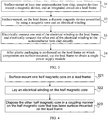
- a half magnetic core with a central protruding part is first mounted on the lead frame, and a surface, of the half magnetic core, without a protruding part is disposed on the lead frame, and then the electrical winding is laid on the half magnetic core. Then, the one end of the electrical winding is connected to the lead frame, and the other end is electrically connected to the semiconductor bare chip directly. Then, a central protruding part of the other half magnetic core is coupled to the protruding part of the half magnetic core that has been mounted, to close a magnetic circuit of the electrical winding.
- FIG. 2 is a schematic structural diagram of another power supply module according to an embodiment of the present invention.
- a discrete magnetic device is obtained by assembling a magnetic core and an electrical winding, and the electrical winding is wound around an exterior of the magnetic core.
- an electrical winding 62 is wound around an exterior of a magnetic core 61, and the magnetic core wound with the electrical winding 62 forms a discrete magnetic device by assembly.
- One end 621 of the electrical winding 62 is electrically connected to a lead frame 1, that is, the one end 621 of the electrical winding 62 is electrically connected to an integrated circuit 5 and passive devices except the magnetic device by means of the lead frame 1.
- the power supply module includes two cascaded semiconductor bare chips, and a source of a semiconductor bare chip 3 is electrically connected to a gate of a semiconductor bare chip 4.
- the other end 622 of the electrical winding 62 is electrically connected to the semiconductor bare chip 3 and the semiconductor bare chip 4 directly, that is, the other end 622 of the electrical winding 62 is electrically connected to the source of the semiconductor bare chip 3 directly, and is further electrically connected to the gate of the semiconductor bare chip 4 directly.
- the other end 622 of the electrical winding 62 is connected to a top portion of a semiconductor bare chip, and a bottom portion of the semiconductor bare chip is connected to the lead frame by using soldering tin, and is connected to an electrical winding at a bottom portion of the magnetic core 61.
- the discrete magnetic device in this embodiment is not manufactured independently, but obtained by assembly in a module packaging process.
- a magnetic core of which an exterior is wound with the electrical winding is first mounted on the lead frame, and then one exposed end of the electrical winding is connected to the lead frame, and the other exposed end is electrically connected to the semiconductor bare chip directly.
- the electrical winding may be a metal strip-shaped wire with one or more turns.
- the turns are connected to each other in series or in parallel, and one end of each turn is electrically connected to the lead frame in a mechanical press-fit manner.
- the electrical winding is an aluminum strip; and the one end of the electrical winding is electrically connected to the lead frame in a bonding manner or an adhering manner, and the other end of the electrical winding is electrically connected to the semiconductor bare chip in a bonding manner or an adhering manner directly.
- the semiconductor bare chip is a vertical semiconductor device.
- a lead frame may be obtained by using a stamping technique known in the art, or may be a predetermined graph obtained by using an etched conductive plate, or may be obtained with reference to the stamping technique and an etching technique. Therefore, a structure of the lead frame in the embodiments may be a continuous or discontinuous metal structure.
- the structure of the lead frame includes any proper material, may be of any proper form and thickness, and further includes a metal coating layer on the lead frame, such as a silver coating layer, a nickel-gold coating layer, or a nickel-palladium-gold coating layer.
- a body material of the lead frame includes copper, aluminum and aluminum alloy, ferronickel, and the like.
- the lead frame is initially one of many units of a lead frame array that are connected together by using a tie rod.
- the lead frame array may be cut or punched so that packaging is performed separately.
- the structure of the lead frame may have multiple die pad areas (DAP) in which a die attach pad Die Attach Pad may be formed, and a lead may be coplanar with or not coplanar with a surface of a die attach pad DAP.
- DAP die pad areas
- a module packaging material used for packaging the power supply module may include a proper material, such as a multifunctional cross-linked epoxy resin composite material.
- the module packaging material is softened from a fixed material cake form at a high temperature to a colloidal state in which solids and liquids coexist, transferred and injected into a mould to shape with a lead frame placed in the mould, and solidified and shaped after a crosslinking reaction.
- FIG. 3 is a flowchart of a method for packaging a power supply module according to an embodiment of the present invention.
- the packaging method provided in this embodiment includes:
- the discrete magnetic device is a magnetic device obtained by assembling the magnetic core and the electrical winding in a process of packaging the power supply module, is not exteriorly packaged, and is not an independently packaged magnetic device.
- a material of the foregoing electrical winding may be metal, such as gold, aluminum, or copper, and may be of any proper width and thickness.
- Step 33 Electrically connect one end of the electrical winding to the lead frame, and electrically connect the other end of the electrical winding to the semiconductor bare chip directly.
- One end of the electrical winding of the discrete magnetic device is electrically connected to the lead frame, so that the one end of the electrical winding is electrically connected to the integrated circuit and the passive devices except the magnetic device by means of the lead frame.
- the other end of the electrical winding of the discrete magnetic device is electrically connected to the semiconductor bare chip directly and does not need to be electrically connected to the semiconductor bare chip by means of the lead frame.
- the electrical winding may be electrically connected to the lead frame and the semiconductor bare chip in a welding manner, a bonding manner, or an adhering manner with a conductive adhesive, which is not limited to these three manners.
- the electrical winding is an aluminum strip; and the one end of the electrical winding is electrically connected to the lead frame in a bonding manner or an adhering manner, and the other end of the electrical winding is electrically connected to the semiconductor bare chip directly in a bonding manner or an adhering manner. Electrical connection is performed in a bonding or adhering manner, which can reduce connection wires between internal devices of the power supply module, reduce parasitic parameters, lower losses, and improve power supply efficiency.
- Step 34 After plastic packaging is performed on the lead frame on which components are surface-mounted, cut the lead frame to obtain a single power supply module.
- the electrical winding may be a metal strip-shaped wire with one or more turns.
- the turns are connected to each other in series or in parallel, and one end of each turn is electrically connected to the lead frame in a mechanical press-fit manner.
- the semiconductor bare chip is a vertical semiconductor device.
- a discrete magnetic device obtained by assembling a magnetic core and an electrical winding is surface-mounted on a lead frame instead of surface-mounting an independently packaged magnetic device on the lead frame.
- One end of the electrical winding of the discrete magnetic device is electrically connected to a semiconductor bare chip directly rather than electrically connected to the semiconductor bare chip by means of the lead frame.
- the magnetic device in the power supply module provided in the embodiment of the present invention is a discrete magnetic device, which reduces mechanical stress of an electrical connection between the magnetic device and the lead frame and improves heat dissipation performance.
- the one end of the electrical winding of the discrete magnetic device is electrically connected to the semiconductor bare chip directly, which further reduces connection wires between internal devices of the power supply module, lowers impedance, and improves efficiency of the power supply module.
- FIG. 4 is a flowchart of step 32 in FIG. 3 .
- the packaging method provided in this embodiment is a method for packaging the power supply module provided in FIG. 1 .
- step 32 includes:
- a specific packaging process is as follows: preparing the lead frame, coating a solder paste on the lead frame, surface-mounting the semiconductor bare chip and the passive devices except the magnetic device on the lead frame, and performing washing; then, performing, on the lead frame, dispensing for mounting the integrated circuit and the half magnetic core, and surface-mounting the integrated circuit and the half magnetic core with a central protruding part on the lead frame, where the central protruding part of the half magnetic core faces upwards; filling the bottom portions of the integrated circuit and the half magnetic core with a filling adhesive and solidifying the bottom portions; laying the electrical winding on the half magnetic core, and respectively connecting the two ends of the electrical winding to the lead frame and the semiconductor bare chip in a bonding manner; connecting the integrated circuit and the semiconductor bare chip in a bonding manner; performing dispensing on the central protruding part of the half magnetic core that has been surface-mounted on the lead frame, and surface-mounting a central protruding part of the other half magnetic core on the central protru
- the present invention may also use a magnetic core of which an exterior is wound with the electrical winding to assemble the discrete magnetic device.
- step 32 may be specifically surface-mounting, on the lead frame, the magnetic core of which the exterior is wound with the electrical winding.
- a specific packaging process is as follows: preparing the lead frame, coating a solder paste on the lead frame, surface-mounting the semiconductor bare chip and the passive devices except the magnetic device on the lead frame, and performing washing; then, performing, on the lead frame, dispensing for mounting the integrated circuit and the magnetic core, and surface-mounting the integrated circuit and the magnetic core of which the exterior is wound with the electrical winding on the lead frame; respectively connecting the two ends of the electrical winding to the lead frame and the semiconductor bare chip in a bonding manner; connecting the integrated circuit and the semiconductor bare chip in a bonding manner; and after plastic packaging is performed on the lead frame on which components are surface-mounted, cutting the lead frame to obtain a single power supply module.
- the foregoing packaging method may be a method for packaging the power supply module provided in FIG. 2 .
- a discrete magnetic device obtained by assembling a magnetic core and an electrical winding is surface-mounted on a lead frame instead of surface-mounting an independently packaged magnetic device on the lead frame.
- One end of the electrical winding of the discrete magnetic device is electrically connected to a semiconductor bare chip directly and does not need to be electrically connected to the semiconductor bare chip by means of the lead frame.
- the magnetic device in a power supply module provided in the embodiments of the present invention is a discrete magnetic device, which reduces mechanical stress of an electrical connection between the magnetic device and the lead frame and improves heat dissipation performance. Meanwhile, the one end of the electrical winding of the discrete magnetic device is electrically connected to the semiconductor bare chip directly, which further reduces connection wires between internal devices of the power supply module, lowers impedance, and improves efficiency of the power supply module.
Landscapes
- Dc-Dc Converters (AREA)
- Coils Or Transformers For Communication (AREA)
- Structures Or Materials For Encapsulating Or Coating Semiconductor Devices Or Solid State Devices (AREA)
- Manufacturing Cores, Coils, And Magnets (AREA)
Applications Claiming Priority (3)
| Application Number | Priority Date | Filing Date | Title |
|---|---|---|---|
| CN201210268316.XA CN102790513B (zh) | 2012-07-30 | 2012-07-30 | 电源模块和电源模块的封装方法 |
| PCT/CN2013/073950 WO2014019384A1 (zh) | 2012-07-30 | 2013-04-09 | 电源模块和电源模块的封装方法 |
| EP13824822.4A EP2802064B1 (de) | 2012-07-30 | 2013-04-09 | Leistungsmodul und verkapselungsverfahren dafür |
Related Parent Applications (2)
| Application Number | Title | Priority Date | Filing Date |
|---|---|---|---|
| EP13824822.4A Division EP2802064B1 (de) | 2012-07-30 | 2013-04-09 | Leistungsmodul und verkapselungsverfahren dafür |
| EP13824822.4A Division-Into EP2802064B1 (de) | 2012-07-30 | 2013-04-09 | Leistungsmodul und verkapselungsverfahren dafür |
Publications (2)
| Publication Number | Publication Date |
|---|---|
| EP3174185A1 true EP3174185A1 (de) | 2017-05-31 |
| EP3174185B1 EP3174185B1 (de) | 2020-09-16 |
Family
ID=47155833
Family Applications (2)
| Application Number | Title | Priority Date | Filing Date |
|---|---|---|---|
| EP16184829.6A Active EP3174185B1 (de) | 2012-07-30 | 2013-04-09 | Stromversorgungsmodul und verfahren zum verpacken des stromversorgungsmoduls |
| EP13824822.4A Active EP2802064B1 (de) | 2012-07-30 | 2013-04-09 | Leistungsmodul und verkapselungsverfahren dafür |
Family Applications After (1)
| Application Number | Title | Priority Date | Filing Date |
|---|---|---|---|
| EP13824822.4A Active EP2802064B1 (de) | 2012-07-30 | 2013-04-09 | Leistungsmodul und verkapselungsverfahren dafür |
Country Status (4)
| Country | Link |
|---|---|
| EP (2) | EP3174185B1 (de) |
| CN (1) | CN102790513B (de) |
| ES (2) | ES2836188T3 (de) |
| WO (1) | WO2014019384A1 (de) |
Cited By (1)
| Publication number | Priority date | Publication date | Assignee | Title |
|---|---|---|---|---|
| EP4156252A4 (de) * | 2020-05-19 | 2023-08-09 | Mitsubishi Electric Corporation | Halbleitermodul |
Families Citing this family (13)
| Publication number | Priority date | Publication date | Assignee | Title |
|---|---|---|---|---|
| CN102790513B (zh) * | 2012-07-30 | 2014-12-10 | 华为技术有限公司 | 电源模块和电源模块的封装方法 |
| CN203691210U (zh) * | 2013-12-25 | 2014-07-02 | 中兴通讯股份有限公司 | 一种集成封装电源 |
| US12058814B2 (en) | 2016-03-03 | 2024-08-06 | Delta Electronics (Shanghai) Co., Ltd. | Power module and manufacturing method thereof |
| CN107154301B (zh) * | 2016-03-03 | 2018-12-25 | 台达电子企业管理(上海)有限公司 | 磁性组件 |
| US11277067B2 (en) | 2016-03-03 | 2022-03-15 | Delta Electronics, Inc. | Power module and manufacturing method thereof |
| US9768099B1 (en) | 2016-05-06 | 2017-09-19 | Infineon Technologies Americas Corp. | IC package with integrated inductor |
| CN108022899B (zh) * | 2016-10-28 | 2020-02-11 | 台达电子工业股份有限公司 | 具有引线部件的电源模块及其制造方法 |
| CN108633247A (zh) * | 2018-05-04 | 2018-10-09 | 北京星原丰泰电子技术股份有限公司 | 砖类模块电源磁性元件装配机及装配方法 |
| US11127524B2 (en) | 2018-12-14 | 2021-09-21 | Hong Kong Applied Science and Technology Research Institute Company Limited | Power converter |
| WO2020118707A1 (zh) * | 2018-12-14 | 2020-06-18 | 华为技术有限公司 | 电源模块及其制备方法、通信设备 |
| US10964628B2 (en) | 2019-02-21 | 2021-03-30 | Infineon Technologies Ag | Clip frame assembly, semiconductor package having a lead frame and a clip frame, and method of manufacture |
| US11515244B2 (en) | 2019-02-21 | 2022-11-29 | Infineon Technologies Ag | Clip frame assembly, semiconductor package having a lead frame and a clip frame, and method of manufacture |
| CN116631989A (zh) * | 2019-06-14 | 2023-08-22 | 华为数字能源技术有限公司 | 一种封装模块及金属板 |
Citations (6)
| Publication number | Priority date | Publication date | Assignee | Title |
|---|---|---|---|---|
| US5839184A (en) * | 1997-07-10 | 1998-11-24 | Vlsi Technology, Inc. | Method for creating on-package inductors for use with integrated circuits |
| EP1091404A1 (de) * | 1999-10-06 | 2001-04-11 | Lucent Technologies Inc. | Multifunktions-Leiterrahmen und Gehäuse für eine integrierte Schaltung mit demselben |
| US20050285262A1 (en) * | 2002-09-10 | 2005-12-29 | James Knapp | Semiconductor device with wire bond inductor and method |
| US20070074386A1 (en) * | 2005-10-05 | 2007-04-05 | Lotfi Ashraf W | Method of forming a power module with a magnetic device having a conductive clip |
| WO2008011459A2 (en) * | 2006-07-19 | 2008-01-24 | Texas Intruments Incorporated | Power semiconductor devices having integrated inductor |
| CN102171825A (zh) * | 2011-04-29 | 2011-08-31 | 华为技术有限公司 | 电源模块及其封装集成方法 |
Family Cites Families (9)
| Publication number | Priority date | Publication date | Assignee | Title |
|---|---|---|---|---|
| JP2004103837A (ja) * | 2002-09-10 | 2004-04-02 | Nec Tokin Corp | 薄型dc/dcコンバータ |
| JP2008301594A (ja) * | 2007-05-30 | 2008-12-11 | Panasonic Corp | 電源ユニット |
| US20090057822A1 (en) * | 2007-09-05 | 2009-03-05 | Yenting Wen | Semiconductor component and method of manufacture |
| JP2010251582A (ja) * | 2009-04-17 | 2010-11-04 | Sanken Electric Co Ltd | Dc−dcコンバータ |
| TWI581384B (zh) * | 2009-12-07 | 2017-05-01 | 英特希爾美國公司 | 堆疊式電子電感封裝組件及其製造技術 |
| US10111333B2 (en) * | 2010-03-16 | 2018-10-23 | Intersil Americas Inc. | Molded power-supply module with bridge inductor over other components |
| US8569861B2 (en) * | 2010-12-22 | 2013-10-29 | Analog Devices, Inc. | Vertically integrated systems |
| CN102157394A (zh) * | 2011-03-22 | 2011-08-17 | 南通富士通微电子股份有限公司 | 高密度系统级封装方法 |
| CN102790513B (zh) * | 2012-07-30 | 2014-12-10 | 华为技术有限公司 | 电源模块和电源模块的封装方法 |
-
2012
- 2012-07-30 CN CN201210268316.XA patent/CN102790513B/zh active Active
-
2013
- 2013-04-09 ES ES16184829T patent/ES2836188T3/es active Active
- 2013-04-09 ES ES13824822.4T patent/ES2613004T3/es active Active
- 2013-04-09 EP EP16184829.6A patent/EP3174185B1/de active Active
- 2013-04-09 WO PCT/CN2013/073950 patent/WO2014019384A1/zh not_active Ceased
- 2013-04-09 EP EP13824822.4A patent/EP2802064B1/de active Active
Patent Citations (7)
| Publication number | Priority date | Publication date | Assignee | Title |
|---|---|---|---|---|
| US5839184A (en) * | 1997-07-10 | 1998-11-24 | Vlsi Technology, Inc. | Method for creating on-package inductors for use with integrated circuits |
| EP1091404A1 (de) * | 1999-10-06 | 2001-04-11 | Lucent Technologies Inc. | Multifunktions-Leiterrahmen und Gehäuse für eine integrierte Schaltung mit demselben |
| US20050285262A1 (en) * | 2002-09-10 | 2005-12-29 | James Knapp | Semiconductor device with wire bond inductor and method |
| US20070074386A1 (en) * | 2005-10-05 | 2007-04-05 | Lotfi Ashraf W | Method of forming a power module with a magnetic device having a conductive clip |
| WO2008011459A2 (en) * | 2006-07-19 | 2008-01-24 | Texas Intruments Incorporated | Power semiconductor devices having integrated inductor |
| CN102171825A (zh) * | 2011-04-29 | 2011-08-31 | 华为技术有限公司 | 电源模块及其封装集成方法 |
| EP2482312A2 (de) * | 2011-04-29 | 2012-08-01 | Huawei Technologies Co., Ltd. | Stromversorgungsmodul sowie verpackungs- und integrationsverfahren dafür |
Cited By (2)
| Publication number | Priority date | Publication date | Assignee | Title |
|---|---|---|---|---|
| EP4156252A4 (de) * | 2020-05-19 | 2023-08-09 | Mitsubishi Electric Corporation | Halbleitermodul |
| US12412813B2 (en) | 2020-05-19 | 2025-09-09 | Mitsubishi Electric Corporation | Semiconductor module |
Also Published As
| Publication number | Publication date |
|---|---|
| EP2802064A4 (de) | 2015-06-03 |
| EP2802064B1 (de) | 2016-11-09 |
| ES2836188T3 (es) | 2021-06-24 |
| CN102790513A (zh) | 2012-11-21 |
| ES2613004T3 (es) | 2017-05-19 |
| CN102790513B (zh) | 2014-12-10 |
| EP3174185B1 (de) | 2020-09-16 |
| WO2014019384A1 (zh) | 2014-02-06 |
| EP2802064A1 (de) | 2014-11-12 |
Similar Documents
| Publication | Publication Date | Title |
|---|---|---|
| EP3174185A1 (de) | Stromversorgungsmodul und verfahren zum verpacken des stromversorgungsmoduls | |
| US8153473B2 (en) | Module having a stacked passive element and method of forming the same | |
| US9054086B2 (en) | Module having a stacked passive element and method of forming the same | |
| US10389241B2 (en) | Power supply converter and method for manufacturing the same | |
| US8987877B2 (en) | Semiconductor device | |
| US9734944B2 (en) | Electronic package structure comprising a magnetic body and an inductive element and method for making the same | |
| US9852928B2 (en) | Semiconductor packages and modules with integrated ferrite material | |
| US20120273932A1 (en) | Power supply module and packaging and integrating method thereof | |
| US20120200281A1 (en) | Three-Dimensional Power Supply Module Having Reduced Switch Node Ringing | |
| US8582317B2 (en) | Method for manufacturing a semiconductor component and structure therefor | |
| US8063472B2 (en) | Semiconductor package with stacked dice for a buck converter | |
| US20110260314A1 (en) | Die package and corresponding method for realizing a double side cooling of a die package | |
| CN106298722A (zh) | 一种大电流功率半导体器件的封装结构及制造方法 | |
| CN107527899B (zh) | 功率组件、功率组件的制造方法及氮化镓智能功率模块 | |
| TW200810069A (en) | Dual side cooling integrated power device package and module and methods of manufacture | |
| CN114080652B (zh) | 表面安装的磁性组件模块 | |
| KR101629470B1 (ko) | 전력용 반도체 모듈의 조립방법 및 이를 이용하여 제조된 전력용 반도체 모듈 | |
| CN102163562B (zh) | 一种功率半导体管芯的安装方法和同步降压转换器 | |
| JP2004048084A (ja) | 半導体パワーモジュール | |
| CN106601694A (zh) | 堆叠结构及其制造方法 | |
| CN223501872U (zh) | 一种功率模块引线框架及功率模块 | |
| CN212209419U (zh) | 全集成电源一体成型器件及变换器 | |
| EP4432348A1 (de) | Leistungshalbleitergehäuse mit einem passiven elektronischen bauelement und verfahren zu seiner herstellung | |
| CN103579217B (zh) | 一种超小封装的电源模块及其封装方法 | |
| CN119542331A (zh) | 半导体结构及其制备方法 |
Legal Events
| Date | Code | Title | Description |
|---|---|---|---|
| PUAI | Public reference made under article 153(3) epc to a published international application that has entered the european phase |
Free format text: ORIGINAL CODE: 0009012 |
|
| STAA | Information on the status of an ep patent application or granted ep patent |
Free format text: STATUS: REQUEST FOR EXAMINATION WAS MADE |
|
| 17P | Request for examination filed |
Effective date: 20160819 |
|
| AC | Divisional application: reference to earlier application |
Ref document number: 2802064 Country of ref document: EP Kind code of ref document: P |
|
| AK | Designated contracting states |
Kind code of ref document: A1 Designated state(s): AL AT BE BG CH CY CZ DE DK EE ES FI FR GB GR HR HU IE IS IT LI LT LU LV MC MK MT NL NO PL PT RO RS SE SI SK SM TR |
|
| STAA | Information on the status of an ep patent application or granted ep patent |
Free format text: STATUS: EXAMINATION IS IN PROGRESS |
|
| 17Q | First examination report despatched |
Effective date: 20180329 |
|
| GRAP | Despatch of communication of intention to grant a patent |
Free format text: ORIGINAL CODE: EPIDOSNIGR1 |
|
| STAA | Information on the status of an ep patent application or granted ep patent |
Free format text: STATUS: GRANT OF PATENT IS INTENDED |
|
| INTG | Intention to grant announced |
Effective date: 20200515 |
|
| GRAS | Grant fee paid |
Free format text: ORIGINAL CODE: EPIDOSNIGR3 |
|
| GRAA | (expected) grant |
Free format text: ORIGINAL CODE: 0009210 |
|
| STAA | Information on the status of an ep patent application or granted ep patent |
Free format text: STATUS: THE PATENT HAS BEEN GRANTED |
|
| AC | Divisional application: reference to earlier application |
Ref document number: 2802064 Country of ref document: EP Kind code of ref document: P |
|
| AK | Designated contracting states |
Kind code of ref document: B1 Designated state(s): AL AT BE BG CH CY CZ DE DK EE ES FI FR GB GR HR HU IE IS IT LI LT LU LV MC MK MT NL NO PL PT RO RS SE SI SK SM TR |
|
| REG | Reference to a national code |
Ref country code: GB Ref legal event code: FG4D |
|
| REG | Reference to a national code |
Ref country code: CH Ref legal event code: EP |
|
| REG | Reference to a national code |
Ref country code: DE Ref legal event code: R096 Ref document number: 602013072677 Country of ref document: DE |
|
| REG | Reference to a national code |
Ref country code: IE Ref legal event code: FG4D |
|
| REG | Reference to a national code |
Ref country code: AT Ref legal event code: REF Ref document number: 1315039 Country of ref document: AT Kind code of ref document: T Effective date: 20201015 |
|
| REG | Reference to a national code |
Ref country code: FI Ref legal event code: FGE |
|
| REG | Reference to a national code |
Ref country code: NL Ref legal event code: FP |
|
| PG25 | Lapsed in a contracting state [announced via postgrant information from national office to epo] |
Ref country code: HR Free format text: LAPSE BECAUSE OF FAILURE TO SUBMIT A TRANSLATION OF THE DESCRIPTION OR TO PAY THE FEE WITHIN THE PRESCRIBED TIME-LIMIT Effective date: 20200916 Ref country code: SE Free format text: LAPSE BECAUSE OF FAILURE TO SUBMIT A TRANSLATION OF THE DESCRIPTION OR TO PAY THE FEE WITHIN THE PRESCRIBED TIME-LIMIT Effective date: 20200916 Ref country code: NO Free format text: LAPSE BECAUSE OF FAILURE TO SUBMIT A TRANSLATION OF THE DESCRIPTION OR TO PAY THE FEE WITHIN THE PRESCRIBED TIME-LIMIT Effective date: 20201216 Ref country code: GR Free format text: LAPSE BECAUSE OF FAILURE TO SUBMIT A TRANSLATION OF THE DESCRIPTION OR TO PAY THE FEE WITHIN THE PRESCRIBED TIME-LIMIT Effective date: 20201217 Ref country code: BG Free format text: LAPSE BECAUSE OF FAILURE TO SUBMIT A TRANSLATION OF THE DESCRIPTION OR TO PAY THE FEE WITHIN THE PRESCRIBED TIME-LIMIT Effective date: 20201216 |
|
| REG | Reference to a national code |
Ref country code: AT Ref legal event code: MK05 Ref document number: 1315039 Country of ref document: AT Kind code of ref document: T Effective date: 20200916 |
|
| PG25 | Lapsed in a contracting state [announced via postgrant information from national office to epo] |
Ref country code: RS Free format text: LAPSE BECAUSE OF FAILURE TO SUBMIT A TRANSLATION OF THE DESCRIPTION OR TO PAY THE FEE WITHIN THE PRESCRIBED TIME-LIMIT Effective date: 20200916 Ref country code: LV Free format text: LAPSE BECAUSE OF FAILURE TO SUBMIT A TRANSLATION OF THE DESCRIPTION OR TO PAY THE FEE WITHIN THE PRESCRIBED TIME-LIMIT Effective date: 20200916 |
|
| REG | Reference to a national code |
Ref country code: LT Ref legal event code: MG4D |
|
| PG25 | Lapsed in a contracting state [announced via postgrant information from national office to epo] |
Ref country code: EE Free format text: LAPSE BECAUSE OF FAILURE TO SUBMIT A TRANSLATION OF THE DESCRIPTION OR TO PAY THE FEE WITHIN THE PRESCRIBED TIME-LIMIT Effective date: 20200916 Ref country code: CZ Free format text: LAPSE BECAUSE OF FAILURE TO SUBMIT A TRANSLATION OF THE DESCRIPTION OR TO PAY THE FEE WITHIN THE PRESCRIBED TIME-LIMIT Effective date: 20200916 Ref country code: RO Free format text: LAPSE BECAUSE OF FAILURE TO SUBMIT A TRANSLATION OF THE DESCRIPTION OR TO PAY THE FEE WITHIN THE PRESCRIBED TIME-LIMIT Effective date: 20200916 Ref country code: PT Free format text: LAPSE BECAUSE OF FAILURE TO SUBMIT A TRANSLATION OF THE DESCRIPTION OR TO PAY THE FEE WITHIN THE PRESCRIBED TIME-LIMIT Effective date: 20210118 Ref country code: SM Free format text: LAPSE BECAUSE OF FAILURE TO SUBMIT A TRANSLATION OF THE DESCRIPTION OR TO PAY THE FEE WITHIN THE PRESCRIBED TIME-LIMIT Effective date: 20200916 Ref country code: LT Free format text: LAPSE BECAUSE OF FAILURE TO SUBMIT A TRANSLATION OF THE DESCRIPTION OR TO PAY THE FEE WITHIN THE PRESCRIBED TIME-LIMIT Effective date: 20200916 |
|
| PG25 | Lapsed in a contracting state [announced via postgrant information from national office to epo] |
Ref country code: AT Free format text: LAPSE BECAUSE OF FAILURE TO SUBMIT A TRANSLATION OF THE DESCRIPTION OR TO PAY THE FEE WITHIN THE PRESCRIBED TIME-LIMIT Effective date: 20200916 Ref country code: AL Free format text: LAPSE BECAUSE OF FAILURE TO SUBMIT A TRANSLATION OF THE DESCRIPTION OR TO PAY THE FEE WITHIN THE PRESCRIBED TIME-LIMIT Effective date: 20200916 Ref country code: IS Free format text: LAPSE BECAUSE OF FAILURE TO SUBMIT A TRANSLATION OF THE DESCRIPTION OR TO PAY THE FEE WITHIN THE PRESCRIBED TIME-LIMIT Effective date: 20210116 Ref country code: PL Free format text: LAPSE BECAUSE OF FAILURE TO SUBMIT A TRANSLATION OF THE DESCRIPTION OR TO PAY THE FEE WITHIN THE PRESCRIBED TIME-LIMIT Effective date: 20200916 |
|
| REG | Reference to a national code |
Ref country code: DE Ref legal event code: R097 Ref document number: 602013072677 Country of ref document: DE |
|
| REG | Reference to a national code |
Ref country code: ES Ref legal event code: FG2A Ref document number: 2836188 Country of ref document: ES Kind code of ref document: T3 Effective date: 20210624 |
|
| PG25 | Lapsed in a contracting state [announced via postgrant information from national office to epo] |
Ref country code: SK Free format text: LAPSE BECAUSE OF FAILURE TO SUBMIT A TRANSLATION OF THE DESCRIPTION OR TO PAY THE FEE WITHIN THE PRESCRIBED TIME-LIMIT Effective date: 20200916 |
|
| PLBE | No opposition filed within time limit |
Free format text: ORIGINAL CODE: 0009261 |
|
| STAA | Information on the status of an ep patent application or granted ep patent |
Free format text: STATUS: NO OPPOSITION FILED WITHIN TIME LIMIT |
|
| 26N | No opposition filed |
Effective date: 20210617 |
|
| PG25 | Lapsed in a contracting state [announced via postgrant information from national office to epo] |
Ref country code: SI Free format text: LAPSE BECAUSE OF FAILURE TO SUBMIT A TRANSLATION OF THE DESCRIPTION OR TO PAY THE FEE WITHIN THE PRESCRIBED TIME-LIMIT Effective date: 20200916 Ref country code: DK Free format text: LAPSE BECAUSE OF FAILURE TO SUBMIT A TRANSLATION OF THE DESCRIPTION OR TO PAY THE FEE WITHIN THE PRESCRIBED TIME-LIMIT Effective date: 20200916 |
|
| PG25 | Lapsed in a contracting state [announced via postgrant information from national office to epo] |
Ref country code: IT Free format text: LAPSE BECAUSE OF FAILURE TO SUBMIT A TRANSLATION OF THE DESCRIPTION OR TO PAY THE FEE WITHIN THE PRESCRIBED TIME-LIMIT Effective date: 20200916 |
|
| PG25 | Lapsed in a contracting state [announced via postgrant information from national office to epo] |
Ref country code: MC Free format text: LAPSE BECAUSE OF FAILURE TO SUBMIT A TRANSLATION OF THE DESCRIPTION OR TO PAY THE FEE WITHIN THE PRESCRIBED TIME-LIMIT Effective date: 20200916 |
|
| PG25 | Lapsed in a contracting state [announced via postgrant information from national office to epo] |
Ref country code: LU Free format text: LAPSE BECAUSE OF NON-PAYMENT OF DUE FEES Effective date: 20210409 |
|
| REG | Reference to a national code |
Ref country code: BE Ref legal event code: MM Effective date: 20210430 |
|
| PG25 | Lapsed in a contracting state [announced via postgrant information from national office to epo] |
Ref country code: IE Free format text: LAPSE BECAUSE OF NON-PAYMENT OF DUE FEES Effective date: 20210409 |
|
| PG25 | Lapsed in a contracting state [announced via postgrant information from national office to epo] |
Ref country code: IS Free format text: LAPSE BECAUSE OF FAILURE TO SUBMIT A TRANSLATION OF THE DESCRIPTION OR TO PAY THE FEE WITHIN THE PRESCRIBED TIME-LIMIT Effective date: 20210116 |
|
| PG25 | Lapsed in a contracting state [announced via postgrant information from national office to epo] |
Ref country code: BE Free format text: LAPSE BECAUSE OF NON-PAYMENT OF DUE FEES Effective date: 20210430 |
|
| PG25 | Lapsed in a contracting state [announced via postgrant information from national office to epo] |
Ref country code: HU Free format text: LAPSE BECAUSE OF FAILURE TO SUBMIT A TRANSLATION OF THE DESCRIPTION OR TO PAY THE FEE WITHIN THE PRESCRIBED TIME-LIMIT; INVALID AB INITIO Effective date: 20130409 |
|
| P01 | Opt-out of the competence of the unified patent court (upc) registered |
Effective date: 20230524 |
|
| PG25 | Lapsed in a contracting state [announced via postgrant information from national office to epo] |
Ref country code: CY Free format text: LAPSE BECAUSE OF FAILURE TO SUBMIT A TRANSLATION OF THE DESCRIPTION OR TO PAY THE FEE WITHIN THE PRESCRIBED TIME-LIMIT Effective date: 20200916 |
|
| PG25 | Lapsed in a contracting state [announced via postgrant information from national office to epo] |
Ref country code: MK Free format text: LAPSE BECAUSE OF FAILURE TO SUBMIT A TRANSLATION OF THE DESCRIPTION OR TO PAY THE FEE WITHIN THE PRESCRIBED TIME-LIMIT Effective date: 20200916 |
|
| PG25 | Lapsed in a contracting state [announced via postgrant information from national office to epo] |
Ref country code: MT Free format text: LAPSE BECAUSE OF FAILURE TO SUBMIT A TRANSLATION OF THE DESCRIPTION OR TO PAY THE FEE WITHIN THE PRESCRIBED TIME-LIMIT Effective date: 20200916 |
|
| PGFP | Annual fee paid to national office [announced via postgrant information from national office to epo] |
Ref country code: FI Payment date: 20250421 Year of fee payment: 13 |
|
| PGFP | Annual fee paid to national office [announced via postgrant information from national office to epo] |
Ref country code: DE Payment date: 20250305 Year of fee payment: 13 |
|
| PGFP | Annual fee paid to national office [announced via postgrant information from national office to epo] |
Ref country code: ES Payment date: 20250509 Year of fee payment: 13 |
|
| PGFP | Annual fee paid to national office [announced via postgrant information from national office to epo] |
Ref country code: CH Payment date: 20250501 Year of fee payment: 13 |
|
| PG25 | Lapsed in a contracting state [announced via postgrant information from national office to epo] |
Ref country code: TR Free format text: LAPSE BECAUSE OF FAILURE TO SUBMIT A TRANSLATION OF THE DESCRIPTION OR TO PAY THE FEE WITHIN THE PRESCRIBED TIME-LIMIT Effective date: 20200916 |
|
| PGFP | Annual fee paid to national office [announced via postgrant information from national office to epo] |
Ref country code: GB Payment date: 20260310 Year of fee payment: 14 |
|
| PGFP | Annual fee paid to national office [announced via postgrant information from national office to epo] |
Ref country code: NL Payment date: 20260317 Year of fee payment: 14 |
|
| PGFP | Annual fee paid to national office [announced via postgrant information from national office to epo] |
Ref country code: FR Payment date: 20260309 Year of fee payment: 14 |