EP3192171B1 - Programmierbarer verzögerungsschaltungsblock - Google Patents
Programmierbarer verzögerungsschaltungsblock Download PDFInfo
- Publication number
- EP3192171B1 EP3192171B1 EP15716673.7A EP15716673A EP3192171B1 EP 3192171 B1 EP3192171 B1 EP 3192171B1 EP 15716673 A EP15716673 A EP 15716673A EP 3192171 B1 EP3192171 B1 EP 3192171B1
- Authority
- EP
- European Patent Office
- Prior art keywords
- signal
- clock
- output
- delay
- input
- Prior art date
- Legal status (The legal status is an assumption and is not a legal conclusion. Google has not performed a legal analysis and makes no representation as to the accuracy of the status listed.)
- Active
Links
Images


Classifications
-
- H—ELECTRICITY
- H03—ELECTRONIC CIRCUITRY
- H03K—PULSE TECHNIQUE
- H03K5/00—Manipulating of pulses not covered by one of the other main groups of this subclass
- H03K5/13—Arrangements having a single output and transforming input signals into pulses delivered at desired time intervals
- H03K5/135—Arrangements having a single output and transforming input signals into pulses delivered at desired time intervals by the use of time reference signals, e.g. clock signals
-
- H—ELECTRICITY
- H03—ELECTRONIC CIRCUITRY
- H03K—PULSE TECHNIQUE
- H03K5/00—Manipulating of pulses not covered by one of the other main groups of this subclass
- H03K5/13—Arrangements having a single output and transforming input signals into pulses delivered at desired time intervals
- H03K5/14—Arrangements having a single output and transforming input signals into pulses delivered at desired time intervals by the use of delay lines
-
- H—ELECTRICITY
- H03—ELECTRONIC CIRCUITRY
- H03K—PULSE TECHNIQUE
- H03K19/00—Logic circuits, i.e. having at least two inputs acting on one output; Inverting circuits
- H03K19/02—Logic circuits, i.e. having at least two inputs acting on one output; Inverting circuits using specified components
- H03K19/173—Logic circuits, i.e. having at least two inputs acting on one output; Inverting circuits using specified components using elementary logic circuits as components
- H03K19/1733—Controllable logic circuits
- H03K19/1737—Controllable logic circuits using multiplexers
-
- H—ELECTRICITY
- H03—ELECTRONIC CIRCUITRY
- H03K—PULSE TECHNIQUE
- H03K19/00—Logic circuits, i.e. having at least two inputs acting on one output; Inverting circuits
- H03K19/02—Logic circuits, i.e. having at least two inputs acting on one output; Inverting circuits using specified components
- H03K19/173—Logic circuits, i.e. having at least two inputs acting on one output; Inverting circuits using specified components using elementary logic circuits as components
- H03K19/177—Logic circuits, i.e. having at least two inputs acting on one output; Inverting circuits using specified components using elementary logic circuits as components arranged in matrix form
- H03K19/17748—Structural details of configuration resources
-
- H—ELECTRICITY
- H03—ELECTRONIC CIRCUITRY
- H03K—PULSE TECHNIQUE
- H03K5/00—Manipulating of pulses not covered by one of the other main groups of this subclass
- H03K5/15—Arrangements in which pulses are delivered at different times at several outputs, i.e. pulse distributors
- H03K5/15006—Arrangements in which pulses are delivered at different times at several outputs, i.e. pulse distributors with two programmable outputs
-
- H—ELECTRICITY
- H03—ELECTRONIC CIRCUITRY
- H03K—PULSE TECHNIQUE
- H03K5/00—Manipulating of pulses not covered by one of the other main groups of this subclass
- H03K5/156—Arrangements in which a continuous pulse train is transformed into a train having a desired pattern
Definitions
- This disclosure relates to integrated circuits (ICs) and, more particularly, to programmable delay circuit blocks for use within an IC.
- Integrated circuits are manufactured using ever smaller feature sizes.
- One consequence of using smaller feature sizes is that wiring resources take on greater resistance and capacitance.
- the increased resistance and capacitance produce greater signal delays, which in turn may result in setup and hold timing violations in a circuit.
- the setup and hold violations prevent correct circuit operation and are often a limiting factor in increasing circuit performance.
- Document US 2013/117598 A1 describes a processing core of a microprocessor including a clock shaping circuit that is configured to receive a clock input signal.
- the present invention is defined by the programmable delay circuit block of independent claim 1 and the clock circuit of independent claim 7.
- the programmable delay circuit block includes an input stage having a cascade input and a clock input, wherein the input stage passes a signal received at the cascade input or a signal received at the clock input.
- the programmable delay circuit block further may include a delay block configured to generate a delayed signal by applying a selected amount of delay to the signal passed from the input stage and a pulse generator configured to generate a pulse signal having a pulse width that depends upon the amount of delay.
- the programmable delay also includes an output stage having a cascade output and a clock output. The output stage is configured to pass the pulse signal or the delayed signal from the cascade output and pass the signal received at the clock input, the pulse signal, or the delayed signal from the clock output.
- the input stage includes a memory cell and passes either the signal at the cascade input or the signal received at the clock input according to a value stored in the memory cell.
- the input stage may selectively gates the signal received at the clock input according to a value stored in a memory cell.
- the delay block may include a delay line having multiple taps and generating a plurality of candidate delayed signals and a delay selector block passing one of the plurality of candidate delayed signals as the delayed signal.
- the delay line may be binary weighted.
- the delay selector block may include a memory cell and an inverting multiplexer and the inverting multiplexer selects the delayed signal from the plurality of candidate delayed signals according to a value stored in the memory cell.
- the output stage may further include a plurality of memory cells, a multiplexer, and an inverting multiplexer.
- the multiplexer passes the pulse signal or an inverted version of the delayed signal to the cascade output according to a value stored in a first of the plurality of memory cells and the inverting multiplexer passes an inverted version of the signal received at the clock input, the pulse signal, or the inverted version of the delayed signal to the clock output according to the value stored in the first memory cell and a value stored in a second of the plurality of memory cells.
- the first cascade output may pass an inverted version of a first pulse signal generated by the first pulse generator or a first delayed signal generated by the first delay line.
- the second cascade output may pass an inverted version of a second pulse signal generated by the second pulse generator or a second delayed signal generated by the second delay line.
- the first clock output may pass a signal received at the first clock input, the inverted version of the first pulse signal, or the first delayed signal and the second clock output passes a second signal received at the second clock input, the inverted version of the second pulse signal, or the second delayed signal.
- the first pulse generator generates a first pulse signal having a pulse width that depends upon an amount of delay applied to a signal by the first delay line and the second pulse generator generates a second pulse signal having a pulse width that depends upon an amount of delay applied to a signal by the second delay line.
- the first programmable delay may delay a first clock signal and output the delayed first clock signal through the first cascade output and the second programmable delay may receive the delayed first clock signal through the second cascade input and may further delay the delayed first clock signal.
- the first programmable delay may further output the first clock signal from the first clock output without applying a delay.
- the first programmable delay delays a first clock signal and outputs the delayed first clock signal through the first cascade output
- the second programmable delay receives the delayed first clock signal at the second cascade input, further delays the delayed first clock signal, generates a pulse signal using the further delayed first clock signal, and outputs an inverted version of the pulse signal
- the second programmable delay receives a second clock signal independent of the first clock signal at the second clock input and uses the second clock signal and the further delayed first clock signal within the pulse generator to generate the pulse signal.
- the first programmable delay generates a pulse signal from a received clock signal and outputs an inverted version of the pulse signal through the first cascade output and the second programmable delay receives the inverted version of the pulse signal at the second cascade input, delays the inverted version of the pulse signal, and outputs the delayed inverted version of the pulse signal.
- a programmable delay circuit block that provides increased flexibility and control over clock signals and clock signal generation.
- skew of a clock signal may be controlled.
- pulse signals may be generated of having a programmable pulse width.
- the programmable delay circuit block includes a cascaded input and a cascaded output thereby allowing multiple programmable delay circuit blocks to be daisy chained serially for increased control over the incremental amount of delay that may be applied to a clock signal as well as the ability to apply more delay to a clock signal than is possible with a single programmable delay circuit block individually. Further details will be described with reference to the figures below.
- inventive arrangements described herein may be implemented as an IC, as circuitry within an IC, as one or more reusable circuit blocks, or the like.
- the inventive arrangements may be implemented in the form of circuitry within a programmable IC such as a field programmable gate array (FPGA) or other type of IC that includes at least some programmable circuitry.
- the inventive arrangements may be implemented as a non-transitory computer-readable storage medium storing a digitized description of circuitry that, when utilized by an electronic design automation (EDA) system, may be incorporated into a circuit design and manufactured as part of an IC.
- EDA electronic design automation
- Further aspects may be implemented as a method of processing signals performed using one or more programmable delay circuit blocks and/or a method of implementing a clock architecture within an IC.
- FIG. 1 is a circuit diagram illustrating an exemplary programmable delay circuit block (programmable delay) 100.
- Programmable delay 100 includes an input stage 102, a delay block 104, a pulse generator 106, and an output stage 108.
- Delay block 104 is formed of a delay line 124 and a delay selector 126.
- programmable delay 100 includes a plurality of memory cells 110.
- memory cells 110 are configuration memory cells that are loaded with configuration data. The configuration data may be loaded into an IC that includes one or more of circuit blocks 100 to store either a one value or a zero value in each memory cell 110 thereby configuring programmable delay 100 for operation.
- Input stage 102 includes two inputs.
- the first input is a cascade input 112 illustrated in FIG. 1 as “Csc In”.
- the second input is a clock input 114 illustrated in FIG. 1 as "Clk In.”
- Cascade input 112 is provided to an input of an inverter 115.
- An output of inverter 115 is provided to a first input of a multiplexer 116.
- Multiplexer 116 is an inverting multiplexer.
- Clock input 114 is provided to a first input of a NAND circuit 118.
- the output of NAND circuit 118 is provided to a second input of multiplexer 116.
- the value stored in memory cell MC[4] determines whether multiplexer 116 passes the signal received at cascade input 112 or the signal that is output from NAND circuit 118 to delay line 124 of delay block 104.
- the signal passed by multiplexer 116 is inverted prior to entering delay line 124.
- the second input of NAND circuit 118 receives an output from either a NAND circuit 120 or a NAND circuit 122.
- NAND circuit 120 performs a logical NAND operation on the values obtained from memory cells MC[2] and MC[3].
- NAND circuit 120 may gate the signal received at clock input 114 or pass the signal received at clock input 114 to multiplexer 116.
- NAND circuit 122 performs a logical NAND operation on the values stored in memory cells MC[2], MC[3], and MC[4].
- NAND circuit 122 may gate the signal received at clock input 114 or pass the signal received at clock input 114 to multiplexer 116
- memory cells 110 may be configured so that when MC[2] and MC[3] are set to 1 values, the output from NAND circuit 120 is a logic 0.
- memory cells 110 may be configured so that when MC[2], MC[3], and MC[4] are set to 1 values, the output from NAND circuit 122 is a logic 0.
- the output of NAND circuit 118 With a logic 0 provided to the second input of NAND circuit 118, the output of NAND circuit 118 will always be a logic 1 regardless of the value of the signal that is received at clock input 114. Accordingly, clock input 114 is gated.
- the output of multiplexer 116 will be a logic 0, thereby preventing delay line 124 from toggling to reduce dynamic power when delay line 124 is not needed and/or not used.
- NAND circuit 120 and NAND circuit 122 are provided as alternatives.
- delay line 124 may be gated using the 2-input NAND circuit 120 with NAND circuit 122 being excluded from programmable delay 100.
- Using NAND circuit 120 and gating delay line 124 gates delay line 124 to ground.
- the 2-input NAND circuit 120 requires less area than the 3-input NAND circuit 122, but provides fewer configurations of programmable delay 100 as fewer of memory cells 110 are used.
- the clock architecture illustrated in FIG. 9 herein may not be implemented using NAND circuit 120.
- delay line 124 may be gated using the 3-input NAND circuit 122 with NAND circuit 120 being excluded from programmable delay 100.
- use of the 3-input NAND circuit 122 requires greater area than using NAND circuit 120, but provides an increased number of configurations of programmable delay 100.
- the clock architecture illustrated in FIG. 9 may be implemented.
- delay block 104 includes delay line 124 and delay selector 126.
- Delay line 124 may be implemented as a multi-tap delay line. Delay line 124 further is binary weighted. In the example of FIG. 1 , delay line 124 is formed of buffers 125. The output taps from delay line 124 are labeled Y1, Y2, Y4, and Y8.
- output tap delay Y1 may apply 50 picoseconds of delay to any signal entering delay line 124.
- Output tap Y2 may provide 100 picoseconds of delay to any signal entering delay line 124.
- Output tap Y4 may provide 200 picoseconds of delay to any signal entering delay line 124.
- Output tap Y8 may provide 400 picoseconds of delay to any signal entering delay line 124.
- Other delay amounts may be provided. The delay amounts provided herein are exemplary and not intended as limitations.
- buffers 125 within delay line 124 allows substitution of the buffer(s) 125 in place of existing buffers in the clock architecture. More particularly, one or more buffers of the clock architecture may be omitted due to the use of buffer(s) 125 within delay line 124, thereby reducing the required area for the clock architecture within the IC.
- Delay selector 126 receives each of output taps Y1, Y2, Y4, and Y8. A particular one of output taps Y1, Y2, Y4, or Y8 is selected and passed as signal 134 by loading appropriate values within memory cells 110 and, in particular, memory cells MC[0] and MC[1].
- Memory cell MC[0] controls multiplexers 128 and 130. Multiplexer 128 passes either output tap Y1 or Y2 depending upon the value stored in memory cell MC[0]. Multiplexer 130 passes either output tap Y4 or Y8 depending upon the value stored in memory cell MC[0]. Multiplexer 132 passes the selected output tap as signal 134 according to the value stored in memory cell MC[1].
- Multiplexer 132 is an inverting multiplexer. Accordingly, signal 134 is an inverted version of the signal passed by multiplexer 132.
- the term "pass" in reference to a signal means “output” and/or “generate.”
- an inverting multiplexer passing a signal refers to the inverting multiplexer selecting a signal, inverting the selected signal, and outputting the selected and inverted signal.
- Pulse generator 106 includes a NAND circuit 136. As pictured, NAND circuit 136 receives signal 134 from delay selector 126 as a first input. NAND circuit 136 further receives clock input 114 as a second input. NAND circuit 136, by performing a logical NAND operation upon signal 134, i.e., output tap Y1, Y2, Y4, or Y8, and clock input 114, generates a pulse signal 138 having a selected pulse width. The pulse width is programmable and depends upon the particular output tap, i.e., the amount of delay applied to the signal processed through delay line 124, that is selected and passed as signal 134 to pulse generator 106.
- the signal received at cascade input 112 may be passed to delay line 124 and on to pulse generator 106 as signal 134.
- the signal received at cascade input 112 may be a delayed signal from another, prior programmable delay.
- Pulse generator 106 may use the rising edge of the signal processed through delay line 124 as the rising edge of pulse signal 138. Since pulse signal 138 is inverted, pulse signal 138 is inverted back to the correct sense by inverter 146 or by multiplexer 148.
- multiplexer 148 is an inverting multiplexer.
- NAND circuit 135 uses the rising edge of signal 134 to generate the falling edge of the pulse that is output from multiplexer 148, e.g., after sense correction.
- pulse signal 138 is an output from programmable delay 100 sense corrected
- one or more downstream synchronous circuit elements e.g., flip-flops, may be selectively converted into latches to allow for time borrowing operations when clocked by sense corrected pulse signal 138.
- reference to the generated pulse signal as an output from programmable delay 100 means an inverted version of pulse signal 138, i.e., the sense corrected pulse signal output from multiplexer 148.
- Output stage 108 provides a variety of different output options. Output stage 108 receives clock input 114 at inverter 140. Output stage 108 receives pulse signal 138 at an input of multiplexer 142. Output stage 108 receives signal 134 from multiplexer 132 at another input of multiplexer 142. Multiplexer 142 passes either pulse signal 138 or signal 134, which is either Y1, Y2, Y4, or Y8, as an output as signal 144. Multiplexer 142 passes pulse signal 138 or signal 134 based upon the value stored in memory cell MC[2].
- Signal 144 is provided to both an input of inverter 146 and to a first input of multiplexer 148.
- An output of inverter 146 provides cascade output 148, which is pictured as "Csc Out.”
- Multiplexer 148 receives signal 150, which is an inverted version of clock signal 114, at a second input.
- Multiplexer 148 passes either signal 144 or signal 150 and inverts the passed signal as clock output 152 based upon the value stored in memory cell MC[3].
- the path for clock signals processed through clock input 114 to inverter 140 and out to multiplexer 148 when not delayed may utilize low-threshold transistor(s) in the path to minimize jitter.
- Programmable delay 100 may be used within an IC clock architecture to skew clock signals and/or to generate pulse signals having pulse widths of programmable lengths.
- a programmable delay that is otherwise unused and neighbors another programmable delay may be cascaded using the cascade inputs and cascade outputs.
- Multiplexers are used which allow delay line 124 to couple to either clock input 114 or cascade input 112, which may be coupled to a cascade output of another, different programmable delay.
- Cascaded programmable delays may have a variety of possible connections that facilitate creation of larger delays with finer levels of granularity that are otherwise possible.
- phase-shifted clocks and phase-shifted pulse signals may be generated at a leaf of the clock architecture by distributing programmable delays 100 throughout an IC as part of the clock architecture at the leaf nodes without requiring use of extra clock tracks within the IC. Such an arrangement saves power and area for circuitry that utilizes multiple phase-shifted versions of the same clock signal.
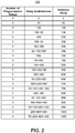
- FIG. 2 is a table 200 illustrating exemplary delays achieved using one or more of the programmable delays described with reference to FIG. 1 .
- the left column entitled “Number of Programmable Delays” indicates the number of programmable delays that must be used serially, e.g., cascaded or daisy chained, to achieve the total amount of delay in the right column entitled “Achieved Delay.”
- the middle column entitled “Delay Contributions” shows the amount of delay that is contributed by each of the serially connected, individual programmable delays.
- each programmable circuit may contribute as little as 50 picoseconds of delay and a maximum of 400 picoseconds of delay. As illustrated in Table 200, more than 1,050 picoseconds of delay may be achieved by cascading 4 programmable delays together. The amount of delay applied by one or more programmable delays using a cascaded architecture increases in increments of 50 picoseconds, which is the smallest amount of delay that may be applied by a single one of programmable delays 100.
- FIG. 3 is a circuit diagram illustrating an exemplary cascaded architecture 300 using programmable delays.
- FIG. 3 illustrates an example in which programmable delay A processes a first clock signal, while programmable delay B processes a second, independent clock signal.
- a clock signal is received at Clk In (clock input 114) of each of programmable delays A and B, is passed through the delay line of each programmable delay, and is then passed to Clk Out (clock output 152) of programmable delays A and B.
- Clk In clock input 114
- Clk Out clock output 152
- Csc Out cascaded output 148)
- Csc In cascaded input 112
- FIG. 4 is a circuit diagram illustrating another exemplary cascaded architecture 400 using programmable delays.
- FIG. 4 illustrates an example in which a programmable delay B is not used and, therefore, is available for further processing a clock signal initially processed using programmable delay A.
- a clock signal is received at Clk In of programmable delay A, is delayed through the delay line, and output at Csc Out of programmable delay A.
- the original clock signal received at Clk In of programmable delay A is output from Clk Out for use by one or more clock loads.
- Csc Out of programmable delay A is coupled to Csc In of programmable delay B.
- Cascaded architecture 400 illustrates an example where the amount of delay that may be generated for the signal output from Clk Out of programmable delay B may be twice that of an individual programmable delay.
- FIG. 5 is a circuit diagram illustrating another exemplary cascaded architecture 500 using programmable delays.
- cascaded architecture 500 a first clock signal received at Csc In of programmable delay A, processed through the delay line, and output from Csc Out of programmable delay A.
- Csc Out of programmable delay A is coupled to Csc In of programmable delay B and further delayed through the delay line of programmable delay B, before being output at Clk Out of programmable delay B.
- the first clock signal output through Clk Out of programmable delay B may have up to three times the total available delay provided by a single one of the programmable delays since the Csc In of programmable delay A is fed by a Csc Out of a previous programmable delay not shown.
- Programmable delay A further receives a second, independent clock signal at Clk In.
- the second clock signal is passed through programmable delay A without adding any additional delay and is output through Clk Out.
- FIG. 6 is a circuit diagram illustrating another exemplary cascaded architecture 600 using programmable delays.
- cascaded architecture 600 two separate and independent clock signals are processed to generate two separate and independent pulse signals.
- Each of programmable delays A and B receives a clock signal at Clk In.
- the clock signal is delayed in the delay line of each of programmable delays A and B and then used to create a pulse signal by performing a NAND operation on the delayed clock signal and the original clock signal without delay.
- the resulting pulse signal is output from Clk Out of each of programmable delays A and B.
- FIG. 7 is a circuit diagram illustrating another exemplary cascaded architecture 700 using programmable delays.
- programmable delays A and B are cascaded to achieve a delay of twice that of a single one of the programmable delays.
- the delayed signal is then used to create a pulse signal in programmable delay B having twice the pulse width of a pulse signal generated using a single one of the programmable delays.
- a clock signal is received at Clk In of programmable delay A.
- the clock signal is delayed using the delay line in programmable delay A and output from Csc Out.
- the delayed clock signal is received at Csc In of programmable delay B, further delayed using the delay line of programmable delay B, and provided to the pulse generator therein.
- the original clock signal received at Clk In of programmable delay A also is passed through to Clk Out of programmable delay A without any delay being added and is available for use by clock loads local to programmable delay A.
- the original clock signal also may be passed to Clk In of programmable delay B using additional wire resources external to programmable delay A and used for generation of the pulse signal by the pulse generator in programmable delay B.
- a second and independent clock signal may be provided to the Clk In of programmable delay B illustrated in dashed line. The resulting pulse signal is output from Clk Out of programmable delay B.
- FIG. 8 is a circuit diagram illustrating another exemplary cascaded architecture 800 using programmable delays.
- programmable delay A receives a clock signal at Clk In.
- the clock signal is delayed using the delay line of programmable delay A.
- the delayed clock signal is then provided to the pulse generator along with the original clock signal to generate a pulse signal using the pulse generator of programmable delay A.
- the pulse signal is output by both Csc Out and Clk Out of programmable delay A.
- the pulse signal from Clk Out may be used to drive clock loads in and around Clk Out of programmable delay A.
- the pulse signal from Csc Out is provided to Csc In of programmable delay B.
- the pulse signal is delayed using the delay line of programmable delay B and output through Clk Out of programmable delay B.
- FIG. 9 is a circuit diagram illustrating another exemplary cascaded architecture 900 using programmable delays.
- the example of cascaded architecture 900 is substantially similar to that of cascaded architecture 800.
- One exception is that programmable delay A does not output the pulse signal from both Csc Out and Clk Out. Rather, programmable delay A outputs the pulse signal from Csc Out, while outputting the original clock signal without any additional delay from Clk Out.
- the pulse signal output from Csc Out is provided to Csc In of programmable delay B, delayed through the delay line of programmable delay B, and output through Clk Out.
- FIG. 10 is a block diagram illustrating another exemplary cascaded architecture 1000 using programmable delays.
- Cascaded architecture 1000 includes 4 programmable delays A, B, C, and D cascaded together.
- cascade output 148 of programmable delay A is coupled to cascade input 112 of programmable delay B.
- Cascade output 148 of programmable delay B is coupled to cascade input 112 of programmable delay C.
- Cascade output 148 of programmable delay C is coupled to cascade input 112 of programmable delay D.
- cascade output 148 of programmable delay D is coupled to cascade input 112 of programmable delay A.
- Cascaded architecture 1000 allows a total delay of up to 4 times that of a single programmable delay to be applied to a received clock signal. Further, pulse signals having a pulse width of up to 4 times the pulse width of a pulse signal generated by a single programmable delay may be generated. In that case, programmable delay A is used as a signal entry point while the resulting output signal is output from clock output 152 of programmable delay D.
- an output signal may be taken from clock output 152 of any of programmable delays A, B, C, and/or D depending upon the amount of delay, the pulse width that is desired, and/or the location in the IC that the clock signal is needed.
- the signal entry point may vary and be a clock input 114 of any of programmable delays A, B, C, and/or D.
- a clock architecture may be created in which a signal enters programmable delay B through clock input 114, cascades through programmable delays C and D using cascade outputs 148, and is cascaded using the loop back connection to programmable delay A.
- the resulting signal may be output from clock output 152 of programmable delay A. While the examples described with reference to FIG. 10 utilize all four of the illustrated programmable delays, clock architectures of fewer than all of the illustrated delays may also be created. Within a given set of programmable delays arranged in a loop back configuration as shown within an IC, e.g., whether 2, 3, 4, or more programmable delays for the loop back configuration, the entry and exit points for the clock signal may be selected independently of one another.
- FIG. 11 is a block diagram illustrating another exemplary cascaded architecture 1100 using programmable delays.
- Cascaded architecture 1100 includes four programmable delays A, B, C, and D.
- programmable delays are cascaded together as two separate pairs.
- cascade output 148 of programmable delay A is coupled to cascade input 112 of programmable delay B.
- Cascade output 148 of programmable delay B is coupled to cascade input 112 of programmable delay A.
- cascade output 148 of programmable delay C is coupled to cascade input 112 of programmable delay D.
- Cascade output 148 of programmable delay D is coupled to cascade input 112 of programmable delay C.
- Each pair of cascaded programmable delays may provide up to 2 times the delay of a single programmable delay and a pulse signal having a pulse width of up to 2 times that of a single programmable delay.
- One resulting output signal is output from clock output 152 of programmable delay B.
- Another resulting output signal is output from clock output 152 of programmable delay D.
- connections between cascade output and a cascade input of the programmable delays may be fixed, i.e., created as a hardwired connection as part of the IC in which the programmable delays are implemented.
- a leaf of a clock architecture, or clock tree is a node where the clock signal leaves a routing track (wire) that delivers the clock signal from a clock source to a particular region or zone of the IC, at which point the clock signal switches to a distribution track (wire) for distribution to one or more clock loads local to the leaf node.
- selected ones of the programmable delays are coupled together to form one or more cascaded architectures as illustrated within this specification.
- Two, or more, programmable delays are coupled by connecting a cascade output of one programmable delay with a cascade input of another programmable delay.
- each programmable delay may be a hardwired, or fixed circuit block, that is configurable.
- the wiring between two, or more, cascaded programmable delays that connects a cascade output to a cascade input may be a hardwired, or fixed, connection within the IC.
- FIG. 13 is a block diagram illustrating an exemplary architecture 1300 for an IC.
- architecture 1300 is implemented within a field programmable gate array (FPGA) type of IC.
- Architecture 1300 is also representative of an SOC type of IC.
- an SOC is an IC that includes a processor that executes program code and one or more other circuits and/or circuit systems. The circuits and/or circuit systems may operate cooperatively with one another and with the processor.
- the programmable delays described within this disclosure may be implemented throughout the clock areas illustrated in FIG. 13 .
- architecture 1300 includes several different types of programmable circuit, e.g., logic, blocks.
- architecture 1300 may include a large number of different programmable tiles including multi-gigabit transceivers (MGTs) 1301, configurable logic blocks (CLBs) 1302, random access memory blocks (BRAMs) 1303, input/output blocks (lOBs) 1304, configuration and clocking logic (CONFIG/CLOCKS) 1305, digital signal processing blocks (DSPs) 1306, specialized I/O blocks 1307 (e.g., configuration ports and clock ports), and other programmable logic 1308 such as digital clock managers, analog-to-digital converters, system monitoring logic, and so forth.
- MTTs multi-gigabit transceivers
- CLBs configurable logic blocks
- BRAMs random access memory blocks
- lOBs input/output blocks
- CONFIG/CLOCKS configuration and clocking logic
- DSPs digital signal processing blocks
- I/O blocks 1307 e.g., configuration ports and clock ports
- a CLB 1302 can include a configurable logic element (CLE) 1312 that may be programmed to implement user logic plus a single INT 1311.
- a BRAM 1303 may include a BRAM logic element (BRL) 1313 in addition to one or more INTs 1311.
- BRAM logic element BRAM logic element
- the number of INTs 1311 included in a tile depends on the height of the tile. As pictured, a BRAM tile has the same height as five CLBs, but other numbers (e.g., four) may also be used.
- a DSP tile 1306 may include a DSP logic element (DSPL) 1314 in addition to an appropriate number of INTs 1311.
- DSPL DSP logic element
- An IOB 1304 may include, for example, two instances of an I/O logic element (IOL) 1315 in addition to one instance of an INT 1311.
- IOL I/O logic element
- a columnar area near the center of the die e.g., formed of regions 1305, 1307, and 1308, may be used for configuration, clock, and other control logic.
- Horizontal areas 1309 extending from this column are used to distribute the clocks and configuration signals across the breadth of the programmable IC.
- One or more programmable delays may be implemented on clock lines distributed throughout regions 1305, 1307, 1308, and/or 1309.
- clock circuits may be implemented in various locations within architecture 300.
- Such clock circuits may include a programmable delay as described within this disclosure.
- a clock circuit including a programmable delay may be included, or located, at the intersection of region 1309 with one or more or each of columns including CLBs 1302, BRAMs 1303, and/or DSPs 1306. It should be appreciated, however, that the programmable delays may be included or located elsewhere within architecture 300 and that the examples provided herein are not intended to be limiting.
- Some ICs utilizing the architecture illustrated in FIG. 13 include additional logic blocks that disrupt the regular columnar structure making up a large part of the IC.
- the additional logic blocks may be programmable blocks and/or dedicated circuitry.
- PROC 1310 spans several columns of CLBs and BRAMs.
- PROC 1310 is implemented as a dedicated circuitry, e.g., as a hard-wired processor, that is fabricated as part of the die that implements the programmable circuitry of the IC.
- PROC 1310 may represent any of a variety of different processor types and/or systems ranging in complexity from an individual processor, e.g., a single core capable of executing program code, to an entire processor system having one or more cores, modules, co-processors, interfaces, or the like.
- programmable circuitry means programmable circuit elements within an IC, e.g., the various programmable or configurable circuit blocks or tiles described herein, as well as the interconnect circuitry that selectively couples the various circuit blocks, tiles, and/or elements according to configuration data that is loaded into the IC.
- portions shown in FIG. 13 that are external to PROC 1310 such as CLBs 1302 and BRAMs 1303 are considered programmable circuitry of the IC.
- Programmable circuitry may be configured or programmed to implement different physical circuits therein.
- hardwired circuitry e.g., the programmable delays
- the operational modes may be set, for example, through the loading of a configuration bitstream into the IC.
- hardwired circuitry is not considered programmable circuitry as the hardwired circuitry is operable and has a particular function when manufactured as part of the IC.
- a programmable delay circuit block and cascade architectures formed of two or more programmable delays are described.
- the inventive arrangements when incorporated into a clock architecture of an IC, provide increased flexibility and control over clock signals and clock signal generation. Skew of clock signals may be controlled with increased accuracy. Further, pulse signals having a programmable pulse width may be generated thereby facilitating conversion of selected clocked circuit elements into latches to implement time borrowing operations when such selected, clocked elements are clocked using the pulse signal.
- the term “and/or” means any and all possible combinations of one or more of the associated listed items.
- first,” “second,” etc. may be used herein to describe various elements, these elements should not be limited by these terms, as these terms are only used to distinguish one element from another unless the context indicates otherwise.
- the same reference characters are used to refer to terminals, signal lines, wires, and their corresponding signals.
- the terms “signal,” “wire,” “connection,” “terminal,” and “pin” may be used interchangeably, from time-to-time, within this disclosure.
- the terms “signal,” “wire,” or the like may represent one or more signals, e.g., the conveyance of a single bit through a single wire or the conveyance of multiple parallel bits through multiple parallel wires.
- each wire or signal may represent bi-directional communication between two, or more, components connected by a signal or wire as the case may be.
- each block in the flowchart or block diagrams may represent a module, segment, or portion of code, which includes one or more executable instructions for implementing the specified function(s).
- each block of the block diagrams and/or flowchart illustration, and combinations of blocks in the block diagrams and/or flowchart illustration can be implemented by special purpose hardware-based systems that perform the specified functions or acts, or combinations of special purpose hardware and computer instructions.
- a programmable delay circuit block includes an input stage having a cascade input and a clock input, wherein the input stage passes a signal received at the cascade input or a signal received at the clock input, a delay block configured to generate a delayed signal by applying a selected amount of delay to the signal passed from the input stage, and a pulse generator configured to generate a pulse signal having a pulse width that depends upon the amount of delay.
- the programmable delay circuit block also includes an output stage having a cascade output and a clock output. The output stage is configured to pass an inverted version of the pulse signal or the delayed signal from the cascade output and pass the signal received at the clock input, the inverted version of the pulse signal, or the delayed signal from the clock output.
- the input stage includes a memory cell and passes either the signal at the cascade input or the signal received at the clock input according to a value stored in the memory cell. Further, the input stage may selectively gate the signal received at the clock input according to a value stored in a memory cell.
- the delay block may include a delay line having multiple taps and generating a plurality of candidate delayed signals.
- the delay block may also include a delay selector block passing one of the plurality of candidate delayed signals as the delayed signal.
- the delay line may be binary weighted.
- a clock circuit includes a first programmable delay circuit block having a first cascade input, a first clock input, a first delay line having multiple taps, a first pulse generator, a first cascade output, and a first clock output.
- the clock circuit also includes a second programmable delay circuit block having a second cascade input, a second clock input, a second delay line having multiple taps, a second pulse generator, a second cascade output, and a second clock output.
- the first cascade output is coupled to the second cascade input.
- the first cascade output may pass an inverted version of a first pulse signal generated by the first pulse generator or a first delayed signal generated by the first delay line.
- the second cascade output may pass an inverted version of a second pulse signal generated by the second pulse generator or a second delayed signal generated by the second delay line.
- the first clock output may pass a signal received at the first clock input, the inverted version of the first pulse signal, or the first delayed signal.
- the second clock output may pass a second signal received at the second clock input, the inverted version of the second pulse signal, or the second delayed signal.
- the first pulse generator generates a first pulse signal having a pulse width that depends upon an amount of delay applied to a signal by the first delay line.
- the second pulse generator generates a second pulse signal having a pulse width that depends upon an amount of delay applied to a signal by the second delay line.
- the first programmable delay may delay a first clock signal and output the delayed first clock signal through the first cascade output.
- the second programmable delay may receive the delayed first clock signal through the second cascade input and further delay the delayed first clock signal.
- the first programmable delay may output the first clock signal from the first clock output without applying a delay.
- the first clock signal may be received in the first programmable delay at the first cascade input. In that case, the first programmable delay may receive a second clock signal independent of the first clock signal at the first clock input and output the second clock signal from the first clock output without applying a delay.
- the first programmable delay may delay a first clock signal and output the delayed first clock signal through the first cascade output.
- the second programmable delay may receive the delayed first clock signal at the second cascade input, further delay the delayed first clock signal, generate a pulse signal using the further delayed first clock signal, and output an inverted version of the pulse signal.
- the first programmable delay may further output the first clock signal through the first clock output without a delay.
- the second programmable delay may receive a second clock signal independent of the first clock signal at the second clock input and use the second clock signal and the further delayed first clock signal within the pulse generator to generate the pulse signal.
- the first programmable delay may generate a pulse signal from a received clock signal and output an inverted version of the pulse signal through the first cascade output.
- the second programmable delay may receive the inverted version of the pulse signal at the second cascade input, delay the inverted version of the pulse signal, and output the delayed inverted version of the pulse signal. In that case, the first programmable delay may further output the inverted version of the pulse signal from the first clock output.
- the first cascade output may be coupled to the second cascade input using fixed circuitry.
Landscapes
- Physics & Mathematics (AREA)
- Nonlinear Science (AREA)
- Mathematical Physics (AREA)
- Engineering & Computer Science (AREA)
- Computer Hardware Design (AREA)
- Computing Systems (AREA)
- General Engineering & Computer Science (AREA)
- Pulse Circuits (AREA)
- Manipulation Of Pulses (AREA)
Claims (13)
- Programmierbarer Verzögerungsschaltungsblock (100), umfassend:eine Eingangsstufe (102), umfassend einen Kaskadeneingang (112) und einen Takteingang (114);wobei die Eingangsstufe (102) eine Speicherzelle (MC[4]) umfasst und entweder das Signal an dem Kaskadeneingang (112) oder das an dem Takteingang (114) empfangene Signal gemäß einem in der Speicherzelle (MC[4]) gespeicherten Wert weiterleitet;einen Verzögerungsblock (104), der mit einem Ausgang der Eingangsstufe gekoppelt ist und dazu konfiguriert ist, ein verzögertes Signal durch Anwenden eines ausgewählten Verzögerungsbetrags auf das von der Eingangsstufe (102) weitergeleitete Signal zu erzeugen;einen Impulsgenerator (134), der mit einem Ausgang des Verzögerungsblocks gekoppelt ist und dazu konfiguriert ist, ein Impulssignal (138) zu erzeugen, das eine Impulsbreite aufweist, die von dem durch den Verzögerungsblock (104) angewendeten Verzögerungsbetrag abhängt; undeine Ausgangsstufe (108), die mit einem Ausgang des Impulsgenerators (134) gekoppelt ist, wobei die Ausgangsstufe (108) einen Kaskadenausgang (148) und einen Taktausgang (152) für den programmierbaren Verzögerungsschaltungsblock (100) umfasst;wobei die Ausgangsstufe (108) konfigurierbar ist, um eine invertierte Version des Impulssignals oder das verzögerte Signal an den Kaskadenausgang (148) weiterzuleiten, und konfigurierbar ist, um das an dem Takteingang empfangene Signal, die invertierte Version des Impulssignals oder das verzögerte Signal an den Taktausgang (152) weiterzuleiten.
- Programmierbarer Verzögerungsschaltungsblock (100) nach Anspruch 1, wobei die Eingangsstufe (102) das an dem Takteingang (114) empfangene Signal selektiv gemäß einem in einer Speicherzelle (MC[2]), (MC[3]) und/oder (MC[4]) gespeicherten Wert gattert.
- Programmierbarer Verzögerungsschaltungsblock (100) nach einem der Ansprüche 1 und 2, wobei der Impulsgenerator (106) eine NAND-Schaltung (136) umfasst, die das Impulssignal aus einer invertierten Version des verzögerten Signals und dem an dem Takteingang (114) empfangenen Signal erzeugt.
- Programmierbarer Verzögerungsschaltungsblock (100) nach einem der Ansprüche 1 bis 3, wobei der Verzögerungsblock (104) umfasst:eine Verzögerungsleitung (124), die mehrere Abgriffe aufweist und eine Vielzahl von in Frage kommenden verzögerten Signalen erzeugt; undeinen Verzögerungsauswahlblock (126), der eines aus der Vielzahl von in Frage kommenden verzögerten Signalen als das verzögerte Signal weiterleitet.
- Programmierbarer Verzögerungsschaltungsblock (100) nach Anspruch 4, wobei:der Verzögerungsauswahlblock (126) eine Speicherzelle (MC[1]) und einen invertierenden Multiplexer (132) umfasst; undder invertierende Multiplexer (132) das verzögerte Signal aus der Vielzahl von in Frage kommenden verzögerten Signalen gemäß einem in der Speicherzelle (MC[1]) gespeicherten Wert auswählt.
- Programmierbarer Verzögerungsschaltungsblock (100) nach einem der Ansprüche 1 bis 5, wobei:die Ausgangsstufe (108) ferner eine Vielzahl von Speicherzellen (MC[2]), (MC[3]), einen Multiplexer (142) und einen invertierenden Multiplexer (148) umfasst;der Multiplexer (142) das Impulssignal oder eine invertierte Version des verzögerten Signals an den Kaskadenausgang (148) gemäß einem in einer ersten aus der Vielzahl von Speicherzellen (MC[2]) gespeicherten Wert weitergibt; undder invertierende Multiplexer (148) eine invertierte Version des an dem Takteingang (114) empfangenen Signals, das Impulssignal oder die invertierte Version des verzögerten Signals an den Taktausgang (152) gemäß dem in der ersten Speicherzelle (MC[2]) gespeicherten Wert und einem in einer zweiten aus der Vielzahl von Speicherzellen (MC[3]) gespeicherten Wert weitergibt.
- Taktschaltung, umfassend:einen ersten programmierbaren Verzögerungsschaltungsblock, umfassend eine erste Eingangsstufe (102), die einen ersten Kaskadeneingang (112), einen ersten Takteingang (114) und eine Speicherzelle (MC[4]) umfasst und dazu konfiguriert ist, entweder ein Signal an dem ersten Kaskadeneingang (112) oder ein Signal an dem ersten Takteingang (114) gemäß einem in der Speicherzelle (MC[4]) gespeicherten Wert weiterzuleiten, einen ersten Verzögerungsblock (104), der mit einem Ausgang der ersten Eingangsstufe (102) gekoppelt ist, wobei der erste Verzögerungsblock (104) einen ausgewählten Verzögerungsbetrag auf das von der ersten Eingangsstufe (102) weitergeleitete Signal anwendet, einen ersten Impulsgenerator (134), der mit einem Ausgang des ersten Verzögerungsblocks (104) gekoppelt ist, der dazu konfiguriert ist, ein erstes Impulssignal zu erzeugen, das eine Impulsbreite aufweist, die von dem durch den ersten Verzögerungsblock (104) angewendeten Verzögerungsbetrag abhängt, und eine erste Ausgangsstufe (108), die mit einem Ausgang des ersten Impulsgenerators (134) gekoppelt ist, wobei die erste Ausgangsstufe (108) einen ersten Kaskadenausgang (148) umfasst, der konfigurierbar ist, um ein erstes Ausgangssignal von dem ersten programmierbaren Verzögerungsschaltungsblock auszugeben, wobei das erste Ausgangssignal eine invertierte Version des ersten Impulssignals oder das erste Verzögerungssignal ist, und einen ersten Taktausgang (152), der konfigurierbar ist, um ein zweites Ausgangssignal von dem ersten programmierbaren Verzögerungsschaltungsblock auszugeben, wobei das zweite Ausgangssignal ein an dem ersten Takteingang (114) empfangenes Signal, das invertierte Signal des ersten Impulssignals oder das erste verzögerte Signal ist; undeinen zweiten programmierbaren Verzögerungsschaltungsblock, umfassend eine zweite Eingangsstufe (102), die einen zweiten Kaskadeneingang (112), einen zweiten Takteingang (114) und eine Speicherzelle (MC[4]) umfasst und dazu konfiguriert ist, entweder ein Signal an dem zweiten Kaskadeneingang (112) oder ein Signal an dem zweiten Takteingang (114) gemäß einem in der Speicherzelle (MC[4]) gespeicherten Wert weiterzuleiten, einen zweiten Verzögerungsblock (104), der mit einem Ausgang der zweiten Eingangsstufe (102) gekoppelt ist, wobei der erste Verzögerungsblock (104) einen ausgewählten Verzögerungsbetrag auf das von der zweiten Eingangsstufe (102) weitergeleitete Signal anwendet, einen zweiten Impulsgenerator (134), der mit einem Ausgang des zweiten Verzögerungsblocks (104) gekoppelt ist, der dazu konfiguriert ist, ein zweites Impulssignal zu erzeugen, das eine Impulsbreite aufweist, die von dem durch den zweiten Verzögerungsblock (104) angewendeten Verzögerungsbetrag abhängt, und eine Ausgangsstufe (108), die mit einem Ausgang des zweiten Impulsgenerators (134) gekoppelt ist, wobei die zweite Ausgangsstufe (108) einen zweiten Kaskadenausgang (148) umfasst, der konfigurierbar ist, um ein erstes Ausgangssignal von dem zweiten programmierbaren Verzögerungsschaltungsblock auszugeben, wobei das erste Ausgangssignal eine invertierte Version des zweiten Impulssignals oder das zweite Verzögerungssignal ist, und einen zweiten Taktausgang (152), der konfigurierbar ist, um ein zweites Ausgangssignal von dem zweiten programmierbaren Verzögerungsschaltungsblock auszugeben, wobei das zweite Ausgangssignal ein an dem zweiten Takteingang (114) empfangenes Signal, das invertierte Signal des zweiten Impulssignals oder das zweite verzögerte Signal ist; undwobei der erste Kaskadenausgang (148) des ersten programmierbaren Verzögerungsschaltungsblocks mit dem zweiten Kaskadeneingang (112) des zweiten programmierbaren Verzögerungsschaltungsblocks gekoppelt ist.
- Taktschaltung nach Anspruch 7, wobei:der erste Kaskadenausgang (148) eine invertierte Version eines von dem ersten Impulsgenerator (134) erzeugten ersten Impulssignals oder ein von einer ersten Verzögerungsleitung (124) des ersten Verzögerungsblocks (104) erzeugtes erstes verzögertes Signal weiterleitet;der zweite Kaskadenausgang (148) eine invertierte Version eines von dem zweiten Impulsgenerator (134) erzeugten zweiten Impulssignals oder ein von einer zweiten Verzögerungsleitung (124) des zweiten Verzögerungsblocks (104) erzeugtes zweites verzögertes Signal weiterleitet;der erste Taktausgang (152) ein an dem ersten Takteingang (114) empfangenes Signal, die invertierte Version des ersten Impulssignals oder das erste verzögerte Signal weiterleitet; undder zweite Taktausgang (152) ein an dem zweiten Takteingang (114) empfangenes zweites Signal, die invertierte Version des zweiten Impulssignals oder das zweite verzögerte Signal weiterleitet.
- Taktschaltung nach Anspruch 7, wobei:der erste programmierbare Verzögerungsschaltungsblock ein erstes Taktsignal verzögert und das verzögerte erste Taktsignal über den ersten Kaskadenausgang (148) ausgibt; undder zweite programmierbare Verzögerungsschaltungsblock das verzögerte erste Taktsignal über den zweiten Kaskadeneingang (112) empfängt und das verzögerte erste Taktsignal weiter verzögert.
- Taktschaltung nach Anspruch 7, wobei:das erste Taktsignal in dem ersten programmierbaren Verzögerungsschaltungsblock an dem ersten Kaskadeneingang (112) empfangen wird;der erste programmierbare Verzögerungsschaltungsblock ein von dem ersten Taktsignal unabhängiges zweites Taktsignal an dem ersten Takteingang (114) empfängt und das zweite Taktsignal von dem ersten Taktausgang (152) ohne Anwenden einer Verzögerung ausgibt.
- Taktschaltung nach Anspruch 7, wobei:der erste programmierbare Verzögerungsschaltungsblock ein erstes Taktsignal verzögert und das verzögerte erste Taktsignal über den ersten Kaskadenausgang (148) ausgibt; undder zweite programmierbare Verzögerungsschaltungsblock das verzögerte erste Taktsignal an dem zweiten Kaskadeneingang (112) empfängt, das verzögerte erste Taktsignal weiter verzögert, ein Impulssignal unter Verwendung des weiter verzögerten ersten Taktsignals erzeugt und eine invertierte Version des Impulssignals ausgibt.
- Taktschaltung nach Anspruch 11,
wobei der zweite programmierbare Verzögerungsschaltungsblock ein von dem ersten Taktsignal unabhängiges zweites Taktsignal an dem zweiten Takteingang (114) empfängt und das zweite Taktsignal und das weiter verzögerte erste Taktsignal innerhalb des Impulsgenerators (134) verwendet, um das Impulssignal zu erzeugen. - Taktschaltung nach Anspruch 7, wobei:der erste programmierbare Verzögerungsschaltungsblock ein erstes Impulssignal aus einem empfangenen Taktsignal erzeugt und eine invertierte Version des ersten Impulssignals über den ersten Kaskadenausgang (148) ausgibt; undder zweite programmierbare Verzögerungsschaltungsblock die invertierte Version des ersten Impulssignals an dem zweiten Kaskadeneingang (112) empfängt, die invertierte Version des Impulssignals verzögert und die verzögerte invertierte Version des ersten Impulssignals ausgibt.
Applications Claiming Priority (2)
| Application Number | Priority Date | Filing Date | Title |
|---|---|---|---|
| US14/482,832 US9118310B1 (en) | 2014-09-10 | 2014-09-10 | Programmable delay circuit block |
| PCT/US2015/023790 WO2016039814A1 (en) | 2014-09-10 | 2015-04-01 | Programmable delay circuit block |
Publications (2)
| Publication Number | Publication Date |
|---|---|
| EP3192171A1 EP3192171A1 (de) | 2017-07-19 |
| EP3192171B1 true EP3192171B1 (de) | 2020-03-11 |
Family
ID=52875315
Family Applications (1)
| Application Number | Title | Priority Date | Filing Date |
|---|---|---|---|
| EP15716673.7A Active EP3192171B1 (de) | 2014-09-10 | 2015-04-01 | Programmierbarer verzögerungsschaltungsblock |
Country Status (6)
| Country | Link |
|---|---|
| US (1) | US9118310B1 (de) |
| EP (1) | EP3192171B1 (de) |
| JP (1) | JP6602849B2 (de) |
| KR (1) | KR102263674B1 (de) |
| CN (1) | CN106688182B (de) |
| WO (1) | WO2016039814A1 (de) |
Families Citing this family (6)
| Publication number | Priority date | Publication date | Assignee | Title |
|---|---|---|---|---|
| US9537491B1 (en) | 2015-03-24 | 2017-01-03 | Xilinx, Inc. | Leaf-level generation of phase-shifted clocks using programmable clock delays |
| US10284185B1 (en) * | 2017-12-18 | 2019-05-07 | Xilinx, Inc. | Selectively providing clock signals using a programmable control circuit |
| US11757439B2 (en) * | 2021-02-02 | 2023-09-12 | Efinix, Inc. | Chained programmable delay elements |
| US11803668B2 (en) * | 2021-07-30 | 2023-10-31 | Nvidia Corporation | Isolating a region of a system on a chip for safety critical operations |
| CN115913221B (zh) * | 2022-10-14 | 2025-08-08 | 中国电子科技集团公司第五十八研究所 | 一种应用于反熔丝型fpga内嵌pll_ip的可编程延迟电路 |
| JP2024071226A (ja) * | 2022-11-14 | 2024-05-24 | キヤノン株式会社 | プログラマブル信号処理装置、並びに、情報処理装置 |
Family Cites Families (17)
| Publication number | Priority date | Publication date | Assignee | Title |
|---|---|---|---|---|
| JPS63215212A (ja) * | 1987-03-04 | 1988-09-07 | Nec Corp | パルス回路 |
| JPH06310999A (ja) * | 1993-04-21 | 1994-11-04 | Olympus Optical Co Ltd | 2相パルス発生回路 |
| DE69407588T2 (de) * | 1994-09-21 | 1998-07-09 | Sgs Thomson Microelectronics | Programmierbare digitale Verzögerungsschaltungseinheit |
| DE19713130C2 (de) * | 1997-03-27 | 1999-01-14 | Endress Hauser Gmbh Co | Schaltungsanordnung zum Erzeugen zweier zeitlich gegeneinander verschobener Signale aus einem Taktsignal und zum Erzeugen eines von der zeitlichen Verschiebung abhängigen Meßsignals |
| JP3319340B2 (ja) * | 1997-05-30 | 2002-08-26 | 日本電気株式会社 | 半導体回路装置 |
| US5923197A (en) * | 1997-07-31 | 1999-07-13 | Credence Systems Corporation | Pulse stuffing circuit for programmable delay line |
| US6043677A (en) * | 1997-10-15 | 2000-03-28 | Lucent Technologies Inc. | Programmable clock manager for a programmable logic device that can implement delay-locked loop functions |
| KR100266679B1 (ko) * | 1998-04-16 | 2000-09-15 | 김영환 | 디램용 펄스발생회로 |
| US6246704B1 (en) * | 1998-04-30 | 2001-06-12 | Stmicroelectronics, Inc. | Automatic on-chip clock tuning methodology and circuitry |
| AU2216601A (en) * | 1999-12-28 | 2001-07-09 | Mellanox Technologies Ltd. | Variable delay generator |
| JP4986318B2 (ja) * | 2000-08-28 | 2012-07-25 | ルネサスエレクトロニクス株式会社 | 半導体装置 |
| US7250800B2 (en) * | 2005-07-12 | 2007-07-31 | Hewlett-Packard Development Company, L.P. | Clock pulse width control circuit |
| CN201113942Y (zh) * | 2007-08-03 | 2008-09-10 | 核工业理化工程研究院 | 脉冲延迟信号发生器 |
| CN102771049A (zh) * | 2010-03-26 | 2012-11-07 | 古河电气工业株式会社 | 延迟控制装置 |
| US8949652B2 (en) | 2011-11-03 | 2015-02-03 | Nvidia Corporation | Glitchless programmable clock shaper |
| US9093989B2 (en) * | 2011-11-21 | 2015-07-28 | Freescale Semiconductor, Inc. | Clock signal generator module, integrated circuit, electronic device and method therefor |
| CN102684651B (zh) * | 2012-05-25 | 2015-07-08 | 华为技术有限公司 | 用于数字电路的信号延迟方法、装置及数字电路系统 |
-
2014
- 2014-09-10 US US14/482,832 patent/US9118310B1/en active Active
-
2015
- 2015-04-01 CN CN201580048957.6A patent/CN106688182B/zh active Active
- 2015-04-01 JP JP2017513104A patent/JP6602849B2/ja active Active
- 2015-04-01 WO PCT/US2015/023790 patent/WO2016039814A1/en not_active Ceased
- 2015-04-01 EP EP15716673.7A patent/EP3192171B1/de active Active
- 2015-04-01 KR KR1020177009183A patent/KR102263674B1/ko not_active Expired - Fee Related
Non-Patent Citations (1)
| Title |
|---|
| None * |
Also Published As
| Publication number | Publication date |
|---|---|
| JP6602849B2 (ja) | 2019-11-06 |
| US9118310B1 (en) | 2015-08-25 |
| JP2017532850A (ja) | 2017-11-02 |
| KR20170051490A (ko) | 2017-05-11 |
| WO2016039814A1 (en) | 2016-03-17 |
| EP3192171A1 (de) | 2017-07-19 |
| CN106688182A (zh) | 2017-05-17 |
| KR102263674B1 (ko) | 2021-06-09 |
| CN106688182B (zh) | 2020-09-08 |
Similar Documents
| Publication | Publication Date | Title |
|---|---|---|
| EP3192171B1 (de) | Programmierbarer verzögerungsschaltungsblock | |
| US7868655B2 (en) | Configurable time borrowing flip-flops | |
| CN111512552B (zh) | 使用可编程控制电路选择性地提供时钟信号 | |
| US8115530B2 (en) | Robust time borrowing pulse latches | |
| US7116131B1 (en) | High performance programmable logic devices utilizing dynamic circuitry | |
| US9685957B2 (en) | System reset controller replacing individual asynchronous resets | |
| CN109905116B (zh) | 可编程流水线接口电路 | |
| US8988125B1 (en) | Circuits for and methods of routing signals in an integrated circuit | |
| US9007110B1 (en) | Register circuits and methods of storing data in a register circuit | |
| US9355690B1 (en) | Time-multiplexed, asynchronous device | |
| US9018980B1 (en) | Bimodal clock generator | |
| US10069486B1 (en) | Multimode registers with pulse latches | |
| US9235498B1 (en) | Circuits for and methods of enabling the modification of an input data stream | |
| US7382170B2 (en) | Programmable delay circuit having reduced insertion delay | |
| US10979034B1 (en) | Method and apparatus for multi-voltage domain sequential elements | |
| US9729153B1 (en) | Multimode multiplexer-based circuit | |
| US9372953B1 (en) | Increasing operating frequency of circuit designs using dynamically modified timing constraints | |
| US20150162918A1 (en) | Digital output clock generation | |
| US10534729B1 (en) | Method and apparatus for inter-die data transfer | |
| US11757439B2 (en) | Chained programmable delay elements | |
| US7683666B1 (en) | Circuit component with programmable characteristics and method of operating same |
Legal Events
| Date | Code | Title | Description |
|---|---|---|---|
| STAA | Information on the status of an ep patent application or granted ep patent |
Free format text: STATUS: THE INTERNATIONAL PUBLICATION HAS BEEN MADE |
|
| PUAI | Public reference made under article 153(3) epc to a published international application that has entered the european phase |
Free format text: ORIGINAL CODE: 0009012 |
|
| STAA | Information on the status of an ep patent application or granted ep patent |
Free format text: STATUS: REQUEST FOR EXAMINATION WAS MADE |
|
| 17P | Request for examination filed |
Effective date: 20170410 |
|
| AK | Designated contracting states |
Kind code of ref document: A1 Designated state(s): AL AT BE BG CH CY CZ DE DK EE ES FI FR GB GR HR HU IE IS IT LI LT LU LV MC MK MT NL NO PL PT RO RS SE SI SK SM TR |
|
| AX | Request for extension of the european patent |
Extension state: BA ME |
|
| DAV | Request for validation of the european patent (deleted) | ||
| DAX | Request for extension of the european patent (deleted) | ||
| RIC1 | Information provided on ipc code assigned before grant |
Ipc: H03K 5/135 20060101ALI20190401BHEP Ipc: H03K 5/15 20060101AFI20190401BHEP Ipc: H03K 19/173 20060101ALI20190401BHEP Ipc: H03K 19/177 20060101ALI20190401BHEP Ipc: H03K 5/14 20140101ALI20190401BHEP Ipc: H03K 5/156 20060101ALI20190401BHEP |
|
| GRAP | Despatch of communication of intention to grant a patent |
Free format text: ORIGINAL CODE: EPIDOSNIGR1 |
|
| STAA | Information on the status of an ep patent application or granted ep patent |
Free format text: STATUS: GRANT OF PATENT IS INTENDED |
|
| INTG | Intention to grant announced |
Effective date: 20190513 |
|
| GRAJ | Information related to disapproval of communication of intention to grant by the applicant or resumption of examination proceedings by the epo deleted |
Free format text: ORIGINAL CODE: EPIDOSDIGR1 |
|
| STAA | Information on the status of an ep patent application or granted ep patent |
Free format text: STATUS: REQUEST FOR EXAMINATION WAS MADE |
|
| INTC | Intention to grant announced (deleted) | ||
| GRAP | Despatch of communication of intention to grant a patent |
Free format text: ORIGINAL CODE: EPIDOSNIGR1 |
|
| STAA | Information on the status of an ep patent application or granted ep patent |
Free format text: STATUS: GRANT OF PATENT IS INTENDED |
|
| INTG | Intention to grant announced |
Effective date: 20191004 |
|
| GRAS | Grant fee paid |
Free format text: ORIGINAL CODE: EPIDOSNIGR3 |
|
| GRAA | (expected) grant |
Free format text: ORIGINAL CODE: 0009210 |
|
| STAA | Information on the status of an ep patent application or granted ep patent |
Free format text: STATUS: THE PATENT HAS BEEN GRANTED |
|
| AK | Designated contracting states |
Kind code of ref document: B1 Designated state(s): AL AT BE BG CH CY CZ DE DK EE ES FI FR GB GR HR HU IE IS IT LI LT LU LV MC MK MT NL NO PL PT RO RS SE SI SK SM TR |
|
| REG | Reference to a national code |
Ref country code: GB Ref legal event code: FG4D |
|
| REG | Reference to a national code |
Ref country code: CH Ref legal event code: EP |
|
| REG | Reference to a national code |
Ref country code: AT Ref legal event code: REF Ref document number: 1244426 Country of ref document: AT Kind code of ref document: T Effective date: 20200315 |
|
| REG | Reference to a national code |
Ref country code: IE Ref legal event code: FG4D |
|
| REG | Reference to a national code |
Ref country code: DE Ref legal event code: R096 Ref document number: 602015048544 Country of ref document: DE |
|
| PG25 | Lapsed in a contracting state [announced via postgrant information from national office to epo] |
Ref country code: RS Free format text: LAPSE BECAUSE OF FAILURE TO SUBMIT A TRANSLATION OF THE DESCRIPTION OR TO PAY THE FEE WITHIN THE PRESCRIBED TIME-LIMIT Effective date: 20200311 Ref country code: NO Free format text: LAPSE BECAUSE OF FAILURE TO SUBMIT A TRANSLATION OF THE DESCRIPTION OR TO PAY THE FEE WITHIN THE PRESCRIBED TIME-LIMIT Effective date: 20200611 Ref country code: FI Free format text: LAPSE BECAUSE OF FAILURE TO SUBMIT A TRANSLATION OF THE DESCRIPTION OR TO PAY THE FEE WITHIN THE PRESCRIBED TIME-LIMIT Effective date: 20200311 |
|
| REG | Reference to a national code |
Ref country code: NL Ref legal event code: MP Effective date: 20200311 |
|
| PG25 | Lapsed in a contracting state [announced via postgrant information from national office to epo] |
Ref country code: LV Free format text: LAPSE BECAUSE OF FAILURE TO SUBMIT A TRANSLATION OF THE DESCRIPTION OR TO PAY THE FEE WITHIN THE PRESCRIBED TIME-LIMIT Effective date: 20200311 Ref country code: SE Free format text: LAPSE BECAUSE OF FAILURE TO SUBMIT A TRANSLATION OF THE DESCRIPTION OR TO PAY THE FEE WITHIN THE PRESCRIBED TIME-LIMIT Effective date: 20200311 Ref country code: BG Free format text: LAPSE BECAUSE OF FAILURE TO SUBMIT A TRANSLATION OF THE DESCRIPTION OR TO PAY THE FEE WITHIN THE PRESCRIBED TIME-LIMIT Effective date: 20200611 Ref country code: HR Free format text: LAPSE BECAUSE OF FAILURE TO SUBMIT A TRANSLATION OF THE DESCRIPTION OR TO PAY THE FEE WITHIN THE PRESCRIBED TIME-LIMIT Effective date: 20200311 Ref country code: GR Free format text: LAPSE BECAUSE OF FAILURE TO SUBMIT A TRANSLATION OF THE DESCRIPTION OR TO PAY THE FEE WITHIN THE PRESCRIBED TIME-LIMIT Effective date: 20200612 |
|
| REG | Reference to a national code |
Ref country code: LT Ref legal event code: MG4D |
|
| PG25 | Lapsed in a contracting state [announced via postgrant information from national office to epo] |
Ref country code: NL Free format text: LAPSE BECAUSE OF FAILURE TO SUBMIT A TRANSLATION OF THE DESCRIPTION OR TO PAY THE FEE WITHIN THE PRESCRIBED TIME-LIMIT Effective date: 20200311 |
|
| PG25 | Lapsed in a contracting state [announced via postgrant information from national office to epo] |
Ref country code: SK Free format text: LAPSE BECAUSE OF FAILURE TO SUBMIT A TRANSLATION OF THE DESCRIPTION OR TO PAY THE FEE WITHIN THE PRESCRIBED TIME-LIMIT Effective date: 20200311 Ref country code: CZ Free format text: LAPSE BECAUSE OF FAILURE TO SUBMIT A TRANSLATION OF THE DESCRIPTION OR TO PAY THE FEE WITHIN THE PRESCRIBED TIME-LIMIT Effective date: 20200311 Ref country code: RO Free format text: LAPSE BECAUSE OF FAILURE TO SUBMIT A TRANSLATION OF THE DESCRIPTION OR TO PAY THE FEE WITHIN THE PRESCRIBED TIME-LIMIT Effective date: 20200311 Ref country code: IS Free format text: LAPSE BECAUSE OF FAILURE TO SUBMIT A TRANSLATION OF THE DESCRIPTION OR TO PAY THE FEE WITHIN THE PRESCRIBED TIME-LIMIT Effective date: 20200711 Ref country code: EE Free format text: LAPSE BECAUSE OF FAILURE TO SUBMIT A TRANSLATION OF THE DESCRIPTION OR TO PAY THE FEE WITHIN THE PRESCRIBED TIME-LIMIT Effective date: 20200311 Ref country code: SM Free format text: LAPSE BECAUSE OF FAILURE TO SUBMIT A TRANSLATION OF THE DESCRIPTION OR TO PAY THE FEE WITHIN THE PRESCRIBED TIME-LIMIT Effective date: 20200311 Ref country code: PT Free format text: LAPSE BECAUSE OF FAILURE TO SUBMIT A TRANSLATION OF THE DESCRIPTION OR TO PAY THE FEE WITHIN THE PRESCRIBED TIME-LIMIT Effective date: 20200805 Ref country code: LT Free format text: LAPSE BECAUSE OF FAILURE TO SUBMIT A TRANSLATION OF THE DESCRIPTION OR TO PAY THE FEE WITHIN THE PRESCRIBED TIME-LIMIT Effective date: 20200311 |
|
| REG | Reference to a national code |
Ref country code: AT Ref legal event code: MK05 Ref document number: 1244426 Country of ref document: AT Kind code of ref document: T Effective date: 20200311 |
|
| REG | Reference to a national code |
Ref country code: CH Ref legal event code: PL |
|
| REG | Reference to a national code |
Ref country code: DE Ref legal event code: R097 Ref document number: 602015048544 Country of ref document: DE |
|
| PG25 | Lapsed in a contracting state [announced via postgrant information from national office to epo] |
Ref country code: MC Free format text: LAPSE BECAUSE OF FAILURE TO SUBMIT A TRANSLATION OF THE DESCRIPTION OR TO PAY THE FEE WITHIN THE PRESCRIBED TIME-LIMIT Effective date: 20200311 |
|
| PLBE | No opposition filed within time limit |
Free format text: ORIGINAL CODE: 0009261 |
|
| STAA | Information on the status of an ep patent application or granted ep patent |
Free format text: STATUS: NO OPPOSITION FILED WITHIN TIME LIMIT |
|
| PG25 | Lapsed in a contracting state [announced via postgrant information from national office to epo] |
Ref country code: ES Free format text: LAPSE BECAUSE OF FAILURE TO SUBMIT A TRANSLATION OF THE DESCRIPTION OR TO PAY THE FEE WITHIN THE PRESCRIBED TIME-LIMIT Effective date: 20200311 Ref country code: CH Free format text: LAPSE BECAUSE OF NON-PAYMENT OF DUE FEES Effective date: 20200430 Ref country code: DK Free format text: LAPSE BECAUSE OF FAILURE TO SUBMIT A TRANSLATION OF THE DESCRIPTION OR TO PAY THE FEE WITHIN THE PRESCRIBED TIME-LIMIT Effective date: 20200311 Ref country code: AT Free format text: LAPSE BECAUSE OF FAILURE TO SUBMIT A TRANSLATION OF THE DESCRIPTION OR TO PAY THE FEE WITHIN THE PRESCRIBED TIME-LIMIT Effective date: 20200311 Ref country code: IT Free format text: LAPSE BECAUSE OF FAILURE TO SUBMIT A TRANSLATION OF THE DESCRIPTION OR TO PAY THE FEE WITHIN THE PRESCRIBED TIME-LIMIT Effective date: 20200311 Ref country code: LU Free format text: LAPSE BECAUSE OF NON-PAYMENT OF DUE FEES Effective date: 20200401 Ref country code: LI Free format text: LAPSE BECAUSE OF NON-PAYMENT OF DUE FEES Effective date: 20200430 |
|
| REG | Reference to a national code |
Ref country code: BE Ref legal event code: MM Effective date: 20200430 |
|
| 26N | No opposition filed |
Effective date: 20201214 |
|
| PG25 | Lapsed in a contracting state [announced via postgrant information from national office to epo] |
Ref country code: SI Free format text: LAPSE BECAUSE OF FAILURE TO SUBMIT A TRANSLATION OF THE DESCRIPTION OR TO PAY THE FEE WITHIN THE PRESCRIBED TIME-LIMIT Effective date: 20200311 Ref country code: PL Free format text: LAPSE BECAUSE OF FAILURE TO SUBMIT A TRANSLATION OF THE DESCRIPTION OR TO PAY THE FEE WITHIN THE PRESCRIBED TIME-LIMIT Effective date: 20200311 Ref country code: BE Free format text: LAPSE BECAUSE OF NON-PAYMENT OF DUE FEES Effective date: 20200430 |
|
| PG25 | Lapsed in a contracting state [announced via postgrant information from national office to epo] |
Ref country code: TR Free format text: LAPSE BECAUSE OF FAILURE TO SUBMIT A TRANSLATION OF THE DESCRIPTION OR TO PAY THE FEE WITHIN THE PRESCRIBED TIME-LIMIT Effective date: 20200311 Ref country code: MT Free format text: LAPSE BECAUSE OF FAILURE TO SUBMIT A TRANSLATION OF THE DESCRIPTION OR TO PAY THE FEE WITHIN THE PRESCRIBED TIME-LIMIT Effective date: 20200311 Ref country code: CY Free format text: LAPSE BECAUSE OF FAILURE TO SUBMIT A TRANSLATION OF THE DESCRIPTION OR TO PAY THE FEE WITHIN THE PRESCRIBED TIME-LIMIT Effective date: 20200311 |
|
| PG25 | Lapsed in a contracting state [announced via postgrant information from national office to epo] |
Ref country code: MK Free format text: LAPSE BECAUSE OF FAILURE TO SUBMIT A TRANSLATION OF THE DESCRIPTION OR TO PAY THE FEE WITHIN THE PRESCRIBED TIME-LIMIT Effective date: 20200311 Ref country code: AL Free format text: LAPSE BECAUSE OF FAILURE TO SUBMIT A TRANSLATION OF THE DESCRIPTION OR TO PAY THE FEE WITHIN THE PRESCRIBED TIME-LIMIT Effective date: 20200311 |
|
| P01 | Opt-out of the competence of the unified patent court (upc) registered |
Effective date: 20230530 |
|
| PGFP | Annual fee paid to national office [announced via postgrant information from national office to epo] |
Ref country code: IE Payment date: 20240411 Year of fee payment: 10 |
|
| PGFP | Annual fee paid to national office [announced via postgrant information from national office to epo] |
Ref country code: FR Payment date: 20240427 Year of fee payment: 10 |
|
| PGFP | Annual fee paid to national office [announced via postgrant information from national office to epo] |
Ref country code: DE Payment date: 20250313 Year of fee payment: 11 |
|
| PG25 | Lapsed in a contracting state [announced via postgrant information from national office to epo] |
Ref country code: FR Free format text: LAPSE BECAUSE OF NON-PAYMENT OF DUE FEES Effective date: 20250430 |
|
| PGFP | Annual fee paid to national office [announced via postgrant information from national office to epo] |
Ref country code: GB Payment date: 20260318 Year of fee payment: 12 |
|
| PG25 | Lapsed in a contracting state [announced via postgrant information from national office to epo] |
Ref country code: IE Free format text: LAPSE BECAUSE OF NON-PAYMENT OF DUE FEES Effective date: 20250401 |