EP3200311A1 - Ladesteuerungsverfahren und vorrichtung sowie elektronische vorrichtung - Google Patents
Ladesteuerungsverfahren und vorrichtung sowie elektronische vorrichtung Download PDFInfo
- Publication number
- EP3200311A1 EP3200311A1 EP15897896.5A EP15897896A EP3200311A1 EP 3200311 A1 EP3200311 A1 EP 3200311A1 EP 15897896 A EP15897896 A EP 15897896A EP 3200311 A1 EP3200311 A1 EP 3200311A1
- Authority
- EP
- European Patent Office
- Prior art keywords
- charging
- switch element
- charging mode
- coupled
- switch
- Prior art date
- Legal status (The legal status is an assumption and is not a legal conclusion. Google has not performed a legal analysis and makes no representation as to the accuracy of the status listed.)
- Granted
Links
Images


Classifications
-
- H—ELECTRICITY
- H02—GENERATION; CONVERSION OR DISTRIBUTION OF ELECTRIC POWER
- H02J—ELECTRIC POWER NETWORKS; CIRCUIT ARRANGEMENTS OR SYSTEMS FOR SUPPLYING OR DISTRIBUTING ELECTRIC POWER; SYSTEMS FOR STORING ELECTRIC ENERGY
- H02J7/00—Circuit arrangements for charging or discharging batteries or for supplying loads from batteries
- H02J7/02—Circuit arrangements for charging or discharging batteries or for supplying loads from batteries for charging batteries from AC mains by converters
- H02J7/04—Regulation of charging current or voltage
-
- H—ELECTRICITY
- H02—GENERATION; CONVERSION OR DISTRIBUTION OF ELECTRIC POWER
- H02J—ELECTRIC POWER NETWORKS; CIRCUIT ARRANGEMENTS OR SYSTEMS FOR SUPPLYING OR DISTRIBUTING ELECTRIC POWER; SYSTEMS FOR STORING ELECTRIC ENERGY
- H02J7/00—Circuit arrangements for charging or discharging batteries or for supplying loads from batteries
- H02J7/60—Circuit arrangements for charging or discharging batteries or for supplying loads from batteries including safety or protection arrangements
- H02J7/685—Circuit arrangements for charging or discharging batteries or for supplying loads from batteries including safety or protection arrangements using connection detecting circuits
-
- H—ELECTRICITY
- H02—GENERATION; CONVERSION OR DISTRIBUTION OF ELECTRIC POWER
- H02J—ELECTRIC POWER NETWORKS; CIRCUIT ARRANGEMENTS OR SYSTEMS FOR SUPPLYING OR DISTRIBUTING ELECTRIC POWER; SYSTEMS FOR STORING ELECTRIC ENERGY
- H02J7/00—Circuit arrangements for charging or discharging batteries or for supplying loads from batteries
- H02J7/70—Circuit arrangements for charging or discharging batteries or for supplying loads from batteries characterised by the mechanical construction
- H02J7/751—Circuit arrangements for charging or discharging batteries or for supplying loads from batteries characterised by the mechanical construction concerning the insertion or the connection of the batteries
-
- H—ELECTRICITY
- H02—GENERATION; CONVERSION OR DISTRIBUTION OF ELECTRIC POWER
- H02J—ELECTRIC POWER NETWORKS; CIRCUIT ARRANGEMENTS OR SYSTEMS FOR SUPPLYING OR DISTRIBUTING ELECTRIC POWER; SYSTEMS FOR STORING ELECTRIC ENERGY
- H02J7/00—Circuit arrangements for charging or discharging batteries or for supplying loads from batteries
- H02J7/865—Battery or charger load switching, e.g. concurrent charging and load supply
-
- H—ELECTRICITY
- H02—GENERATION; CONVERSION OR DISTRIBUTION OF ELECTRIC POWER
- H02J—ELECTRIC POWER NETWORKS; CIRCUIT ARRANGEMENTS OR SYSTEMS FOR SUPPLYING OR DISTRIBUTING ELECTRIC POWER; SYSTEMS FOR STORING ELECTRIC ENERGY
- H02J7/00—Circuit arrangements for charging or discharging batteries or for supplying loads from batteries
- H02J7/90—Regulation of charging or discharging current or voltage
- H02J7/96—Regulation of charging or discharging current or voltage in response to battery voltage
-
- H—ELECTRICITY
- H02—GENERATION; CONVERSION OR DISTRIBUTION OF ELECTRIC POWER
- H02J—ELECTRIC POWER NETWORKS; CIRCUIT ARRANGEMENTS OR SYSTEMS FOR SUPPLYING OR DISTRIBUTING ELECTRIC POWER; SYSTEMS FOR STORING ELECTRIC ENERGY
- H02J7/00—Circuit arrangements for charging or discharging batteries or for supplying loads from batteries
- H02J7/40—Circuit arrangements for charging or discharging batteries or for supplying loads from batteries characterised by the exchange of charge or discharge related data
- H02J7/42—Circuit arrangements for charging or discharging batteries or for supplying loads from batteries characterised by the exchange of charge or discharge related data with electronic devices having internal batteries, e.g. mobile phones
-
- H—ELECTRICITY
- H02—GENERATION; CONVERSION OR DISTRIBUTION OF ELECTRIC POWER
- H02J—ELECTRIC POWER NETWORKS; CIRCUIT ARRANGEMENTS OR SYSTEMS FOR SUPPLYING OR DISTRIBUTING ELECTRIC POWER; SYSTEMS FOR STORING ELECTRIC ENERGY
- H02J7/00—Circuit arrangements for charging or discharging batteries or for supplying loads from batteries
- H02J7/40—Circuit arrangements for charging or discharging batteries or for supplying loads from batteries characterised by the exchange of charge or discharge related data
- H02J7/47—Arrangements for checking compatibility or authentication between one component, e.g. a battery or a battery charger, and another component, e.g. a power source
-
- H—ELECTRICITY
- H02—GENERATION; CONVERSION OR DISTRIBUTION OF ELECTRIC POWER
- H02J—ELECTRIC POWER NETWORKS; CIRCUIT ARRANGEMENTS OR SYSTEMS FOR SUPPLYING OR DISTRIBUTING ELECTRIC POWER; SYSTEMS FOR STORING ELECTRIC ENERGY
- H02J7/00—Circuit arrangements for charging or discharging batteries or for supplying loads from batteries
- H02J7/60—Circuit arrangements for charging or discharging batteries or for supplying loads from batteries including safety or protection arrangements
- H02J7/61—Circuit arrangements for charging or discharging batteries or for supplying loads from batteries including safety or protection arrangements against overcharge
-
- H—ELECTRICITY
- H02—GENERATION; CONVERSION OR DISTRIBUTION OF ELECTRIC POWER
- H02J—ELECTRIC POWER NETWORKS; CIRCUIT ARRANGEMENTS OR SYSTEMS FOR SUPPLYING OR DISTRIBUTING ELECTRIC POWER; SYSTEMS FOR STORING ELECTRIC ENERGY
- H02J7/00—Circuit arrangements for charging or discharging batteries or for supplying loads from batteries
- H02J7/90—Regulation of charging or discharging current or voltage
- H02J7/94—Regulation of charging or discharging current or voltage in response to battery current
Definitions
- the present disclosure generally relates to a communication technical field, and more particularly, to a charge control method and device, and an electronic device.
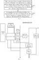
- Fig. 1 illustrates a schematic circuit diagram of an electronic device 100.
- the electronic device 100 supports charging in the high voltage charging mode.
- the electronic device 100 may include a charging interface 110, a battery 140, and a charging circuit 120 and a control circuit 130 disposed between the charging interface 110 and the battery 140.
- the charging circuit 120 can be referred to as a BUCK circuit, mainly including a MOSFET (Metal-Oxide-Semiconductor Field Effect Transistor) transistor 1 (MOSFET-1), a MOSFET transistor 2 (MOSFET-2), an inductor and a capacitor, in which the MOSFET-1 and the MOSFET-2 are turned on alternately during the charging.
- MOSFET Metal-Oxide-Semiconductor Field Effect Transistor
- Fig. 2 illustrates a schematic circuit diagram of another electronic device 200.
- the electronic device 200 may include a charging interface 210, a battery 240, and a charging circuit 220 and a control circuit 230 disposed between the charging interface 210 and the battery 240.
- the electronic device 200 supports charging in the low voltage charging mode.
- the charging circuit 220 includes a MOSFET transistor 3 (MOSFET-3) and a capacitor, in which the MOSFET-3 is always turned on during the charging.
- MOSFET-3 MOSFET transistor 3
- the electronic device in Fig. 1 can only support the high voltage charging mode, and the electronic device in Fig. 2 can only support the low voltage charging mode. Therefore, the electronic device can be charged only when it is coupled with a power adapter matched with the charging mode which it supports, thus limiting the charging scene of the electronic device and degrading the user experience.
- Embodiments of the present disclosure provide a charge control method and device and an electronic device, which may not only support charging in a high voltage charging mode but also support charging in a low voltage charging mode.
- embodiments of the present disclosure provide a charge control method.
- the method is applied in an electronic device, the electronic device includes a charging interface, a charging circuit and a battery coupled in series, and the method includes: when a charging device is coupled with the charging interface, determining, by a charge control device, a charging mode supported by the charging device as a high voltage charging mode or a low voltage charging mode, in which a charging voltage of the high voltage charging mode is greater than a charging voltage of the low voltage charging mode; and controlling the charging circuit by the charge control device according to the charging mode supported by the charging device, such that the charging circuit charges the battery in the charging mode supported by the charging device.
- the charging circuit includes a first switch element and a second switch element; controlling the charging circuit by the charge control device according to the charging mode supported by the charging device, such that the charging circuit charges the battery in the charging mode supported by the charging device, includes: if the charging mode supported by the charging device is the low voltage charging mode, controlling the first switch element to switch on, and controlling the second switch element to switch off.
- the charging circuit includes a first switch element and a second switch element; controlling the charging circuit by the charge control device according to the charging mode supported by the charging device, such that the charging circuit charges the battery in the charging mode supported by the charging device, includes: if the charging mode supported by the charging device is the high voltage charging mode, controlling the first switch element and the second switch element to switch on alternately.
- a first end of the charge control device is coupled with a grid of the first switch element, a second end of the charge control device is coupled with a grid of the second switch element; a source of the first switch element is coupled with a drain of the second switch element; a drain of the first switch element is coupled with a power line of the charging interface, a source of the second switch element is grounded; the charging circuit further includes an inductance element and a capacitance element, in which a first end of the inductance element is coupled with the source of the first switch element and the drain of the second switch element respectively; a second end of the inductance element is coupled with a first end of the capacitance element and a first end of the battery respectively; a second end of the capacitance element is coupled with a second end of the battery and grounded.
- the first switch element is a first MOSFET transistor
- the second switch element is a second MOSFET transistor
- a charge control device is provided.
- the device is applied in an electronic device, the electronic device includes a charging interface, a charging circuit and a battery coupled in series, and the device includes: a determining unit, configured to determine a charging mode supported by a charging device as a high voltage charging mode or a low voltage charging mode when the charging device is coupled with the charging interface, in which a charging voltage of the high voltage charging mode is greater than a charging voltage of the low voltage charging mode; a control unit, configured to control the charging circuit according to the charging mode supported by the charging device and determined by the determining unit, such that the charging circuit charges the battery in the charging mode supported by the charging device.
- the charging circuit includes a first switch element and a second switch element; the control unit is configured to: control the first switch element to switch on and control the second switch element to switch off, if the determining unit determines that charging mode supported by the charging device is the low voltage charging mode.
- the charging circuit includes a first switch element and a second switch element; the control unit is configured to: control the first switch element and the second switch element to switch on alternately, if the determining unit determines that the charging mode supported by the charging device is the high voltage charging mode.
- a first end of the charge control device is coupled with a grid of the first switch element, a second end of the charge control device is coupled with a grid of the second switch element; a source of the first switch element is coupled with a drain of the second switch element; a drain of the first switch element is coupled with a power line of the charging interface, a source of the second switch element is grounded; the charging circuit further includes an inductance element and a capacitance element, in which a first end of the inductance element is coupled with the source of the first switch element and the drain of the second switch element respectively; a second end of the inductance element is coupled with a first end of the capacitance element and a first end of the battery respectively; a second end of the capacitance element is coupled with a second end of the battery and grounded.
- a data line of the charging interface is configured to perform communication between the electronic device and the charging device;
- the determining unit includes: a receiving sub-unit, configured to receive indication information sent by the charging device via the data line of the charging interface, in which the indication information is configured to indicate the charging mode supported by the charging device; and a determining sub-unit, configured to determine the charging mode supported by the charging device as the high voltage charging mode or the low voltage charging mode according to the indication information received by the receiving sub-unit.
- the first switch element is a first MOSFET transistor
- the second switch element is a second MOSFET transistor
- a processor is provided.
- the processor is applied in an electronic device, and the electronic device includes a charging interface, a charging circuit and a battery coupled in series.
- the processor is configured to: determine a charging mode supported by a charging device as a high voltage charging mode or a low voltage charging mode when the charging device is coupled with the charging interface, in which a charging voltage of the high voltage charging mode is greater than a charging voltage of the low voltage charging mode; and control the charging circuit according to the charging mode supported by the charging device, such that the charging circuit charges the battery in the charging mode supported by the charging device.
- the charging circuit includes a first switch element and a second switch element.
- a first end of the processor is coupled with a grid of the first switch element
- a second end of the processor is coupled with a grid of the second switch element
- a source of the first switch element is coupled with a drain of the second switch element
- a drain of the first switch element is coupled with a power line of the charging interface
- source of the second switch element is grounded.
- the processor is configured to control the first switch element to switch on and control the second switch element to switch off, if the charging mode supported by the charging device is the low voltage charging mode.
- the processor is configured to control the first switch element and the second switch element to switch on alternately, if the charging mode supported by the charging device is the high voltage charging mode.
- the first switch element is a first MOSFET transistor
- the second switch element is a second MOSFET transistor
- the charging circuit further includes an inductance element and a capacitance element, in which a first end of the inductance element is coupled with the source of the first switch element and the drain of the second switch element respectively; a second end of the inductance element is coupled with a first end of the capacitance element and a first end of the battery respectively; a second end of the capacitance element is coupled with a second end of the battery and grounded.
- a data line of the charging interface is configured to perform communication between the electronic device and the charging device; the processor is configured to: receive indication information sent by the charging device via the data line of the charging interface, in which the indication information is configured to indicate the charging mode supported by the charging device; and determine the charging mode supported by the charging device as the high voltage charging mode or the low voltage charging mode according to the indication information.
- the charging circuit further includes a first detecting circuit and a second detecting circuit.
- the source of the first switch element is coupled with the power line of the charging interface via the first detecting circuit, and two ends of the first detecting circuit are coupled with a third end and a fourth end of the processor respectively.
- Two ends of the second detecting circuit are coupled with a fifth end and a sixth end of the processor respectively.
- the processor is further configured to: determine by the first detecting circuit a charging parameter input by the power line of the charging interface and determine by the second detecting circuit a charging parameter of the battery, if the charging device supports the high voltage charging mode, in which the charging parameter includes at least one of a voltage and a current; and control the charging circuit according to the charging parameter input by the power line of the charging interface and the charging parameter of the battery, such that the charging circuit charges the battery in the charging mode supported by the charging device.
- the processor is configured to: determine whether the charging is abnormal or whether the battery is fully charged according to the charging parameter input by the power line of the charging interface and the charging parameter of the battery; if it is determined that the charging is abnormal or the battery is fully charged, control the first switch element and the second switch element to switch off, such that the charging device stops charging the battery.
- a computer readable medium configured to store programs that when executed by a processor, cause the processor to perform a method according to the first aspect or any possible implementation of the first aspect.
- an electronic device in a fifth aspect, includes a charging interface, a charging circuit and a battery coupled in series, and the electronic device further includes the charge control device according to the second aspect or any possible implementation of the second aspect.
- inventions of the present disclosure provide an electronic device.
- the electronic device includes a charging interface, a charging circuit and a battery coupled in series, and the electronic device further includes a controller coupled with the charging circuit, and the controller is configured to: determine a charging mode supported by a charging device as a high voltage charging mode or a low voltage charging mode when the charging device is coupled with the charging interface, in which a charging voltage of the high voltage charging mode is greater than a charging voltage of the low voltage charging mode; and control the charging circuit according to the charging mode supported by the charging device, such that the charging circuit charges the battery in the charging mode supported by the charging device.
- the charging circuit includes a first switch element and a second switch element; a first end of the controller is coupled with a grid of the first switch element, a second end of the controller is coupled with a grid of the second switch element, a source of the first switch element is coupled with a drain of the second switch element, a drain of the first switch element is coupled with a power line of the charging interface, and a source of the second switch element is grounded.
- the controller is configured to control the first switch element to switch on and control the second switch element to switch off, if the charging mode supported by the charging device is the low voltage charging mode.
- the controller is configured to control the first switch element and the second switch element to switch on alternately, if the charging mode supported by the charging device is the high voltage charging mode.
- the first switch element is a first MOSFET transistor
- the second switch element is a second MOSFET transistor
- the charging circuit further includes an inductance element and a capacitance element, in which a first end of the inductance element is coupled with the source of the first switch element and the drain of the second switch element respectively; a second end of the inductance element is coupled with a first end of the capacitance element and a first end of the battery respectively; a second end of the capacitance element is coupled with a second end of the battery and grounded.
- the controller is further coupled with a data line of the charging interface, in which the data line of the charging interface is configured to perform communication between the electronic device and the charging device.
- the processor is configured to: receive indication information sent by the charging device via the data line of the charging interface, in which the indication information is configured to indicate the charging mode supported by the charging device; and determine the charging mode supported by the charging device as the high voltage charging mode or the low voltage charging mode according to the indication information.
- the charging circuit further includes a first detecting circuit and a second detecting circuit.
- the source of the first switch element is coupled with the power line of the charging interface via the first detecting circuit, and two ends of the first detecting circuit are coupled with a third end and a fourth end of the controller respectively.
- Two ends of the second detecting circuit are coupled with a fifth end and a sixth end of the controller respectively.
- the controller is further configured to: determine by the first detecting circuit a charging parameter input by the power line of the charging interface and determine by the second detecting circuit a charging parameter of the battery, if the charging device supports the high voltage charging mode, in which the charging parameter includes at least one of a voltage and a current; and control the charging circuit according to the charging parameter input by the power line of the charging interface and the charging parameter of the battery, such that the charging circuit charges the battery in the charging mode supported by the charging device.
- the controller is configured to: determine whether the charging is abnormal or whether the battery is fully charged according to the charging parameter input by the power line of the charging interface and the charging parameter of the battery; if it is determined that the charging is abnormal or the battery is fully charged, control the first switch element and the second switch element to switch off, such that the charging device stops charging the battery.
- the charging circuit can work in the charging mode supported by the charging device, such that both the charging in the high voltage charging mode and the charging in the low voltage charging mode can be supported, thereby being suitable for various scenes of different charging devices, and improving user experience.
- Fig. 3 is a schematic circuit diagram of an electronic device 300 according to an embodiment of the present disclosure.
- the electronic device 300 includes a charging interface 310, a charging circuit 320 and a battery 330.
- the charging interface 310 can be coupled with a charging device.
- the charging device may be any device which can charge the electronic device via the charging interface 310, such as a power adapter, a charge pal, a portable power source, and a personal computer, and the present disclosure is not limited thereto.
- the charging circuit 320 can be configured to receive the charging current transmitted by the charging device via the charging interface 310 and to charge the battery 330 according to the charging current.
- the battery 330 can be a lithium battery or any other type of battery, which is not limited in embodiments of the present disclosure.
- the charging interface 310 can be a USB (Universal Serial Bus) interface, for example, a common USB interface or a micro USB interface, which is not limited in embodiments of the present disclosure.
- the charging interface 310 can include a power line and a data line.
- the power line of the charging interface 310 can be a VBus line and/or a ground line in the USB interface, and specifically, can be configured to charge the electronic device.
- the data line of the charging interface 310 can be a D+ line and/or a D- line in the USB interface, and specifically, can be configured to perform bidirectional communication between the electronic device and the charging device.
- the bidirectional communication can refer to an information interaction between the electronic device and the charging device, but the embodiments of the present disclosure are not limited thereto.
- the electronic device can support a common charging mode and a quick charging mode, in which the charging current of the quick charging mode is greater than the charging current of the common charging mode, for example, the charging current of the common charging mode is generally less than 2.5A, and the charging current of the quick charging mode can be greater than 3A, but the embodiments of the present disclosure are not limited thereto.
- the electronic device can support a high voltage charging mode and a low voltage charging mode, in which the charging voltage of the high voltage charging mode is greater than the charging voltage of the low voltage charging mode.
- the charging voltage of the high voltage charging mode can be greater than a standard voltage (5V), and the charging voltage of the low voltage charging mode can be less than the standard voltage, but embodiments of the present disclosure are not limited thereto.
- the charging current of the high voltage charging mode and the low voltage charging mode is not limited in embodiments of the present disclosure.
- the high voltage charging mode can be a high-voltage quick charging mode, and can also be a high-voltage common charging mode.
- the low voltage charging mode can be a low-voltage quick charging mode, and can also be a low-voltage common charging mode.
- Fig. 4 is a flow chart of a charge control method 400 according to an embodiment of the present disclosure.
- the method 400 can be applied in an electronic device.
- the electronic device can be the electronic device 300 illustrated in Fig. 3 , but embodiments of the present disclosure are not limited thereto.
- the method 400 can be executed by one or more components in the electronic device, for example, the method 400 can be executed by a processor or a control circuit or a controller in the electronic device.
- the charge control method 400 is executed by a charge control device as an example, in which the charge control device can be disposed in the electronic device, for example, the electronic device can include a control circuit, and the control circuit includes the charge control device, but embodiments of the present disclosure are not limited thereto.
- the method 400 includes following acts.
- a charging mode supported by the charging device is determined as the high voltage charging mode or the low voltage charging mode, in which the charging voltage of the high voltage charging mode is greater than the charging voltage of the low voltage charging mode.
- the charging circuit is controlled according to the charging mode supported by the charging device, such that the charging circuit charges the battery in the charging mode supported by the charging device.
- the charging circuit can work in the charging mode supported by the charging device, such that both the charging in the high voltage charging mode and the charging in the low voltage charging mode can be supported, thereby being suitable for various scenes of different charging devices, and improving user experience.
- the charge control device can further detect whether the charging interface is coupled with the charging device, and determine the charging mode supported by the charging device when determining that the charging interface is coupled with the charging device, but embodiments of the present disclosure are not limited thereto.
- the charge control device can determine the charging mode supported by the charging device as the high voltage charging mode or the low voltage charging mode, for example, determine the charging mode supported by the charging device as the high-voltage quick charging mode or the low-voltage quick charging mode, but embodiments of the present disclosure are not limited thereto.
- the charge control device can determine the charging mode supported by the charging device in many ways.
- the charge control device can communicate with the charging device via the data line of the charging interface, so as to determine the charging mode supported by the charging device.
- determining the charging mode supported by the charging device as the high voltage charging mode or the low voltage charging mode includes:
- the indication information can include information on protocol version supported by the charging device (protocol version information).
- the charge control device can determine the charging mode supported by the charging device as the high voltage charging mode or the low voltage charging mode according to the protocol version information.
- the indication information can also include any other information which can be used by the charge control device for determining the charging mode supported by the charging device, which is not limited in embodiments of the present disclosure.
- the charging device can actively send the indication information to the charge control device via the data line of the charging interface.
- the charge control device sends second indication information to the charging device via the data line of the charging interface when the charge control device detects that the charging device is coupled with the charging interface, in which the second indication information is configured to query the charging mode supported by the charging device. Accordingly, the charging device sends the indication information to the charge control device via the data line of the charging interface according to the second indication information after receiving the second indication information sent by the charge control device.
- the data line of the charging interface can be a D+ line and/or a D- line of the USB interface, which is not limited in embodiments of the present disclosure.
- the charge control device can control the working mode of the charging circuit, such that the charging circuit works in the charging mode supported by the charging device.
- the charging circuit 320 can specifically include a first switch element 321 and a second switch element 322.
- a first end of the charge control device can be coupled with a grid of the first switch element 321, a second end of the charge control device can be coupled with a grid of the second switch element 322, that is, the first end of the charge control device can be coupled with the grid of first switch element 321 directly or via other elements, and the second end of the charge control device can be coupled with the grid of the second switch element 322 directly or via other elements.
- a source of the first switch element 321 can be coupled with a drain of the second switch element 322, a drain of the first switch element 321 can be coupled with the power line of the charging interface 310 directly or indirectly, and a source of the second switch element 322 can be grounded.
- the charge control device can control the charging circuit by controlling the first switch element and the second switch element, but the present disclosure is not limited thereto.
- the first switch element and/or the second switch element can be a MOSFET transistor, a relay or a triode, which is not limited in embodiments of the present disclosure.
- controlling the charging circuit according to the charging mode supported by the charging device such that the charging circuit charges the battery in the charging mode supported by the charging device includes:
- the charge control device can control the first switch element to be always turned on during the charging, and control the second switch element to be always turned off during the charging, such that the charging current provided by the charging device is transmitted to the battery via the first switch element of the charging circuit.
- the charging circuit can be in the bypass mode, which is not limited in the present disclosure.
- controlling the charging circuit according to the charging mode supported by the charging device such that the charging circuit charges the battery in the charging mode supported by the charging device includes:
- the charge control device can control the first switch element to be in a switch-on state and in a switch-off state alternately during the charging, and control the second switch element to be also in the switch-on state and in the switch-off state alternately during the charging, in which, at a same time point, one of the first switch element and the second switch element is in the switch-on state, and the other one is in the switch-off state, such that the first switch element and the second switch element are in the switch-on state alternately.
- the charge control device can control the first switch element to be in the switch-on state within a first time period, and control the second switch element to be in the switch-off state within the first time period; control the first switch element to be in the switch-off state within a second time period, and control the second switch element to be in the switch-on state within the second time period, in which the second time period can be immediately after the first time period.
- the charging circuit can be in the buck mode, which is not limited in the present disclosure.
- the charging circuit 320 can further include an inductance element 323 and a capacitance element 324.
- a first end of the inductance element 323 can be coupled with the source of the first switch element and the drain of the second switch element respectively.
- a second end of the inductance element 323 can be coupled with a first end of the capacitance element 324 and a first end of the battery 330 respectively.
- a second end of the capacitance element 324 is coupled with a second end of the battery 330 and is grounded.
- Fig. 5 schematically illustrates that the first end of the inductance element 323 is coupled with the source of the first switch element 321 and the drain of the second switch element 322 directly.
- the second end of the inductance element 323 is coupled with the first end of the capacitance element 324 and the first end of the battery 330 directly, but the present disclosure is not limited thereto.
- the capacitance element can be a capacitor configured with a PCB (Printed Circuit Board) or a capacitor configured with a FPC (Flexible Printed Circuit).
- PCB Print Circuit Board
- FPC Flexible Printed Circuit
- the capacitor configured with the PCB can be a capacitor configured specially using a PCB and a copper foil thereon
- the capacitor configured with the FPC can be a capacitor designed specially using the FPC.
- the capacitor configured with the PCB and the capacitor configured with the FPC mainly have advantages in that they can be designed as any shape, any size, and any thickness, and can be designed randomly according to the structure and shape of the electronic device such as the mobile phone.
- the size, shape or thickness of the capacitor in the capacity coupler is designed based on the structure of the electronic device.
- the capacitance element 324 and the inductance element 323 store energy.
- the first switch element 321 can receive the charging current transmitted by the charging device via the power line of the charging interface 310, and transmit the received charging current to the inductance element 323, and the inductance element 323 can transmit the received charging current to the capacitance element 324 and the battery 330 respectively, such that the battery 330 is charged.
- the inductance element 323 and the capacitance element 324 release energy.
- the inductance element 323 transmits current to the capacitance element 324 and the battery 330 respectively, and the capacitance element 324 transmits current to the battery 330, and transmits current to the second switch element 322 via the ground, which is not limited in the present disclosure.
- the charge control device can control the charging current and voltage during the charging.
- the charge control device can detect the voltage and/or current of the charging circuit, and control the current and/or voltage of the charging circuit according to the detection result.
- the charging circuit 320 further includes a first detecting circuit 325 and a second detecting circuit 326.
- the source of the first switch element 621 is coupled with the power line of the charging interface 510 via the first detecting circuit 325, and two ends of the first detecting circuit 325 are coupled with a third end and a fourth end of the charge control device respectively.
- the second end of the inductance element is coupled with the first end of the battery via the second detecting circuit, and two ends of the second detecting circuit 326 are coupled with a fifth end and a sixth end of the charge control device respectively.
- a seventh end of the charge control device can be grounded, and the first detecting circuit 325 and/or the second detecting circuit 326 can include a current detecting resistor with a small resistance and/or other elements, which is not limited in the present disclosure.
- controlling the charging circuit according to the charging mode supported by the charging device such that the charging circuit charges the battery in the charging mode supported by the charging device includes:
- the charge control device can determine the voltage V BUS and/or the current I BUS input by the power line of the charging interface by detecting the voltage across the first detecting circuit, and can determine the voltage V BAT and/or the current I BAT of the battery by detecting the voltage across the second detecting circuit.
- the charge control device can control the charging circuit according to at least one of V BUS, I BUS , V BAT and I BAT , such that charging the battery in the high voltage charging mode is realized.
- the charge control device can control the switch-on duration of the first switch element and the switch-on duration of the second switch element, for example, control the switch frequency and duty ratio of each of the first switch element and the second switch element, in which the switch frequency is used to represent the number of state switching cycles included in an unit time, and the duty ratio is used to represent a ratio of the duration in which the switch element is in the switch-on state to one state switching cycle.
- the present disclosure is not limited thereto.
- the charging device when the charging device supports the low voltage working mode, the charging device can control the charging current and/or voltage, so as to ensure that the charging current is constant; or the charge control device can communicate with the charging device and control the voltage and current during the charging, which is not limited in the present disclosure.
- controlling the charging circuit by the charge control device according to the charging parameter input by the power line of the charging interface and the charging parameter of the battery such that the charging circuit charges the battery in the charging mode supported by the charging device includes:
- the charge control device can control the first switch element to switch to the switch-off state from the switch-on state, such that the charging device stops charging the battery, while the present disclosure is not limited thereto.
- serial numbers of the above processes do not mean an execution order, and the execution order of respective processes is determined according to the functions and internal logic thereof, which shall not be constructed to limit the implementation of embodiments of the present disclosure.
- Fig. 6 illustrates a charge control device 500 according to an embodiment of the present disclosure.
- the device 500 can be applied in an electronic device including a charging interface, a charging circuit and a battery coupled in series, in which the charging interface can be a USB interface, which is not limited in the present disclosure.
- the device 500 can be applied in the electronic device, which is not limited in the present disclosure.
- the device 500 includes a determining unit 510 and a control unit 520.
- the determining unit 510 is configured to determine a charging mode supported by a charging device as a high voltage charging mode or a low voltage charging mode when the charging device is coupled with the charging interface, in which a charging voltage of the high voltage charging mode is greater than a charging voltage of the low voltage charging mode.
- the control unit 520 is configured to control the charging circuit according to the charging mode supported by the charging device and determined by the determining unit 510, such that the charging circuit charges the battery in the charging mode supported by the charging device.
- the determining unit 510 can further detect whether the charging interface is coupled with the charging device, and determine the charging mode supported by the charging device when determining that the charging interface is coupled with the charging device, while the present disclosure is not limited thereto.
- the determining unit 510 can determine the charging mode supported by the charging device as the high voltage charging mode or the low voltage charging mode, for example, determine the charging mode supported by the charging device as the high-voltage quick charging mode or the low-voltage quick charging mode, which is not limited in the present disclosure.
- the charge control device can be coupled with the charging circuit, for controlling the charging circuit.
- the charging circuit can include a first switch element and a second switch element.
- a first end of the charge control device can be coupled with a grid of the first switch element
- a second end of the charge control device can be coupled with a grid of the second switch element
- a source of the first switch element can be coupled with a drain of the second switch element
- a drain of the first switch element can be coupled with a power line of the charging interface directly or indirectly
- a source of the second switch element can be grounded.
- the device can be coupled with the charging circuit in other ways, which is not limited in the present disclosure.
- the first switch element is a first MOSFET transistor
- the second switch element is a second MOSFET transistor
- the first switch element and/or the second switch element can be a triode or a relay, which is not limited in the present disclosure.
- the charging circuit further includes an inductance element and a capacitance element.
- a first end of the inductance element is coupled with the source of the first switch element and the drain of the second switch element respectively.
- a second end of the inductance element is coupled with a first end of the capacitance element and a first end of the battery respectively.
- a second end of the capacitance element is coupled with a second end of the battery and grounded.
- control unit 520 is configured to control the first switch element to switch on and control the second switch element to switch off, if the determining unit 510 determines that the charging mode supported by the charging device is the low voltage charging mode.
- control unit 520 can be configured to control the first switch element to be always switched on during the charging, and to control the second switch element to be always switched off during the charging, such that the charging current provided by the charging device is transmitted to the battery via the first switch element of the charging circuit.
- the charging circuit may be in the bypass mode, which is not limited in the present disclosure.
- control unit 520 is configured to control the first switch element and the second switch element to switch on alternately, if the determining unit 510 determines that the charging mode supported by the charging device is the high voltage charging mode.
- control unit 520 can control the first switch element to be in a switch-on state and in a switch-off state alternately during the charging, and control the second switch element to be also in the switch-on state and in the switch-off state alternately during the charging, in which, at a same time point, one of the first switch element and the second switch element is in the switch-on state, and the other one is in the switch-off state, such that the first switch element and the second switch element are in the switch-on state alternately.
- the charging circuit can be in the buck mode, which is not limited in the present disclosure.
- the device 500 can further be coupled with a data line of the charging interface, in which the data line of the charging interface is configured to perform communication between the electronic device and the charging device.
- the determining unit 510 includes a receiving sub-unit and a determining sub-unit.
- the receiving sub-unit is configured to receive, via the data line of the charging interface, indication information sent by the charging device, in which the indication information is configured to indicate the charging mode supported by the charging device.
- the determining sub-unit is configured to determine the charging mode supported by the charging device as the high voltage charging mode or the low voltage charging mode according to the indication information received by the receiving sub-unit.
- the determining unit 510 can further determine the charging mode supported by the charging device in other ways, which is not limited in the present disclosure.
- the charging circuit further includes a first detecting circuit and a second detecting circuit.
- the source of the first switch element is specifically coupled with the power line of the charging interface via the first detecting circuit, and two ends of the first detecting circuit are coupled with a third end and a fourth end of the charge control device respectively.
- Two ends of the second detecting circuit are coupled with a fifth end and a sixth end of the charge control device respectively.
- the first detecting circuit and/or the second detecting circuit can include a current detecting resistor with a small resistance and/or other elements, which is not limited in the present disclosure.
- the control unit 520 can be further configured to: determine via the first detecting circuit, a charging parameter input by the power line of the charging interface, and determine via the second detecting circuit, a charging parameter of the battery, in which the charging parameter can include at least one of the current and the voltage; and control the charging circuit according to the charging parameter input by the power line of the charging interface and the charging parameter of the battery, such that the charging circuit charges the battery in the charging mode supported by the charging device.
- control unit 520 can be configured to: determine whether the charging is abnormal or whether the battery is fully charged according to the charging parameter input by the power line of the charging interface and the charging parameter of the battery; if it is determined that the charging is abnormal or the battery is fully charged, control the first switch element and the second switch element to switch off, such that the charging process is terminated.
- the charging circuit can work in the charging mode supported by the charging device, such that both the charging in the high voltage charging mode and the charging in the low voltage charging mode can be supported, thereby being suitable for various scenes of different charging devices, and improving user experience.
- Embodiments of the present disclosure further provide a processor.
- the processor can be applied in an electronic device including a charging interface, a charging circuit and a battery coupled in series, in which the charging interface can be a USB interface, which is not limited in the present disclosure.
- the processor can be applied in the electronic device, which is not limited in the present disclosure.
- the processor is configured to:
- the processor can further detect whether the charging interface is coupled with the charging device, and determine the charging mode supported by the charging device when determining that the charging interface is coupled with the charging device, while the present disclosure is not limited thereto.
- the processor can determine the charging mode supported by the charging device as the high voltage charging mode or the low voltage charging mode, for example, determine the charging mode supported by the charging device as the high-voltage quick charging mode or the low-voltage quick charging mode, which is not limited in the present disclosure.
- the processor can be coupled with the charging circuit, for controlling the charging circuit.
- the charging circuit can include a first switch element and a second switch element.
- a first end of the processor can be coupled with a grid of the first switch element
- a second end of the processor can be coupled with a grid of the second switch element
- a source of the first switch element can be coupled with a drain of the second switch element
- a drain of the first switch element can be coupled with a power line of the charging interface directly or indirectly
- a source of the second switch element can be grounded.
- the processor can be coupled with the charging circuit in other ways, which is not limited in the present disclosure.
- the first switch element is a first MOSFET transistor
- the second switch element is a second MOSFET transistor
- the first switch element and/or the second switch element can be a triode or a relay, which is not limited in the present disclosure.
- the charging circuit further includes an inductance element and a capacitance element.
- a first end of the inductance element is coupled with the source of the first switch element and the drain of the second switch element respectively.
- a second end of the inductance element is coupled with a first end of the capacitance element and a first end of the battery respectively.
- a second end of the capacitance element is coupled with a second end of the battery and grounded.
- the processor is configured to control the first switch element to switch on and control the second switch element to switch off, if the charging mode supported by the charging device is the low voltage charging mode.
- the processor can be configured to control the first switch element to be always switched on during the charging, and to control the second switch element to be always switched off during the charging, such that the charging current provided by the charging device is transmitted to the battery via the first switch element of the charging circuit.
- the charging circuit can be in the bypass mode, which is not limited in the present disclosure.
- the processor is configured to control the first switch element and the second switch element to switch on alternately, if the charging mode supported by the charging device is the high voltage charging mode.
- the processor can control the first switch element to be in a switch-on state and in a switch-off state alternately during the charging, and control the second switch element to be also in the switch-on state and in the switch-off state alternately during the charging, in which, at a same time point, one of the first switch element and the second switch element is in the switch-on state, and the other one is in the switch-off state, such that the first switch element and the second switch element are in the switch-on state alternately.
- the charging circuit can be in the buck mode, which is not limited in the present disclosure.
- the processor can further be coupled with a data line of the charging interface, in which the data line of the charging interface is configured to perform communication between the electronic device and the charging device.
- the processor is configured to: receive via the data line of the charging interface indication information sent by the charging device, in which the indication information is configured to indicate the charging mode supported by the charging device; determine the charging mode supported by the charging device as the high voltage charging mode or the low voltage charging mode according to the indication information.
- the processor can also determine the charging mode supported by the charging device in other ways, which is not limited in the present disclosure.
- the charging circuit further includes a first detecting circuit and a second detecting circuit.
- the source of the first switch element is specifically coupled with the power line of the charging interface via the first detecting circuit, and two ends of the first detecting circuit are coupled with a third end and a fourth end of the processor respectively.
- Two ends of the second detecting circuit are coupled with a fifth end and a sixth end of the processor respectively.
- the first detecting circuit and/or the second detecting circuit can include a current detecting resistor with a small resistance and/or other elements, which is not limited in the present disclosure.
- the processor can be further configured to: determine via the first detecting circuit, a charging parameter input by the power line of the charging interface, and determine via the second detecting circuit, a charging parameter of the battery, in which the charging parameter can include at least one of the current and the voltage; and control the charging circuit according to the charging parameter input by the power line of the charging interface and the charging parameter of the battery, such that the charging circuit charges the battery in the charging mode supported by the charging device.
- the processor can be configured to: determine whether the charging is abnormal or whether the battery is fully charged according to the charging parameter input by the power line of the charging interface and the charging parameter of the battery; if it is determined that the charging is abnormal or the battery is fully charged, control the first switch element and the second switch element to switch off, such that the charging device stops charging the battery.
- the charging circuit can work in the charging mode supported by the charging device, such that both the charging in the high voltage charging mode and the charging in the low voltage charging mode can be supported, thereby being suitable for various scenes of different charging devices, and improving user experience.
- Embodiments of the present disclosure further provide a computer readable storage medium configured to store programs and/or at least one instruction executable by the processor in the above embodiment.
- the processor executes the programs and/or at least one instruction, it execute respective processes and/or steps described above, for example, the processor can be the processor described above, which is not limited in the present disclosure.
- Embodiments of the present disclosure further provide an electronic device.
- the electronic device can include a memory and a processor, in which the memory is configured to store programs and/or at least one instruction, and the processor can be configured to execute the programs and/or at least one instruction stored in the memory, so as to execute respective processes and/or steps described above, which is not limited in the present disclosure.
- Fig. 7 illustrates another electronic device 600 provided by embodiments of the present disclosure.
- the electronic device 600 includes a charging interface 610, a charging circuit 620 and a battery 630 coupled in series, and the electronic device 600 further includes a controller 640 coupled with the charging circuit 620.
- the controller 640 is configured to: determine a charging mode supported by a charging device as a high voltage charging mode or a low voltage charging mode when the charging device is coupled with the charging interface 610, in which a charging voltage of the high voltage charging mode is greater than the charging voltage of the low voltage charging mode; control the charging circuit 620 according to the charging mode supported by the charging device, such that the charging circuit 620 charges the battery 630 in the charging mode supported by the charging device.
- controller 640 can be the charge control device 500 or the processor described above, which is not limited in the present disclosure.
- the electronic device 600 can include a control circuit, and the controller 640 can be located in the control circuit.
- the control circuit can further include other elements, which is not limited in the present disclosure.
- the charging circuit 620 includes a first switch element 621 and a second switch element 622.
- a first end of the controller 640 can be coupled with a grid of the first switch element 621
- a second end of the controller 640 can be coupled with a grid of the second switch element 622.
- a source of the first switch element 621 can be coupled with a drain of the second switch element 622
- a drain of the first switch element 621 can be coupled with the power line of the charging interface 610 directly or indirectly.
- a source of the second switch element 622 can be grounded.
- the controller 640 can also be coupled with the charging circuit 620 in other ways, which is not limited in the present disclosure.
- the first switch element 621 is a first MOSFET transistor
- the second switch element 622 is a second MOSFET transistor.
- the first switch element 621 and/or the second switch element 622 can be a triode or a relay, which is not limited in the present disclosure.
- the charging circuit 620 further includes an inductance element 623 and a capacitance element 624.
- a first end of the inductance element 623 is coupled with the source of the first switch element 621 and the drain of the second switch element 622 respectively.
- a second end of the inductance element 623 is coupled with a first end of the capacitance element 624 and a first end of the battery 630 respectively.
- a second end of the capacitance element 624 is coupled with a second end of the battery 630 and grounded.
- the controller 640 is configured to control the first switch element 621 to switch on and control the second switch element 622 to switch off, if the charging mode supported by the charging device is the low voltage charging mode.
- the controller 640 can be configured to control the first switch element 621 to be always switched on during the charging, and to control the second switch element 622 to be always switched off during the charging, such that the charging current provided by the charging device is transmitted to the battery 630 via the first switch element 621 of the charging circuit 620.
- the charging circuit 620 can be in the bypass mode, which is not limited in the present disclosure.
- the controller 640 is configured to control the first switch element 621 and the second switch element 622 to switch on alternately, if the charging mode supported by the charging device is the high voltage charging mode.
- the controller 640 can control the first switch element 621 to be in a switch-on state and in a switch-off state alternately during the charging, and control the second switch element 622 to be also in the switch-on state and in the switch-off state alternately during the charging, in which, at a same time point, one of the first switch element 621 and the second switch element 622 is in the switch-on state, and the other one is in the switch-off state, such that the first switch element 621 and the second switch element 622 are in the switch-on state alternately.
- the charging circuit 620 can be in the buck mode, which is not limited in the present disclosure.
- the controller 640 can further be coupled with a data line of the charging interface 610, in which the data line of the charging interface 610 is configured to perform communication between the electronic device and the charging device.
- the controller 640 is configured to: receive indication information sent by the charging device via the data line of the charging interface 610, in which the indication information is configured to indicate the charging mode supported by the charging device; determine the charging mode supported by the charging device as the high voltage charging mode or the low voltage charging mode according to the indication information.
- the controller 640 can also determine the charging mode supported by the charging device in other ways, which is not limited in the present disclosure.
- the charging circuit 620 further includes a first detecting circuit 625 and a second detecting circuit 626.
- the source of the first switch element 621 is specifically coupled with the power line of the charging interface 610 via the first detecting circuit 625, and two ends of the first detecting circuit 625 are coupled with a third end and a fourth end of the controller respectively.
- Two ends of the second detecting circuit 626 are coupled with a fifth end and a sixth end of the controller respectively.
- the first detecting circuit 625 and/or the second detecting circuit 626 can include a current detecting resistor with a small resistance and/or other elements, in which Fig. 8 schematically illustrates that the first detecting circuit is a current detecting resistor and the second detecting circuit is a current detecting resistor, which is not limited in the present disclosure.
- the controller 640 can be further configured to: determine via the first detecting circuit 625, a charging parameter input by the power line of the charging interface 610, and determine via the second detecting circuit 626, a charging parameter of the battery 630, in which the charging parameter can include at least one of the current and the voltage; and control the charging circuit 620 according to the charging parameter input by the power line of the charging interface 610 and the charging parameter of the battery 630, such that the charging circuit 620 charges the battery 630 in the charging mode supported by the charging device.
- the controller 640 can be configured to: determine whether the charging is abnormal or whether the battery 630 is fully charged according to the charging parameter input by the power line of the charging interface 610 and the charging parameter of the battery 630; if it is determined that the charging is abnormal or the battery 630 is fully charged, control the first switch element 621 and the second switch element 622 to switch off, such that the charging process is terminated.
- the same charging circuit can not only charge the battery in the high voltage charging mode, but can also charge the battery in the low voltage charging mode, without the need of adding a third switch element and related circuit structure, which is simple in the circuit structure, and is simple to implement, thereby saving cost of the device.
- a connected with B may refer to that A is coupled to B, and may refer to that A is directly connected to B, or A is indirectly connected to B (i.e., A is connected with B via one or more intermediate elements), which is not limited in the present disclosure.
- the electronic device can be any terminal device including a battery and capable of charging the battery via a charging interface, such as a mobile phone, a tablet personal computer, a media player, a smart TV, a laptop computer, a personal digital assistant, a mobile internet device, a wearable device like a smart watch, which is not limited in the present disclosure.
- a charging interface such as a mobile phone, a tablet personal computer, a media player, a smart TV, a laptop computer, a personal digital assistant, a mobile internet device, a wearable device like a smart watch, which is not limited in the present disclosure.
- the processor may be a CPU (Central Processing Unit), or any other general processor, DSP (Digital Signal Processor), ASIC (Application Specific Integrated Circuit), FPGA (Field Programmable Gate Array), or any other programmable logic element, separate gate, or transistor logic device or separate hardware component, etc.
- the general processor may be a microprocessor, or the processor may also be any conventional processor.
- the memory may include a read-only memory and a random access memory, and provide instructions and data to the processor.
- a part of the memory may also include a non-transitory random access memory.
- the memory may also store the information regarding the device type.
- the system, devices and method disclosed in several embodiments provided by the present disclosure can be realized in any other manner.
- the device embodiments described above can be merely exemplary, for example, the units are just divided according to logic functions. In practical implementation, the units can be divided in other manners, for example, multiple units or components can be combined or integrated into another system, or some features can be omitted or not executed.
- the mutual coupling or direct coupling or communication connection described or discussed can be via some interfaces, and indirect coupling or communication connection between devices or units may be electrical, mechanical or of other forms.
- the units illustrated as separate components can be or not be separated physically, and components described as units can be or not be physical units, i.e., can be located at one place, or can be distributed onto multiple network units. It is possible to select some or all of the units according to actual needs, for realizing the objective of embodiments of the present disclosure.
- respective functional units in respective embodiments of the present disclosure can be integrated into one processing unit, or can be present as separate physical entities. It is also possible that two or more than two units are integrated into one unit.
- the functions are realized in form of functional software units and are sold or used as separate products, they can be stored in a computer readable storage medium.
- the parts of the technical solutions or the essential parts of the technical solutions i.e. the parts making a contribution to the related art
- the above storage medium may be any medium capable of storing program codes, including a USB flash disk, a mobile hard disk, a Read-Only Memory (ROM), a Random Access Memory (RAM), a disc, or a light disk.
Landscapes
- Engineering & Computer Science (AREA)
- Power Engineering (AREA)
- Charge And Discharge Circuits For Batteries Or The Like (AREA)
Priority Applications (1)
| Application Number | Priority Date | Filing Date | Title |
|---|---|---|---|
| EP21213456.3A EP3985835A1 (de) | 2015-09-22 | 2015-09-22 | Ladesteuerungsverfahren und -vorrichtung sowie elektronische vorrichtung |
Applications Claiming Priority (1)
| Application Number | Priority Date | Filing Date | Title |
|---|---|---|---|
| PCT/CN2015/090271 WO2017049459A1 (zh) | 2015-09-22 | 2015-09-22 | 控制充电的方法和装置以及电子设备 |
Related Child Applications (2)
| Application Number | Title | Priority Date | Filing Date |
|---|---|---|---|
| EP21213456.3A Division-Into EP3985835A1 (de) | 2015-09-22 | 2015-09-22 | Ladesteuerungsverfahren und -vorrichtung sowie elektronische vorrichtung |
| EP21213456.3A Division EP3985835A1 (de) | 2015-09-22 | 2015-09-22 | Ladesteuerungsverfahren und -vorrichtung sowie elektronische vorrichtung |
Publications (3)
| Publication Number | Publication Date |
|---|---|
| EP3200311A1 true EP3200311A1 (de) | 2017-08-02 |
| EP3200311A4 EP3200311A4 (de) | 2018-04-11 |
| EP3200311B1 EP3200311B1 (de) | 2022-01-19 |
Family
ID=56840272
Family Applications (2)
| Application Number | Title | Priority Date | Filing Date |
|---|---|---|---|
| EP15897896.5A Active EP3200311B1 (de) | 2015-09-22 | 2015-09-22 | Ladesteuerungsverfahren und vorrichtung sowie elektronische vorrichtung |
| EP21213456.3A Withdrawn EP3985835A1 (de) | 2015-09-22 | 2015-09-22 | Ladesteuerungsverfahren und -vorrichtung sowie elektronische vorrichtung |
Family Applications After (1)
| Application Number | Title | Priority Date | Filing Date |
|---|---|---|---|
| EP21213456.3A Withdrawn EP3985835A1 (de) | 2015-09-22 | 2015-09-22 | Ladesteuerungsverfahren und -vorrichtung sowie elektronische vorrichtung |
Country Status (9)
| Country | Link |
|---|---|
| US (2) | US10833518B2 (de) |
| EP (2) | EP3200311B1 (de) |
| JP (1) | JP6626882B2 (de) |
| KR (1) | KR101894777B1 (de) |
| CN (2) | CN105934865B (de) |
| AU (1) | AU2015401874B2 (de) |
| SG (1) | SG11201700500WA (de) |
| TW (2) | TWI668936B (de) |
| WO (1) | WO2017049459A1 (de) |
Families Citing this family (16)
| Publication number | Priority date | Publication date | Assignee | Title |
|---|---|---|---|---|
| US10833518B2 (en) * | 2015-09-22 | 2020-11-10 | Guangdong Oppo Mobile Telecommunications Corp., Ltd. | Charge control method and device, and electronic device |
| CN106300555B (zh) * | 2016-10-13 | 2019-04-23 | 深圳市金立通信设备有限公司 | 一种充电电路及其充电方法与终端 |
| CN106787708B (zh) * | 2016-12-06 | 2019-04-19 | 矽力杰半导体技术(杭州)有限公司 | 功率变换器和集成电路 |
| TWI662772B (zh) * | 2018-02-13 | 2019-06-11 | 台達電子工業股份有限公司 | 適配連接線、適配模組及其操作方法 |
| CN109217419B (zh) * | 2018-09-21 | 2021-08-03 | 深圳市奥必赢科技有限公司 | 快速充电系统及方法 |
| US10630082B1 (en) * | 2018-11-06 | 2020-04-21 | Wing Aviation Llc | Power communication to regulate charge of unmanned aerial vehicle |
| EP3902086A4 (de) * | 2018-12-21 | 2022-01-12 | Guangdong Oppo Mobile Telecommunications Corp., Ltd. | Aufladesteuerungsvorrichtung und -verfahren sowie elektronische vorrichtung |
| EP3706282B1 (de) | 2018-12-21 | 2023-04-05 | Guangdong Oppo Mobile Telecommunications Corp., Ltd. | Zu ladende vorrichtung und ladesteuerungsverfahren |
| KR102767967B1 (ko) * | 2019-02-19 | 2025-02-14 | 삼성전자주식회사 | 복수의 배터리들의 충전을 제어하는 방법 및 그 방법을 적용한 전자 장치 |
| KR102651536B1 (ko) | 2019-10-10 | 2024-03-28 | 삼성전자주식회사 | 전자 장치의 배터리 충전 제어 방법 및 그 전자 장치 |
| KR102877560B1 (ko) | 2019-11-26 | 2025-10-28 | 삼성전자주식회사 | 전자 장치 및 이의 충전 방법 |
| US11251645B2 (en) * | 2020-01-24 | 2022-02-15 | Dell Products, L.P. | Multimode USB-C power transmission and conversion supporting improved battery charging |
| EP4187748A4 (de) * | 2020-08-21 | 2023-09-13 | Huawei Technologies Co., Ltd. | Schaltung zur steuerung einer zelle und elektronische vorrichtung |
| CN114825495A (zh) * | 2021-01-22 | 2022-07-29 | 北京小米移动软件有限公司 | 一种充电控制方法、充电控制装置、电子设备及存储介质 |
| KR102434036B1 (ko) * | 2021-06-17 | 2022-08-19 | 삼성전자주식회사 | 보조 전원 장치의 수명을 위한 충전 전압 제어 방법 및 이를 수행하는 스토리지 장치 |
| EP4178068B1 (de) * | 2021-10-29 | 2024-04-17 | Nanjing Chervon Industry Co., Ltd. | Ladevorrichtung |
Family Cites Families (150)
| Publication number | Priority date | Publication date | Assignee | Title |
|---|---|---|---|---|
| US75007A (en) * | 1868-03-03 | Improved tutebe | ||
| US6075340A (en) * | 1985-11-12 | 2000-06-13 | Intermec Ip Corp. | Battery pack having memory |
| JPH06124731A (ja) * | 1992-08-31 | 1994-05-06 | Toshiba Corp | 外部バッテリ接続用アタッチメント、バッテリパック及びバッテリ識別制御方法 |
| US5686808A (en) * | 1995-05-31 | 1997-11-11 | Lutz; Frank T. | Universal battery charger and method |
| US6495992B1 (en) * | 1996-03-26 | 2002-12-17 | Norvik Traction Inc. | Method and apparatus for charging batteries utilizing heterogeneous reaction kinetics |
| JP3580693B2 (ja) * | 1998-03-19 | 2004-10-27 | シャープ株式会社 | チャージ・ポンプ回路 |
| US6275006B1 (en) * | 1998-05-27 | 2001-08-14 | Matsushita Electric Industrial Co., Ltd. | Method for charging secondary battery |
| US6037755A (en) * | 1998-07-07 | 2000-03-14 | Lucent Technologies Inc. | Switching controller for a buck+boost converter and method of operation thereof |
| US6882130B2 (en) * | 2001-04-17 | 2005-04-19 | Matsushita Electric Industrial Co., Ltd. | Battery-driven electronic device and mobile communication apparatus |
| US6765370B2 (en) * | 2002-05-17 | 2004-07-20 | Kyocera Wireless Corp. | System and method for bi-directional power conversion in a portable device |
| CN2606979Y (zh) | 2002-10-29 | 2004-03-17 | 联想(北京)有限公司 | 新型便携式设备智能充电装置 |
| US6819011B2 (en) * | 2002-11-14 | 2004-11-16 | Fyre Storm, Inc. | Switching power converter controller with watchdog timer |
| US7279855B2 (en) * | 2003-04-04 | 2007-10-09 | Hitachi, Ltd. | Electric drive device for vehicle and hybrid engine/motor-type four wheel drive device |
| WO2005013455A1 (en) * | 2003-08-05 | 2005-02-10 | Matsushita Electric Industrial Co., Ltd. | Direct-current power supply and battery-powered electronic apparatus equipped with the power supply |
| JP2007520180A (ja) * | 2003-10-14 | 2007-07-19 | ブラック アンド デッカー インク | 電池パックの障害状態からの保護を提供するべく適合された二次電池、電動工具、充電器、及び電池パック用の保護方法、保護回路、及び保護装置 |
| US7352154B2 (en) * | 2004-01-14 | 2008-04-01 | Vanner, Inc. | Electrical system control for a vehicle |
| US7271568B2 (en) * | 2004-02-11 | 2007-09-18 | Research In Motion Limited | Battery charger for portable devices and related methods |
| US7489109B1 (en) * | 2004-06-23 | 2009-02-10 | Intersil Americas Inc. | Integrated battery charger and system regulator circuit |
| US20060022638A1 (en) * | 2004-07-30 | 2006-02-02 | Akku Power Electronic Co., Ltd. | [multifunctional battery charger] |
| TWI283097B (en) * | 2004-12-31 | 2007-06-21 | Jason Auto Technology Co Ltd | Method and device for battery charger and diagnosis with detectable battery energy barrier |
| SG124315A1 (en) * | 2005-01-31 | 2006-08-30 | Stl Corp | Battery pack |
| WO2006081613A1 (en) * | 2005-02-02 | 2006-08-10 | Cap-Xx Limited | A power supply |
| US7719236B2 (en) * | 2005-02-18 | 2010-05-18 | O2Micro International Limited | Parallel powering of portable electrical devices |
| TWI299228B (en) * | 2005-05-18 | 2008-07-21 | Ite Tech Inc | Power supply conversion circuit and method thereof, and a circuitry incorporating the same |
| US7176667B2 (en) * | 2005-06-20 | 2007-02-13 | Aimtron Technology Corp. | Buck-boost voltage converter |
| WO2007067825A1 (en) * | 2005-12-07 | 2007-06-14 | Advanced Bionics Corporation | Battery protection and zero-volt battery recovery system for an implantable medical device |
| TW200722950A (en) * | 2005-12-14 | 2007-06-16 | Golden Bridge Electech Inc | Power supply and method for detecting and adjusting voltages and currents for supplying power requirement of electronic apparatus |
| US7375491B2 (en) * | 2005-12-16 | 2008-05-20 | Sunjett Corporation | Battery charge circuit with multi-charge stage and method thereof |
| EP1821386A2 (de) * | 2006-02-17 | 2007-08-22 | Power Systems Co., Ltd. | Lade- und Entladevorrichtung für eine Stromquelle des Kondensatorspeichertyps |
| US7605568B2 (en) * | 2006-03-10 | 2009-10-20 | Atmel Corporation | Deep under voltage recovery in a battery pack |
| JP4784490B2 (ja) * | 2006-03-13 | 2011-10-05 | セイコーエプソン株式会社 | 電子機器、その制御方法及びそのプログラム |
| US7432689B2 (en) * | 2006-05-05 | 2008-10-07 | Micrel, Inc. | Buck-boost control logic for PWM regulator |
| WO2008030398A2 (en) * | 2006-09-05 | 2008-03-13 | Summit Microelectronics, Inc | Circuits and methods for controlling power in a battery operated system |
| JP2008136278A (ja) * | 2006-11-27 | 2008-06-12 | Matsushita Electric Works Ltd | 充電器 |
| US7764050B2 (en) * | 2007-01-02 | 2010-07-27 | Intersil Americas Inc. | System and method of charging a battery and power delivery using an adapter and capacitor voltage divider |
| US7750604B2 (en) * | 2007-02-16 | 2010-07-06 | O2Micro, Inc. | Circuits and methods for battery charging |
| US8115454B2 (en) * | 2007-03-26 | 2012-02-14 | The Gillette Company | Battery with an integrated voltage converter having a bypass circuit |
| JP2010521948A (ja) * | 2007-03-26 | 2010-06-24 | ザ ジレット カンパニー | 適応充電装置及び方法 |
| EP1990887A1 (de) * | 2007-05-07 | 2008-11-12 | STMicroelectronics S.r.l. | Leistungsverwaltungseinheit für batteriebetriebene Vorrichtungen |
| FI20075322A0 (fi) * | 2007-05-07 | 2007-05-07 | Nokia Corp | Teholähteitä RF-tehovahvistimelle |
| CN201039411Y (zh) * | 2007-05-18 | 2008-03-19 | 龙旗科技(上海)有限公司 | 一种带有自适应充电装置的移动电话机 |
| US20090015229A1 (en) * | 2007-07-14 | 2009-01-15 | Kotikalapoodi Sridhar V | Bi-directional DC power converter |
| US7863865B2 (en) * | 2007-07-26 | 2011-01-04 | Summit Microelectronics, Inc. | Systems and methods for pulse charging a battery |
| JP5146726B2 (ja) * | 2007-10-25 | 2013-02-20 | 日立工機株式会社 | 充電装置 |
| JP2009136097A (ja) * | 2007-11-30 | 2009-06-18 | Rohm Co Ltd | Dc/dcコンバータおよびその制御回路ならびにそれを利用した電子機器 |
| TWI364154B (en) * | 2008-04-30 | 2012-05-11 | Inventec Appliances Corp | Quick charging handheld device |
| US8139382B2 (en) * | 2008-05-14 | 2012-03-20 | National Semiconductor Corporation | System and method for integrating local maximum power point tracking into an energy generating system having centralized maximum power point tracking |
| JP4471024B2 (ja) * | 2008-07-14 | 2010-06-02 | トヨタ自動車株式会社 | Dc−dcコンバータの制御装置 |
| AU2009295283A1 (en) * | 2008-09-29 | 2011-09-15 | Wilson Lee | Multi-chemistry battery charging system and method of identifying and improved charging technique for primary and secondary dry-cell batteries |
| CN101714647B (zh) * | 2008-10-08 | 2012-11-28 | 株式会社牧田 | 电动工具用蓄电池匣以及电动工具 |
| US9933146B2 (en) * | 2009-01-16 | 2018-04-03 | Mag Instrument, Inc. | Portable lighting devices |
| US9247598B2 (en) * | 2009-01-16 | 2016-01-26 | Mag Instrument, Inc. | Portable lighting devices |
| US8058752B2 (en) * | 2009-02-13 | 2011-11-15 | Miasole | Thin-film photovoltaic power element with integrated low-profile high-efficiency DC-DC converter |
| CN101826793B (zh) * | 2009-03-03 | 2012-08-29 | 天津市睿芯隆科技有限公司 | 能源转换控制器 |
| US8536840B2 (en) * | 2009-03-17 | 2013-09-17 | Linear Technology Corporation | Bidirectional power converters |
| CN101854067A (zh) * | 2009-04-01 | 2010-10-06 | 深圳富泰宏精密工业有限公司 | 电子装置及其安全充电的方法 |
| US8598734B2 (en) * | 2009-05-08 | 2013-12-03 | Toyota Jidosha Kabushiki Kaisha | Power supply system and vehicle equipped with the same |
| US8723489B2 (en) * | 2009-05-28 | 2014-05-13 | Deeya Energy, Inc. | Bi-directional buck-boost circuit |
| US8283896B1 (en) * | 2009-06-03 | 2012-10-09 | Polarity, Inc. | Method and system for charging and discharging high-voltage energy storage devices |
| TWI389412B (zh) * | 2009-09-08 | 2013-03-11 | 新普科技股份有限公司 | 充放電保護電路及充電保護方法 |
| US9054549B2 (en) * | 2010-02-23 | 2015-06-09 | Maxim Integrated Products, Inc. | Circuit topology for regulating power from low capacity battery cells |
| US20110234151A1 (en) | 2010-03-26 | 2011-09-29 | Uan-Zo-Li Alexander B | Platform with power boost |
| KR101193167B1 (ko) * | 2010-08-06 | 2012-10-19 | 삼성에스디아이 주식회사 | 배터리 팩, 충전기, 및 충전 시스템 |
| US8957644B2 (en) * | 2010-08-25 | 2015-02-17 | Futurewei Technologies, Inc. | High efficiency high power density power architecture based on buck-boost regulators with a pass-through band |
| EP2424067A1 (de) * | 2010-08-26 | 2012-02-29 | ST-Ericsson SA | Leistungsverwaltungsschaltung für ein tragbares elektronisches Gerät mit USB-Funktionalität und Verfahren dafür |
| JP5450329B2 (ja) * | 2010-09-15 | 2014-03-26 | パナソニック株式会社 | 直流電源システム |
| US8810214B2 (en) * | 2010-09-30 | 2014-08-19 | Nxp B.V. | Multi-mode power supply circuit with a normal operational mode and a pass-through operational mode and a method for operating the multi-mode power supply circuit |
| CN102447270B (zh) * | 2010-09-30 | 2014-01-01 | 比亚迪股份有限公司 | 车辆用太阳能供电控制系统及控制方法 |
| WO2012053487A1 (ja) * | 2010-10-18 | 2012-04-26 | 有限会社オーエイチケー研究所 | バッテリー充電器およびバッテリー充電方法 |
| US20120139345A1 (en) * | 2010-12-01 | 2012-06-07 | Texas Instruments Incorporated | Control method of hybrid power battery charger |
| CN102545390B (zh) * | 2010-12-28 | 2014-12-17 | 通用电气公司 | 充电或者放电系统及方法 |
| US8441235B2 (en) | 2011-01-31 | 2013-05-14 | Taiwan Semiconductor Manufacturing Company, Ltd. | Battery charger digital control circuit and method |
| CN102684271B (zh) * | 2011-03-07 | 2015-06-17 | 联想(北京)有限公司 | 一种电子设备、供电控制芯片和供电控制方法 |
| DE102011005417A1 (de) * | 2011-03-11 | 2012-09-13 | Robert Bosch Gmbh | Energiespeicher und Energiespeichersystem |
| AU2012249306B2 (en) * | 2011-04-28 | 2017-07-20 | Zoll Circulation, Inc. | Battery management system for control of lithium power cells |
| EP2733816B1 (de) * | 2011-07-15 | 2018-03-28 | NEC Energy Devices, Ltd. | Elektrisches speichersystem und verfahren zur verwaltung der restkapazität einer sekundärbatterie |
| WO2013035178A1 (ja) * | 2011-09-08 | 2013-03-14 | トヨタ自動車株式会社 | 車両の充電システム、車両の充電方法、電力供給システムおよび電力供給方法 |
| US9673638B2 (en) | 2011-09-28 | 2017-06-06 | Integrated Device Technology, Inc. | Apparatus and method for a switching power converter |
| US9246348B2 (en) * | 2011-10-06 | 2016-01-26 | Intersil Americas Llc. | Battery charge modulator with boost capability |
| CN102393837B (zh) * | 2011-11-08 | 2014-07-30 | 深圳市海思半导体有限公司 | 一种usb充电器识别装置及方法 |
| JP5919991B2 (ja) * | 2011-11-29 | 2016-05-18 | ソニー株式会社 | 電子機器、給電装置および給電システム |
| TWI456881B (zh) | 2011-12-06 | 2014-10-11 | Univ Nat Taipei Technology | 改良型升壓轉換器 |
| TWI462430B (zh) | 2012-02-02 | 2014-11-21 | Wistron Corp | 電源管理系統 |
| US9577523B2 (en) * | 2012-03-01 | 2017-02-21 | Intel Corporation | Dual mode voltage regulator with reconfiguration capability |
| US8981727B2 (en) * | 2012-05-21 | 2015-03-17 | General Electric Company | Method and apparatus for charging multiple energy storage devices |
| US9122287B2 (en) * | 2012-05-25 | 2015-09-01 | Futurewei Technologies, Inc. | Dual frequency control of buck-boost regulator with a pass through band |
| KR102158288B1 (ko) | 2012-07-09 | 2020-09-21 | 삼성전자주식회사 | 배터리를 충전하기 위한 방법 및 그 전자 장치 |
| CN102880238B (zh) * | 2012-08-30 | 2015-07-22 | 中兴通讯股份有限公司 | 一种平板电脑接口扩展方法和装置 |
| JP6008668B2 (ja) * | 2012-09-19 | 2016-10-19 | シャープ株式会社 | 電力変換装置及び蓄電システム並びに蓄電方法 |
| DE102012021638A1 (de) * | 2012-11-02 | 2014-05-08 | Audi Ag | Verfahren zum Betreiben eines elektronischen Geräts, Ladevorrichtung zum Aufladen einer Batterie eines elektronischen Geräts sowie Kraftwagen |
| TWI495226B (zh) * | 2012-11-30 | 2015-08-01 | 鴻海精密工業股份有限公司 | 充電器及電子裝置 |
| CN103107575B (zh) * | 2013-01-18 | 2015-07-29 | 华为终端有限公司 | 充电方法、移动设备、充电设备与充电系统 |
| CN103106167B (zh) * | 2013-01-22 | 2015-12-02 | 矽力杰半导体技术(杭州)有限公司 | 一种usb设备及其控制方法 |
| US9035635B2 (en) | 2013-03-06 | 2015-05-19 | Microchip Technology Incorporated | Using synchronous converter in asynchronous mode to prevent current reversal during battery charging |
| US9261934B2 (en) * | 2013-03-15 | 2016-02-16 | Intel Corporation | Dynamic response improvement of hybrid power boost technology |
| TWI482391B (zh) * | 2013-04-02 | 2015-04-21 | 緯創資通股份有限公司 | 用於一電子裝置之充電電路及其相關充電方法 |
| KR20140120699A (ko) * | 2013-04-04 | 2014-10-14 | 삼성전자주식회사 | 충전을 위한 전자 장치 제어 방법 및 이를 지원하는 전자 장치와 충전 장치 |
| JP2014204571A (ja) * | 2013-04-05 | 2014-10-27 | 株式会社マキタ | 電動機器システム及びバッテリパック |
| US9882418B2 (en) * | 2013-04-22 | 2018-01-30 | Mediatek Inc. | Switching mode charger for charging system |
| US9270140B2 (en) * | 2013-05-14 | 2016-02-23 | Stored Energy Systems | Dynamic boost battery chargers |
| US9590436B2 (en) * | 2013-05-24 | 2017-03-07 | Qualcomm Incorporated | Master-slave multi-phase charging |
| US9490644B2 (en) * | 2013-09-09 | 2016-11-08 | Apple Inc. | Reconfigurable compensator with large-signal stabilizing network |
| US9203309B2 (en) * | 2013-09-11 | 2015-12-01 | Qualcomm, Incorporated | Multi-output boost regulator with single control loop |
| KR102215085B1 (ko) * | 2013-12-23 | 2021-02-15 | 삼성전자주식회사 | 충전 기기 및 그 동작 방법 |
| CN103746437B (zh) * | 2013-12-30 | 2016-11-09 | 深圳市明朗微科技有限公司 | 一种移动电源的快速充电方法及装置 |
| CN103779907B (zh) * | 2014-01-28 | 2016-11-23 | 广东欧珀移动通信有限公司 | 终端及其电池充电控制装置与方法 |
| WO2015147503A1 (en) * | 2014-03-28 | 2015-10-01 | Samsung Electronics Co., Ltd. | Method for charging battery and electronic device |
| US9612643B2 (en) * | 2014-03-29 | 2017-04-04 | Intel Corporation | Controlling the CPU slew rates based on the battery state of charge |
| JP6152241B2 (ja) * | 2014-04-23 | 2017-06-21 | レノボ・シンガポール・プライベート・リミテッド | 電力システム、携帯式電子機器および電力の供給方法 |
| JP2017525327A (ja) * | 2014-06-24 | 2017-08-31 | アップル インコーポレイテッド | ポータブル電子デバイスのための単一インダクタ複数出力のバッテリ充電器 |
| US9660472B2 (en) * | 2014-06-30 | 2017-05-23 | International Business Machines Corporation | Wireless communication controlled battery charging station |
| CN104158255B (zh) * | 2014-08-20 | 2017-09-26 | 矽力杰半导体技术(杭州)有限公司 | 充放电管理系统及其应用的移动电源 |
| CN104143850B (zh) * | 2014-08-20 | 2017-02-15 | 南京矽力杰半导体技术有限公司 | 电池充放电管理电路及其应用的电子设备 |
| KR101872655B1 (ko) * | 2014-09-02 | 2018-06-28 | 애플 인크. | 부스트 바이패스를 이용한 다중-위상 배터리 충전 |
| US9843211B2 (en) * | 2014-09-22 | 2017-12-12 | Qualcomm Incorporated | Multiple power chargers for mobile terminals |
| ES2771901T3 (es) * | 2014-12-31 | 2020-07-07 | Huawei Tech Co Ltd | Procedimiento y aparato de protección de carga |
| CN104578326B (zh) * | 2015-02-06 | 2017-09-15 | 南京矽力杰半导体技术有限公司 | 控制电路、集成电路、开关型变换器和恒流控制方法 |
| US9800071B2 (en) * | 2015-02-24 | 2017-10-24 | Green Cubes Technology Corporation | Methods and system for add-on battery |
| TWM502278U (zh) | 2015-03-13 | 2015-06-01 | yong-chun Wu | 可對多種電池自動辨識之充電裝置 |
| US9997940B2 (en) * | 2015-04-23 | 2018-06-12 | Apple Inc. | Smart power bank system for efficient energy transfer |
| US10355589B2 (en) * | 2015-04-23 | 2019-07-16 | Rohm Co., Ltd. | Switching regulator |
| EP3142217A4 (de) * | 2015-06-01 | 2018-05-30 | Guangdong Oppo Mobile Telecommunications Corp., Ltd | Ladekreislauf und mobiles endgerät |
| US10097017B2 (en) * | 2015-06-24 | 2018-10-09 | Apple Inc. | Systems and methods for bidirectional two-port battery charging with boost functionality |
| JP6439621B2 (ja) * | 2015-07-30 | 2018-12-19 | ミツミ電機株式会社 | 二次電池用複合集積回路、二次電池用複合装置及び電池パック |
| US9831780B2 (en) * | 2015-08-07 | 2017-11-28 | Mediatek Inc. | Buck-boost converter and method for controlling buck-boost converter |
| US11479139B2 (en) * | 2015-09-11 | 2022-10-25 | Invertedpower Pty Ltd | Methods and systems for an integrated charging system for an electric vehicle |
| US10833518B2 (en) * | 2015-09-22 | 2020-11-10 | Guangdong Oppo Mobile Telecommunications Corp., Ltd. | Charge control method and device, and electronic device |
| CN107005062B (zh) * | 2015-10-16 | 2020-01-17 | Oppo广东移动通信有限公司 | 充电方法、移动终端和充电装置 |
| US9899925B2 (en) * | 2015-12-15 | 2018-02-20 | Google Llc | Two stage structure for power delivery adapter |
| CN106960985B (zh) * | 2016-01-08 | 2019-10-15 | 松下知识产权经营株式会社 | 服务器装置的控制方法和服务器装置 |
| WO2017133400A2 (zh) * | 2016-02-05 | 2017-08-10 | 广东欧珀移动通信有限公司 | 适配器和充电控制方法 |
| JP6615873B2 (ja) * | 2016-02-05 | 2019-12-04 | オッポ広東移動通信有限公司 | 充電方法、アダプター及び移動端末 |
| US10305295B2 (en) * | 2016-02-12 | 2019-05-28 | Capacitor Sciences Incorporated | Energy storage cell, capacitive energy storage module, and capacitive energy storage system |
| US9931944B2 (en) * | 2016-03-22 | 2018-04-03 | Ford Global Technologies, Llc | Variable voltage convert system with reduced bypass diode conduction |
| US10122168B2 (en) * | 2016-03-25 | 2018-11-06 | Qualcomm Incorporated | Power supply current priority based auto de-rating for power concurrency management |
| CN107437826B (zh) * | 2016-05-23 | 2020-12-04 | 华为终端有限公司 | 一种电池充电装置、方法、终端、电源适配器及存储介质 |
| CN107231013B (zh) * | 2016-05-24 | 2019-01-15 | 华为技术有限公司 | 一种充电的方法、终端、充电器和系统 |
| US10476287B2 (en) * | 2016-06-30 | 2019-11-12 | Intel IP Corporation | Bi-directional precharge mechanism for charger circuits |
| CN107436617B (zh) * | 2016-08-05 | 2019-02-01 | 威盛电子股份有限公司 | 能量调节电路及操作系统 |
| CN207398851U (zh) * | 2016-08-19 | 2018-05-22 | 深圳市柔宇科技有限公司 | 充电器、电子装置及充电系统 |
| US10778026B2 (en) * | 2016-09-23 | 2020-09-15 | Apple Inc. | Multi-phase buck-boost charger |
| CN107947252B (zh) * | 2016-10-12 | 2020-09-22 | Oppo广东移动通信有限公司 | 终端和设备 |
| US11264822B2 (en) * | 2016-11-29 | 2022-03-01 | Huawei Technologies Co., Ltd. | Method for determining charger, related device, and system |
| US10272785B2 (en) * | 2017-01-31 | 2019-04-30 | Ford Global Technologies, Llc | Fault detection of a bypass diode in a variable voltage convert system |
| CN109478791A (zh) * | 2017-04-13 | 2019-03-15 | Oppo广东移动通信有限公司 | 待充电设备和充电方法 |
| US10220709B2 (en) * | 2017-04-13 | 2019-03-05 | Ford Global Technologies, Llc | Solar panel power point tracker integrated with vehicle electrical system |
| US11205915B2 (en) * | 2018-01-17 | 2021-12-21 | Renesas Electronics America | Autonomous adapter pass through mode for buck-boost battery charger |
| US11387659B2 (en) * | 2018-06-26 | 2022-07-12 | Texas Instruments Incorporated | Switching mode charger with pass through mode |
| TWI773261B (zh) * | 2020-04-30 | 2022-08-01 | 大陸商矽力杰半導體技術(杭州)有限公司 | 具有多個Type-C介面的系統及其控制方法 |
| CN112104237B (zh) * | 2020-09-18 | 2024-09-17 | 深圳市云矽半导体有限公司 | 多供电端口的处理电路与电子设备 |
-
2015
- 2015-09-22 US US15/325,581 patent/US10833518B2/en active Active
- 2015-09-22 EP EP15897896.5A patent/EP3200311B1/de active Active
- 2015-09-22 JP JP2017509752A patent/JP6626882B2/ja active Active
- 2015-09-22 SG SG11201700500WA patent/SG11201700500WA/en unknown
- 2015-09-22 AU AU2015401874A patent/AU2015401874B2/en not_active Ceased
- 2015-09-22 EP EP21213456.3A patent/EP3985835A1/de not_active Withdrawn
- 2015-09-22 CN CN201580004977.3A patent/CN105934865B/zh active Active
- 2015-09-22 WO PCT/CN2015/090271 patent/WO2017049459A1/zh not_active Ceased
- 2015-09-22 CN CN201810253265.0A patent/CN108494075A/zh active Pending
- 2015-09-22 KR KR1020177002587A patent/KR101894777B1/ko not_active Expired - Fee Related
-
2016
- 2016-06-14 TW TW106129059A patent/TWI668936B/zh not_active IP Right Cessation
- 2016-06-14 TW TW105118556A patent/TWI601355B/zh not_active IP Right Cessation
-
2020
- 2020-09-14 US US17/020,014 patent/US20200412139A1/en not_active Abandoned
Also Published As
| Publication number | Publication date |
|---|---|
| CN105934865A (zh) | 2016-09-07 |
| TW201742348A (zh) | 2017-12-01 |
| AU2015401874A1 (en) | 2017-04-06 |
| EP3200311B1 (de) | 2022-01-19 |
| JP6626882B2 (ja) | 2019-12-25 |
| KR20170049500A (ko) | 2017-05-10 |
| SG11201700500WA (en) | 2017-04-27 |
| CN105934865B (zh) | 2018-06-12 |
| TWI601355B (zh) | 2017-10-01 |
| US10833518B2 (en) | 2020-11-10 |
| CN108494075A (zh) | 2018-09-04 |
| KR101894777B1 (ko) | 2018-09-04 |
| EP3200311A4 (de) | 2018-04-11 |
| JP2018513660A (ja) | 2018-05-24 |
| US20170294790A1 (en) | 2017-10-12 |
| AU2015401874B2 (en) | 2018-09-06 |
| US20200412139A1 (en) | 2020-12-31 |
| WO2017049459A1 (zh) | 2017-03-30 |
| TWI668936B (zh) | 2019-08-11 |
| TW201712988A (en) | 2017-04-01 |
| EP3985835A1 (de) | 2022-04-20 |
Similar Documents
| Publication | Publication Date | Title |
|---|---|---|
| US20200412139A1 (en) | Charge Control Method and Device, and Electronic Device | |
| EP2650752B1 (de) | Endgerät und Stromversorgungsverfahren für ein Endgerät | |
| JP6488369B2 (ja) | USB Type C−MHL M1での充電切れバッテリーの充電 | |
| US10318270B2 (en) | Method for upgrading firmware of adapter, apparatus, and system thereof | |
| US9647475B2 (en) | Charger, terminal, charging system, and charging control method | |
| CN103124134B (zh) | 判定电路 | |
| US9727111B2 (en) | Control device for current switching and electronic device | |
| US20150236522A1 (en) | Usb charging system with variable charging voltage, charger and smart terminal | |
| EP2980958B1 (de) | Ladesteuerungsverfahren und elektronische vorrichtung damit | |
| EP3361582A1 (de) | C-stecker vom usb-typ und kabel | |
| EP3330835A1 (de) | Netzteil, endgerätevorrichtung, ladesystem und ladeverfahren | |
| CN105808480A (zh) | Usb otg设备的角色切换方法、系统及usb otg设备 | |
| CN105762883B (zh) | 用于为电子设备充电的方法和电子设备 | |
| US10050452B2 (en) | Power adapter and terminal | |
| WO2020088388A1 (zh) | 充电控制电路、充电电路及充电控制方法 | |
| CN105357579A (zh) | 一种机顶盒在线升级方法、相关装置及机顶盒 | |
| US10331580B2 (en) | Peripheral interface multiplexing method, user equipment, and external device | |
| CN107037866B (zh) | 一种终端复位电路及终端 | |
| CN106899061B (zh) | 移动终端、充电装置及充电方法 | |
| KR20140092547A (ko) | 유에스비 오티지 자동 변경 장치 |
Legal Events
| Date | Code | Title | Description |
|---|---|---|---|
| STAA | Information on the status of an ep patent application or granted ep patent |
Free format text: STATUS: UNKNOWN |
|
| STAA | Information on the status of an ep patent application or granted ep patent |
Free format text: STATUS: THE INTERNATIONAL PUBLICATION HAS BEEN MADE |
|
| PUAI | Public reference made under article 153(3) epc to a published international application that has entered the european phase |
Free format text: ORIGINAL CODE: 0009012 |
|
| STAA | Information on the status of an ep patent application or granted ep patent |
Free format text: STATUS: REQUEST FOR EXAMINATION WAS MADE |
|
| 17P | Request for examination filed |
Effective date: 20170116 |
|
| AK | Designated contracting states |
Kind code of ref document: A1 Designated state(s): AL AT BE BG CH CY CZ DE DK EE ES FI FR GB GR HR HU IE IS IT LI LT LU LV MC MK MT NL NO PL PT RO RS SE SI SK SM TR |
|
| AX | Request for extension of the european patent |
Extension state: BA ME |
|
| R17P | Request for examination filed (corrected) |
Effective date: 20170116 |
|
| A4 | Supplementary search report drawn up and despatched |
Effective date: 20180314 |
|
| RIC1 | Information provided on ipc code assigned before grant |
Ipc: H02J 7/00 20060101AFI20180308BHEP Ipc: H02J 7/04 20060101ALI20180308BHEP |
|
| STAA | Information on the status of an ep patent application or granted ep patent |
Free format text: STATUS: EXAMINATION IS IN PROGRESS |
|
| 17Q | First examination report despatched |
Effective date: 20181106 |
|
| DAV | Request for validation of the european patent (deleted) | ||
| DAX | Request for extension of the european patent (deleted) | ||
| RAP1 | Party data changed (applicant data changed or rights of an application transferred) |
Owner name: GUANGDONG OPPO MOBILE TELECOMMUNICATIONS CORP., LT |
|
| GRAP | Despatch of communication of intention to grant a patent |
Free format text: ORIGINAL CODE: EPIDOSNIGR1 |
|
| STAA | Information on the status of an ep patent application or granted ep patent |
Free format text: STATUS: GRANT OF PATENT IS INTENDED |
|
| INTG | Intention to grant announced |
Effective date: 20210817 |
|
| GRAS | Grant fee paid |
Free format text: ORIGINAL CODE: EPIDOSNIGR3 |
|
| GRAA | (expected) grant |
Free format text: ORIGINAL CODE: 0009210 |
|
| STAA | Information on the status of an ep patent application or granted ep patent |
Free format text: STATUS: THE PATENT HAS BEEN GRANTED |
|
| AK | Designated contracting states |
Kind code of ref document: B1 Designated state(s): AL AT BE BG CH CY CZ DE DK EE ES FI FR GB GR HR HU IE IS IT LI LT LU LV MC MK MT NL NO PL PT RO RS SE SI SK SM TR |
|
| REG | Reference to a national code |
Ref country code: GB Ref legal event code: FG4D |
|
| REG | Reference to a national code |
Ref country code: CH Ref legal event code: EP |
|
| REG | Reference to a national code |
Ref country code: DE Ref legal event code: R096 Ref document number: 602015076595 Country of ref document: DE |
|
| REG | Reference to a national code |
Ref country code: AT Ref legal event code: REF Ref document number: 1464339 Country of ref document: AT Kind code of ref document: T Effective date: 20220215 |
|
| REG | Reference to a national code |
Ref country code: IE Ref legal event code: FG4D |
|
| REG | Reference to a national code |
Ref country code: LT Ref legal event code: MG9D |
|
| REG | Reference to a national code |
Ref country code: NL Ref legal event code: MP Effective date: 20220119 |
|
| REG | Reference to a national code |
Ref country code: AT Ref legal event code: MK05 Ref document number: 1464339 Country of ref document: AT Kind code of ref document: T Effective date: 20220119 |
|
| PG25 | Lapsed in a contracting state [announced via postgrant information from national office to epo] |
Ref country code: NL Free format text: LAPSE BECAUSE OF FAILURE TO SUBMIT A TRANSLATION OF THE DESCRIPTION OR TO PAY THE FEE WITHIN THE PRESCRIBED TIME-LIMIT Effective date: 20220119 |
|
| PG25 | Lapsed in a contracting state [announced via postgrant information from national office to epo] |
Ref country code: SE Free format text: LAPSE BECAUSE OF FAILURE TO SUBMIT A TRANSLATION OF THE DESCRIPTION OR TO PAY THE FEE WITHIN THE PRESCRIBED TIME-LIMIT Effective date: 20220119 Ref country code: RS Free format text: LAPSE BECAUSE OF FAILURE TO SUBMIT A TRANSLATION OF THE DESCRIPTION OR TO PAY THE FEE WITHIN THE PRESCRIBED TIME-LIMIT Effective date: 20220119 Ref country code: PT Free format text: LAPSE BECAUSE OF FAILURE TO SUBMIT A TRANSLATION OF THE DESCRIPTION OR TO PAY THE FEE WITHIN THE PRESCRIBED TIME-LIMIT Effective date: 20220519 Ref country code: NO Free format text: LAPSE BECAUSE OF FAILURE TO SUBMIT A TRANSLATION OF THE DESCRIPTION OR TO PAY THE FEE WITHIN THE PRESCRIBED TIME-LIMIT Effective date: 20220419 Ref country code: LT Free format text: LAPSE BECAUSE OF FAILURE TO SUBMIT A TRANSLATION OF THE DESCRIPTION OR TO PAY THE FEE WITHIN THE PRESCRIBED TIME-LIMIT Effective date: 20220119 Ref country code: HR Free format text: LAPSE BECAUSE OF FAILURE TO SUBMIT A TRANSLATION OF THE DESCRIPTION OR TO PAY THE FEE WITHIN THE PRESCRIBED TIME-LIMIT Effective date: 20220119 Ref country code: ES Free format text: LAPSE BECAUSE OF FAILURE TO SUBMIT A TRANSLATION OF THE DESCRIPTION OR TO PAY THE FEE WITHIN THE PRESCRIBED TIME-LIMIT Effective date: 20220119 Ref country code: BG Free format text: LAPSE BECAUSE OF FAILURE TO SUBMIT A TRANSLATION OF THE DESCRIPTION OR TO PAY THE FEE WITHIN THE PRESCRIBED TIME-LIMIT Effective date: 20220419 |
|
| PG25 | Lapsed in a contracting state [announced via postgrant information from national office to epo] |
Ref country code: PL Free format text: LAPSE BECAUSE OF FAILURE TO SUBMIT A TRANSLATION OF THE DESCRIPTION OR TO PAY THE FEE WITHIN THE PRESCRIBED TIME-LIMIT Effective date: 20220119 Ref country code: LV Free format text: LAPSE BECAUSE OF FAILURE TO SUBMIT A TRANSLATION OF THE DESCRIPTION OR TO PAY THE FEE WITHIN THE PRESCRIBED TIME-LIMIT Effective date: 20220119 Ref country code: GR Free format text: LAPSE BECAUSE OF FAILURE TO SUBMIT A TRANSLATION OF THE DESCRIPTION OR TO PAY THE FEE WITHIN THE PRESCRIBED TIME-LIMIT Effective date: 20220420 Ref country code: FI Free format text: LAPSE BECAUSE OF FAILURE TO SUBMIT A TRANSLATION OF THE DESCRIPTION OR TO PAY THE FEE WITHIN THE PRESCRIBED TIME-LIMIT Effective date: 20220119 Ref country code: AT Free format text: LAPSE BECAUSE OF FAILURE TO SUBMIT A TRANSLATION OF THE DESCRIPTION OR TO PAY THE FEE WITHIN THE PRESCRIBED TIME-LIMIT Effective date: 20220119 |
|
| PG25 | Lapsed in a contracting state [announced via postgrant information from national office to epo] |
Ref country code: IS Free format text: LAPSE BECAUSE OF FAILURE TO SUBMIT A TRANSLATION OF THE DESCRIPTION OR TO PAY THE FEE WITHIN THE PRESCRIBED TIME-LIMIT Effective date: 20220519 |
|
| REG | Reference to a national code |
Ref country code: DE Ref legal event code: R097 Ref document number: 602015076595 Country of ref document: DE |
|
| PG25 | Lapsed in a contracting state [announced via postgrant information from national office to epo] |
Ref country code: SM Free format text: LAPSE BECAUSE OF FAILURE TO SUBMIT A TRANSLATION OF THE DESCRIPTION OR TO PAY THE FEE WITHIN THE PRESCRIBED TIME-LIMIT Effective date: 20220119 Ref country code: SK Free format text: LAPSE BECAUSE OF FAILURE TO SUBMIT A TRANSLATION OF THE DESCRIPTION OR TO PAY THE FEE WITHIN THE PRESCRIBED TIME-LIMIT Effective date: 20220119 Ref country code: RO Free format text: LAPSE BECAUSE OF FAILURE TO SUBMIT A TRANSLATION OF THE DESCRIPTION OR TO PAY THE FEE WITHIN THE PRESCRIBED TIME-LIMIT Effective date: 20220119 Ref country code: EE Free format text: LAPSE BECAUSE OF FAILURE TO SUBMIT A TRANSLATION OF THE DESCRIPTION OR TO PAY THE FEE WITHIN THE PRESCRIBED TIME-LIMIT Effective date: 20220119 Ref country code: DK Free format text: LAPSE BECAUSE OF FAILURE TO SUBMIT A TRANSLATION OF THE DESCRIPTION OR TO PAY THE FEE WITHIN THE PRESCRIBED TIME-LIMIT Effective date: 20220119 Ref country code: CZ Free format text: LAPSE BECAUSE OF FAILURE TO SUBMIT A TRANSLATION OF THE DESCRIPTION OR TO PAY THE FEE WITHIN THE PRESCRIBED TIME-LIMIT Effective date: 20220119 |
|
| PLBE | No opposition filed within time limit |
Free format text: ORIGINAL CODE: 0009261 |
|
| STAA | Information on the status of an ep patent application or granted ep patent |
Free format text: STATUS: NO OPPOSITION FILED WITHIN TIME LIMIT |
|
| PG25 | Lapsed in a contracting state [announced via postgrant information from national office to epo] |
Ref country code: AL Free format text: LAPSE BECAUSE OF FAILURE TO SUBMIT A TRANSLATION OF THE DESCRIPTION OR TO PAY THE FEE WITHIN THE PRESCRIBED TIME-LIMIT Effective date: 20220119 |
|
| 26N | No opposition filed |
Effective date: 20221020 |
|
| PG25 | Lapsed in a contracting state [announced via postgrant information from national office to epo] |
Ref country code: SI Free format text: LAPSE BECAUSE OF FAILURE TO SUBMIT A TRANSLATION OF THE DESCRIPTION OR TO PAY THE FEE WITHIN THE PRESCRIBED TIME-LIMIT Effective date: 20220119 |
|
| PG25 | Lapsed in a contracting state [announced via postgrant information from national office to epo] |
Ref country code: MC Free format text: LAPSE BECAUSE OF FAILURE TO SUBMIT A TRANSLATION OF THE DESCRIPTION OR TO PAY THE FEE WITHIN THE PRESCRIBED TIME-LIMIT Effective date: 20220119 |
|
| REG | Reference to a national code |
Ref country code: CH Ref legal event code: PL |
|
| REG | Reference to a national code |
Ref country code: BE Ref legal event code: MM Effective date: 20220930 |
|
| P01 | Opt-out of the competence of the unified patent court (upc) registered |
Effective date: 20230412 |
|
| PG25 | Lapsed in a contracting state [announced via postgrant information from national office to epo] |
Ref country code: LU Free format text: LAPSE BECAUSE OF NON-PAYMENT OF DUE FEES Effective date: 20220922 |
|
| PG25 | Lapsed in a contracting state [announced via postgrant information from national office to epo] |
Ref country code: LI Free format text: LAPSE BECAUSE OF NON-PAYMENT OF DUE FEES Effective date: 20220930 Ref country code: IT Free format text: LAPSE BECAUSE OF FAILURE TO SUBMIT A TRANSLATION OF THE DESCRIPTION OR TO PAY THE FEE WITHIN THE PRESCRIBED TIME-LIMIT Effective date: 20220119 Ref country code: IE Free format text: LAPSE BECAUSE OF NON-PAYMENT OF DUE FEES Effective date: 20220922 Ref country code: CH Free format text: LAPSE BECAUSE OF NON-PAYMENT OF DUE FEES Effective date: 20220930 |
|
| PG25 | Lapsed in a contracting state [announced via postgrant information from national office to epo] |
Ref country code: BE Free format text: LAPSE BECAUSE OF NON-PAYMENT OF DUE FEES Effective date: 20220930 |
|
| PG25 | Lapsed in a contracting state [announced via postgrant information from national office to epo] |
Ref country code: HU Free format text: LAPSE BECAUSE OF FAILURE TO SUBMIT A TRANSLATION OF THE DESCRIPTION OR TO PAY THE FEE WITHIN THE PRESCRIBED TIME-LIMIT; INVALID AB INITIO Effective date: 20150922 |
|
| PG25 | Lapsed in a contracting state [announced via postgrant information from national office to epo] |
Ref country code: CY Free format text: LAPSE BECAUSE OF FAILURE TO SUBMIT A TRANSLATION OF THE DESCRIPTION OR TO PAY THE FEE WITHIN THE PRESCRIBED TIME-LIMIT Effective date: 20220119 |
|
| PG25 | Lapsed in a contracting state [announced via postgrant information from national office to epo] |
Ref country code: MK Free format text: LAPSE BECAUSE OF FAILURE TO SUBMIT A TRANSLATION OF THE DESCRIPTION OR TO PAY THE FEE WITHIN THE PRESCRIBED TIME-LIMIT Effective date: 20220119 |
|
| PG25 | Lapsed in a contracting state [announced via postgrant information from national office to epo] |
Ref country code: TR Free format text: LAPSE BECAUSE OF FAILURE TO SUBMIT A TRANSLATION OF THE DESCRIPTION OR TO PAY THE FEE WITHIN THE PRESCRIBED TIME-LIMIT Effective date: 20220119 |
|
| PG25 | Lapsed in a contracting state [announced via postgrant information from national office to epo] |
Ref country code: MT Free format text: LAPSE BECAUSE OF FAILURE TO SUBMIT A TRANSLATION OF THE DESCRIPTION OR TO PAY THE FEE WITHIN THE PRESCRIBED TIME-LIMIT Effective date: 20220119 |
|
| PGFP | Annual fee paid to national office [announced via postgrant information from national office to epo] |
Ref country code: DE Payment date: 20250919 Year of fee payment: 11 |
|
| PGFP | Annual fee paid to national office [announced via postgrant information from national office to epo] |
Ref country code: GB Payment date: 20250923 Year of fee payment: 11 |
|
| PGFP | Annual fee paid to national office [announced via postgrant information from national office to epo] |
Ref country code: FR Payment date: 20250924 Year of fee payment: 11 |