EP3201003B1 - Verschlüsselung von flüssigkeitskartuschen zur verwendung in bildgebungsvorrichtungen - Google Patents
Verschlüsselung von flüssigkeitskartuschen zur verwendung in bildgebungsvorrichtungen Download PDFInfo
- Publication number
- EP3201003B1 EP3201003B1 EP14904953.8A EP14904953A EP3201003B1 EP 3201003 B1 EP3201003 B1 EP 3201003B1 EP 14904953 A EP14904953 A EP 14904953A EP 3201003 B1 EP3201003 B1 EP 3201003B1
- Authority
- EP
- European Patent Office
- Prior art keywords
- bits
- cartridge
- memory
- bit sequence
- fluid cartridge
- Prior art date
- Legal status (The legal status is an assumption and is not a legal conclusion. Google has not performed a legal analysis and makes no representation as to the accuracy of the status listed.)
- Active
Links
Images




Classifications
-
- B—PERFORMING OPERATIONS; TRANSPORTING
- B41—PRINTING; LINING MACHINES; TYPEWRITERS; STAMPS
- B41J—TYPEWRITERS; SELECTIVE PRINTING MECHANISMS, i.e. MECHANISMS PRINTING OTHERWISE THAN FROM A FORME; CORRECTION OF TYPOGRAPHICAL ERRORS
- B41J2/00—Typewriters or selective printing mechanisms characterised by the printing or marking process for which they are designed
- B41J2/005—Typewriters or selective printing mechanisms characterised by the printing or marking process for which they are designed characterised by bringing liquid or particles selectively into contact with a printing material
- B41J2/01—Ink jet
- B41J2/17—Ink jet characterised by ink handling
- B41J2/175—Ink supply systems ; Circuit parts therefor
-
- B—PERFORMING OPERATIONS; TRANSPORTING
- B41—PRINTING; LINING MACHINES; TYPEWRITERS; STAMPS
- B41J—TYPEWRITERS; SELECTIVE PRINTING MECHANISMS, i.e. MECHANISMS PRINTING OTHERWISE THAN FROM A FORME; CORRECTION OF TYPOGRAPHICAL ERRORS
- B41J2/00—Typewriters or selective printing mechanisms characterised by the printing or marking process for which they are designed
- B41J2/005—Typewriters or selective printing mechanisms characterised by the printing or marking process for which they are designed characterised by bringing liquid or particles selectively into contact with a printing material
- B41J2/01—Ink jet
- B41J2/17—Ink jet characterised by ink handling
- B41J2/175—Ink supply systems ; Circuit parts therefor
- B41J2/17503—Ink cartridges
- B41J2/17543—Cartridge presence detection or type identification
- B41J2/17546—Cartridge presence detection or type identification electronically
-
- B—PERFORMING OPERATIONS; TRANSPORTING
- B41—PRINTING; LINING MACHINES; TYPEWRITERS; STAMPS
- B41J—TYPEWRITERS; SELECTIVE PRINTING MECHANISMS, i.e. MECHANISMS PRINTING OTHERWISE THAN FROM A FORME; CORRECTION OF TYPOGRAPHICAL ERRORS
- B41J2/00—Typewriters or selective printing mechanisms characterised by the printing or marking process for which they are designed
- B41J2/005—Typewriters or selective printing mechanisms characterised by the printing or marking process for which they are designed characterised by bringing liquid or particles selectively into contact with a printing material
- B41J2/01—Ink jet
- B41J2/17—Ink jet characterised by ink handling
- B41J2/175—Ink supply systems ; Circuit parts therefor
- B41J2/17503—Ink cartridges
-
- B—PERFORMING OPERATIONS; TRANSPORTING
- B41—PRINTING; LINING MACHINES; TYPEWRITERS; STAMPS
- B41J—TYPEWRITERS; SELECTIVE PRINTING MECHANISMS, i.e. MECHANISMS PRINTING OTHERWISE THAN FROM A FORME; CORRECTION OF TYPOGRAPHICAL ERRORS
- B41J2/00—Typewriters or selective printing mechanisms characterised by the printing or marking process for which they are designed
- B41J2/005—Typewriters or selective printing mechanisms characterised by the printing or marking process for which they are designed characterised by bringing liquid or particles selectively into contact with a printing material
- B41J2/01—Ink jet
- B41J2/17—Ink jet characterised by ink handling
- B41J2/175—Ink supply systems ; Circuit parts therefor
- B41J2/17503—Ink cartridges
- B41J2/17526—Electrical contacts to the cartridge
-
- B—PERFORMING OPERATIONS; TRANSPORTING
- B41—PRINTING; LINING MACHINES; TYPEWRITERS; STAMPS
- B41J—TYPEWRITERS; SELECTIVE PRINTING MECHANISMS, i.e. MECHANISMS PRINTING OTHERWISE THAN FROM A FORME; CORRECTION OF TYPOGRAPHICAL ERRORS
- B41J2/00—Typewriters or selective printing mechanisms characterised by the printing or marking process for which they are designed
- B41J2/005—Typewriters or selective printing mechanisms characterised by the printing or marking process for which they are designed characterised by bringing liquid or particles selectively into contact with a printing material
- B41J2/01—Ink jet
- B41J2/17—Ink jet characterised by ink handling
- B41J2/175—Ink supply systems ; Circuit parts therefor
- B41J2/17503—Ink cartridges
- B41J2/17553—Outer structure
Definitions
- Ink -based imaging devices utilize ink to print images on media.
- ink contained in fluid cartridges e.g., ink cartridges, cartridges
- the cartridges must be eventually replaced to continue operation of the imaging device.
- US2002/0071104 A1 discloses an image sensing apparatus including a microcontroller.
- US2006/0050103 A1 discloses an optional part for an apparatus, an apparatus having an optional part, an access device, and a method for distributing an optional part and an ink cartridge.
- fluid cartridges for use with imaging devices
- fluid cartridges e.g., ink cartridges, cartridges, etc.
- imaging devices e.g., printers, scanners, copiers, etc.
- Some known cartridges have read-only memory with a bit sequence for verification of these cartridges by the imaging devices. In these known examples, the entire bit sequence or a portion of the bit sequence of a cartridge is verified to contain acceptable values against a pre-determine criteria by the imaging device to authorize the cartridge.
- third-parties may sample multiple cartridges to determine which addresses or portions of the bit sequence are consistent between the multiple cartridges sampled to create un-authorized cartridges.
- the examples disclosed herein provide an encryption and/or decryption technique to prevent reverse-engineering of cartridges to prevent the use and/or distribution of unauthorized cartridges.
- the examples disclosed herein transform a plurality of sequential bits (e.g., a bit sequence, a plurality of bits, etc.) corresponding to a memory (e.g., copied from or to be written to a memory bank) of a cartridge based on scrambling bits of the plurality of sequential bits.
- the scrambling bits are bits at pre-defined or known addresses of the plurality of sequential bits that are used to define how to shift and/or re-arrange non-static bits (e.g., bits allowed to be re-arranged, transformed, shifted, etc.) of the plurality of sequential bits.
- static bits of the plurality of sequential bits remain the same and/or are not moved, shifted and/or re-sequenced.
- the static bits and/or a portion of the static bits define the scrambling bits.
- the examples disclosed herein may be used in conjunction with other security, verification and/or encryption methods to prevent cartridges from being reverse-engineered.
- the examples disclosed herein enable an authentication memory of a cartridge to be programmed by determining scrambling bits of a plurality of sequential bits for the authentication memory of the cartridge, transforming, using a processor, the plurality of sequential bits based on the scrambling bits, and storing the transformed plurality of sequential bits to the authentication memory.
- transforming the plurality of sequential bits comprises shifting non-static bits of the plurality of sequential bits based on the scrambling bits.
- the scrambling bits are excluded from being transformed.
- the scrambling bits are at pre-defined memory locations of the authentication memory.
- transforming the plurality of sequential bits is based on an algorithm determined from the scrambling bits.
- the term “transforming” or “moving” in reference to a bit and/or a bit sequence may refer to moving and/or shifting a bit in memory or moving a bit of a copy of a bit sequence in random-access memory (RAM).
- the bit sequence may be copied or received from read-only memory (ROM) or erasable programmable read-only memory (EPROM, EPROM device, etc.) of an imaging device, for example.
- ROM read-only memory
- EPROM erasable programmable read-only memory
- “Moving” or “shifting” may also refer to copying a bit or a bit sequence from one address or array location to another address of an array.
- the term “recursively” refers to moving between ends of a bit sequence. For example, a bit shifted or moved from at or near an end of a one-dimensional array (e.g., a bit sequence) may be moved to the beginning of the one-dimensional array and so forth.
- FIG. 1 is an example fluid cartridge (e.g., ink cartridge, print cartridge, etc.) 100 in which the examples disclosed herein may be implemented.
- the example cartridge 100 includes a fluid reservoir 110, a die 120 including nozzles, a flex cable (e.g., a flexible printed circuit board) 130, conductive pads 140 and a memory chip (e.g., a memory, a memory device, a memory bank, etc.) 150.
- the flex cable 130 of the illustrated example is coupled (e.g., adhered and/or mounted) to sides of the cartridge 100 and includes traces and/or a memory interface (e.g., memory interface circuitry, etc.) that electrically couple the memory chip 150, the die 120 and the conductive pads 140.
- the memory chip 150 and/or functionality associated with the memory chip 150 is integrated with the die 120 and/or a printhead circuit assembly.
- the memory chip 150 of the illustrated example includes an authentication bit sequence.
- the memory chip 150 may also include a variety of other information including the type of cartridge, the type of fluid contained in the cartridge, an estimate of the amount of fluid in the fluid reservoir 110, calibration data, error information, maintenance information and/or other data.
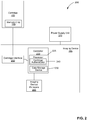
- FIG. 2 illustrates a schematic representation of a cartridge authentication system 200 in accordance with the teachings of this disclosure.
- the cartridge authentication system 200 has an imaging device 205 (e.g., a printer) communicatively coupled with the cartridge 100 described above in connection with FIG. 1 .
- the imaging device 205 of the illustrated example includes a controller 220, which has a processor 225, a data storage device 230 and a cartridge authenticator 240, which may be implemented by the processor 225.
- the imaging device 205 also includes imaging device firmware 245, which may be stored on the data storage device 230, and a cartridge interface 250.
- the firmware 245 of the illustrated example is executed by the processor 225 and causes and/or initiates the processor 225 to access the memory chip 150 of the cartridge 100.
- a power supply unit 275 coupled to the imaging device 205 provides power for both the imaging device 205 and the cartridge 100.
- the example cartridge 100 is installed in a carriage cradle of the example imaging device 205.
- the imaging device 205 of the illustrated example is communicatively coupled to the cartridge 100 to authenticate the cartridge 100 and/or control the cartridge 100 via the cartridge interface 250.
- the cartridge interface 250 of the illustrated example consists of electrical contacts of the imaging device 205 in contact with the conductive pads 140 shown above in connection with FIG. 1 when the cartridge 100 is installed in the cradle of the imaging device 205 to enable the imaging device 205 to communicate with the cartridge 100, control the electrical or ink deposition functions of the cartridge 100, and/or verify the authenticity of the cartridge 100.
- the imaging device 205 accesses a memory address of the memory chip 150 via the cartridge interface 250 to receive an authentication bit sequence (e.g., an array, a bit array, etc.) from the memory chip 150, for example.
- the authentication bit sequence may be a 256-bit sequence or any other appropriate size (16-bit, 1024-bit, etc.).
- the authentication bit sequence may be a multi-dimensional array. In some examples, the entire authentication bit sequence is read in a single step.
- the processor 225 based on instructions provided by the imaging device firmware 245, receives the authentication bit sequence from the memory chip 150 via the cartridge interface 250 and forwards the authentication bit sequence to the cartridge authenticator 240, which transforms (e.g., shifts, re-arranges, scrambles, re-assigns, transposes, etc.) the authentication bit sequence to verify the authenticity of the cartridge 100.
- the cartridge authenticator 240 of the illustrated example determines scrambling bits (e.g., the scrambling bit values) by accessing portion(s) of the authentication bit sequence at pre-defined and/or known addresses of the bit sequence.
- the scrambling bits (e.g., values of the scrambling bits) indicate to the cartridge authenticator 240 and/or the processor 225 a number of address locations to shift the bits of the authentication bit sequence.
- an arithmetic operation defined by and/or between the scrambling bits indicates and/or defines how the cartridge authenticator 240 is to transform the authentication bit sequence.
- the cartridge authenticator 240 has pre-defined transform functions initiated by specific scrambling bit values and/or a relationship between the scrambling bit values (e.g., a sum, etc.).
- the scrambling bit values may be compared to a table to select the pre-defined transform function(s) to transform the authentication bit sequence.
- bits of the authentication bit sequence define a number of transformation cycles to transform the authentication bit sequence.
- the cartridge authenticator 240 verifies the transformed bit sequence. This verification may occur by verifying the transformed bit sequence against a known value, a pre-determine criteria, a checksum, mathematical operations, or any other appropriate verification of a number sequence.
- the cartridge authenticator 240 provides a signal to the processor 225 and/or the cartridge interface 250 to enable use and/communication between the controller 220 and the cartridge 100 via the cartridge interface 250.
- the controller 220 sends an authorization signal to the cartridge 100 to enable use of the cartridge 100 with the imaging device 205.
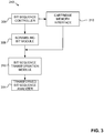
- FIG. 3 illustrates a schematic representation of one example implementation of the example cartridge authenticator 240 of the imaging device 205 of FIG. 2 .
- the cartridge authenticator 240 of the illustrated example includes a bit sequence controller 306, a scrambling bit module 308, a cartridge memory interface 310, a bit sequence transformation module 312, and a transformed bit sequence analyzer 314.
- the bit sequence controller 306 of the illustrated example signals the cartridge memory interface 310 to retrieve an authentication bit sequence from a memory (e.g., a memory, a memory data structure, etc.) of a cartridge (e.g., the cartridge 100) and provide the authentication bit sequence to the bit sequence transformation module 312.
- a memory e.g., a memory, a memory data structure, etc.
- the bit sequence controller 306 triggers the scrambling bit module 308 to provide data, such as memory locations of scrambling bits of the authentication bit sequence and/or the scrambling bits of the authentication bit sequence (e.g., scrambling bit values, converted scrambling bit values, etc.), to the bit sequence transformation module 312 to enable the bit sequence transformation module 312 to transform the authentication bit sequence received from the cartridge memory interface 310 based on the scrambling bits.
- transformation of the authentication bit sequence is further based on static bits of the authentication bit sequence.
- the scrambling bits are excluded from the transformation process.
- the transformed authentication bit sequence is provided to the transformed bit sequence analyzer 314, which verifies the transformed authentication bit sequence.
- the transformed bit sequence analyzer interprets a command based on verifying the transformed bit sequence and/or comparing the received transformed bit sequence to a table of known transformed bit sequences.
- FIG. 4 illustrates an example bit array 400 that is manipulated to a sequence of bit encryption steps.
- the example bit array 400 is subdivided into 4-bit binary sequences.
- the bit array 400 of the illustrated example has static bits (e.g., subsets, portions, sequences, etc.) 402 and 404 at pre-defined (e.g., known) address locations of the example bit array 400.
- the static bits 402 and 404 are distributed randomly throughout the example bit array 400.
- the remaining bits of the example bit sequence are non-static (e.g., movable, writable, etc.).
- the example bit array has non-static bit sequences (e.g., portions) 406, 408, 410, 412, 414 and 416.
- scrambling bits of the example bit array 400 which may be located at pre-defined addresses of the bit array 400, and/or a relationship between the scrambling bits define and/or indicate a transformation method or instructions to transform the example bit array 400.
- the scrambling bits are the static bits 402 and 404 that define a shift of each non-static bit of two memory locations.
- a binary value of a sum of the static bit 402 and the static bit 404 equals a value of two, which is used to define how many address locations to shift each of the non-static bits of the example bit array 400, for example.
- the scrambling bits are equal to the static bits 402 and 404, and are excluded from being shifted and/or moved.
- At least one of the non-static bits comprises the scrambling bits and the scrambling bits may be moved and/or shifted. While a sum of the scrambling bits of the illustrated are used in this example, more complex operations (e.g., multi-step arithmetic operations, varying operations between different memory locations and/or addresses, etc.) between the static bits and/or between the static and non-static bits may be used to define a transformation pattern.
- more complex operations e.g., multi-step arithmetic operations, varying operations between different memory locations and/or addresses, etc.
- the bit sequence (e.g., portion) 406 of the example bit array 400 is about to be shifted two address locations as directed by the sum of the static bits 402 and 404 and indicated by an arrow 418. However, because the static bits 404 are a designated static location, the bit sequence 406 does not overwrite the static bits 404. Instead, the bit sequence 406 is shifted an additional two addresses as indicated by an arrow 420. Because the bit sequence 408 does not have static bits two memory addresses away from of the bit sequence 408, the bit sequence 408 is moved as indicated by an arrow 422. Similarly, the bit sequence 410 is moved two address locations as indicated by an arrow 424, and the bit sequence 412 is also moved as indicated by an arrow 426. In this example, the bit sequences 414 and 416 are moved to later portions of the example bit array 400 (e.g., two memory addresses as defined by the static bits 402 and 404).
- bit sequences e.g., portions
- arrows 428 and 430 indicate bit sequences from later portions (e.g., near or at an end of the bit array 400), which are represented by "XXXX,” of the authentication bit sequence moved (e.g., recursively moved) to memory addresses after the static bits 402.
- the static bits 402, 404 are used to convey information to an imaging device and/or used for manufacturing or operational processes (e.g., signifying manufacturing codes such as lot codes, serial number, etc.). While the example of FIG. 4 illustrates shifts in one direction, the shifts may occur in an opposite direction or some bits may be shifted in different directions from other bits, for example. In some examples, different bits are shifted by different amount of address locations, which may be defined by the scrambling bits, static bits and/or static bit locations. While the examples described above are related to a one-dimensional (1-D) array, the examples disclosed herein may be applied to multidimensional arrays. Additionally, or alternatively, the scrambling bits may define shifting in more than one direction and/or dimension for multidimensional arrays. In some examples, the transformation and/or re-sequencing of the bits is performed in a single step, which may be performed by a multi-threaded processor, for example.
- FIGS. 5 and 6 While an example manner of implementing the cartridge authentication system 200 of FIG. 2 is illustrated in FIGS. 5 and 6 , one or more of the elements, processes and/or devices illustrated in FIGS. 5 and 6 may be combined, divided, re-arranged, omitted, eliminated and/or implemented in any other way.
- FPLD field programmable logic device
- At least one of the example imaging device 205, the example controller 220, the example processor 225, the example data storage device 230, the example cartridge authenticator 240, the example imaging device firmware 245, the example cartridge interface 250, the example cartridge 100, the example memory chip 150, the example bit sequence controller 306, the example scrambling bit module 308, the example cartridge memory interface 310, the example bit sequence transformation module 312 and/or the example transformed bit sequence analyzer 314 is/are hereby expressly defined to include a tangible computer readable storage device or storage disk such as a memory, a digital versatile disk (DVD), a compact disk (CD), a Blu-ray disk, etc.
- DVD digital versatile disk
- CD compact disk
- Blu-ray disk etc.
- example cartridge authentication system 200 of FIG. 2 may include one or more elements, processes and/or devices in addition to, or instead of, those illustrated in FIGS. 5 and 6 , and/or may include more than one of any or all of the illustrated elements, processes and devices.
- the machine readable instructions comprise a program for execution by a processor such as the processor 712 shown in the example processor platform 700 discussed below in connection with FIG. 7 .
- the program may be embodied in software stored on a tangible computer readable storage medium such as a CD-ROM, a floppy disk, a hard drive, a digital versatile disk (DVD), a Blu-ray disk, or a memory associated with the processor 712, but the entire program and/or parts thereof could alternatively be executed by a device other than the processor 712 and/or embodied in firmware or dedicated hardware.
- example program is described with reference to the flowcharts illustrated in FIGS. 5 and 6 , many other methods of implementing the example cartridge authentication system 200 may alternatively be used. For example, the order of execution of the blocks may be changed, and/or some of the blocks described may be changed, eliminated, or combined.
- FIGS. 5 and 6 may be implemented using coded instructions (e.g., computer and/or machine readable instructions) stored on a tangible computer readable storage medium such as a hard disk drive, a flash memory, a read-only memory (ROM), a compact disk (CD), a digital versatile disk (DVD), a cache, a random-access memory (RAM) and/or any other storage device or storage disk in which information is stored for any duration (e.g., for extended time periods, permanently, for brief instances, for temporarily buffering, and/or for caching of the information).
- a tangible computer readable storage medium is expressly defined to include any type of computer readable storage device and/or storage disk and to exclude propagating signals and to exclude transmission media.
- tangible computer readable storage medium and “tangible machine readable storage medium” are used interchangeably. Additionally or alternatively, the example processes of FIGS. 5 and 6 may be implemented using coded instructions (e.g., computer and/or machine readable instructions) stored on a non-transitory computer and/or machine readable medium such as a hard disk drive, a flash memory, a read-only memory, a compact disk, a digital versatile disk, a cache, a random-access memory and/or any other storage device or storage disk in which information is stored for any duration (e.g., for extended time periods, permanently, for brief instances, for temporarily buffering, and/or for caching of the information).
- coded instructions e.g., computer and/or machine readable instructions
- a non-transitory computer and/or machine readable medium such as a hard disk drive, a flash memory, a read-only memory, a compact disk, a digital versatile disk, a cache, a random-access memory and/or any other storage device or storage disk in
- non-transitory computer readable medium is expressly defined to include any type of computer readable storage device and/or storage disk and to exclude propagating signals and to exclude transmission media.
- phrase "at least" is used as the transition term in a preamble of a claim, it is open-ended in the same manner as the term “comprising" is open ended.
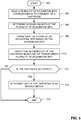
- FIG. 5 is a flowchart representative of example machine readable instructions that may be executed to implement the example cartridge authentication system of FIG. 2 .
- the program of FIG. 5 begins at block 500 where a cartridge (e.g., the cartridge 100) with an authentication memory (e.g., the memory chip 150) has been inserted into an imaging device (e.g., the imaging device 205) (block 500).
- insertion of the cartridge triggers an interface (e.g., the cartridge memory interface 310 of the cartridge authenticator 240) of a controller (e.g., the controller 220) of the imaging device to read and/or receive an authentication bit sequence of the authentication memory of the cartridge (block 502).
- a controller e.g., the controller 220
- the controller of the imaging device determines scrambling bits (e.g., determines values of the scrambling bits) of the authentication bit sequence by accessing known address locations of the authentication bit sequence (block 506).
- the scrambling bit address locations are defined by a scrambling bit module such as the scrambling bit module 308 described above in connection with FIG. 3 .
- a bit sequence transformation module e.g., the bit sequence transformation module of the cartridge authenticator transforms (e.g., rearranges, shifts, transposes, etc.) the authentication bit sequence based on the scrambling bits, mathematical operations of the scrambling bits, and/or mathematical operations between the scrambling bits and the authentication bit sequence, and or any other appropriate transformation and/or scrambling algorithm (block 508).
- the scrambling bits are excluded from this transformation process.
- the scrambling bits define or indicate how many address locations to shift each bit and/or a direction along the bit sequence in which one or more bits are to be moved.
- the transformation of the authentication bit sequence may occur through multiple cycles of moving and/or reassigning bits (e.g., a recursive process that is repeated multiple times).
- the scrambling bits, values of the scrambling bits and/or values resulting from mathematic operations of the scrambling bits are compared to a table to determine a transformation algorithm to be applied to the authentication bit sequence.
- the transformation is further based on static bits of the authentication bit sequence.
- the transformed authentication bit sequence is then verified to determine whether the cartridge is authentic, for example (block 510). As mentioned above, this verification may occur through the transformed bit sequence being an expected value, checksums, and/or any other appropriate verification process. If the cartridge is determined to be authentic (block 512), the cartridge is authorized for use with the imaging device (block 514), and the process ends (516). However, if the cartridge is determined not to be authentic (block 512), the process ends (block 516) until the cartridge is re-inserted or another cartridge is inserted into the imaging device.
- FIG. 5 While the example of FIG. 5 is described in relation to verifying the cartridge, the example process and/or portions of the example process may also be used to encrypt the cartridge (e.g., to write the transformed authentication bit sequence to the memory of the cartridge). Alternatively, portions of the process of FIG. 5 may be reversed and/or re-ordered for other purposes.
- FIG. 6 is another flowchart representative of example machine readable instructions that may be executed to implement the example cartridge 100 of the cartridge authentication system 200 of FIG. 2 .
- a cartridge is being programmed and/or encoded with an authentication bit sequence to prevent third-parties from reverse-engineering the cartridge and to allow the cartridge to be later verified by an imaging device.
- the program of FIG. 6 begins at block 600 where the cartridge (e.g., the cartridge 100) is being prepared to be programmed, encoded and/or receive the authentication bit sequence in a memory (e.g., the memory chip 150), for example (block 600).
- scrambling bits of the authentication bit sequence are determined and/or defined (block 602). In particular, addresses of the scrambling bits of the illustrated example are known.
- the authentication bit sequence and/or the scrambling bits are defined and/or provided by a programming computer and/or device.
- the authentication bit sequence is transformed based on the determined and/or defined scrambling bits (block 604).
- the transformation is further based on static bits of the authentication bit sequence.
- the static bits are excluded from the transformation process.
- the scrambling bits are in static bit locations.
- the scrambling bits are excluded from the transformation process and are used by the imaging device for verification of the cartridge via another transformation process (e.g., a later transformation performed to verify the cartridge) of the authentication bit sequence and/or a copy of the authentication bit sequence used to verify the cartridge.
- the transformed bit sequence of the illustrated example is then written (e.g., encoded) to the memory of the cartridge (block 606).
- a programming device writes the transformed bit sequence to a ROM or EPROM of the cartridge. After the memory of the cartridge is programmed via the programming device, for example, the process ends (block 608).
- FIG. 7 is a block diagram of an example processor platform 700 capable of executing the instructions of FIGS. 5 and 6 to implement the example cartridge authentication system 200 of FIG. 2 .
- the processor platform 700 can be, for example, a server, a personal computer (PC), a cartridge programmer, a printer, an imaging device, a mobile device (e.g., a cell phone, a smart phone, a tablet such as an iPadTM), a personal digital assistant (PDA), an Internet appliance a digital video recorder, a gaming console, a personal video recorder, a set top box, or any other type of computing device.
- PC personal computer
- PDA personal digital assistant
- the processor platform 700 of the illustrated example includes a processor 712.
- the processor 712 of the illustrated example is hardware.
- the processor 712 can be implemented by one or more integrated circuits, logic circuits, microprocessors or controllers from any desired family or manufacturer.
- the processor 712 of the illustrated example includes a local memory 713 (e.g., a cache).
- the processor 712 includes the example controller 220, the example cartridge authenticator 240, the example cartridge interface 250, the example bit sequence controller 306, the scrambling bit module 308, the example cartridge memory interface 310, the example bit sequence transformation module 312, and the example transformed bit sequence analyzer 314.
- the processor 712 of the illustrated example is in communication with a main memory including a volatile memory 714 and a non-volatile memory 716 via a bus 718.
- the volatile memory 714 may be implemented by Synchronous Dynamic Random Access Memory (SDRAM), Dynamic Random Access Memory (DRAM), RAMBUS Dynamic Random Access Memory (RDRAM) and/or any other type of random access memory device.
- the non-volatile memory 716 may be implemented by flash memory and/or any other desired type of memory device. Access to the main memory 714, 716 is controlled by a memory controller.
- the processor platform 700 of the illustrated example also includes an interface circuit 720.
- the interface circuit 720 may be implemented by any type of interface standard, such as an Ethernet interface, a universal serial bus (USB), and/or a PCI express interface.
- one or more input devices 722 are connected to the interface circuit 720.
- the input device(s) 722 permit(s) a user to enter data and commands into the processor 712.
- the input device(s) can be implemented by, for example, an audio sensor, a microphone, a camera (still or video), a keyboard, a button, a mouse, a touchscreen, a track-pad, a trackball, isopoint and/or a voice recognition system.
- One or more output devices 724 are also connected to the interface circuit 720 of the illustrated example.
- the output devices 724 can be implemented, for example, by display devices (e.g., a light emitting diode (LED), an organic light emitting diode (OLED), a liquid crystal display, a cathode ray tube display (CRT), a touchscreen, a tactile output device, a printer and/or speakers).
- the interface circuit 720 of the illustrated example thus, typically includes a graphics driver card, a graphics driver chip or a graphics driver processor.
- the interface circuit 720 of the illustrated example also includes a communication device such as a transmitter, a receiver, a transceiver, a modem and/or network interface card to facilitate exchange of data with external machines (e.g., computing devices of any kind) via a network 726 (e.g., an Ethernet connection, a digital subscriber line (DSL), a telephone line, coaxial cable, a cellular telephone system, etc.).
- a communication device such as a transmitter, a receiver, a transceiver, a modem and/or network interface card to facilitate exchange of data with external machines (e.g., computing devices of any kind) via a network 726 (e.g., an Ethernet connection, a digital subscriber line (DSL), a telephone line, coaxial cable, a cellular telephone system, etc.).
- DSL digital subscriber line
- the processor platform 700 of the illustrated example also includes one or more mass storage devices 728 for storing software and/or data.
- mass storage devices 728 include floppy disk drives, hard drive disks, compact disk drives, Blu-ray disk drives, RAID systems, and digital versatile disk (DVD) drives.
- the coded instructions 732 of FIGS. 5 and 6 may be stored in the mass storage device 728, in the volatile memory 714, in the non-volatile memory 716, and/or on a removable tangible computer readable storage medium such as a CD or DVD.
- the above disclosed methods, apparatus and articles of manufacture provide encryption techniques to encrypt a cartridge and/or interpret an authentication memory of a cartridge to authenticate the cartridge for verification with an imaging device.
- the examples disclosed herein may also reduce and/or eliminate a need for transmission and/or update of encryption keys by defining scrambling bits from a portion of an authentication memory.
Landscapes
- Storage Device Security (AREA)
- Signal Processing For Digital Recording And Reproducing (AREA)
- Studio Devices (AREA)
- Ink Jet (AREA)
- Read Only Memory (AREA)
Claims (17)
- Apparat zur Verwendung mit einer Bildgebungsvorrichtung, wobei die Vorrichtung Folgendes umfasst:einen Speicher (150) für eine Fluidkartusche mit mehreren sequentiellen Bits, einschließlich Verwürfelungsbits, dadurch gekennzeichnet, dass die mehreren sequentiellen Bits in den Speicher geschrieben werden, nachdem die mehreren sequentiellen Bits auf der Grundlage der Verwürfelungsbits der mehreren sequentiellen Bits rekursiv transformiert werden; undeine Speicherschnittstelle (310) für die Fluidkartusche, um es der Bildgebungsvorrichtung zu ermöglichen, auf den Speicher (150) zuzugreifen, um die Fluidkartusche durch Verifizieren der mehreren sequentiellen Bits unter Einsatz der Verwürfelungsbits zu authentifizieren.
- Apparat nach Anspruch 1, wobei die mehreren sequentiellen Bits ferner statische Bits umfassen, die von dem Transformieren ausgeschlossen sind.
- Apparat nach Anspruch 2, wobei die statischen Bits die Verwürfelungsbits umfassen.
- Apparat nach Anspruch 2 oder Anspruch 3, wobei die mehreren sequentiellen Bits ferner auf der Grundlage der statischen Bits transformiert werden.
- Apparat nach einem der Ansprüche 1 bis 4, wobei der Speicher (150) eine EPROM-Speichervorrichtung umfasst.
- Apparat nach einem der Ansprüche 1 bis 5, wobei der Speicher (150) mit einer Druckkopfschaltungsanordnung einer Fluidkartusche einstückig ausgebildet ist.
- Apparat nach einem der Ansprüche 1 bis 6, wobei die Speicherschnittstelle elektrische Kontakte (140) für die Fluidkartusche umfasst, um den Zugriff auf die Speichervorrichtung (150) zu ermöglichen, um die Fluidkartusche zu authentifizieren; und wobei der Apparat ferner eine Druckkopfschaltungsanordnung umfasst, die elektrisch mit der Speichervorrichtung (150) und den elektrischen Kontakten (140) gekoppelt ist.
- Apparat nach Anspruch 7, wobei die Speichervorrichtung (150) mit der Druckkopfschaltungsanordnung einstückig ausgebildet ist.
- Apparat nach einem der Ansprüche 7 oder 8, wobei die Druckkopfschaltungsanordnung eine Druckkopfprägeplatte umfasst.
- Apparat nach einem der Ansprüche 7 bis 9, wobei die Speichervorrichtung (150) eine EPROM-Speichervorrichtung umfasst.
- Fluidkartusche (100), die Folgendes umfasst: ein Fluidreservoir (110) zum Aufnehmen eines Fluids; und einen Apparat nach einem der Ansprüche 7 bis 10.
- Bildgebungsvorrichtung (205) zur Verwendung mit einer Fluidkartusche nach Anspruch 11, die Folgendes umfasst:eine Kartuschenschnittstelle (250), die einen oder mehrere elektrische Kontakte umfasst, die dazu angeordnet sind, den einen oder die mehreren elektrischen Kontakte der Fluidkartusche zu berühren;einen Prozessor (225), der dazu angeordnet ist, über die Kartuschenschnittstelle (250) mehrere sequentielle Bits zu empfangen, die auf einem Speicherchip der Fluidkartusche gespeichert sind; undeinen Kartuschenauthentifizierer (240), der dazu angeordnet ist, die mehreren sequentiellen Bits zu transformieren, um die Authentizität der Fluidkartusche zu verifizieren.
- Verfahren (500) zum Authentifizieren einer Fluidkartusche nach Anspruch 11, das Folgendes umfasst:Empfangen (502) einer Authentifizierungsbitsequenz, die in einem Speicherchip der Fluidkartusche gespeichert ist;Bestimmen (506) eines oder mehrerer Verwürfelungsbits der Authentifizierungsbitsequenz;Transformieren (508) der Authentifizierungsbitsequenz basierend auf dem einen oder den mehreren Verwürfelungsbits;Verifizieren (510) der transformierten Authentifizierungsbitsequenz, um zu bestimmen, ob die Fluidkartusche authentisch ist; undAutorisieren (514) der Fluidkartusche, wenn die transformierte Authentifizierungsbitsequenz verifizierbar ist.
- Apparat für eine Fluidkartusche, wobei der Apparat Folgendes umfasst:
eine Speicherdatenstruktur (150) für einen Fluidkartuschenspeicher, die mehrere sequentielle Authentifizierungsbits einschließlich Verwürfelungsbits umfasst, dadurch gekennzeichnet, dass die mehreren sequentiellen Bits auf der Grundlage von Verwürfelungsbits rekursiv transformiert worden sind, bevor die mehreren sequentiellen Bits in die Speicherdatenstruktur (150) geschrieben werden; wobei die sequentiellen Bits von einer Bilderzeugungsvorrichtung verwendet werden können, um die Fluidkartusche durch Verifizieren der mehreren sequentiellen Bits unter Einsatz der Verwürfelungsbits zu authentifizieren. - Apparat nach Anspruch 14, wobei die mehreren sequentiellen Bits statische Bits umfassen, die von dem Transformieren ausgeschlossen sind.
- Apparat nach Anspruch 15, wobei sich die statischen Bits an definierten Adressstellen des Speichers (150) befinden.
- Apparat nach Anspruch 15, wobei die mehreren sequentiellen Bits ferner auf der Grundlage der statischen Bits transformiert werden.
Applications Claiming Priority (1)
| Application Number | Priority Date | Filing Date | Title |
|---|---|---|---|
| PCT/US2014/063381 WO2016068990A1 (en) | 2014-10-31 | 2014-10-31 | Encryption of fluid cartridges for use with imaging devices |
Publications (3)
| Publication Number | Publication Date |
|---|---|
| EP3201003A1 EP3201003A1 (de) | 2017-08-09 |
| EP3201003A4 EP3201003A4 (de) | 2018-05-30 |
| EP3201003B1 true EP3201003B1 (de) | 2019-12-04 |
Family
ID=55858091
Family Applications (1)
| Application Number | Title | Priority Date | Filing Date |
|---|---|---|---|
| EP14904953.8A Active EP3201003B1 (de) | 2014-10-31 | 2014-10-31 | Verschlüsselung von flüssigkeitskartuschen zur verwendung in bildgebungsvorrichtungen |
Country Status (11)
| Country | Link |
|---|---|
| US (1) | US9815289B2 (de) |
| EP (1) | EP3201003B1 (de) |
| KR (1) | KR101993540B1 (de) |
| CN (1) | CN107073947B (de) |
| AU (1) | AU2014410129B2 (de) |
| BR (1) | BR112017008679B1 (de) |
| CA (1) | CA2965856C (de) |
| ES (1) | ES2767052T3 (de) |
| RU (1) | RU2673620C2 (de) |
| TW (1) | TWI655102B (de) |
| WO (1) | WO2016068990A1 (de) |
Families Citing this family (16)
| Publication number | Priority date | Publication date | Assignee | Title |
|---|---|---|---|---|
| RU2673620C2 (ru) | 2014-10-31 | 2018-11-28 | Хьюлетт-Паккард Дивелопмент Компани, Л.П. | Шифрование картриджей с текучей средой для использования в устройствах формирования изображения |
| US9922474B1 (en) * | 2017-02-14 | 2018-03-20 | Multipure International | Systems and methods for authenticating a cartridge |
| CN108116053B (zh) * | 2017-12-19 | 2019-07-26 | 杭州旗捷科技有限公司 | 一种耗材芯片认证方法、耗材芯片及成像盒 |
| CN109951429A (zh) * | 2017-12-21 | 2019-06-28 | 珠海纳思达企业管理有限公司 | 打印机墨盒验证方法、系统及打印机 |
| JP7036582B2 (ja) * | 2017-12-22 | 2022-03-15 | 株式会社東芝 | 画像形成装置及び制御方法 |
| FR3076925B1 (fr) * | 2018-01-16 | 2020-01-24 | Proton World International N.V. | Fonction cryptographique |
| EP3776357B1 (de) * | 2018-04-13 | 2024-05-22 | Lexmark International, Inc. | Chip und versorgungselement für bildgebungsvorrichtung, einschliesslich kommunikation |
| EP3765913A1 (de) | 2018-08-30 | 2021-01-20 | Hewlett-Packard Development Company, L.P. | Kontakte für eine druckpartikeleingabeaussparung |
| JP7400202B2 (ja) * | 2019-03-28 | 2023-12-19 | ブラザー工業株式会社 | 画像記録装置 |
| WO2021054981A1 (en) | 2019-09-20 | 2021-03-25 | Hewlett-Packard Development Company, L.P. | Supply and mixing cartridges |
| US11590763B2 (en) | 2019-09-20 | 2023-02-28 | Hewlett-Packard Development Company, L.P. | Printer recirculation control |
| CN110920262B (zh) * | 2019-12-13 | 2021-03-23 | 珠海艾派克微电子有限公司 | 一种耗材芯片及耗材合法性校验方法 |
| CN112571970B (zh) * | 2020-12-08 | 2021-12-14 | 珠海奔图电子有限公司 | 图像形成控制方法、耗材芯片及图像形成装置、耗材 |
| EP4012504B1 (de) | 2020-12-08 | 2023-07-12 | Zhuhai Pantum Electronics Co., Ltd. | Verfahren zur bilderzeugungssteuerung, verbrauchbarer chip, bilderzeugungsgerät und verbrauchsmaterial |
| US20220382850A1 (en) * | 2021-05-26 | 2022-12-01 | Lexmark International, Inc. | Authentication using analog signal challenge |
| WO2025042383A1 (en) * | 2023-08-18 | 2025-02-27 | Hewlett-Packard Development Company, L.P. | Cartridge with multiple containers for an image recording apparatus |
Family Cites Families (14)
| Publication number | Priority date | Publication date | Assignee | Title |
|---|---|---|---|---|
| US6618117B2 (en) * | 1997-07-12 | 2003-09-09 | Silverbrook Research Pty Ltd | Image sensing apparatus including a microcontroller |
| US6547364B2 (en) * | 1997-07-12 | 2003-04-15 | Silverbrook Research Pty Ltd | Printing cartridge with an integrated circuit device |
| JP2002207807A (ja) * | 2000-09-19 | 2002-07-26 | Seiko Epson Corp | 機器の別売り部品、別売り部品を有する機器、アクセス装置、別売り部品の流通方法、および、インクカートリッジ |
| US6616260B2 (en) * | 2001-05-25 | 2003-09-09 | Hewlett-Packard Development Company, L.P. | Robust bit scheme for a memory of a replaceable printer component |
| US6820972B2 (en) * | 2002-03-29 | 2004-11-23 | Hewlett-Packard Development Company, L.P. | Printing cartridge pigment replenishment apparatus and method |
| BRPI0609896A2 (pt) * | 2005-05-30 | 2010-05-11 | Seiko Epson Corp | dispositivo de memória de semicondutor |
| JP4764735B2 (ja) * | 2006-02-03 | 2011-09-07 | 株式会社リコー | 画像形成装置、画像処理プログラム及び画像処理プログラムを格納する記憶媒体 |
| US8752165B2 (en) * | 2008-05-29 | 2014-06-10 | Apple Inc. | Provisioning secrets in an unsecured environment |
| JP5035128B2 (ja) * | 2008-06-13 | 2012-09-26 | コニカミノルタビジネステクノロジーズ株式会社 | 画像形成装置、及びプロセスカートリッジ認証システム |
| WO2013048430A1 (en) * | 2011-09-30 | 2013-04-04 | Hewlett-Packard Development Company, L.P. | Authentication systems and methods |
| WO2013062528A1 (en) * | 2011-10-25 | 2013-05-02 | Hewlett-Packard Development Company, L.P. | Verification record for a replaceable supply |
| US9461816B2 (en) * | 2012-12-26 | 2016-10-04 | Intel Corporation | Methods, systems and apparatus to reduce processor demands during encryption |
| JP6176982B2 (ja) * | 2013-04-11 | 2017-08-09 | キヤノン株式会社 | 印刷装置及びその制御方法 |
| RU2673620C2 (ru) | 2014-10-31 | 2018-11-28 | Хьюлетт-Паккард Дивелопмент Компани, Л.П. | Шифрование картриджей с текучей средой для использования в устройствах формирования изображения |
-
2014
- 2014-10-31 RU RU2017114375A patent/RU2673620C2/ru active
- 2014-10-31 WO PCT/US2014/063381 patent/WO2016068990A1/en not_active Ceased
- 2014-10-31 ES ES14904953T patent/ES2767052T3/es active Active
- 2014-10-31 KR KR1020177011609A patent/KR101993540B1/ko not_active Expired - Fee Related
- 2014-10-31 CA CA2965856A patent/CA2965856C/en active Active
- 2014-10-31 BR BR112017008679-4A patent/BR112017008679B1/pt not_active IP Right Cessation
- 2014-10-31 AU AU2014410129A patent/AU2014410129B2/en active Active
- 2014-10-31 EP EP14904953.8A patent/EP3201003B1/de active Active
- 2014-10-31 CN CN201480083026.5A patent/CN107073947B/zh active Active
-
2015
- 2015-10-14 TW TW104133721A patent/TWI655102B/zh not_active IP Right Cessation
-
2017
- 2017-04-26 US US15/498,224 patent/US9815289B2/en active Active
Non-Patent Citations (1)
| Title |
|---|
| None * |
Also Published As
| Publication number | Publication date |
|---|---|
| CN107073947A (zh) | 2017-08-18 |
| KR101993540B1 (ko) | 2019-06-26 |
| BR112017008679B1 (pt) | 2021-12-07 |
| CA2965856C (en) | 2020-08-18 |
| CN107073947B (zh) | 2019-07-30 |
| BR112017008679A2 (pt) | 2018-08-28 |
| US20170225476A1 (en) | 2017-08-10 |
| US9815289B2 (en) | 2017-11-14 |
| WO2016068990A1 (en) | 2016-05-06 |
| EP3201003A1 (de) | 2017-08-09 |
| KR20170061158A (ko) | 2017-06-02 |
| TWI655102B (zh) | 2019-04-01 |
| CA2965856A1 (en) | 2016-05-06 |
| AU2014410129B2 (en) | 2018-03-08 |
| ES2767052T3 (es) | 2020-06-16 |
| TW201632364A (zh) | 2016-09-16 |
| AU2014410129A1 (en) | 2017-05-18 |
| RU2017114375A3 (de) | 2018-10-25 |
| RU2017114375A (ru) | 2018-10-25 |
| EP3201003A4 (de) | 2018-05-30 |
| RU2673620C2 (ru) | 2018-11-28 |
Similar Documents
| Publication | Publication Date | Title |
|---|---|---|
| EP3201003B1 (de) | Verschlüsselung von flüssigkeitskartuschen zur verwendung in bildgebungsvorrichtungen | |
| US9489508B2 (en) | Device functionality access control using unique device credentials | |
| JP6072091B2 (ja) | アプリケーション・プログラム用の安全なアクセス方法および安全なアクセス装置 | |
| US7984303B1 (en) | Flash memory devices with security features | |
| CN101968834A (zh) | 电子产品的防抄板加密方法和装置 | |
| CN112612486B (zh) | 存储器烧录方法、装置和待烧录芯片 | |
| CN105528560A (zh) | 基于物理不可克隆功能的安全数据存储 | |
| US10444792B2 (en) | Unlocking control system, method and wearable device using the same | |
| US11157181B2 (en) | Card activation device and methods for authenticating and activating a data storage device by using a card activation device | |
| CN115277143B (zh) | 一种数据安全传输方法、装置、设备及存储介质 | |
| US20190370501A1 (en) | Storage device and verification thereof | |
| US8880900B2 (en) | Memory system | |
| HK1236168B (en) | Encryption of fluid cartridges for use with imaging devices | |
| HK1236168A1 (en) | Encryption of fluid cartridges for use with imaging devices | |
| US20190369902A1 (en) | Storage device and verification thereof | |
| US11101994B2 (en) | Method of provisioning key information and apparatus using the method | |
| US10606520B2 (en) | Methods and apparatus to read from a nonvolatile memory device | |
| CN101311939A (zh) | 操作系统的自引导、安全访问控制存储技术实现方法 | |
| US20130117574A1 (en) | Memory device and system with secure key memory and access logic | |
| KR101776845B1 (ko) | 키 조작에 대한 보호 | |
| JP3230803U (ja) | 暗号化usb保存装置 | |
| CN121456890A (zh) | 安全存储系统及使用方法 | |
| JP2013026870A (ja) | 情報記録媒体と認証管理方法および認証管理システム | |
| KR20140060919A (ko) | 메모리 장치를 이용하는 방법 및 그 장치 | |
| HK1062215A1 (en) | Portable biodata protected data storage unit |
Legal Events
| Date | Code | Title | Description |
|---|---|---|---|
| STAA | Information on the status of an ep patent application or granted ep patent |
Free format text: STATUS: THE INTERNATIONAL PUBLICATION HAS BEEN MADE |
|
| PUAI | Public reference made under article 153(3) epc to a published international application that has entered the european phase |
Free format text: ORIGINAL CODE: 0009012 |
|
| STAA | Information on the status of an ep patent application or granted ep patent |
Free format text: STATUS: REQUEST FOR EXAMINATION WAS MADE |
|
| 17P | Request for examination filed |
Effective date: 20170503 |
|
| AK | Designated contracting states |
Kind code of ref document: A1 Designated state(s): AL AT BE BG CH CY CZ DE DK EE ES FI FR GB GR HR HU IE IS IT LI LT LU LV MC MK MT NL NO PL PT RO RS SE SI SK SM TR |
|
| AX | Request for extension of the european patent |
Extension state: BA ME |
|
| DAX | Request for extension of the european patent (deleted) | ||
| REG | Reference to a national code |
Ref country code: HK Ref legal event code: DE Ref document number: 1236168 Country of ref document: HK |
|
| STAA | Information on the status of an ep patent application or granted ep patent |
Free format text: STATUS: EXAMINATION IS IN PROGRESS |
|
| A4 | Supplementary search report drawn up and despatched |
Effective date: 20180502 |
|
| RIC1 | Information provided on ipc code assigned before grant |
Ipc: B41J 29/393 20060101ALI20180424BHEP Ipc: B41J 2/175 20060101AFI20180424BHEP Ipc: B41J 2/135 20060101ALI20180424BHEP |
|
| 17Q | First examination report despatched |
Effective date: 20180522 |
|
| RAP1 | Party data changed (applicant data changed or rights of an application transferred) |
Owner name: HEWLETT-PACKARD DEVELOPMENT COMPANY, L.P. |
|
| GRAP | Despatch of communication of intention to grant a patent |
Free format text: ORIGINAL CODE: EPIDOSNIGR1 |
|
| STAA | Information on the status of an ep patent application or granted ep patent |
Free format text: STATUS: GRANT OF PATENT IS INTENDED |
|
| INTG | Intention to grant announced |
Effective date: 20190814 |
|
| GRAS | Grant fee paid |
Free format text: ORIGINAL CODE: EPIDOSNIGR3 |
|
| GRAA | (expected) grant |
Free format text: ORIGINAL CODE: 0009210 |
|
| STAA | Information on the status of an ep patent application or granted ep patent |
Free format text: STATUS: THE PATENT HAS BEEN GRANTED |
|
| AK | Designated contracting states |
Kind code of ref document: B1 Designated state(s): AL AT BE BG CH CY CZ DE DK EE ES FI FR GB GR HR HU IE IS IT LI LT LU LV MC MK MT NL NO PL PT RO RS SE SI SK SM TR |
|
| REG | Reference to a national code |
Ref country code: GB Ref legal event code: FG4D |
|
| REG | Reference to a national code |
Ref country code: CH Ref legal event code: EP |
|
| REG | Reference to a national code |
Ref country code: AT Ref legal event code: REF Ref document number: 1208899 Country of ref document: AT Kind code of ref document: T Effective date: 20191215 |
|
| REG | Reference to a national code |
Ref country code: DE Ref legal event code: R096 Ref document number: 602014058092 Country of ref document: DE |
|
| REG | Reference to a national code |
Ref country code: IE Ref legal event code: FG4D |
|
| REG | Reference to a national code |
Ref country code: NL Ref legal event code: FP |
|
| REG | Reference to a national code |
Ref country code: LT Ref legal event code: MG4D |
|
| PG25 | Lapsed in a contracting state [announced via postgrant information from national office to epo] |
Ref country code: LV Free format text: LAPSE BECAUSE OF FAILURE TO SUBMIT A TRANSLATION OF THE DESCRIPTION OR TO PAY THE FEE WITHIN THE PRESCRIBED TIME-LIMIT Effective date: 20191204 Ref country code: LT Free format text: LAPSE BECAUSE OF FAILURE TO SUBMIT A TRANSLATION OF THE DESCRIPTION OR TO PAY THE FEE WITHIN THE PRESCRIBED TIME-LIMIT Effective date: 20191204 Ref country code: NO Free format text: LAPSE BECAUSE OF FAILURE TO SUBMIT A TRANSLATION OF THE DESCRIPTION OR TO PAY THE FEE WITHIN THE PRESCRIBED TIME-LIMIT Effective date: 20200304 Ref country code: GR Free format text: LAPSE BECAUSE OF FAILURE TO SUBMIT A TRANSLATION OF THE DESCRIPTION OR TO PAY THE FEE WITHIN THE PRESCRIBED TIME-LIMIT Effective date: 20200305 Ref country code: BG Free format text: LAPSE BECAUSE OF FAILURE TO SUBMIT A TRANSLATION OF THE DESCRIPTION OR TO PAY THE FEE WITHIN THE PRESCRIBED TIME-LIMIT Effective date: 20200304 Ref country code: SE Free format text: LAPSE BECAUSE OF FAILURE TO SUBMIT A TRANSLATION OF THE DESCRIPTION OR TO PAY THE FEE WITHIN THE PRESCRIBED TIME-LIMIT Effective date: 20191204 Ref country code: FI Free format text: LAPSE BECAUSE OF FAILURE TO SUBMIT A TRANSLATION OF THE DESCRIPTION OR TO PAY THE FEE WITHIN THE PRESCRIBED TIME-LIMIT Effective date: 20191204 |
|
| PG25 | Lapsed in a contracting state [announced via postgrant information from national office to epo] |
Ref country code: RS Free format text: LAPSE BECAUSE OF FAILURE TO SUBMIT A TRANSLATION OF THE DESCRIPTION OR TO PAY THE FEE WITHIN THE PRESCRIBED TIME-LIMIT Effective date: 20191204 Ref country code: HR Free format text: LAPSE BECAUSE OF FAILURE TO SUBMIT A TRANSLATION OF THE DESCRIPTION OR TO PAY THE FEE WITHIN THE PRESCRIBED TIME-LIMIT Effective date: 20191204 |
|
| REG | Reference to a national code |
Ref country code: ES Ref legal event code: FG2A Ref document number: 2767052 Country of ref document: ES Kind code of ref document: T3 Effective date: 20200616 |
|
| PG25 | Lapsed in a contracting state [announced via postgrant information from national office to epo] |
Ref country code: AL Free format text: LAPSE BECAUSE OF FAILURE TO SUBMIT A TRANSLATION OF THE DESCRIPTION OR TO PAY THE FEE WITHIN THE PRESCRIBED TIME-LIMIT Effective date: 20191204 |
|
| PG25 | Lapsed in a contracting state [announced via postgrant information from national office to epo] |
Ref country code: EE Free format text: LAPSE BECAUSE OF FAILURE TO SUBMIT A TRANSLATION OF THE DESCRIPTION OR TO PAY THE FEE WITHIN THE PRESCRIBED TIME-LIMIT Effective date: 20191204 Ref country code: PT Free format text: LAPSE BECAUSE OF FAILURE TO SUBMIT A TRANSLATION OF THE DESCRIPTION OR TO PAY THE FEE WITHIN THE PRESCRIBED TIME-LIMIT Effective date: 20200429 Ref country code: RO Free format text: LAPSE BECAUSE OF FAILURE TO SUBMIT A TRANSLATION OF THE DESCRIPTION OR TO PAY THE FEE WITHIN THE PRESCRIBED TIME-LIMIT Effective date: 20191204 Ref country code: CZ Free format text: LAPSE BECAUSE OF FAILURE TO SUBMIT A TRANSLATION OF THE DESCRIPTION OR TO PAY THE FEE WITHIN THE PRESCRIBED TIME-LIMIT Effective date: 20191204 |
|
| PG25 | Lapsed in a contracting state [announced via postgrant information from national office to epo] |
Ref country code: SM Free format text: LAPSE BECAUSE OF FAILURE TO SUBMIT A TRANSLATION OF THE DESCRIPTION OR TO PAY THE FEE WITHIN THE PRESCRIBED TIME-LIMIT Effective date: 20191204 Ref country code: IS Free format text: LAPSE BECAUSE OF FAILURE TO SUBMIT A TRANSLATION OF THE DESCRIPTION OR TO PAY THE FEE WITHIN THE PRESCRIBED TIME-LIMIT Effective date: 20200404 Ref country code: SK Free format text: LAPSE BECAUSE OF FAILURE TO SUBMIT A TRANSLATION OF THE DESCRIPTION OR TO PAY THE FEE WITHIN THE PRESCRIBED TIME-LIMIT Effective date: 20191204 |
|
| REG | Reference to a national code |
Ref country code: DE Ref legal event code: R097 Ref document number: 602014058092 Country of ref document: DE |
|
| REG | Reference to a national code |
Ref country code: AT Ref legal event code: MK05 Ref document number: 1208899 Country of ref document: AT Kind code of ref document: T Effective date: 20191204 |
|
| PLBE | No opposition filed within time limit |
Free format text: ORIGINAL CODE: 0009261 |
|
| STAA | Information on the status of an ep patent application or granted ep patent |
Free format text: STATUS: NO OPPOSITION FILED WITHIN TIME LIMIT |
|
| PG25 | Lapsed in a contracting state [announced via postgrant information from national office to epo] |
Ref country code: DK Free format text: LAPSE BECAUSE OF FAILURE TO SUBMIT A TRANSLATION OF THE DESCRIPTION OR TO PAY THE FEE WITHIN THE PRESCRIBED TIME-LIMIT Effective date: 20191204 |
|
| 26N | No opposition filed |
Effective date: 20200907 |
|
| PG25 | Lapsed in a contracting state [announced via postgrant information from national office to epo] |
Ref country code: SI Free format text: LAPSE BECAUSE OF FAILURE TO SUBMIT A TRANSLATION OF THE DESCRIPTION OR TO PAY THE FEE WITHIN THE PRESCRIBED TIME-LIMIT Effective date: 20191204 Ref country code: PL Free format text: LAPSE BECAUSE OF FAILURE TO SUBMIT A TRANSLATION OF THE DESCRIPTION OR TO PAY THE FEE WITHIN THE PRESCRIBED TIME-LIMIT Effective date: 20191204 Ref country code: AT Free format text: LAPSE BECAUSE OF FAILURE TO SUBMIT A TRANSLATION OF THE DESCRIPTION OR TO PAY THE FEE WITHIN THE PRESCRIBED TIME-LIMIT Effective date: 20191204 |
|
| REG | Reference to a national code |
Ref country code: CH Ref legal event code: PL |
|
| PG25 | Lapsed in a contracting state [announced via postgrant information from national office to epo] |
Ref country code: LU Free format text: LAPSE BECAUSE OF NON-PAYMENT OF DUE FEES Effective date: 20201031 Ref country code: MC Free format text: LAPSE BECAUSE OF FAILURE TO SUBMIT A TRANSLATION OF THE DESCRIPTION OR TO PAY THE FEE WITHIN THE PRESCRIBED TIME-LIMIT Effective date: 20191204 |
|
| REG | Reference to a national code |
Ref country code: BE Ref legal event code: MM Effective date: 20201031 |
|
| PG25 | Lapsed in a contracting state [announced via postgrant information from national office to epo] |
Ref country code: LI Free format text: LAPSE BECAUSE OF NON-PAYMENT OF DUE FEES Effective date: 20201031 Ref country code: BE Free format text: LAPSE BECAUSE OF NON-PAYMENT OF DUE FEES Effective date: 20201031 Ref country code: CH Free format text: LAPSE BECAUSE OF NON-PAYMENT OF DUE FEES Effective date: 20201031 |
|
| PG25 | Lapsed in a contracting state [announced via postgrant information from national office to epo] |
Ref country code: IE Free format text: LAPSE BECAUSE OF NON-PAYMENT OF DUE FEES Effective date: 20201031 |
|
| PG25 | Lapsed in a contracting state [announced via postgrant information from national office to epo] |
Ref country code: TR Free format text: LAPSE BECAUSE OF FAILURE TO SUBMIT A TRANSLATION OF THE DESCRIPTION OR TO PAY THE FEE WITHIN THE PRESCRIBED TIME-LIMIT Effective date: 20191204 Ref country code: MT Free format text: LAPSE BECAUSE OF FAILURE TO SUBMIT A TRANSLATION OF THE DESCRIPTION OR TO PAY THE FEE WITHIN THE PRESCRIBED TIME-LIMIT Effective date: 20191204 Ref country code: CY Free format text: LAPSE BECAUSE OF FAILURE TO SUBMIT A TRANSLATION OF THE DESCRIPTION OR TO PAY THE FEE WITHIN THE PRESCRIBED TIME-LIMIT Effective date: 20191204 |
|
| PG25 | Lapsed in a contracting state [announced via postgrant information from national office to epo] |
Ref country code: MK Free format text: LAPSE BECAUSE OF FAILURE TO SUBMIT A TRANSLATION OF THE DESCRIPTION OR TO PAY THE FEE WITHIN THE PRESCRIBED TIME-LIMIT Effective date: 20191204 |
|
| REG | Reference to a national code |
Ref country code: DE Ref legal event code: R082 Ref document number: 602014058092 Country of ref document: DE Representative=s name: NOVAGRAAF BREVETS, FR |
|
| PGFP | Annual fee paid to national office [announced via postgrant information from national office to epo] |
Ref country code: NL Payment date: 20250923 Year of fee payment: 12 Ref country code: IT Payment date: 20250923 Year of fee payment: 12 |
|
| PGFP | Annual fee paid to national office [announced via postgrant information from national office to epo] |
Ref country code: GB Payment date: 20250923 Year of fee payment: 12 |
|
| PGFP | Annual fee paid to national office [announced via postgrant information from national office to epo] |
Ref country code: FR Payment date: 20250924 Year of fee payment: 12 |
|
| PGFP | Annual fee paid to national office [announced via postgrant information from national office to epo] |
Ref country code: DE Payment date: 20250923 Year of fee payment: 12 |
|
| PGFP | Annual fee paid to national office [announced via postgrant information from national office to epo] |
Ref country code: ES Payment date: 20251103 Year of fee payment: 12 |