EP3201942B1 - Messwafer zum messen der strahlungs- und temperaturexposition von wafern entlang einer herstellungsprozesslinie - Google Patents
Messwafer zum messen der strahlungs- und temperaturexposition von wafern entlang einer herstellungsprozesslinie Download PDFInfo
- Publication number
- EP3201942B1 EP3201942B1 EP15851269.9A EP15851269A EP3201942B1 EP 3201942 B1 EP3201942 B1 EP 3201942B1 EP 15851269 A EP15851269 A EP 15851269A EP 3201942 B1 EP3201942 B1 EP 3201942B1
- Authority
- EP
- European Patent Office
- Prior art keywords
- light
- assembly
- wafer
- intensity
- sensors
- Prior art date
- Legal status (The legal status is an assumption and is not a legal conclusion. Google has not performed a legal analysis and makes no representation as to the accuracy of the status listed.)
- Active
Links
Images


Classifications
-
- G—PHYSICS
- G01—MEASURING; TESTING
- G01J—MEASUREMENT OF INTENSITY, VELOCITY, SPECTRAL CONTENT, POLARISATION, PHASE OR PULSE CHARACTERISTICS OF INFRARED, VISIBLE OR ULTRAVIOLET LIGHT; COLORIMETRY; RADIATION PYROMETRY
- G01J1/00—Photometry, e.g. photographic exposure meter
- G01J1/42—Photometry, e.g. photographic exposure meter using electric radiation detectors
- G01J1/429—Photometry, e.g. photographic exposure meter using electric radiation detectors applied to measurement of ultraviolet light
-
- G—PHYSICS
- G01—MEASURING; TESTING
- G01J—MEASUREMENT OF INTENSITY, VELOCITY, SPECTRAL CONTENT, POLARISATION, PHASE OR PULSE CHARACTERISTICS OF INFRARED, VISIBLE OR ULTRAVIOLET LIGHT; COLORIMETRY; RADIATION PYROMETRY
- G01J1/00—Photometry, e.g. photographic exposure meter
- G01J1/02—Details
- G01J1/0204—Compact construction
-
- G—PHYSICS
- G01—MEASURING; TESTING
- G01J—MEASUREMENT OF INTENSITY, VELOCITY, SPECTRAL CONTENT, POLARISATION, PHASE OR PULSE CHARACTERISTICS OF INFRARED, VISIBLE OR ULTRAVIOLET LIGHT; COLORIMETRY; RADIATION PYROMETRY
- G01J1/00—Photometry, e.g. photographic exposure meter
- G01J1/02—Details
- G01J1/0271—Housings; Attachments or accessories for photometers
-
- G—PHYSICS
- G01—MEASURING; TESTING
- G01J—MEASUREMENT OF INTENSITY, VELOCITY, SPECTRAL CONTENT, POLARISATION, PHASE OR PULSE CHARACTERISTICS OF INFRARED, VISIBLE OR ULTRAVIOLET LIGHT; COLORIMETRY; RADIATION PYROMETRY
- G01J1/00—Photometry, e.g. photographic exposure meter
- G01J1/02—Details
- G01J1/04—Optical or mechanical part supplementary adjustable parts
- G01J1/0407—Optical elements not provided otherwise, e.g. manifolds, windows, holograms, gratings
-
- G—PHYSICS
- G01—MEASURING; TESTING
- G01J—MEASUREMENT OF INTENSITY, VELOCITY, SPECTRAL CONTENT, POLARISATION, PHASE OR PULSE CHARACTERISTICS OF INFRARED, VISIBLE OR ULTRAVIOLET LIGHT; COLORIMETRY; RADIATION PYROMETRY
- G01J1/00—Photometry, e.g. photographic exposure meter
- G01J1/58—Photometry, e.g. photographic exposure meter using luminescence generated by light
-
- G—PHYSICS
- G01—MEASURING; TESTING
- G01J—MEASUREMENT OF INTENSITY, VELOCITY, SPECTRAL CONTENT, POLARISATION, PHASE OR PULSE CHARACTERISTICS OF INFRARED, VISIBLE OR ULTRAVIOLET LIGHT; COLORIMETRY; RADIATION PYROMETRY
- G01J5/00—Radiation pyrometry, e.g. infrared or optical thermometry
- G01J5/02—Constructional details
- G01J5/04—Casings
-
- G—PHYSICS
- G01—MEASURING; TESTING
- G01J—MEASUREMENT OF INTENSITY, VELOCITY, SPECTRAL CONTENT, POLARISATION, PHASE OR PULSE CHARACTERISTICS OF INFRARED, VISIBLE OR ULTRAVIOLET LIGHT; COLORIMETRY; RADIATION PYROMETRY
- G01J5/00—Radiation pyrometry, e.g. infrared or optical thermometry
- G01J5/02—Constructional details
- G01J5/08—Optical arrangements
- G01J5/0818—Waveguides
-
- G—PHYSICS
- G01—MEASURING; TESTING
- G01J—MEASUREMENT OF INTENSITY, VELOCITY, SPECTRAL CONTENT, POLARISATION, PHASE OR PULSE CHARACTERISTICS OF INFRARED, VISIBLE OR ULTRAVIOLET LIGHT; COLORIMETRY; RADIATION PYROMETRY
- G01J5/00—Radiation pyrometry, e.g. infrared or optical thermometry
- G01J5/10—Radiation pyrometry, e.g. infrared or optical thermometry using electric radiation detectors
-
- G—PHYSICS
- G01—MEASURING; TESTING
- G01K—MEASURING TEMPERATURE; MEASURING QUANTITY OF HEAT; THERMALLY-SENSITIVE ELEMENTS NOT OTHERWISE PROVIDED FOR
- G01K11/00—Measuring temperature based upon physical or chemical changes not covered by groups G01K3/00, G01K5/00, G01K7/00 or G01K9/00
- G01K11/20—Measuring temperature based upon physical or chemical changes not covered by groups G01K3/00, G01K5/00, G01K7/00 or G01K9/00 using thermoluminescent materials
-
- H—ELECTRICITY
- H10—SEMICONDUCTOR DEVICES; ELECTRIC SOLID-STATE DEVICES NOT OTHERWISE PROVIDED FOR
- H10P—GENERIC PROCESSES OR APPARATUS FOR THE MANUFACTURE OR TREATMENT OF DEVICES COVERED BY CLASS H10
- H10P72/00—Handling or holding of wafers, substrates or devices during manufacture or treatment thereof
- H10P72/06—Apparatus for monitoring, sorting, marking, testing or measuring
- H10P72/0602—Temperature monitoring
-
- H—ELECTRICITY
- H10—SEMICONDUCTOR DEVICES; ELECTRIC SOLID-STATE DEVICES NOT OTHERWISE PROVIDED FOR
- H10P—GENERIC PROCESSES OR APPARATUS FOR THE MANUFACTURE OR TREATMENT OF DEVICES COVERED BY CLASS H10
- H10P72/00—Handling or holding of wafers, substrates or devices during manufacture or treatment thereof
- H10P72/06—Apparatus for monitoring, sorting, marking, testing or measuring
- H10P72/0604—Process monitoring, e.g. flow or thickness monitoring
-
- H—ELECTRICITY
- H10—SEMICONDUCTOR DEVICES; ELECTRIC SOLID-STATE DEVICES NOT OTHERWISE PROVIDED FOR
- H10P—GENERIC PROCESSES OR APPARATUS FOR THE MANUFACTURE OR TREATMENT OF DEVICES COVERED BY CLASS H10
- H10P74/00—Testing or measuring during manufacture or treatment of wafers, substrates or devices
- H10P74/20—Testing or measuring during manufacture or treatment of wafers, substrates or devices characterised by the properties tested or measured, e.g. structural or electrical properties
Definitions
- the present invention generally relates to radiation and temperature monitoring of wafers along a semiconductor process line, and, in particular, to monitoring ultraviolet (UV) light and temperature exposure of wafers in process settings involving UV light exposure.
- UV ultraviolet
- UV radiation uniformity within a processing system e.g., low K thin film curing system
- Current methods are unable to simultaneously monitor both UV radiation intensity and temperature in under the extreme conditions (e.g., high temperature and short wavelength) required of current processing techniques. Therefore, it would be desirable to provide a system and method to enhance measurement sensitivity of radiation and temperature across a test wafer used in monitoring the conditions of a given semiconductor device processing line.
- US2004/258130 discloses a temperature sensor that has a thermally conducting contact with a surface that emits electromagnetic radiation in proportion to the temperature of the contact.
- US2006/174720 describes a measuring device incorporating a substrate with sensors that measure the processing conditions that a wafer may undergo during manufacturing.
- a first aspect of the invention provides a measurement wafer apparatus for measuring radiation intensity and/or temperature as recited in claim 1.
- FIGS. 1A through 2 a system and method for measuring radiation intensity and/or temperature are described in accordance with the present disclosure.
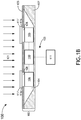
- FIG. 1A illustrates a conceptual view of a cross-section of the measurement wafer device 100 for measuring radiation and/or temperature at one or more locations across the wafer device, in accordance with one or more embodiments of the present disclosure.
- the wafer measurement device 100 includes a wafer assembly 102.
- the wafer assembly 102 includes one or more cavities 104.
- the one or more cavities 104 may be formed by any process known in the art of semiconductor fabrication (e.g., grinding, chemical etching, laser etching and the like).
- the wafer measurement device 100 includes detector assembly 103 disposed within the cavity 104 of the wafer assembly 102. It is noted herein that the present disclosure is not limited to a wafer assembly 102 including one or more cavities 104.
- the detector assembly 103 (or portions thereof) need not be disposed within a cavity 104, but may be disposed on any surface (e.g., top surface, bottom surface or edge) of the wafer assembly 102.
- the detector assembly 103 includes one or more light sensors 106.
- the one or more light sensors 106 may include any light sensor known in the art.
- the one or more light sensors 106 may include, but are not limited to, a light sensor capable of sensing UV and/or visible light.
- the detector assembly 103 is configured to perform a direct measurement of the intensity of ultraviolet light incident on at least one surface of the wafer assembly.
- the one or more light sensors 106 may include, but are not limited to, one or more light sensors sensitive to at least UV light (e.g., silicon carbide based sensor).
- the light sensors may include, but are not limited to, light sensors sensitive to UV light in the wavelength range of 150-400 nm.
- the detector assembly 103 is configured to perform an indirect measurement of the intensity of ultraviolet light incident on the at least one surface of the wafer assembly.
- the one or more light sensors 106 may include, but are not limited to, one or more light sensors sensitive to at least visible light (e.g., silicon based sensor).
- the light sensors may include, but are not limited to, light sensors sensitive to visible light in the wavelength range of 450-750 nm.
- an "indirect measurement” is interpreted as a measurement of light intensity involving an intermediate conversion of a light signal from a first wavelength/wavelength range to a second wavelength/wavelength range, such as, but not limited to, photoluminescence conversion of UV light to visible light. Further, the term “direct measurement” is interpreted as a measurement of light intensity not involved an intermediate conversion of a light signal. It is noted that embodiments associated with direct intensity measurement ( FIGS. 1B-1D ) and embodiments associated with indirect intensity measurement ( FIGS. 1E-1H ) are described in additional detail further herein.
- the one or more light sensors 106 include one or more diode detectors.
- the one or more light sensors 106 may include, but are not limited to, one or more silicon carbide (SiC) diode detectors, one or more gallium nitride (GaN) diode detectors, one or more aluminum gallium nitride (AIGaN) detectors or one or more silicon diode detectors.
- the wafer assembly 102 includes one or more openings 108.
- the one or more openings 108 are formed at the top surface of the wafer assembly 102 so as to allow ultraviolet light 101 incident on the top surface of the wafer assembly 102 to the one or more light sensors 106.
- the one or more openings 108 may be distributed across the top surface of the wafer assembly so as to allow for the selected measurement of intensity and/or temperature across the surface of the wafer assembly 102.
- the detector assembly 103 of the wafer measurement device 100 includes a local controller 110.
- the local controller 110 is communicatively coupled to the one or more light sensors 106.
- the local controller 110 may receive one or more signals from the one or more sensors 106 indicative of the intensity of light measured by the one or more light sensors 106 or one or more additional characteristics of the one or more light sensors 106.
- the local controller 110 may receive one or more signals from the one or more light sensors 106 indicative of the intensity of the light (e.g., UV or visible light) measured by the one or more light sensors 106.
- the local controller 110 may receive one or more signals from the one or more light sensors 106 indicative of one or more electrical characteristics (e.g., voltage output) of the one or more light sensors 106.
- the device 100 monitors the temperature of the wafer assembly 102 at the one or more light sensors 106 by measuring one or more electrical characteristics (e.g., forward voltage) of the one or more sensors 106.
- the detector assembly 103 includes one or more temperature sensors (e.g., thermal probes). The thermal probes may be disposed proximate to the one or more light sensors 106, with the output of the thermal probes being coupled to the one or more local controllers 110.
- temperature across the wafer assembly 102 may be measured via the decay of PL emission intensity measured by light sensors 106 (indirect measurement case), via one or more electrical characteristics of the light sensors 106 (direct measurement case), or via a dedicated temperature probe (direct measurement or indirect measurement cases).
- the detector assembly 103 of the wafer measurement device 100 includes a central controller 111.
- the central controller 111 is configured to determine a temperature of one or more portions of the wafer assembly 102 based on one or more characteristics of the one or more sensors 106 (e.g., a characteristic of the intensity of the PL emission incident or an electrical characteristic of the one or more sensors 106).
- the central controller 111 may determine a temperature of one or more portions of the wafer assembly 102 based on an electrical characteristic (e.g., forward voltage across a given sensor 106 at a known current) measured at the one or more light sensors 106.
- the central controller 111 may determine a temperature of one or more portions of the wafer assembly 102 based on a measured intensity characteristic (e.g., light intensity values at different excitation wavelengths or intensity decay time - in the case of intermediate PL elements) from the one or more sensors 106. Then, based on the measured electrical characteristics or intensity characteristics from the one or more light sensors 106 or the temperature measurement from the dedicated temperature sensors one or more temperature values may be determined.
- an electrical characteristic e.g., forward voltage across a given sensor 106 at a known current
- the central controller 111 may determine a temperature of one or more portions of the wafer assembly 102 based on a measured intensity characteristic (e.g., light intensity values at different excitation wavelengths or intensity decay time - in the case of intermediate
- the UV intensity and/or the calculated temperature may be mapped to the wafer device position based on the position of the light sensor 106 (or the position of the PL element, in the case of indirect conversion). Applying this procedure for each of the light sensors 106 distributed across the wafer assembly 102 a 2D intensity and/or temperature map may be generated by the detector assembly 103 (e.g., generated by the central controller 111).
- device 100 is not limited to measurement contexts that include both intensity and temperature.
- the device 100 may be configured to measure intensity of light alone, temperature exposure alone or intensity and temperature.
- the local controller 110 and/or the central controller 111 include one or more processors (not shown).
- the one or more processors are configured to execute a set of program instructions configured to cause the one or more processors to carry out one or more of the various steps described throughout the present disclosure.
- the controller 110 may include a non-transitory medium (e.g., memory medium) for storing the program instructions and the intensity measurement results received from the one or more sensors 106.
- the term 'processor' may be broadly defined to encompass any device having one or more processors (e.g., CPU) or logic elements (e.g., ASICs), which execute instructions from a memory medium.
- the one or more processors of local controller 110 and/or central controller 111 may include any microprocessor-type or logic device configured to execute algorithms and/or instructions. It should be recognized that the steps described throughout the present disclosure may be carried out by a single processor or, alternatively, multiple processors.
- the memory medium may include a read-only memory, a random access memory, a magnetic or optical disk, a solid state drive, flash, EPROM, EEPROM, a magnetic tape or the like.
- FIGS. 1B-1E illustrate simplified cross-sectional, assembly and top views of the measurement wafer device 100 for measuring radiation intensity and temperature via direct light intensity measurement, in accordance with one or more embodiments of the present disclosure. It is noted herein that the description of the components and embodiments illustrated in FIG. 1A should be interpreted to extend to FIGS. 1B-1E unless noted otherwise.
- the wafer assembly 102 of the measurement wafer device 100 includes one or more structures.
- the one or more light sensors 106 are disposed within the one or more structures of the measures wafer device 100.
- structures of the measurement wafer device 100 may be arranged and/or formed so as to form the one or more cavities 104.
- the wafer assembly 102 may fit within a thin form factor package. It is noted herein that the sensor wafer 102 is designed to mimic a wafer typically used in a processing environment within the semiconductor industry (e.g., plasma processing device) in order to provide insight as to the intensity of UV light and temperature exposure of a wafer undergoing the conditions in the given processing environment.
- the wafer assembly 102 includes a substrate 107 (e.g., substrate wafer).
- the substrate may be formed from any material known in the art compatible with semiconductor device processing steps.
- substrate 107 may include, but is not limited to, a semiconductor substrate, a glass substrate and the like.
- the measurement wafer device 100 includes a cover 103 (e.g., cover wafer).
- cover 103 may be attachable to the top surface of the substrate 105.
- the one or more cavities 104 of the wafer assembly 102 are formed between the substrate 105 and cover 103.
- the substrate 105 may include a recessed portion, as shown in FIG. 1B and 1C .
- the recessed portion of the substrate 105 and the cover 103 may form one or more cavities 104 within the wafer assembly 102.
- the one or more cavities 104 of the wafer assembly 102 may be formed by any processing procedure known in the art.
- the process used to form the cavity 104 may include, but is not limited to, a mechanical grinding process, an etching process or a laser machining process performed on the substrate to form one or more recessed portions in the substrate 105.
- the cavity 104 may have a substantially truncated conical shape, as shown in FIGS. 1B and 1C . It is noted herein that the shape depicted in FIGS. 1B and 1C is not limiting and is provided merely for illustrative purposes. It is noted herein that the cavity 104 depicted in FIGS. 1B and 1C is not a limitation on the present disclosure and is provided merely for illustrative purposes. The cavity 104 may take on any shape known in the art.
- the cavity 104 may have a shape including, but not limited to, a truncated conic section, a cuboid, a cylinder (e.g., shallow cylinder), a prism (e.g., triangular prism, a hexagonal prism and the like) and similar shapes.
- the wafer assembly 102 may include any cavity arrangement or number of cavities suitable for housing the various components (e.g., light sensor(s) 106, controller 110 and the like) within the wafer assembly 102.
- one or more openings 108 are formed in the cover 105.
- one or more openings 108 are arranged so as to transmit light (e.g., UV light) from the top surface of the cover 105 to one or more sensors 106 situated below the top cover 105.
- the one or more openings 108 may be distributed across the top surface of the wafer assembly so as to allow for the selected measurement of intensity, temperature across the surface of the wafer assembly 102.
- the light sensors 106 may be arranged so a light sensor 106 is positioned proximate to each of the openings 108, creating a network of light sensors 106 distributed across the wafer assembly 102, thereby allowing for the analysis of intensity, temperature uniformity across the wafer assembly 102.
- the wafer assembly 102 includes one or windows 116.
- the one or more windows 116 are positioned above, below or within the one or more openings 108.
- the wafer assembly 102 includes one or more entrance filters 117.
- the one or more entrance filters 117 are disposed proximate to the one or more windows 116 and are configured to block a portion of light 101 incident on the surface of the wafer assembly 102.
- the one or more entrance filters 117 may be selected so as to block visible light or IR light to avoid false positives at the one or more light sensors 106.
- one or more windows 116 at the openings 108 serves to protect the one or more sensors 106 (and other electronics) within the wafer assembly 102 from the harsh conditions associated with the processing environment above the wafer assembly 102.
- the one or more windows 116 may serve as support structures for supporting thin film filters (e.g., dielectric filter).
- the one or more light sensors 106 may include one or more diode detectors.
- diode detectors sensitive to UV are particularly useful. While the diode detectors of this embodiment are not limited to any particular type of diode detectors, diode detectors, such as, but not limited to, SiC and GaN display UV light and display sensitivity features suitable for use in the direct measurement of UV light.
- the local controller 110 receives one or more signals from one or more light sensors 106 indicative of the intensity of UV light measured by the one or more light sensors 106. Further, the local controller 110 receives one or more signals from one or more light sensors 106 indicative of one or more electrical characteristics of one or more light sensors 106. In turn, the central controller 111 may determine the temperature of the one or more sensors 106 based on the intensity of the ultraviolet light 101 measured by the one or more light sensors 106 and/or one or more electrical characteristics of the one or more light sensors 106. It is noted that various electrical characteristics of a diode detector, such as, but not limited to, forward voltage (e.g., forward voltage measured at a known current), may vary as a function of temperature. In this regard, the central controller 111 may correlate the measured electrical characteristic to the temperature of the one or more diode-based light sensors 106.
- forward voltage e.g., forward voltage measured at a known current
- the detector assembly 103 includes one or more dedicated temperature sensors. While the one or more temperature sensors are not depicted in FIGS. 1B-1C for purposes of clarity, the one or more temperature sensors may be positioned on or proximate to the one or more light sensors 106. For instance, in FIG. 1B , the one or more temperature sensors may be positioned adjacent to, under or on the top surface of the one or more light sensors 106. Further, the output of the one or more temperature sensors may be coupled to the one or more local controllers 110. It is noted herein that one or more dedicated temperature sensors may be used in the context of either the direct measurement approach or the indirect measurement approach of the present disclosure. The one or more temperature sensors may include any temperature sensor know in the art. For example, the one or more temperature sensors may include, but are not limited to, a RTD, a thermocouple device and the like.
- a given local controller 110 is positioned proximate to the one or more light sensors 106 coupled to the given local controller 110. Such a configuration may be suitable for use in low temperature applications (e.g., applications less than 150° C).
- a given local controller 110 is positioned remotely from the one or more light sensors 106 coupled to the given local controller 110. In this embodiment, the given local controller 110 may be thermally isolated from the substrate. Such a configuration may be suitable for use in high temperature applications (e.g., greater than 150° C) and serves to protect sensitive electronics in the local controller 111 from high temperatures.
- the one or more local controllers 110 may include any necessary electronic components known in the art of data processing and communication. Further, one or more batteries (not shown) may be housed within the one or more local controller 110 so as to protect the one or more batteries from high temperatures.
- multiple light sensors 106 are coupled to a single local controller 110.
- the measurement wafer device 100 includes multiple detector assemblies 103.
- the measurement wafer device 100 may include multiple local controllers 110, with each local controller 110 being coupled to multiple light sensors 106. This arrangement forms a distributed network of light sensors 106 capable of monitoring the spatial and temporal dependence of light intensity and temperature across the wafer assembly 102.
- the one or more local controllers 110 are wirelessly communicatively coupled to the central controller 111.
- the one or more local controllers 110 may be wirelessly communicatively coupled to the central controller 111 in any suitable manner.
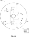
- the measurement wafer device 100 includes a communication coil 120.
- the one or more local controllers 110 are communicatively coupled to the communication coil (e.g., coupled via electrical interconnect 118).
- the communication coil 120 establishes a wireless communication link between the one or more local controllers 110 and the central controller 111.
- the communication coil 120 may establish a wireless communication link with the communication circuitry 122 of the central controller 111.
- the communication coil 120 may be used to transmit one or more signals (e.g., RF signals) indicative of the intensity measurements and/or electrical characteristic measurements (and/or temperature measurements from dedicated temperature sensor) from the one or more light sensors 106.
- the central controller 111 may determine the temperature of the one or more light sensors 106 (which may be correlated to the corresponding position on the surface of the wafer assembly 102) based on one or more characteristics or features of the one or more electrical characteristics of the one or more light sensors 106 (and/or the temperature measurements from dedicated temperature sensor).
- FIGS. 1E-1I illustrate various views of the measurement wafer device 100 for measuring UV light intensity and temperature via an indirect light intensity measurement, in accordance with one or more embodiments of the present disclosure. It is noted herein that the description of the components and embodiments illustrated in FIGS. 1A-1D should be interpreted to extend to FIGS. 1E-1I unless otherwise noted.
- the detector assembly 103 includes one or more photoluminescent (PL) elements 112. It is noted that the one or more PL elements 112 are suitable for absorbing at least UV light and, in response to UV absorption, emit at least visible light. Such a configuration allows for the use of light sensors that normally have less than desired sensitivity to UV light.
- the one or more PL elements 112 of the detector assembly 103 may be used to convert at least some of the UV light incident on the PL elements 112 to visible light, which in some instances is more readily detected by certain sensor types (e.g., silicon diode detectors). For example, silicon diode detectors are commonly weakly sensitive to light having a wavelength below 350 nm.
- the detector assembly 103 determines the temperature of the one or more PL elements 112 based on an intensity feature of the intensity of the PL light measured by the one or more light sensors 106.
- the intensity feature may include, but is not limited to, a decay feature (e.g., decay time) of the intensity of the PL light measured by the one or more light sensors 106.
- the central controller 111 may calculate the temperature corresponding with a given PL element 112 based on the decay time of the intensity of PL light measured from the given PL element 112.
- a decay-based measurement may require discontinuous excitation light (e.g., UV light), so as to allow for the proper characterization of the emission decay.
- discontinuous excitation light e.g., UV light
- the exponential decay of the emission intensity from phosphors often displays strong temperature dependence. This effect is known as "phosphor thermometry.”
- one or more features/characteristics of the decay behavior of a given PL emission event of a PL element 112 may be used to calculate the temperature of the given PL element 112.
- the decay time of the emission intensity of a given PL emission event of a PL element 112 may be used to calculate the temperature of the given PL element 112.
- the intensity feature may include, but is not limited to, a ratio of the intensity of the PL light as measured by the one or more sensors to the intensity of PL measured at a known temperature.
- the central controller 111 may calculate the temperature corresponding with a given PL element 112 based on the decay time of the intensity of PL light measured from the given PL element 112 or the calculated ratio of the measured PL light intensity to a PL light intensity measured at a known temperature for the given PL element 112.
- the one or more PL elements include any PL element known in the art.
- the one or more PL elements may be formed from, but are not limited to, a phosphor material or a blend of phosphor materials.
- the one or more PL elements are formed by forming a layer of phosphor and/or phosphor blend on a surface of a substrate.
- the one or more PL elements are formed by forming a layer of phosphor and/or phosphor blend on a surface of a portion of the substrate 107 of the wafer assembly 103.
- the indirect light intensity/temperature measurement described herein may be implemented both in low and high temperature regimes.
- the one or more light sensors 106 and other additional electronic components e.g., local controller
- the one or more light sensors 106 and additional electronic components may be disposed on (or at least near) the substrate 107.
- the one or more PL elements 112 are affixed or positioned proximate to the one or more light sensors 106.
- the one or more PL elements may be disposed at the top surface of the one or more light sensors 106.
- FIG. 1F a sensor stack 119 is illustrated.
- the sensor stack 119 includes a PL element 112 disposed on the top surface of a light sensor 106.
- the sensor stack 119 is coupled to one or more local controllers (not shown in FIG. 1F ) via an electrical interconnect 118.
- the one or more sensor stacks 119 may be arranged in a manner similar to the sensor arrangements described with respect to FIGS.
- the one or more sensors will detect light emitted from the PL elements 112. Then, the one or more local controllers 110 (or the central controller 111) may correlate the intensity of PL light from the PL elements 112 to the intensity of UV light impinging on the PL elements 112. In turn, the central controller 111 may then calculate the temperature of the one or more PL elements 112 based on an intensity feature of the PL light measured by the one or more light sensors 106.
- emission of the one or more PL elements 112 may be coupled to the one or more sensors 106 via free space coupling (not shown).
- the light emitted by the one or more PL elements travels, in free space (or a selected atmosphere), to the one or more sensors 106.
- the one or more light sensors 106, the local controller 110 and/or other additional electronic components are housed in a sensor module 114.
- the sensor module 114 is thermally isolated from the substrate 107 of the wafer assembly 102.
- the detector assembly 103 includes one or more light guiding elements 113 disposed within the one or more cavities 104.
- the one or more light guiding elements 113 are arranged to transmit light emitted by the one or more PL elements 112 to the one or more light sensors 106.
- the emission of the one or more PL elements 112 is coupled to the one or more sensors 106 via one or more light guiding elements 113.
- visible light emitted by the one or more PL elements 112 may be transmitted along the one or more light guiding elements 113 to the one or more sensors 106 housed in the sensor module 114.
- the one or more local controllers 110 may correlate the intensity of the visible PL light to the intensity of UV light impinging on the PL elements 112 (through opening(s) 108).
- the central controller 111 may then calculate the temperature of the one or more PL elements 112 based on an intensity feature of the intensity of the visible PL light measured by the one or more light sensors 106.
- the one or more light guiding elements 113 may include any light guiding element known in the art.
- the one or more light guiding elements 113 include an optical light guide.
- the one or more light guiding elements 113 may include, but are not limited to, an optical light guide formed from glass, quartz, sapphire, acrylic and the like.
- the one or more light guiding elements 113 may include, but are not limited to, an optical fiber or an optical fiber bundle.
- the wafer assembly 102 is constructed such that the one or more cavities 104 consist of one or more channels that conform to the one or more light guiding elements 113.
- the one or more light guiding elements 113 may provide mechanical support to the sensor module 114 so as to assist in securing the sensor module 114 above the top surface of the wafer assembly 102. It is noted that, in the case of a rigid light guide (e.g., glass, acrylic, quartz, sapphire rod), the light guiding element 113 is particularly useful for supplying mechanical support to the sensor module 114 due to the rigidity of the light guide and the low thermal conductivity.
- a rigid light guide e.g., glass, acrylic, quartz, sapphire rod
- the detector assembly 103 includes one or more sensor filters (not shown).
- a sensor filter may be positioned at the entrance of the one or more light sensors 106.
- a sensor filter may be positioned between the output of a given light guiding element 113 and the entrance to a corresponding light sensor 106.
- the one or more sensor filters may be selected so as to filter out undesired light from detection by the one or more light sensors 106.
- the one or more sensor filters may include, but are not limited to, a filter capable of blocking excitation light (e.g., UV light) entering the wafer assembly cavity 102 via openings 108.
- the one or more sensor filters may include, but are not limited to, one or more filters that selectively pass the PL emission (or a portion of the PL emission) from the one or more PL elements 112 to the one or more light sensors 106.
- the detector assembly 103 includes multiple light guiding elements 113.
- multiple light guiding elements 113 may serve to couple the PL emission from multiple PL elements 112 to multiple light sensors 106 housed within a single sensor module 114.
- FIG. 1H illustrates a cross-sectional view of the measurement wafer device 100 with multiple light guiding elements 113 coupling the output of one or more PL elements 112 to the multiple sensors 106.
- each PL element 112 is coupled to a single light sensor 106.
- multiple PL elements 112 are coupled to a single light sensor 106.
- the multiple light guiding elements 113 serve to elevate the sensor module 114 from the wafer assembly 102.
- FIG. 1I illustrates top view of the substrate 107 of the wafer assembly 102 of the measurement wafer device 100 with multiple light guiding elements 113 coupling the output of one or more PL elements 112 to the multiple sensors 106, in accordance with one embodiment of the present disclosure. It is noted that the cover 105 is not depicted in FIG. 1I for purposes of clarity. In one embodiment, multiple PL elements 112 (e.g., phosphor dots) are distributed across the substrate 107 of the wafer assembly 102. Further, the device 100 includes multiple sensor modules 114. Each of the multiple sensor modules 114 includes one or more light sensors 106 (not shown in FIG.
- a set of light guiding elements 113 serve to transmit light (e.g., visible light) from each of a group of PL elements 112 to the associated sensor module 114.
- cover 105 is not depicted in FIG. 1I for purposes of clarity, it is further noted that the PL elements 113 distributed across the substrate 107 may be covered by windows 116 disposed on/in the cover 105 that sits above the substrate. In this regard, the cover 105 may have a window pattern that corresponds to the pattern of PL elements 112 distributed across the substrate 107.
- the measurement wafer device also includes one or more communication coils 120 suitable for establishing a communication link between the sensor modules 114 and the central controller 111 (e.g., communication circuitry 122 of central controller 111).
- the present disclosure has focused on the temperature determination being carried out by the central controller 111, this is not a limitation on the present disclosure. It is recognized herein that the temperature calculation of the present disclosure may be carried out on the one or more local controllers 110 (or any additional controller or processing element). In general, it is noted that the various data processing steps (or portions of the various data processing steps) of the present disclosure may be carried out on either the one or more local controllers 110 or the central controller 111.
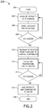
- FIG. 2 is a flowchart depicting the method 200 of measuring radiation intensity and temperature across the measurement wafer 100, in accordance with one embodiment of the present disclosure. It is noted herein that the steps of flow chart 200 are not to be interpreted as limiting and are provided merely for illustrative purposes.
- the process starts at step 202.
- the process includes measuring the intensity of UV light at an ith sensor of the one or more sensors 106.
- UV light intensity may be measured directly (e.g., UV light passed through openings 108 is measured by sensors 106) or indirectly (e.g., visible PL light emitted in response to UV light absorption is measured by sensors 106).
- the result is stored in memory (e.g., memory of local controller 110).
- step 208 if the ith sensor is not last sensor of the one or more sensors 106 then the NO branch is taken and steps 204, 206 are repeated. In the case where the ith sensor is the last sensor of the one or more light sensors 106 then the YES branch is taken and the process moves to step 210.
- step 210 the measurement data acquired and stored from the N sensors (e.g., stored in one or more local controllers 110) is transmitted to the central controller 111.
- the temperature is calculated for the ith sensor of the one or more sensors 106.
- the temperature associated with the ith sensor may be calculated based on an intensity feature of the measured intensity (e.g., decay time of visible intensity in case of indirect measurement).
- the temperature associated with the ith sensor may be calculated based on one or more measured electrical characteristics of the one or more sensors 106 (e.g., forward voltage of the one or more sensors).
- the temperature associated with the ith sensor may be measured using a dedicated ith temperature sensor.
- step 214 if the ith sensor is not last sensor of the one or more sensors 106 then the NO branch is taken and step 212 is repeated. In the case where the ith sensor is the last sensor of the one or more light sensors 106 then the YES branch is taken and the process moves to step 216.
- the intensity and/or temperature results for each of the N sensors is mapped to the surface of the wafer assembly 102.
- the central controller 111 (or another controller) may correlate the intensity and/or temperature measured for each sensor of the one or more sensors 106. Then, based on the known position of each of the light sensors 106 (or the position of each of the PL elements 112 in the case of the indirect measurement approach) the central control 111 can form a database and/or map of the intensity and/or temperature at the top surface of the wafer assembly 102 as a function of position in the plane of the top surface (e.g., X-Y position) of the wafer assembly 102. In another embodiment, the database and/or map of the intensity and/or temperature is presented on a display of a user interface (not shown).
- any two components herein combined to achieve a particular functionality can be seen as “associated with” each other such that the desired functionality is achieved, irrespective of architectures or intermedial components.
- any two components so associated can also be viewed as being “connected”, or “coupled”, to each other to achieve the desired functionality, and any two components capable of being so associated can also be viewed as being “couplable”, to each other to achieve the desired functionality.
- Specific examples of couplable include but are not limited to physically interactable and/or physically interacting components and/or wirelessly interactable and/or wirelessly interacting components and/or logically interactable and/or logically interacting components.
Landscapes
- Physics & Mathematics (AREA)
- General Physics & Mathematics (AREA)
- Spectroscopy & Molecular Physics (AREA)
- Photometry And Measurement Of Optical Pulse Characteristics (AREA)
- Testing Or Measuring Of Semiconductors Or The Like (AREA)
- Measuring Temperature Or Quantity Of Heat (AREA)
- Radiation Pyrometers (AREA)
Claims (7)
- Messwafervorrichtung (100) zum Messen von Strahlungsintensität und Temperatur, die Folgendes umfasst:eine Waferbaugruppe (102), die einen oder mehrere Hohlräume (104) beinhaltet; undeine Detektorbaugruppe (103), wobei die Detektorbaugruppe innerhalb des einen oder der mehreren Hohlräume (104) der Waferbaugruppe angeordnet ist, wobei die Detektorbaugruppe einen oder mehrere Lichtsensoren (106) beinhaltet, wobei der eine oder die mehreren Lichtsensoren (106) einen oder mehrere Diodendetektoren beinhalten, wobei die Detektorbaugruppe dazu konfiguriert ist, eine direkte Messung der Intensität von ultraviolettem Licht, das auf mindestens eine Oberfläche der Waferbaugruppe (102) einfällt, durchzuführen, wobei die direkte Messung eine Messung der Lichtintensität von ultraviolettem Licht, das auf mindestens eine Oberfläche der Waferbaugruppe (102) einfällt, umfasst, die keine dazwischenliegende Umwandlung eines Lichtsignals von einer ersten Wellenlänge in eine zweite Wellenlänge involviert, wobei die Detektorbaugruppe (103) ferner dazu konfiguriert ist, eine Temperatur eines oder mehrerer Abschnitte der Waferbaugruppe (102) auf Grundlage einer oder mehrerer Eigenschaften des einen oder der mehreren Lichtsensoren (106) beim Messen der Intensität des ultravioletten Lichts, das auf die mindestens eine Oberfläche der Waferbaugruppe (102) einfällt, zu bestimmen;wobei die eine oder mehreren Eigenschaften des einen oder der mehreren Lichtsensoren (106) Folgendes umfassen:eine elektrische Eigenschaft des einen oder der mehreren Lichtsensoren (106);wobei die elektrische Eigenschaft Folgendes umfasst:eine Durchlassspannung über den einen oder die mehreren Lichtsensoren (106), gemessen bei einem bekannten Strom;wobei die Waferbaugruppe (102) eine oder mehrere Öffnungen (108) an der mindestens einen Oberfläche der Waferbaugruppe (102) beinhaltet, die dazu konfiguriert sind, ultraviolettes Licht, das auf die mindestens eine Oberfläche der Waferbaugruppe (102) einfällt, zu dem einen oder den mehreren Lichtsensoren (106) der Detektorbaugruppe (103) durchzuleiten.
- Vorrichtung nach Anspruch 1, wobei die Waferbaugruppe (102) Folgendes umfasst:ein Substrat (105); undeine Abdeckung, die an einen Abschnitt des Substrats (105) wirkgekoppelt ist.
- Vorrichtung nach Anspruch 1, wobei der eine oder die mehreren Lichtsensoren (106) dazu konfiguriert sind, eine direkte Messung der Intensität von ultraviolettem Licht, das auf den einen oder die mehreren Lichtsensoren (106) einfällt, durchzuführen.
- Vorrichtung nach Anspruch 1, wobei die Detektorbaugruppe (103) Folgendes umfasst:eine lokale Steuerung (110), die dazu konfiguriert ist, ein oder mehrere Signale von dem einen oder den mehreren Lichtsensoren (106) zu empfangen, die eine elektrische Eigenschaft des einen oder der mehreren Lichtsensoren (106) angeben; undeine zentrale Steuerung (111), die kommunikativ an die lokale Steuerung (110) gekoppelt und dazu konfiguriert ist, eine Temperatur des einen oder der mehreren Abschnitte der Waferbaugruppe (102) auf Grundlage einer elektrischen Eigenschaft des einen oder der mehreren Lichtsensoren (106) zu bestimmen.
- Vorrichtung nach Anspruch 1, wobei die Waferbaugruppe (102) ein oder mehrere Fenster (116) beinhaltet, die an der einen oder den mehreren Öffnungen (116) an der mindestens einen Oberfläche der Waferbaugruppe (102) positioniert und dazu konfiguriert sind, ultraviolettes Licht, das auf die mindestens eine Oberfläche der Waferbaugruppe (102) einfällt, zu dem einen oder den mehreren Lichtsensoren (106) der Detektorbaugruppe (103) zu übertragen.
- Vorrichtung nach Anspruch 5, wobei die Waferbaugruppe (102) ein oder mehrere Eingangsfilter (117) beinhaltet, die zumindest nahe des einen oder der mehreren Fenster (116) angeordnet und dazu konfiguriert sind, einen ausgewählten Teil des Lichts, das auf die mindestens eine Oberfläche der Waferbaugruppe (102) einfällt, zu blockieren.
- Vorrichtung nach Anspruch 1, wobei der eine oder die mehreren Diodendetektoren Folgendes umfassen:
mindestens einen von einem Siliziumkarbid-Detektor, einem Galliumnitrid-Diodendetektor, einem Aluminium-Galliumnitrid-Detektor oder einem Siliziumdetektor.
Applications Claiming Priority (3)
| Application Number | Priority Date | Filing Date | Title |
|---|---|---|---|
| US201462063657P | 2014-10-14 | 2014-10-14 | |
| US14/880,899 US9823121B2 (en) | 2014-10-14 | 2015-10-12 | Method and system for measuring radiation and temperature exposure of wafers along a fabrication process line |
| PCT/US2015/055307 WO2016061089A1 (en) | 2014-10-14 | 2015-10-13 | Method and system for measuring radiation and temperature exposure of wafers along a fabrication process line |
Publications (3)
| Publication Number | Publication Date |
|---|---|
| EP3201942A1 EP3201942A1 (de) | 2017-08-09 |
| EP3201942A4 EP3201942A4 (de) | 2018-06-20 |
| EP3201942B1 true EP3201942B1 (de) | 2021-09-22 |
Family
ID=55747214
Family Applications (1)
| Application Number | Title | Priority Date | Filing Date |
|---|---|---|---|
| EP15851269.9A Active EP3201942B1 (de) | 2014-10-14 | 2015-10-13 | Messwafer zum messen der strahlungs- und temperaturexposition von wafern entlang einer herstellungsprozesslinie |
Country Status (7)
| Country | Link |
|---|---|
| US (2) | US9823121B2 (de) |
| EP (1) | EP3201942B1 (de) |
| JP (3) | JP6738327B2 (de) |
| KR (1) | KR102290939B1 (de) |
| CN (2) | CN106796903B (de) |
| TW (1) | TWI685907B (de) |
| WO (1) | WO2016061089A1 (de) |
Families Citing this family (17)
| Publication number | Priority date | Publication date | Assignee | Title |
|---|---|---|---|---|
| SG11201708481TA (en) * | 2015-04-15 | 2017-11-29 | Razer (Asia-Pacific) Pte Ltd | Filtering devices and filtering methods |
| WO2018054471A1 (en) * | 2016-09-22 | 2018-03-29 | Applied Materials, Inc. | Carrier for supporting a substrate, apparatus for processing a substrate and method therefore |
| US20180366354A1 (en) * | 2017-06-19 | 2018-12-20 | Applied Materials, Inc. | In-situ semiconductor processing chamber temperature apparatus |
| US10512704B2 (en) * | 2017-06-27 | 2019-12-24 | The Boeing Company | Cleanliness indication systems and methods |
| US11655992B2 (en) * | 2018-02-13 | 2023-05-23 | Advanced Semiconductor Engineering, Inc. | Measuring system |
| US10916411B2 (en) | 2018-08-13 | 2021-02-09 | Tokyo Electron Limited | Sensor-to-sensor matching methods for chamber matching |
| CN112437975B (zh) * | 2018-08-22 | 2024-08-09 | 玛特森技术公司 | 在低温下对工件进行热处理和温度测量的系统和方法 |
| US11315811B2 (en) * | 2018-09-06 | 2022-04-26 | Kla Corporation | Process temperature measurement device fabrication techniques and methods of calibration and data interpolation of the same |
| JP7108562B2 (ja) * | 2019-02-22 | 2022-07-28 | 株式会社日立製作所 | 処理の制御パラメータの決定方法、及び計測システム |
| CN114222951B (zh) | 2019-08-14 | 2024-10-08 | Asml控股股份有限公司 | 光刻设备和紫外辐射控制系统 |
| KR102405796B1 (ko) | 2020-01-22 | 2022-06-08 | 한국원자력연구원 | 표면오염물질 채취 장치 |
| US11668601B2 (en) | 2020-02-24 | 2023-06-06 | Kla Corporation | Instrumented substrate apparatus |
| JP7580321B2 (ja) * | 2021-03-29 | 2024-11-11 | 東京エレクトロン株式会社 | 計測装置、基板処理装置、及び計測方法 |
| US11688614B2 (en) | 2021-04-28 | 2023-06-27 | Kla Corporation | Mitigating thermal expansion mismatch in temperature probe construction apparatus and method |
| CN116968506A (zh) * | 2023-08-30 | 2023-10-31 | 中国第一汽车股份有限公司 | 用于车辆的座椅组件及车辆 |
| US20250137844A1 (en) * | 2023-11-01 | 2025-05-01 | Kla Corporation | Metrology method of calibrating and monitoring radiation in euv lithographic systems |
| US20250239473A1 (en) * | 2024-01-18 | 2025-07-24 | Kla Corporation | Process condition measurement device including thermally isolated electronic modules |
Family Cites Families (37)
| Publication number | Priority date | Publication date | Assignee | Title |
|---|---|---|---|---|
| US4215275A (en) | 1977-12-07 | 1980-07-29 | Luxtron Corporation | Optical temperature measurement technique utilizing phosphors |
| US4459044A (en) | 1981-02-09 | 1984-07-10 | Luxtron Corporation | Optical system for an instrument to detect the temperature of an optical fiber phosphor probe |
| JPS58143542A (ja) * | 1982-02-22 | 1983-08-26 | Toshiba Corp | 半導体単結晶の評価方法 |
| JPH0456145A (ja) * | 1990-06-22 | 1992-02-24 | Hitachi Ltd | プラズマ中の基板温度の測定装置 |
| US5470155A (en) | 1993-06-11 | 1995-11-28 | Luxtron Corporation | Apparatus and method for measuring temperatures at a plurality of locations using luminescent-type temperature sensors which are excited in a time sequence |
| US5414266A (en) | 1993-06-11 | 1995-05-09 | Luxtron Corporation | Measuring system employing a luminescent sensor and methods of designing the system |
| JPH07134069A (ja) * | 1993-11-10 | 1995-05-23 | Hitachi Ltd | 基板温度のモニタ方法 |
| JP3868056B2 (ja) * | 1997-05-07 | 2007-01-17 | 株式会社ディスコ | ウェーハのチッピング検出方法 |
| JP3890131B2 (ja) * | 1997-12-17 | 2007-03-07 | キヤノン株式会社 | 露光装置およびデバイス製造方法 |
| US6183130B1 (en) * | 1998-02-20 | 2001-02-06 | Applied Materials, Inc. | Apparatus for substrate temperature measurement using a reflecting cavity and detector |
| JP2001215153A (ja) * | 2000-02-01 | 2001-08-10 | Omron Corp | 透明体検出装置 |
| JP2001330513A (ja) * | 2000-05-19 | 2001-11-30 | Tokyo Electron Tohoku Ltd | 温度測定方法および温度測定装置および半導体製造装置 |
| US7080940B2 (en) | 2001-04-20 | 2006-07-25 | Luxtron Corporation | In situ optical surface temperature measuring techniques and devices |
| JP2002344001A (ja) | 2001-05-18 | 2002-11-29 | Fuji Xerox Co Ltd | 波長分離型紫外線受光器 |
| US7757574B2 (en) * | 2002-01-24 | 2010-07-20 | Kla-Tencor Corporation | Process condition sensing wafer and data analysis system |
| US7217588B2 (en) | 2005-01-05 | 2007-05-15 | Sharp Laboratories Of America, Inc. | Integrated MEMS packaging |
| US6828542B2 (en) | 2002-06-07 | 2004-12-07 | Brion Technologies, Inc. | System and method for lithography process monitoring and control |
| FR2844635B1 (fr) * | 2002-09-16 | 2005-08-19 | Commissariat Energie Atomique | Dispositif detecteur de rayonnement electromagnetique avec boitier integre comportant deux detecteurs superposes |
| US6807503B2 (en) | 2002-11-04 | 2004-10-19 | Brion Technologies, Inc. | Method and apparatus for monitoring integrated circuit fabrication |
| JP4206278B2 (ja) * | 2003-01-28 | 2009-01-07 | エスアイアイ・ナノテクノロジー株式会社 | 放射線計測装置 |
| US7391147B2 (en) | 2003-12-12 | 2008-06-24 | Honeywell International Inc. | Planar ultra violet light detector |
| TWI297521B (en) * | 2004-01-22 | 2008-06-01 | Ultratech Inc | Laser thermal annealing of lightly doped silicon substrates |
| JP2008008848A (ja) * | 2006-06-30 | 2008-01-17 | Kobe Steel Ltd | 紫外線モニタリングシステム及び紫外線照射装置 |
| EP1930476A1 (de) | 2006-12-07 | 2008-06-11 | Siemens Aktiengesellschaft | Schichtsystem |
| US8104342B2 (en) * | 2007-02-23 | 2012-01-31 | Kla-Tencor Corporation | Process condition measuring device |
| CN101468344A (zh) * | 2007-12-24 | 2009-07-01 | 鸿富锦精密工业(深圳)有限公司 | 具有光强检测功能的光固化机 |
| US20100187441A1 (en) * | 2009-01-28 | 2010-07-29 | Bio-Rad Laboratories, Inc. | Transilluminator adaptor for conversion of ultraviolet radiation to visible light |
| JP5736845B2 (ja) * | 2011-03-02 | 2015-06-17 | 東レ株式会社 | 白色積層ポリエステルフィルム |
| CN202133819U (zh) * | 2011-04-25 | 2012-02-01 | 光驰科技(上海)有限公司 | 光学薄膜成膜的直接式光学监控系统 |
| CN103620779B (zh) * | 2011-07-19 | 2016-12-28 | 赫普塔冈微光有限公司 | 光电模块及其制造方法 |
| US20130026381A1 (en) * | 2011-07-25 | 2013-01-31 | Taiwan Semiconductor Manufacturing Company, Ltd. | Dynamic, real time ultraviolet radiation intensity monitor |
| US9360302B2 (en) | 2011-12-15 | 2016-06-07 | Kla-Tencor Corporation | Film thickness monitor |
| CN102645274B (zh) * | 2012-04-23 | 2015-02-11 | 南京中电熊猫液晶显示科技有限公司 | 液晶显示器背光自动调节系统用光强检测器 |
| US8753903B1 (en) * | 2012-05-22 | 2014-06-17 | Western Digital (Fremont), Llc | Methods and apparatuses for performing wafer level characterization of a plasmon element |
| US8691598B1 (en) * | 2012-12-06 | 2014-04-08 | Ultratech, Inc. | Dual-loop control for laser annealing of semiconductor wafers |
| US9322901B2 (en) * | 2013-02-20 | 2016-04-26 | Maxim Integrated Products, Inc. | Multichip wafer level package (WLP) optical device |
| JP6329790B2 (ja) * | 2014-03-25 | 2018-05-23 | 株式会社日立ハイテクノロジーズ | プラズマ処理装置 |
-
2015
- 2015-10-12 US US14/880,899 patent/US9823121B2/en active Active
- 2015-10-13 CN CN201580055146.9A patent/CN106796903B/zh active Active
- 2015-10-13 CN CN202011524836.3A patent/CN112635365B/zh active Active
- 2015-10-13 EP EP15851269.9A patent/EP3201942B1/de active Active
- 2015-10-13 JP JP2017519616A patent/JP6738327B2/ja active Active
- 2015-10-13 WO PCT/US2015/055307 patent/WO2016061089A1/en not_active Ceased
- 2015-10-13 KR KR1020177012876A patent/KR102290939B1/ko active Active
- 2015-10-14 TW TW104133752A patent/TWI685907B/zh active
-
2017
- 2017-10-12 US US15/782,692 patent/US10215626B2/en active Active
-
2020
- 2020-07-17 JP JP2020122967A patent/JP2020191458A/ja active Pending
-
2022
- 2022-05-31 JP JP2022088274A patent/JP7378538B2/ja active Active
Also Published As
| Publication number | Publication date |
|---|---|
| US9823121B2 (en) | 2017-11-21 |
| CN112635365A (zh) | 2021-04-09 |
| US20180052045A1 (en) | 2018-02-22 |
| JP2017539078A (ja) | 2017-12-28 |
| JP2022113724A (ja) | 2022-08-04 |
| EP3201942A1 (de) | 2017-08-09 |
| CN106796903B (zh) | 2021-01-08 |
| TW201614752A (en) | 2016-04-16 |
| JP6738327B2 (ja) | 2020-08-12 |
| JP2020191458A (ja) | 2020-11-26 |
| KR20170065660A (ko) | 2017-06-13 |
| WO2016061089A1 (en) | 2016-04-21 |
| CN106796903A (zh) | 2017-05-31 |
| JP7378538B2 (ja) | 2023-11-13 |
| US10215626B2 (en) | 2019-02-26 |
| US20160138969A1 (en) | 2016-05-19 |
| EP3201942A4 (de) | 2018-06-20 |
| CN112635365B (zh) | 2022-04-01 |
| KR102290939B1 (ko) | 2021-08-17 |
| TWI685907B (zh) | 2020-02-21 |
Similar Documents
| Publication | Publication Date | Title |
|---|---|---|
| EP3201942B1 (de) | Messwafer zum messen der strahlungs- und temperaturexposition von wafern entlang einer herstellungsprozesslinie | |
| CN107567590B (zh) | 用于测量电流的方法和电流传感器 | |
| CN105358949B (zh) | 用于测量热通量的方法及系统 | |
| US6140833A (en) | In-situ measurement method and apparatus for semiconductor processing | |
| KR101909319B1 (ko) | 웨이퍼 레벨 분광기 | |
| CA2786919C (en) | Photoluminescent temperature sensor utilizing a singular element for excitation and photodetection | |
| US11215509B2 (en) | Method for determining a temperature without contact, and infrared measuring system | |
| JP2009510699A (ja) | プラズマ加工の電気パラメータを測定する方法及び装置 | |
| WO2006083627A1 (en) | Plasma sensors for endpoint and end-of-life detection with self-diagnostic sensor | |
| US10591365B2 (en) | Temperature probe | |
| US11346720B2 (en) | Light measurement device and light measurement method | |
| US11150137B2 (en) | Thermal imaging with an integrated photonics chip | |
| RU2589525C1 (ru) | Способ дистанционного измерения температуры | |
| US10514418B2 (en) | Optimized wavelength photon emission microscope for VLSI devices | |
| JP2002100617A (ja) | プラズマ処理装置におけるプロセスモニター方法及びモニター装置及びそれを用いた試料の処理方法 | |
| JP5018741B2 (ja) | 半導体ウェーハの評価方法及び半導体ウェーハの評価装置 |
Legal Events
| Date | Code | Title | Description |
|---|---|---|---|
| STAA | Information on the status of an ep patent application or granted ep patent |
Free format text: STATUS: THE INTERNATIONAL PUBLICATION HAS BEEN MADE |
|
| PUAI | Public reference made under article 153(3) epc to a published international application that has entered the european phase |
Free format text: ORIGINAL CODE: 0009012 |
|
| STAA | Information on the status of an ep patent application or granted ep patent |
Free format text: STATUS: REQUEST FOR EXAMINATION WAS MADE |
|
| 17P | Request for examination filed |
Effective date: 20170111 |
|
| AK | Designated contracting states |
Kind code of ref document: A1 Designated state(s): AL AT BE BG CH CY CZ DE DK EE ES FI FR GB GR HR HU IE IS IT LI LT LU LV MC MK MT NL NO PL PT RO RS SE SI SK SM TR |
|
| AX | Request for extension of the european patent |
Extension state: BA ME |
|
| DAV | Request for validation of the european patent (deleted) | ||
| DAX | Request for extension of the european patent (deleted) | ||
| A4 | Supplementary search report drawn up and despatched |
Effective date: 20180518 |
|
| RIC1 | Information provided on ipc code assigned before grant |
Ipc: G01K 11/20 20060101ALI20180514BHEP Ipc: H01L 21/66 20060101AFI20180514BHEP |
|
| STAA | Information on the status of an ep patent application or granted ep patent |
Free format text: STATUS: EXAMINATION IS IN PROGRESS |
|
| 17Q | First examination report despatched |
Effective date: 20200305 |
|
| REG | Reference to a national code |
Ref country code: DE Ref legal event code: R079 Ref document number: 602015073583 Country of ref document: DE Free format text: PREVIOUS MAIN CLASS: H01L0021660000 Ipc: G01K0011200000 |
|
| RIC1 | Information provided on ipc code assigned before grant |
Ipc: G01J 1/02 20060101ALI20210324BHEP Ipc: G01J 5/08 20060101ALI20210324BHEP Ipc: G01J 1/42 20060101ALI20210324BHEP Ipc: G01J 5/10 20060101ALI20210324BHEP Ipc: G01J 5/04 20060101ALI20210324BHEP Ipc: H01L 21/66 20060101ALI20210324BHEP Ipc: G01J 1/58 20060101ALI20210324BHEP Ipc: G01K 11/20 20060101AFI20210324BHEP |
|
| GRAP | Despatch of communication of intention to grant a patent |
Free format text: ORIGINAL CODE: EPIDOSNIGR1 |
|
| STAA | Information on the status of an ep patent application or granted ep patent |
Free format text: STATUS: GRANT OF PATENT IS INTENDED |
|
| INTG | Intention to grant announced |
Effective date: 20210514 |
|
| GRAS | Grant fee paid |
Free format text: ORIGINAL CODE: EPIDOSNIGR3 |
|
| GRAA | (expected) grant |
Free format text: ORIGINAL CODE: 0009210 |
|
| STAA | Information on the status of an ep patent application or granted ep patent |
Free format text: STATUS: THE PATENT HAS BEEN GRANTED |
|
| AK | Designated contracting states |
Kind code of ref document: B1 Designated state(s): AL AT BE BG CH CY CZ DE DK EE ES FI FR GB GR HR HU IE IS IT LI LT LU LV MC MK MT NL NO PL PT RO RS SE SI SK SM TR |
|
| REG | Reference to a national code |
Ref country code: GB Ref legal event code: FG4D |
|
| REG | Reference to a national code |
Ref country code: IE Ref legal event code: FG4D |
|
| REG | Reference to a national code |
Ref country code: DE Ref legal event code: R096 Ref document number: 602015073583 Country of ref document: DE |
|
| REG | Reference to a national code |
Ref country code: CH Ref legal event code: EP Ref country code: AT Ref legal event code: REF Ref document number: 1432689 Country of ref document: AT Kind code of ref document: T Effective date: 20211015 |
|
| REG | Reference to a national code |
Ref country code: NL Ref legal event code: FP |
|
| REG | Reference to a national code |
Ref country code: LT Ref legal event code: MG9D |
|
| PG25 | Lapsed in a contracting state [announced via postgrant information from national office to epo] |
Ref country code: HR Free format text: LAPSE BECAUSE OF FAILURE TO SUBMIT A TRANSLATION OF THE DESCRIPTION OR TO PAY THE FEE WITHIN THE PRESCRIBED TIME-LIMIT Effective date: 20210922 Ref country code: RS Free format text: LAPSE BECAUSE OF FAILURE TO SUBMIT A TRANSLATION OF THE DESCRIPTION OR TO PAY THE FEE WITHIN THE PRESCRIBED TIME-LIMIT Effective date: 20210922 Ref country code: SE Free format text: LAPSE BECAUSE OF FAILURE TO SUBMIT A TRANSLATION OF THE DESCRIPTION OR TO PAY THE FEE WITHIN THE PRESCRIBED TIME-LIMIT Effective date: 20210922 Ref country code: NO Free format text: LAPSE BECAUSE OF FAILURE TO SUBMIT A TRANSLATION OF THE DESCRIPTION OR TO PAY THE FEE WITHIN THE PRESCRIBED TIME-LIMIT Effective date: 20211222 Ref country code: FI Free format text: LAPSE BECAUSE OF FAILURE TO SUBMIT A TRANSLATION OF THE DESCRIPTION OR TO PAY THE FEE WITHIN THE PRESCRIBED TIME-LIMIT Effective date: 20210922 Ref country code: LT Free format text: LAPSE BECAUSE OF FAILURE TO SUBMIT A TRANSLATION OF THE DESCRIPTION OR TO PAY THE FEE WITHIN THE PRESCRIBED TIME-LIMIT Effective date: 20210922 Ref country code: BG Free format text: LAPSE BECAUSE OF FAILURE TO SUBMIT A TRANSLATION OF THE DESCRIPTION OR TO PAY THE FEE WITHIN THE PRESCRIBED TIME-LIMIT Effective date: 20211222 |
|
| REG | Reference to a national code |
Ref country code: AT Ref legal event code: MK05 Ref document number: 1432689 Country of ref document: AT Kind code of ref document: T Effective date: 20210922 |
|
| PG25 | Lapsed in a contracting state [announced via postgrant information from national office to epo] |
Ref country code: LV Free format text: LAPSE BECAUSE OF FAILURE TO SUBMIT A TRANSLATION OF THE DESCRIPTION OR TO PAY THE FEE WITHIN THE PRESCRIBED TIME-LIMIT Effective date: 20210922 Ref country code: GR Free format text: LAPSE BECAUSE OF FAILURE TO SUBMIT A TRANSLATION OF THE DESCRIPTION OR TO PAY THE FEE WITHIN THE PRESCRIBED TIME-LIMIT Effective date: 20211223 |
|
| PG25 | Lapsed in a contracting state [announced via postgrant information from national office to epo] |
Ref country code: AT Free format text: LAPSE BECAUSE OF FAILURE TO SUBMIT A TRANSLATION OF THE DESCRIPTION OR TO PAY THE FEE WITHIN THE PRESCRIBED TIME-LIMIT Effective date: 20210922 |
|
| REG | Reference to a national code |
Ref country code: CH Ref legal event code: PL |
|
| PG25 | Lapsed in a contracting state [announced via postgrant information from national office to epo] |
Ref country code: IS Free format text: LAPSE BECAUSE OF FAILURE TO SUBMIT A TRANSLATION OF THE DESCRIPTION OR TO PAY THE FEE WITHIN THE PRESCRIBED TIME-LIMIT Effective date: 20220122 Ref country code: SK Free format text: LAPSE BECAUSE OF FAILURE TO SUBMIT A TRANSLATION OF THE DESCRIPTION OR TO PAY THE FEE WITHIN THE PRESCRIBED TIME-LIMIT Effective date: 20210922 Ref country code: RO Free format text: LAPSE BECAUSE OF FAILURE TO SUBMIT A TRANSLATION OF THE DESCRIPTION OR TO PAY THE FEE WITHIN THE PRESCRIBED TIME-LIMIT Effective date: 20210922 Ref country code: PT Free format text: LAPSE BECAUSE OF FAILURE TO SUBMIT A TRANSLATION OF THE DESCRIPTION OR TO PAY THE FEE WITHIN THE PRESCRIBED TIME-LIMIT Effective date: 20220124 Ref country code: PL Free format text: LAPSE BECAUSE OF FAILURE TO SUBMIT A TRANSLATION OF THE DESCRIPTION OR TO PAY THE FEE WITHIN THE PRESCRIBED TIME-LIMIT Effective date: 20210922 Ref country code: ES Free format text: LAPSE BECAUSE OF FAILURE TO SUBMIT A TRANSLATION OF THE DESCRIPTION OR TO PAY THE FEE WITHIN THE PRESCRIBED TIME-LIMIT Effective date: 20210922 Ref country code: EE Free format text: LAPSE BECAUSE OF FAILURE TO SUBMIT A TRANSLATION OF THE DESCRIPTION OR TO PAY THE FEE WITHIN THE PRESCRIBED TIME-LIMIT Effective date: 20210922 Ref country code: CZ Free format text: LAPSE BECAUSE OF FAILURE TO SUBMIT A TRANSLATION OF THE DESCRIPTION OR TO PAY THE FEE WITHIN THE PRESCRIBED TIME-LIMIT Effective date: 20210922 Ref country code: AL Free format text: LAPSE BECAUSE OF FAILURE TO SUBMIT A TRANSLATION OF THE DESCRIPTION OR TO PAY THE FEE WITHIN THE PRESCRIBED TIME-LIMIT Effective date: 20210922 |
|
| REG | Reference to a national code |
Ref country code: DE Ref legal event code: R097 Ref document number: 602015073583 Country of ref document: DE Ref country code: BE Ref legal event code: MM Effective date: 20211031 |
|
| PG25 | Lapsed in a contracting state [announced via postgrant information from national office to epo] |
Ref country code: MC Free format text: LAPSE BECAUSE OF FAILURE TO SUBMIT A TRANSLATION OF THE DESCRIPTION OR TO PAY THE FEE WITHIN THE PRESCRIBED TIME-LIMIT Effective date: 20210922 |
|
| PG25 | Lapsed in a contracting state [announced via postgrant information from national office to epo] |
Ref country code: LU Free format text: LAPSE BECAUSE OF NON-PAYMENT OF DUE FEES Effective date: 20211013 Ref country code: DK Free format text: LAPSE BECAUSE OF FAILURE TO SUBMIT A TRANSLATION OF THE DESCRIPTION OR TO PAY THE FEE WITHIN THE PRESCRIBED TIME-LIMIT Effective date: 20210922 Ref country code: BE Free format text: LAPSE BECAUSE OF NON-PAYMENT OF DUE FEES Effective date: 20211031 |
|
| PLBE | No opposition filed within time limit |
Free format text: ORIGINAL CODE: 0009261 |
|
| STAA | Information on the status of an ep patent application or granted ep patent |
Free format text: STATUS: NO OPPOSITION FILED WITHIN TIME LIMIT |
|
| GBPC | Gb: european patent ceased through non-payment of renewal fee |
Effective date: 20211222 |
|
| 26N | No opposition filed |
Effective date: 20220623 |
|
| PG25 | Lapsed in a contracting state [announced via postgrant information from national office to epo] |
Ref country code: LI Free format text: LAPSE BECAUSE OF NON-PAYMENT OF DUE FEES Effective date: 20211031 Ref country code: CH Free format text: LAPSE BECAUSE OF NON-PAYMENT OF DUE FEES Effective date: 20211031 |
|
| PG25 | Lapsed in a contracting state [announced via postgrant information from national office to epo] |
Ref country code: IE Free format text: LAPSE BECAUSE OF NON-PAYMENT OF DUE FEES Effective date: 20211013 Ref country code: GB Free format text: LAPSE BECAUSE OF NON-PAYMENT OF DUE FEES Effective date: 20211222 |
|
| PG25 | Lapsed in a contracting state [announced via postgrant information from national office to epo] |
Ref country code: SI Free format text: LAPSE BECAUSE OF FAILURE TO SUBMIT A TRANSLATION OF THE DESCRIPTION OR TO PAY THE FEE WITHIN THE PRESCRIBED TIME-LIMIT Effective date: 20210922 Ref country code: FR Free format text: LAPSE BECAUSE OF NON-PAYMENT OF DUE FEES Effective date: 20211122 |
|
| PG25 | Lapsed in a contracting state [announced via postgrant information from national office to epo] |
Ref country code: IT Free format text: LAPSE BECAUSE OF FAILURE TO SUBMIT A TRANSLATION OF THE DESCRIPTION OR TO PAY THE FEE WITHIN THE PRESCRIBED TIME-LIMIT Effective date: 20210922 |
|
| PG25 | Lapsed in a contracting state [announced via postgrant information from national office to epo] |
Ref country code: HU Free format text: LAPSE BECAUSE OF FAILURE TO SUBMIT A TRANSLATION OF THE DESCRIPTION OR TO PAY THE FEE WITHIN THE PRESCRIBED TIME-LIMIT; INVALID AB INITIO Effective date: 20151013 |
|
| PG25 | Lapsed in a contracting state [announced via postgrant information from national office to epo] |
Ref country code: CY Free format text: LAPSE BECAUSE OF FAILURE TO SUBMIT A TRANSLATION OF THE DESCRIPTION OR TO PAY THE FEE WITHIN THE PRESCRIBED TIME-LIMIT Effective date: 20210922 |
|
| P01 | Opt-out of the competence of the unified patent court (upc) registered |
Effective date: 20230525 |
|
| PG25 | Lapsed in a contracting state [announced via postgrant information from national office to epo] |
Ref country code: SM Free format text: LAPSE BECAUSE OF FAILURE TO SUBMIT A TRANSLATION OF THE DESCRIPTION OR TO PAY THE FEE WITHIN THE PRESCRIBED TIME-LIMIT Effective date: 20210922 |
|
| PG25 | Lapsed in a contracting state [announced via postgrant information from national office to epo] |
Ref country code: MK Free format text: LAPSE BECAUSE OF FAILURE TO SUBMIT A TRANSLATION OF THE DESCRIPTION OR TO PAY THE FEE WITHIN THE PRESCRIBED TIME-LIMIT Effective date: 20210922 |
|
| PG25 | Lapsed in a contracting state [announced via postgrant information from national office to epo] |
Ref country code: MT Free format text: LAPSE BECAUSE OF FAILURE TO SUBMIT A TRANSLATION OF THE DESCRIPTION OR TO PAY THE FEE WITHIN THE PRESCRIBED TIME-LIMIT Effective date: 20210922 |
|
| PGFP | Annual fee paid to national office [announced via postgrant information from national office to epo] |
Ref country code: NL Payment date: 20251026 Year of fee payment: 11 |
|
| PG25 | Lapsed in a contracting state [announced via postgrant information from national office to epo] |
Ref country code: TR Free format text: LAPSE BECAUSE OF FAILURE TO SUBMIT A TRANSLATION OF THE DESCRIPTION OR TO PAY THE FEE WITHIN THE PRESCRIBED TIME-LIMIT Effective date: 20210922 |
|
| PGFP | Annual fee paid to national office [announced via postgrant information from national office to epo] |
Ref country code: DE Payment date: 20251029 Year of fee payment: 11 |