EP3201951B1 - Optoelektronische vorrichtung mit dreidimensionalen halbleiterelementen - Google Patents
Optoelektronische vorrichtung mit dreidimensionalen halbleiterelementen Download PDFInfo
- Publication number
- EP3201951B1 EP3201951B1 EP15788111.1A EP15788111A EP3201951B1 EP 3201951 B1 EP3201951 B1 EP 3201951B1 EP 15788111 A EP15788111 A EP 15788111A EP 3201951 B1 EP3201951 B1 EP 3201951B1
- Authority
- EP
- European Patent Office
- Prior art keywords
- optoelectronic device
- quantum
- semiconductor
- semiconductor elements
- wavelength
- Prior art date
- Legal status (The legal status is an assumption and is not a legal conclusion. Google has not performed a legal analysis and makes no representation as to the accuracy of the status listed.)
- Active
Links
Images


Classifications
-
- H—ELECTRICITY
- H10—SEMICONDUCTOR DEVICES; ELECTRIC SOLID-STATE DEVICES NOT OTHERWISE PROVIDED FOR
- H10F—INORGANIC SEMICONDUCTOR DEVICES SENSITIVE TO INFRARED RADIATION, LIGHT, ELECTROMAGNETIC RADIATION OF SHORTER WAVELENGTH OR CORPUSCULAR RADIATION
- H10F77/00—Constructional details of devices covered by this subclass
- H10F77/10—Semiconductor bodies
- H10F77/14—Shape of semiconductor bodies; Shapes, relative sizes or dispositions of semiconductor regions within semiconductor bodies
- H10F77/143—Shape of semiconductor bodies; Shapes, relative sizes or dispositions of semiconductor regions within semiconductor bodies comprising quantum structures
-
- H—ELECTRICITY
- H10—SEMICONDUCTOR DEVICES; ELECTRIC SOLID-STATE DEVICES NOT OTHERWISE PROVIDED FOR
- H10H—INORGANIC LIGHT-EMITTING SEMICONDUCTOR DEVICES HAVING POTENTIAL BARRIERS
- H10H20/00—Individual inorganic light-emitting semiconductor devices having potential barriers, e.g. light-emitting diodes [LED]
- H10H20/80—Constructional details
- H10H20/81—Bodies
- H10H20/811—Bodies having quantum effect structures or superlattices, e.g. tunnel junctions
-
- H—ELECTRICITY
- H10—SEMICONDUCTOR DEVICES; ELECTRIC SOLID-STATE DEVICES NOT OTHERWISE PROVIDED FOR
- H10H—INORGANIC LIGHT-EMITTING SEMICONDUCTOR DEVICES HAVING POTENTIAL BARRIERS
- H10H20/00—Individual inorganic light-emitting semiconductor devices having potential barriers, e.g. light-emitting diodes [LED]
- H10H20/01—Manufacture or treatment
- H10H20/011—Manufacture or treatment of bodies, e.g. forming semiconductor layers
- H10H20/013—Manufacture or treatment of bodies, e.g. forming semiconductor layers having light-emitting regions comprising only Group III-V materials
-
- H—ELECTRICITY
- H10—SEMICONDUCTOR DEVICES; ELECTRIC SOLID-STATE DEVICES NOT OTHERWISE PROVIDED FOR
- H10H—INORGANIC LIGHT-EMITTING SEMICONDUCTOR DEVICES HAVING POTENTIAL BARRIERS
- H10H20/00—Individual inorganic light-emitting semiconductor devices having potential barriers, e.g. light-emitting diodes [LED]
- H10H20/01—Manufacture or treatment
- H10H20/011—Manufacture or treatment of bodies, e.g. forming semiconductor layers
- H10H20/014—Manufacture or treatment of bodies, e.g. forming semiconductor layers having light-emitting regions comprising only Group IV materials
-
- H—ELECTRICITY
- H10—SEMICONDUCTOR DEVICES; ELECTRIC SOLID-STATE DEVICES NOT OTHERWISE PROVIDED FOR
- H10H—INORGANIC LIGHT-EMITTING SEMICONDUCTOR DEVICES HAVING POTENTIAL BARRIERS
- H10H20/00—Individual inorganic light-emitting semiconductor devices having potential barriers, e.g. light-emitting diodes [LED]
- H10H20/80—Constructional details
- H10H20/81—Bodies
- H10H20/811—Bodies having quantum effect structures or superlattices, e.g. tunnel junctions
- H10H20/812—Bodies having quantum effect structures or superlattices, e.g. tunnel junctions within the light-emitting regions, e.g. having quantum confinement structures
-
- H—ELECTRICITY
- H10—SEMICONDUCTOR DEVICES; ELECTRIC SOLID-STATE DEVICES NOT OTHERWISE PROVIDED FOR
- H10H—INORGANIC LIGHT-EMITTING SEMICONDUCTOR DEVICES HAVING POTENTIAL BARRIERS
- H10H20/00—Individual inorganic light-emitting semiconductor devices having potential barriers, e.g. light-emitting diodes [LED]
- H10H20/80—Constructional details
- H10H20/81—Bodies
- H10H20/817—Bodies characterised by the crystal structures or orientations, e.g. polycrystalline, amorphous or porous
- H10H20/818—Bodies characterised by the crystal structures or orientations, e.g. polycrystalline, amorphous or porous within the light-emitting regions
-
- H—ELECTRICITY
- H10—SEMICONDUCTOR DEVICES; ELECTRIC SOLID-STATE DEVICES NOT OTHERWISE PROVIDED FOR
- H10H—INORGANIC LIGHT-EMITTING SEMICONDUCTOR DEVICES HAVING POTENTIAL BARRIERS
- H10H20/00—Individual inorganic light-emitting semiconductor devices having potential barriers, e.g. light-emitting diodes [LED]
- H10H20/80—Constructional details
- H10H20/81—Bodies
- H10H20/819—Bodies characterised by their shape, e.g. curved or truncated substrates
- H10H20/82—Roughened surfaces, e.g. at the interface between epitaxial layers
-
- H—ELECTRICITY
- H10—SEMICONDUCTOR DEVICES; ELECTRIC SOLID-STATE DEVICES NOT OTHERWISE PROVIDED FOR
- H10H—INORGANIC LIGHT-EMITTING SEMICONDUCTOR DEVICES HAVING POTENTIAL BARRIERS
- H10H20/00—Individual inorganic light-emitting semiconductor devices having potential barriers, e.g. light-emitting diodes [LED]
- H10H20/80—Constructional details
- H10H20/81—Bodies
- H10H20/819—Bodies characterised by their shape, e.g. curved or truncated substrates
- H10H20/821—Bodies characterised by their shape, e.g. curved or truncated substrates of the light-emitting regions, e.g. non-planar junctions
Definitions
- the present invention relates generally to optoelectronic devices based on semiconductor materials and their manufacturing processes.
- optoelectronic devices are meant devices adapted to perform the conversion of an electrical signal into an electromagnetic radiation or vice versa, and in particular devices dedicated to the detection, measurement or emission of electromagnetic radiation or devices dedicated to photovoltaic applications.
- optoelectronic devices of the radial type comprising three-dimensional semiconductor elements and an active zone formed at the periphery of each three-dimensional element.
- the active region of the optoelectronic device is the region from which the majority of the electromagnetic radiation supplied by the optoelectronic device is emitted or the majority of the electromagnetic radiation received by the optoelectronic device is captured.
- three-dimensional elements are microwires or nanowires comprising a semiconductor material based on a compound comprising predominantly at least one group III element and a group V element (for example gallium nitride GaN), hereinafter called compound III-V, or predominantly comprising at least one group II element and a group VI element (for example zinc oxide ZnO), hereinafter called II-VI compound.
- group III-V gallium nitride GaN
- II-VI compound for example zinc oxide ZnO
- Such devices are, for example, described in the French patent applications FR 2,995,729 and FR 2,997,558 as well as in the patent application EP 2 333 847 A1 .
- the three-dimensional elements are generally formed on a substrate and each three-dimensional element is at least partially covered by a semiconductor structure comprising an active zone adapted to emit or pick up electromagnetic radiation. It is known to produce an active zone comprising a single quantum well or multiple quantum wells.
- a single quantum well is produced by interposing, between two layers of a first semiconductor material, for example a compound III-V, in particular GaN, respectively doped with P and N type, a layer of a second semiconductor material, for example an alloy of the compound III-V or II-VI and a third element, in particular the InGaN, the forbidden band is different from the first doped material.
- a multiple quantum well structure comprises a stack of semiconductor layers forming an alternation of quantum wells and barrier layers.
- the wavelength of the electromagnetic radiation emitted or picked up by the optoelectronic device depends in particular on the forbidden band of the second material forming the quantum well.
- the second material is an alloy of compound III-V or II-VI and a third element, for example InGaN
- the wavelength of the emitted or captured radiation depends in particular on the atomic percentage of the third element, for example 'indium. In particular, the higher the atomic percentage of indium, the higher the wavelength.
- a disadvantage is that when the atomic percentage of indium exceeds a threshold, differences in mesh parameters are observed between the GaN and InGaN layers of the quantum well which can cause the formation of non-radiative defects in the active zone, such as as dislocations, which results in a significant decrease in the quantum efficiency of the active zone of the optoelectronic device. There is therefore a maximum wavelength of the radiation emitted or picked up by an optoelectronic device whose active zone comprises a single quantum well or multiple quantum wells based on compounds III-V or II-VI.
- an object of an embodiment is to overcome at least in part the disadvantages of the optoelectronic devices described above and their manufacturing processes.
- Another object of an embodiment is to increase the wavelength of the electromagnetic radiation that can be emitted or picked up by the optoelectronic device.
- the active zone of the optoelectronic device comprises a stack of layers of semiconductor materials based on compounds III-V or II-VI.
- Another object of an embodiment is to control the wavelength of the electromagnetic radiation that can be emitted or picked up by the optoelectronic device.
- an embodiment provides an optoelectronic device comprising three-dimensional semiconductor elements predominantly a first compound selected from the group consisting of compounds III-V, compounds II-VI and compounds IV, each semiconductor element delimiting, optionally with portions insulating covering partially said semiconductor element, at least a first surface comprising contiguous facets inclined relative to each other, the optoelectronic device comprising quantum boxes at at least some of the joins between the facets, the quantum boxes being predominantly a mixture of the first compound and an additional element and being adapted for transmitting or receiving a first electromagnetic radiation at a first wavelength.
- the device further comprises an active layer comprising at least one single quantum well or multiple quantum wells and adapted to the emission or reception of a second electromagnetic radiation at a second length. wave different from the first wavelength.
- the device further comprises a second surface, distinct from the first surface, said active layer covering the second surface.
- the active layer covers the quantum boxes.
- each quantum dot is predominantly of an In x Al y Ga 1 -xy N compound where 0 ⁇ x ⁇ 1, 0 ⁇ y ⁇ 1 and 1-xy> 0.
- the semiconductor elements are nanowires, microwires and / or pyramidal structures of nanometric or micrometric size.
- the semiconductor elements have an elongate shape in a preferred direction, and the distance, measured perpendicular to the preferred direction, between two joints of adjacent pairs of joints is greater than 5 nm.
- the distance, measured parallel to the preferred direction, between two adjacent joints is less than 1 micron.
- the joint density is greater than 10 8 joints / cm 2 .
- the method further comprises the formation of an active layer comprising at least one single quantum well or multiple quantum wells and adapted to the emission or reception of a second electromagnetic radiation to a second wavelength different from the first wavelength.
- the method further comprises forming the semiconductor elements and partially etching the semiconductor elements to form the first surface.
- the first surface is formed simultaneously with the growth of the semiconductor elements.
- the present disclosure relates to optoelectronic devices comprising semiconductor elements in the form of microwires, nanowires or pyramids.
- microfil denotes a three-dimensional structure of elongate shape, for example cylindrical, conical or frustoconical, in a preferred direction of which at least two dimensions, called minor dimensions, are between 5 nm and 2.5 ⁇ m, preferably between 50 nm and 2.5 ⁇ m, the third dimension, called the major dimension, being greater than or equal to 1 time, preferably greater than or equal to 5 times and even more preferably greater than or equal to 10 times, the largest of the minor dimensions.
- the minor dimensions may be less than or equal to about 1 ⁇ m, preferably between 100 nm and 1 ⁇ m, more preferably between 100 nm and 800 nm.
- the height of each microfil or nanowire may be greater than or equal to 500 nm, preferably between 1 ⁇ m and 50 ⁇ m.
- the term “wire” is used to mean “microfil or nanowire”.
- the average line of the wire which passes through the barycenters of the straight sections, in planes perpendicular to the preferred direction of the wire is substantially rectilinear and is hereinafter called “axis" of the wire.
- the base of the wire has, for example, an oval, circular or polygonal shape, in particular triangular, rectangular, square or hexagonal.
- pyramid or truncated pyramid designates a three-dimensional structure of pyramidal shape.
- This pyramidal structure can be truncated, that is to say that the top of the cone is absent, leaving room for a plateau.
- the base of the pyramid is inscribed in a polygon whose side dimension is 100 nm to 10 ⁇ m, preferably between 1 and 3 ⁇ m.
- the polygon forming the base of the pyramid can be a hexagon.
- the height of the pyramid between the base of the pyramid and the summit or the summit plate varies from 100 nm to 20 ⁇ m, preferably between 1 ⁇ m and 10 ⁇ m.
- the figure 1 is a partial and schematic section of an optoelectronic device 10 made from wires as described above and adapted to emit electromagnetic radiation.
- the assembly formed by a wire 20 and the shell 25 constitutes an LED.
- LEDs LED When multiple LEDs LED are formed on the substrate 14, they can be connected in series and / or in parallel and form a set of light emitting diodes.
- the assembly can include from a few LEDs to a thousand LEDs.
- the active zone 26 is the region from which the majority of the radiation provided by the device 10 is emitted.
- the active zone 26 may comprise means of confinement.
- the zone 26 may comprise a single quantum well. It then comprises a semiconductor material different from the semiconductor material forming the upper portion 22 and the layer 27 and having a band gap smaller than that of the material forming the upper portion 22 and the layer 27.
- the active zone 26 may comprise multiple quantum wells. It then comprises a stack of semiconductor layers forming an alternation of quantum wells and barrier layers.
- the outer wall 24 of the wires 20 generally corresponds to substantially smooth crystalline planes.
- the active zone 26, having a monolayer or multilayer structure, is generally produced by one or more epitaxial deposition steps on the outer wall 24.
- the wavelength of the radiation emitted by the active zone 26 depends on the material used to make the single quantum well or the multiple quantum wells.
- the wavelength of the emitted radiation depends in particular on the proportion of indium.
- the internal quantum efficiency of the active zone 26 drops when the atomic proportion of indium exceeds 16%, which corresponds to an emission wavelength of 460 nm.
- quantum dots when the outer wall 24 of the wire 20 is not smooth but comprises facets inclined relative to each other, quantum dots (quantum dots) can be formed at the joints between the facets.
- a quantum dot is a nanoscale semiconductor structure. It behaves like a potential well that confines the electrons and holes in the three dimensions of space, in a region of a size of the order of the wavelength of the electrons, ie a few tens of nanometers in a semiconductor. It is therefore a different structure of a quantum well that confines electrons and holes in a single direction.
- the quantum boxes can allow the emission of radiation at a different wavelength, and in particular higher, than the wavelength of the radiation emitted by a quantum well.
- the figure 2 is a partial schematic sectional view of an embodiment of an optoelectronic device 30.
- the optoelectronic device 30 comprises the same elements as the optoelectronic device 10 shown in FIG. figure 1 with the difference that the upper portion 22 is replaced by a portion 32 of wire having an outer side wall 34 irregular or rough, that is to say that has asperities.
- the lower portion 21 of each wire 20 may, in addition, also be replaced by a portion 36 having a possibly rough outer side wall.
- H T the total height of the wire 20
- H B the height of the portion 32 of wire whose outer wall 34 is rough
- H F the height of the lower portion 36.
- the active zone 26 of the device 10 is, in addition , replaced by an active area 40 formed on the rough wall 34.
- the active area 40 comprises quantum boxes.
- the semiconductor elements 20 are at least partially formed from at least one semiconductor material.
- the semiconductor material is selected from the group consisting of compounds III-V, compounds II-VI or semiconductors or compounds of group IV.
- the semiconductor elements 20 may be at least partially formed from semiconductor materials predominantly comprising a III-V compound, for example a III-N compound.
- group III elements include gallium (Ga), indium (In) or aluminum (Al).
- III-N compounds are GaN, AlN, InN, InGaN, AlGaN or AlInGaN.
- Other group V elements may also be used, for example, phosphorus or arsenic. In general, the elements in compound III-V can be combined with different mole fractions.
- the semiconductor elements 20 may be, at least in part, formed from semiconductor materials predominantly comprising a II-VI compound.
- Group II elements include Group IIA elements, including beryllium (Be) and magnesium (Mg) and Group IIB elements, including zinc (Zn), cadmium (Cd) and mercury ( Hg).
- group VI elements include elements of the VIA group, including oxygen (O) and tellurium (Te).
- compounds II-VI are ZnO, ZnMgO, CdZnO, CdZnMgO, CdHgTe, CdTe or HgTe. In general, the elements in II-VI can be combined with different mole fractions.
- the semiconductor elements 20 may be, at least in part, formed from semiconductor materials having predominantly at least one element of the group IV.
- group IV semiconductor materials are silicon (Si), carbon (C), germanium (Ge), silicon carbide (SiC) alloys, silicon-germanium (SiGe) alloys or carbide alloys of germanium (GeC).
- the semiconductor elements 20 may comprise a dopant.
- the dopant may be chosen from the group comprising a group II P dopant, for example magnesium (Mg), zinc (Zn), cadmium (Cd ) or mercury (Hg), a group IV P-type dopant, for example carbon (C) or a group IV N-type dopant, for example silicon (Si), germanium (Ge), selenium (Se), sulfur (S), terbium (Tb) or tin (Sn).
- a group II P dopant for example magnesium (Mg), zinc (Zn), cadmium (Cd ) or mercury (Hg)
- a group IV P-type dopant for example carbon (C) or a group IV N-type dopant, for example silicon (Si), germanium (Ge), selenium (Se), sulfur (S), terbium (Tb) or tin (Sn).
- the height H T may be between 250 nm and 50 ⁇ m.
- Each wire 20 may have an elongate semiconductor structure along an axis substantially perpendicular to the face 18.
- Each wire 20 may have a generally cylindrical shape, the base of which has, for example, an oval, circular or polygonal shape, in particular triangular, rectangular, square or hexagonal.
- the axes of two adjacent wires 20 may be spaced from 0.5 ⁇ m to 10 ⁇ m and preferably from 1.5 ⁇ m to 5 ⁇ m.
- the son 20 may be regularly distributed, in particular according to a hexagonal network.
- the lower portion 36 of each wire consists mainly of a compound III-N, for example gallium nitride, doped with a first type of conductivity, for example of type N.
- the dopant type N can be silicon.
- the height H F of the lower portion 21 may be between 500 nm and 25 microns.
- the portion 32 of each wire is, for example, at least partially made in a compound III-N, for example gallium nitride.
- the portion 32 may be doped with the first type of conductivity, for example of the N type, or may not be intentionally doped.
- the height H B of the portion 32 can be between 500 nm and 25 microns.
- the insulating layer 23 may extend over a portion of the portion 32, not extend over the entire lower portion 36 or extend over a portion of the active area 40.
- each pyramid may be between 100 nm and 25 ⁇ m.
- Each pyramid may have an elongate semiconductor structure along an axis substantially perpendicular to the face 18.
- the base of each pyramid may have a general shape of oval, circular or polygonal type, in particular triangular, rectangular, square or hexagonal.
- the centers of two adjacent pyramids can be distant from 0.25 ⁇ m to 10 ⁇ m and preferably from 1.5 ⁇ m to 5 ⁇ m.
- the pyramids can be regularly distributed, in particular along a hexagonal network.
- the crystalline structure of the wire may be of the wurtzite type, the wire extending in the crystallographic direction c.
- the active zone 40 comprises quantum boxes of a material mainly comprising a compound III-V, a compound II-VI or a compound IV in which is incorporated a supplementary element.
- FIG 3 is an enlarged, partial and schematic view of an embodiment of the rough sidewall 34 of the portion 32 of the yarn at a first step of an embodiment of a method of manufacturing the active area 40.
- wall 34 comprises a succession of facets 41 joined which are joined to each other by seams, corresponding to corners or ridges 42.
- the corners or edges 42 may be in "relief” or “hollow”.
- a "raised” corner may correspond to the top of an asperity 44 and a ridge 42 in "relief” may correspond to the edge of a plate 46 in relief.
- a corner 42 in “hollow” may correspond to the bottom of a recess 48.
- a ridge 42 in “hollow” may correspond to the edge of a plate 50 hollow.
- insulating portions partially cover the portion 32 of the wire 20 and expose zones of the portion 32 of the wire 20.
- the rough wall 34 is then formed by the portion 32 of the wire 20 covered with insulating portions.
- the facets then belong to the portion 32 of the wire or insulating portions and the joints correspond in particular to the edges of the exposed areas of the portion 32 of the wire 20.
- the inventors have demonstrated that, when the roughness of the wall 34 has particular properties and when the same epitaxial growth conditions as those of the quantum wells of the active zone 26 of the device 10 are implemented in the presence of the wall rough 34, there is first formation of quantum boxes 60 at the edges or recessed corners 42, and possibly at the edges or corners 42 in relief. These edges or corners 42 then form quantum dot growth sites 60.
- the length of a seam 42 is preferably between 1 monolayer, for example the order of 0.259 nm for GaN, and 20 monolayers, for example of the order of 5 nm.
- the distance D1, measured perpendicular to the axis D, between two adjacent joints 42 is greater than 5 nm. This prevents atoms that have reached a join 42 from escaping. Indeed, the diffusion rate of an atom on a facet 41 which is not parallel to the axis D is generally lower than the diffusion rate of an atom on a facet 41 parallel to the axis D.
- the distance D2, measured parallel to the axis D, between two adjacent joints 42 is less than 1 ⁇ m. This allows an atom having reached a facet 41 parallel to the axis D to be able to diffuse to a join 42.
- each quantum dot 60 may emit or receive electromagnetic radiation.
- the density of joints 42 is greater than 10 8 joints / cm 2 .
- the figure 4 represents the structure obtained in a second step of an embodiment of a method of manufacturing the active zone 40 after having maintained the same epitaxial growth conditions as those which, in the first step, resulted in the formation of the boxes
- a substantially continuous layer 62 may form and connect the quantum boxes 60.
- the layer 62 may have substantially the same composition and properties as the active area 26 comprising a single quantum well.
- the manufacturing method of the active zone 40 can be interrupted after the first step.
- the active zone 40 then comprises substantially only the boxes
- the active area 40 may be covered by the semiconductor layer 27 which may be in contact with the quantum boxes 60 and with the portion 32 of the wire 20.
- the method of manufacturing the active zone 40 includes the first and second steps previously described.
- the active zone 40 then comprises the quantum boxes 60 and the active layer 62.
- the semiconductor layer 27 which can cover the active zone 40 is then not in direct contact with the portion 32 of the wire 20.
- the composition of a quantum dot 60 is different from the composition of a quantum well.
- the wavelength of the radiation supplied or picked up by the quantum boxes 60 is different from the wavelength of the radiation provided by a quantum well produced under the same conditions.
- the proportion of indium incorporated in a quantum dot 60 may be greater than the proportion of indium that can be incorporated in a quantum well made under the same conditions.
- the wavelength of the radiation provided by a quantum dot 60 may be greater than the wavelength of the radiation provided by a quantum well made under the same conditions.
- the wavelength of the radiation emitted by a single quantum well made of InGaN with an atomic proportion of indium of 16% is about 460 nm and the wavelength of the radiation emitted by quantum boxes inGaN formed under the same conditions is about 475 nm.
- the optoelectronic device 30 comprises quantum boxes 60 in which the atomic proportion of the additional element relative to the compound III-V or II-VI is strictly greater than the proportion of this element in a quantum well formed under the same conditions.
- the atomic proportion of indium is greater than 15%, preferably greater than 20%, more preferably greater than 25%.
- the atomic proportion of indium is greater than 40%, preferably greater than 45%, more preferably greater than 50%.
- the substrate 14 may correspond to a one-piece structure or correspond to a layer covering a support made of another material.
- the substrate 14 is preferably a semiconductor substrate, for example a substrate made of silicon, germanium, silicon carbide, a III-V compound, such as GaN or GaAs, or a ZnO substrate.
- the substrate 14 is a monocrystalline silicon substrate.
- it is a semiconductor substrate compatible with the manufacturing processes implemented in microelectronics.
- the substrate 14 may correspond to a multilayer structure of silicon on insulator type, also called SOI (acronym for Silicon On Insulator).
- the substrate 14 may be heavily doped, weakly doped or undoped. In the case where the substrate is heavily doped, the semiconductor substrate 14 may be doped so as to lower the electrical resistivity to a resistivity close to that of the metals, preferably less than a few mohm.cm.
- the substrate 14 is, for example, a strongly doped substrate with a dopant concentration of between 5 * 10 16 atoms / cm 3 and 2 * 10 20 atoms / cm 3 .
- a doped region of the first type of conductivity or d a second type of conductivity, opposed to the first type, more strongly doped than the substrate may be provided which extends in the substrate 14 from the face 18.
- examples of dopants of P type are boron (B) or indium (In) and examples of N type dopants are phosphorus (P), arsenic (As), or antimony (Sb).
- the face 18 of the silicon substrate 10 may be a face (100).
- the electrode 12 may correspond to a conductive layer which extends on the face 16 of the substrate 14.
- the material forming the electrode 12 is, for example, nickel silicide (NiSi), aluminum (Al), aluminum silicide (AlSi), titanium (Ti) or titanium silicide (TiSi).
- the seed layer 19 is made of a material promoting the growth of the semiconductor elements 20.
- the material making up the seed layer 19 may be a nitride, a carbide or a boride of a transition metal of the column IV, V or VI of the periodic table of the elements or a combination of these compounds.
- the seed layer 19 may be aluminum nitride (AlN), aluminum oxide (Al 2 O 3 ), boron (B), boron nitride (BN), titanium Ti), tantalum nitride (TaN), hafnium (Hf), hafnium nitride (HfN), niobium (Nb), nitride niobium (NbN), zirconium (Zr), zirconium borate (ZrB 2 ), zirconium nitride (ZrN), silicon carbide (SiC), nitride and tantalum carbide (TaCN), or nitride magnesium in the form Mg x N y , where x is approximately equal to 3 and y is approximately equal to 2, for example magnesium nitride in the form Mg 3 N 2 .
- the seed layer 19 may be doped with the same type of conductivity as the substrate 14.
- the seed layer 19 has, for example, a thickness of
- the seed layer 19 may be replaced by germination pads resting on the face 18 of the substrate 14, each wire 20 resting on one of the seed pads.
- the seed layer 19 When the seed layer 19 is aluminum nitride, it can be substantially textured and have a preferred polarity.
- the texturing of the seed layer 19 can be obtained by additional treatment carried out after the deposition of the seed layer. This is, for example, annealing under an ammonia (NH 3 ) stream.
- the seed layer 19 In the case of a wire composed mainly of GaN, the seed layer 19 can promote the growth of GaN with the polarity N.
- the insulating layer 23 may be made of a dielectric material, for example silicon oxide (SiO 2 ), silicon nitride (Si x N y , where x is approximately equal to 3 and y is approximately equal to 4, for example If 3 N 4 ), in silicon oxynitride (in particular of general formula SiO x N y , for example Si 2 ON 2 ), in hafnium oxide (HfO 2 ) or in diamond.
- the thickness of the insulating layer 23 is between 5 nm and 100 nm, for example equal to about 30 nm.
- the insulating layer 23 may have a monolayer structure or correspond to a stack of two layers or more than two layers.
- the intermediate layer for example doped P-type, may correspond to a semiconductor layer or a stack of semiconductor layers and allows the formation of a PN or PIN junction, the active zone 40 being between the intermediate layer of type P and the N-type portion 32 of the wire 20 of the PN or PIN junction.
- the bonding layer may correspond to a semiconductor layer or a stack of semiconductor layers and allows the formation of an ohmic contact between the intermediate layer and the electrode 28.
- the bonding layer may be doped very thinly. strongly of the type opposite to the lower portion 36, until degenerate or semiconductor layers, for example doped P type at a concentration greater than or equal to 10 20 atoms / cm 3 .
- the stack of semiconductor layers may comprise an electron-blocking layer formed of a ternary alloy, for example gallium aluminum nitride (AlGaN) or indium aluminum nitride (AlInN) in contact with each other. with the layer active and the intermediate layer, to ensure a good distribution of the electric carriers in the active layer.
- a ternary alloy for example gallium aluminum nitride (AlGaN) or indium aluminum nitride (AlInN) in contact with each other. with the layer active and the intermediate layer, to ensure a good distribution of the electric carriers in the active layer.
- the electrode 28 is adapted to bias the active area 40 covering each semiconductor element 20 and to let the electromagnetic radiation emitted by the LEDs LED.
- the material forming the electrode 28 may be a transparent and conductive material such as indium tin oxide (ITO), zinc oxide which may or may not be doped with aluminum. or gallium, or graphene.
- ITO indium tin oxide
- the electrode layer 28 has a thickness of between 5 nm and 200 nm, preferably between 20 nm and 50 nm.
- the active zone 40 When a voltage is applied between the electrodes 12 and 28, light radiation is emitted by the active zone 40.
- the active zone 40 has the structure represented in FIG. figure 3 and only includes quantum boxes 60, the emitted radiation is substantially monochromatic.
- the active zone 40 has the structure represented in figure 4 and comprises the quantum boxes 60 and the active layer 62, the wavelength of the radiation emitted by the quantum boxes 60 is different from the radiation emitted by the active layer 62 and the LED of the optoelectronic device 30 can emit radiation at two. different wavelengths.
- the emission or reception spectrum obtained may be characteristic of a white light.
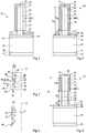
- the figure 5 is a sectional view of another embodiment of an optoelectronic device 70.
- the device 70 comprises all the elements of the optoelectronic device 30 shown in FIG. figure 2 except that the portion 32 of coarse sidewall wire 34 is extended by a portion 72 of smooth sidewall wire 74 which may have the same structure as the portion 22 of the optoelectronic device 10 shown in FIG. figure 1 .
- Portion 72 has a height H W of between 10 nm and 10 ⁇ m.
- Portion 72 is covered with an active layer 76 which may have the same structure and the same composition as the zone active 26 of the optoelectronic device 10 shown in FIG. figure 1 .
- the light radiation emitted by the active layer 76 which covers the portion 72 of the wire 20 comes from a phenomenon of electroluminescence.
- the light radiation emitted by the active zone 40 which covers the portion 32 of the wire 20 comes from a phenomenon of photoluminescence by conversion of a portion of the light radiation emitted by the active layer 76 of adjacent wires 20.
- the active zone 40 may not be continuous, that is to say not cover the rough side wall 34 completely.
- Each light-emitting diode LED of the optoelectronic device 70 can therefore emit at two different wavelengths.
- the figure 6 represents another embodiment of an optoelectronic device 80 which comprises all the elements of the device 70 except that the portion 72 of the wire 20 with smooth side wall 74 is located between the lower portion 36 and the portion 32 of the wire 20 with rough side wall 34.
- the figure 7 represents another embodiment of an optoelectronic device 90 which comprises all the elements of the device 80 represented in FIG. figure 6 with the difference that the semiconductor layer 27 and the electrode layer 28 cover the portion 72 of the smooth wall wire 74 and the portion 32 of the rough wall wire 34.
- the figure 8 represents another embodiment of an optoelectronic device 100 which comprises all the elements of the device 80 represented in FIG. figure 6 with the difference that the semiconductor layer 27 and the electrode layer 28 only cover the portion 32 of the coarse-walled wire 34 and do not cover the portion 72 of the smooth-walled wire 74.
- the figure 9 represents another embodiment of an optoelectronic device 110 which comprises all the elements of the device 70 represented in FIG. figure 5 unlike that the semiconductor layer 27 and the electrode layer 28 only cover the portion 32 of the coarse-walled wire 34 and do not cover the portion 72 of the smooth-walled wire 74.
- the embodiments shown on the figures 5 and 6 have the advantage of more efficient current injection with less leakage.
- One explanation is that the active layer is more homogeneous and the quantum boxes, which convert some of the light emitted by the active layer, emit at longer wavelengths. The spectrum emitted is then wider and more stable as a function of the voltage applied to the light-emitting diodes.
- the rough wall 34 is formed after the growth of each wire 20 by chemically etching the flanks of the wire 20.
- the possible portions of the wire 20 whose sidewalls must remain smooth, for example the portion 72 in FIG. figure 5 are then protected against etching, for example by being covered with a protective layer which is removed after the etching step.
- the yarn growth process may be a chemical vapor deposition (CVD) method or an organometallic chemical vapor deposition (MOCVD), also known as VOC (Metal Chemical Vapor Deposition).
- MOCVD Organometallic chemical vapor deposition
- VOC Metal Chemical Vapor Deposition
- MOVPE organometallic chemical vapor deposition
- MBE molecular beam epitaxy
- MBBE gas-source MBE
- MOMBE organometallic MBE
- PAMBE plasma-assisted MBE
- ALE Atomic Layer Epitaxy
- HVPE Hydride Vapor Phase Epitaxy
- electrochemical processes may be used, for example, chemical bath deposition (CBD), hydrothermal processes, liquid aerosol pyrolysis or electrodeposition.
- the process may comprise injecting into a reactor a precursor of a group III element and a precursor of a group V element.
- group III precursor elements are trimethylgallium (TMGa), triethylgallium (TEGa), trimethylindium (TMIn) or trimethylaluminum (TMAl).
- group V precursors are ammonia (NH 3 ), tertiarybutylphosphine (TBP), arsine (AsH 3 ), or asymmetric dimethylhydrazine (UDMH).
- III / V ratio The ratio between the gas flow of the precursor of the group III element and the gas flow of the precursor of the group V element.
- a precursor of an additional element is added in addition to the precursors of the III-V compound.
- the presence of the precursor of the additional element leads to the incorporation of the additional element in compound III-V to dope this compound III-V but also to the formation of a layer of a dielectric material consisting mainly of additional element and the group V element on the lateral flanks of the growing crystals of the III-V compound.
- the additional element may be silicon (Si).
- An example of a precursor of silicon is silane (SiH 4 ). This enables the N-type wires to be doped.
- the ratio of the silane flux to the trimethylgallium flux, expressed in ⁇ mol / min, is generally between 8 * 10 -5 and 2 * 10 -3 , for example about 4.10 -4 .
- the thickness of the dielectric layer of Si 3 N 4 obtained is then generally less than 10 nm.
- a method of the MOCVD type can be implemented by injection into a spray-type MOCVD reactor, a precursor gas of gallium, for example trimethylgallium (TMGa) and a nitrogen precursor gas, by for example ammonia (NH 3 ).
- a precursor gas of gallium for example trimethylgallium (TMGa)
- a nitrogen precursor gas by for example ammonia (NH 3 ).
- a carrier gas that ensures the diffusion of organometallics into the reactor is loaded organometallic in a TMGa bubbler.This is set according to standard conditions A flow of 60 sccm (standard cubic centimeters per minute) is, for example, chosen for TMGa, while a flow of 300 sccm is used for NH 3 (standard NH 3 bottle).
- the gaseous mixture further comprises the injection of silane into the silicon precursor MOCVD reactor
- the silane can be diluted in 1000 ppm hydrogen and brings a flow of 20 sccm.
- the temperature in the reactor is, for example, between 950 ° C and 1100 ° C, preferably between 990 ° C and 1060 ° C.
- a carrier gas stream for example N 2 , of 2000 sccm distributed in the two plenums is used.
- the gas flows indicated above are given as an indication and are to be adapted according to the size and specificities of the reactor.
- the rough wall 34 is obtained by placing excess hydrogen (H 2 ) in the reactor after the growth of the wires 20.
- the hydrogen is conventionally used as a carrier gas in the reactor but the inventors have shown that an excess of hydrogen can cause etching of the side walls of the son and an increase in the roughness of these walls.
- the reactor is pressurized with H 2 , for example at a pressure of 0.8 bar (80 kPa) for 5 min.
- H 2 for example at a pressure of 0.8 bar (80 kPa) for 5 min.
- the formation of asperities on the walls of the wire 20 exposed to etching is obtained.
- the rough wall 34 is obtained by partial etching of the dielectric layer covering the wire 20 and which is formed during the growth of the wire 20, so as to partially expose the wire 20.
- the etching can be carried out by placing excess hydrogen (H 2 ) in the reactor after the growth of the yarns 20.
- the exposed areas of the yarn form growth sites of the quantum dots.
- the trimethylgallium flux is interrupted while the silane stream is kept alone, for example for 5 minutes.
- the reactor is then pressurized with H 2 , for example at a pressure of 0.8 bar (80 kPa) for 5 min.
- the ratio between the silane stream and the trimethylgallium stream is increased.
- the inventors have demonstrated that the growth mechanism of the silicon nitride layer is modified when the silane is highly in excess, which leads to obtaining an irregular Si 3 N 4 layer exposing areas of the GaN wire, thus forming nucleation zones for the quantum dots. Exposed areas of the GaN wire form quantum dot growth sites.
- the ratio between the silane flux and the trimethylgallium flux expressed in ⁇ mol / min, is greater than 10 -3 .
- the silane stream is reduced so that the layer of Si 3 N 4 , which is formed on the wire, is not continuous and comprises openings which expose areas of the wire 20, these exposed areas forming growth sites quantum boxes.
- the ratio between the silane flow and the trimethylgallium flux, expressed in ⁇ mol / min, may be less than 5 * 10 -4 .
- the rough wall 34 is formed as and when the growth of each wire 20.
- the figure 10 represents another embodiment of an optoelectronic device 120 after the step of forming the wires 20 and before the step of forming the active zone 40.
- the portion 32 comprises a succession of portions 122, 124, 126 of substantially constant sections and of different diameters, each portion being connected to the next by a step 128, that is to say by a face substantially perpendicular to the axis
- the edges at the joint between the steps 128 and the portions 122, 124, 126 form growth sites of the quantum boxes.
- the steps 128 may be inclined with respect to the axis D.
- the growth parameters of the wire 20 are changed in a step between two parts 122, 124, 126 of different diameters.
- the ratio III / V passes, in a step, from an initial constant value to a final constant value, between two parts 122, 124, 126 of different diameters.
- the figure 11 represents another embodiment of an optoelectronic device 130 after the step of forming the wires 20 and before the step of forming the active zone 40.
- the portion 32 comprises a doped core 132 surrounded by a substantially undoped shell 133 comprising a succession of portions 134, 135, 136, 137 with inclined walls connected by steps 138.
- the edges at the joint between the steps 138 and 134, 135, 136, 137 parts form growth sites quantum boxes.
- the silane flow is interrupted and the flows of the gallium and nitrogen precursors are maintained.
- the temperature is decreased, for example from 1000 ° C to 750 ° C in successive stages. This causes the formation of the hull 133 from the top of the wire with successive steps 138.
- the diameter of the shell 133 decreases from the top of the wire 20.
- the figure 12 represents another embodiment of an optoelectronic device 140 after the step of forming the wires 20 and before the step of forming the active zone 40.
- the portion 32 of the wire 20 consists of an alternation of portions doped 142, for example doped GaN type N, and undoped portions 144, for example GaN.
- the undoped portions 144 have a diameter greater than the doped portions 142.
- the edges at the junctions between the undoped portions 144 and the doped portions 142 form quantum dot growth sites.
- portions 144 of GaN having diameters different than that of portions 142 of doped GaN.
- the portions 142 of doped GaN are formed with given operating parameters of the growth reactor, operating parameters of the reactor are modified to form the portions 144 of GaN.
- the pressure is modified and / or the relative composition of group III precursors and group V element precursors is modified. More specifically, a reduction of the pressure in the reactor during the formation of a portion 144 of GaN with respect to the pressure used for the formation of the portion 142 of the underlying doped GaN causes an increase in the diameter of the portion 144. of GaN with respect to the portion 142 of the underlying doped GaN.
- the figure 13 represents another embodiment of an optoelectronic device 150 after the step of forming the wires 20 and before the step of forming the active zone 40.
- each semiconductor element corresponds to a pyramid 152.
- inventors have shown that for certain growth conditions of the pyramids 152, some flanks of the pyramids are rougher than others.
- AT we have shown in figure 13 a less rough flank 154 and a more rough flank 156.
- the rougher flank asperities 156 are adapted to form quantum dot growth sites while an active layer comprising quantum wells may be formed on the less rough flank 154.
- the seed layer 19 can promote the growth of GaN with the Ga polarity.
- the ratio V / III is weak, for example less than 50. This results in the formation of pyramids comprising smooth sides and rough sides.
- the precursor streams of elements V and III can be interrupted and the growth reactor can be put under a pressure of hydrogen, for example at 0.8 bar for 10 minutes. . This causes a greater increase in the roughness of the flank 156 with respect to the flank 154.
Landscapes
- Led Devices (AREA)
Claims (10)
- Optoelektronische Vorrichtung (30) mit dreidimensionalen Halbleiterelementen (20; 152), die überwiegend aus einer ersten Verbindung hergestellt sind, die aus der Gruppe ausgewählt ist, die III-V-Verbindungen, II-VI-Verbindungen und IV-Verbindungen aufweist, wobei jedes Halbleiterelement optional mit isolierenden Teilen, die das Halbleiterelement teilweise bedecken, wenigstens eine erste Oberfläche (34) begrenzt, die zusammenhängende Facetten aufweist, die zueinander abgewinkelt sind, wobei die optoelektronische Vorrichtung Quantenpunkte (60) an wenigstens einigen der Nähte bzw. Übergänge (42) zwischen den Facetten aufweist, wobei die Quantenpunkte überwiegend aus einer Mischung der ersten Verbindung und eines zusätzlichen Elements hergestellt sind und in der Lage sind, eine erste elektromagnetische Strahlung mit einer ersten Wellenlänge zu emittieren oder zu empfangen, wobei die Vorrichtung ferner eine aktive Schicht (62; 76) aufweist, die wenigstens einen einzelnen Quantentopf oder mehrere Quantentöpfe aufweist und in der Lage ist, eine zweite elektromagnetische Strahlung mit einer zweiten Wellenlänge, die sich von der ersten Wellenlänge unterscheidet, zu emittieren oder zu empfangen, wobei die aktive Schicht die Quantenpunkte bedeckt.
- Optoelektronische Vorrichtung (30) nach Anspruch 1, wobei jedes Halbleiterelement eine zweite Oberfläche (74) aufweist, die sich von der ersten Oberfläche (34) unterscheidet, wobei die aktive Schicht (76) die zweite Oberfläche bedeckt.
- Optoelektronische Vorrichtung nach Anspruch 1 oder 2, wobei jeder Quantenpunkt (60) überwiegend aus einer InxAlyGa1-x-yN-Verbindung hergestellt ist, wobei 0≤x≤1, 0≤y≤1 und 1-x-y> 0 ist.
- Optoelektronische Vorrichtung nach einem der Ansprüche 1 bis 3, wobei die Halbleiterelemente (20) Nanodrähte, Mikrodrähte und/oder pyramidenförmige Strukturen im Nano- oder Mikrometerbereich sind.
- Optoelektronische Vorrichtung nach einem der Ansprüche 1 bis 4, wobei die Halbleiterelemente eine Form aufweisen, die entlang einer bevorzugten Richtung verlängert ist, und wobei der Abstand, gemessen senkrecht zur bevorzugten Richtung, zwischen zwei Übergängen (42) von Paaren benachbarter Übergänge größer als 5 nm ist.
- Optoelektronische Vorrichtung nach Anspruch 5, wobei der Abstand, gemessen parallel zur bevorzugten Richtung, zwischen zwei benachbarten Übergängen (42) kleiner als 1 µm ist.
- Optoelektronische Vorrichtung nach Anspruch 5, wobei die Dichte der Übergänge (42) größer als 108 Übergänge/cm2 ist.
- Verfahren zur Herstellung einer optoelektronischen Vorrichtung (30), die folgende Schritte aufweist:Ausbilden von dreidimensionalen Halbleiterelementen (20; 152), die überwiegend aus einer ersten Verbindung hergestellt sind, die aus der Gruppe ausgewählt ist, die III-V-Verbindungen, II-VI-Verbindungen und IV-Verbindungen aufweist, wobei jedes Halbleiterelement optional mit isolierenden Teilen, die das Halbleiterelement teilweise bedecken, wenigstens eine erste Oberfläche (34) begrenzt, die zusammenhängende Facetten aufweist, die zueinander abgewinkelt sind;Ausbilden von Quantenpunkten (60) an wenigstens einigen der Übergänge (42) zwischen den Facetten, wobei die Quantenpunkte überwiegend aus einer Mischung der ersten Verbindung und eines zusätzlichen Elements hergestellt sind und in der Lage sind, eine erste elektromagnetische Strahlung mit einer ersten Wellenlänge zu emittieren oder zu empfangen; undAusbilden einer aktiven Schicht (62; 76), die wenigstens einen einzelnen Quantentopf oder mehrere Quantentöpfe aufweist und in der Lage ist, eine zweite elektromagnetische Strahlung mit einer zweiten Wellenlänge, die sich von der ersten Wellenlänge unterscheidet, zu emittieren oder zu empfangen, wobei die aktive Schicht (62; 76) die Quantenpunkte (60) bedeckt.
- Verfahren nach Anspruch 8, das das Ausbilden von Halbleiterelementen (20) und das teilweise Ätzen der Halbleiterelemente zum Ausbilden der ersten Oberfläche (34) aufweist.
- Verfahren nach Anspruch 8, wobei die erste Oberfläche gleichzeitig mit dem Aufwachsen der Halbleiterelemente (20) ausgebildet wird.
Applications Claiming Priority (2)
| Application Number | Priority Date | Filing Date | Title |
|---|---|---|---|
| FR1459275A FR3026564B1 (fr) | 2014-09-30 | 2014-09-30 | Dispositif optoelectronique a elements semiconducteurs tridimensionnels |
| PCT/FR2015/052602 WO2016051078A1 (fr) | 2014-09-30 | 2015-09-29 | Dispositif optoelectronique a elements semiconducteurs tridimensionnels |
Publications (2)
| Publication Number | Publication Date |
|---|---|
| EP3201951A1 EP3201951A1 (de) | 2017-08-09 |
| EP3201951B1 true EP3201951B1 (de) | 2019-11-27 |
Family
ID=52684308
Family Applications (1)
| Application Number | Title | Priority Date | Filing Date |
|---|---|---|---|
| EP15788111.1A Active EP3201951B1 (de) | 2014-09-30 | 2015-09-29 | Optoelektronische vorrichtung mit dreidimensionalen halbleiterelementen |
Country Status (6)
| Country | Link |
|---|---|
| US (1) | US10615299B2 (de) |
| EP (1) | EP3201951B1 (de) |
| KR (1) | KR102389679B1 (de) |
| CN (1) | CN107078186B (de) |
| FR (1) | FR3026564B1 (de) |
| WO (1) | WO2016051078A1 (de) |
Families Citing this family (7)
| Publication number | Priority date | Publication date | Assignee | Title |
|---|---|---|---|---|
| FR3044470B1 (fr) * | 2015-11-30 | 2018-03-23 | Commissariat A L'energie Atomique Et Aux Energies Alternatives | Dispositif optoelectronique comportant des structures semiconductrices tridimensionnelles en configuration axiale |
| FR3076399B1 (fr) * | 2017-12-28 | 2020-01-24 | Aledia | Dispositif optoelectronique comprenant des diodes electroluminescentes tridimensionnelles |
| FR3096509B1 (fr) * | 2019-05-20 | 2021-05-28 | Aledia | Dispositif optoelectronique avec diodes electroluminescentes dont une zone dopee integre une portion externe a base d’aluminium et de nitrure de galium |
| FR3098013B1 (fr) * | 2019-06-25 | 2021-07-02 | Commissariat Energie Atomique | Procédé de fabrication d'un dispositif optoélectronique à diodes électroluminescentes de type axial |
| DE102021109960A1 (de) * | 2021-04-20 | 2022-10-20 | OSRAM Opto Semiconductors Gesellschaft mit beschränkter Haftung | Strahlungsemittierender halbleiterchip und verfahren zur herstellung eines strahlungsemittierenden halbleiterchips |
| CN114843383B (zh) * | 2022-07-01 | 2022-10-25 | 季华实验室 | Led结构及其制造方法、led显示屏 |
| CN118712294B (zh) * | 2024-08-29 | 2024-11-15 | 山东省科学院激光研究所 | 一种纳米发光二极管及其制备方法 |
Citations (1)
| Publication number | Priority date | Publication date | Assignee | Title |
|---|---|---|---|---|
| EP2333847A1 (de) * | 2008-09-01 | 2011-06-15 | Sophia School Corporation | Optische halbleiterbauelementanordnung und herstellungsverfahren dafür |
Family Cites Families (11)
| Publication number | Priority date | Publication date | Assignee | Title |
|---|---|---|---|---|
| FR1459275A (fr) | 1965-10-07 | 1966-04-29 | Lambert & Cie Soc | Perfectionnement aux installations pour le dosage des agrégats |
| US20050269286A1 (en) | 2004-06-08 | 2005-12-08 | Manish Sharma | Method of fabricating a nano-wire |
| KR100736515B1 (ko) * | 2005-12-01 | 2007-07-06 | 삼성전자주식회사 | 다공성 템플릿을 이용한 나노 와이어의 제조방법 및나노와이어 구조체 |
| WO2007097242A1 (ja) * | 2006-02-24 | 2007-08-30 | Matsushita Electric Industrial Co., Ltd. | 発光素子 |
| SE533090C2 (sv) * | 2008-07-09 | 2010-06-22 | Qunano Ab | Nanostrukturerad ljusdiod |
| CA2864212A1 (en) * | 2011-02-10 | 2012-08-16 | The Royal Institution For The Advancement Of Learning/Mcgill University | High efficiency broadband semiconductor nanowire devices and methods of fabricating without foreign metal catalysis |
| CN102280545A (zh) * | 2011-08-17 | 2011-12-14 | 中国科学院苏州纳米技术与纳米仿生研究所 | 硅基光发射器件及其制备方法 |
| US8835965B2 (en) * | 2012-01-18 | 2014-09-16 | The Penn State Research Foundation | Application of semiconductor quantum dot phosphors in nanopillar light emitting diodes |
| FR2995729B1 (fr) | 2012-09-18 | 2016-01-01 | Aledia | Dispositif opto-electrique a microfils ou nanofils semiconducteurs et son procede de fabrication |
| FR2997558B1 (fr) | 2012-10-26 | 2015-12-18 | Aledia | Dispositif opto-electrique et son procede de fabrication |
| US9166106B2 (en) * | 2012-10-26 | 2015-10-20 | Glo Ab | Nanowire sized opto-electronic structure and method for modifying selected portions of same |
-
2014
- 2014-09-30 FR FR1459275A patent/FR3026564B1/fr not_active Expired - Fee Related
-
2015
- 2015-09-29 CN CN201580053007.2A patent/CN107078186B/zh active Active
- 2015-09-29 US US15/513,797 patent/US10615299B2/en active Active
- 2015-09-29 KR KR1020177010463A patent/KR102389679B1/ko active Active
- 2015-09-29 WO PCT/FR2015/052602 patent/WO2016051078A1/fr not_active Ceased
- 2015-09-29 EP EP15788111.1A patent/EP3201951B1/de active Active
Patent Citations (1)
| Publication number | Priority date | Publication date | Assignee | Title |
|---|---|---|---|---|
| EP2333847A1 (de) * | 2008-09-01 | 2011-06-15 | Sophia School Corporation | Optische halbleiterbauelementanordnung und herstellungsverfahren dafür |
Also Published As
| Publication number | Publication date |
|---|---|
| CN107078186B (zh) | 2019-10-11 |
| FR3026564B1 (fr) | 2018-02-16 |
| US20180233610A1 (en) | 2018-08-16 |
| KR102389679B1 (ko) | 2022-04-21 |
| WO2016051078A1 (fr) | 2016-04-07 |
| FR3026564A1 (fr) | 2016-04-01 |
| US10615299B2 (en) | 2020-04-07 |
| EP3201951A1 (de) | 2017-08-09 |
| KR20170062480A (ko) | 2017-06-07 |
| CN107078186A (zh) | 2017-08-18 |
Similar Documents
| Publication | Publication Date | Title |
|---|---|---|
| EP2997598B1 (de) | Optoelektronische vorrichtung und herstellungsverfahren dafür | |
| EP2911974B1 (de) | Optoelektronische vorrichtung und herstellungsverfahren dafür | |
| EP3201951B1 (de) | Optoelektronische vorrichtung mit dreidimensionalen halbleiterelementen | |
| EP2898546B1 (de) | Optoelektronisches bauelement basierend auf halbleitermikro- oder nano-drähten, sowie dazugehöriges herstellungsverfahren | |
| EP2997605B1 (de) | Optoelektronische vorrichtung und herstellungsverfahren dafür | |
| EP3248227B1 (de) | Optoelektronisches halbleiterbauelement und herstellungsverfahren davon | |
| EP3991216B1 (de) | Verfahren zur herstellung einer optoelektronischen vorrichtung mit leuchtdioden des axialen typs | |
| FR3039004B1 (fr) | Dispositif optoelectronique a elements semiconducteurs tridimensionnels et son procede de fabrication | |
| EP3090450B1 (de) | Optoelektronische vorrichtung mit halbleiterelementen und deren herstellungsverfahren | |
| EP3014665B1 (de) | Optoelektronische vorrichtung mit verbesserter reflexion und verfahren zu ihrer herstellung | |
| EP2939276B1 (de) | Optoelektronisches bauteil mit mikrostäben oder nanostäben | |
| EP2939277B1 (de) | Optoelektronisches bauteil mit micro- oder nanostäbchen | |
| EP3224858A1 (de) | Optoelektronische vorrichtung mit dreidimensionalen halbleiterelementen und verfahren zur herstellung davon | |
| FR3000611A1 (fr) | Dispositif optoelectronique a microfils ou nanofils | |
| FR3000613A1 (fr) | Dispositif optoelectronique a microfils ou nanofils |
Legal Events
| Date | Code | Title | Description |
|---|---|---|---|
| STAA | Information on the status of an ep patent application or granted ep patent |
Free format text: STATUS: THE INTERNATIONAL PUBLICATION HAS BEEN MADE |
|
| PUAI | Public reference made under article 153(3) epc to a published international application that has entered the european phase |
Free format text: ORIGINAL CODE: 0009012 |
|
| STAA | Information on the status of an ep patent application or granted ep patent |
Free format text: STATUS: REQUEST FOR EXAMINATION WAS MADE |
|
| 17P | Request for examination filed |
Effective date: 20170323 |
|
| AK | Designated contracting states |
Kind code of ref document: A1 Designated state(s): AL AT BE BG CH CY CZ DE DK EE ES FI FR GB GR HR HU IE IS IT LI LT LU LV MC MK MT NL NO PL PT RO RS SE SI SK SM TR |
|
| AX | Request for extension of the european patent |
Extension state: BA ME |
|
| DAV | Request for validation of the european patent (deleted) | ||
| DAX | Request for extension of the european patent (deleted) | ||
| GRAP | Despatch of communication of intention to grant a patent |
Free format text: ORIGINAL CODE: EPIDOSNIGR1 |
|
| STAA | Information on the status of an ep patent application or granted ep patent |
Free format text: STATUS: GRANT OF PATENT IS INTENDED |
|
| RIC1 | Information provided on ipc code assigned before grant |
Ipc: H01L 33/06 20100101AFI20190606BHEP Ipc: H01L 33/18 20100101ALI20190606BHEP Ipc: H01L 33/24 20100101ALI20190606BHEP Ipc: H01L 33/22 20100101ALI20190606BHEP |
|
| INTG | Intention to grant announced |
Effective date: 20190628 |
|
| GRAS | Grant fee paid |
Free format text: ORIGINAL CODE: EPIDOSNIGR3 |
|
| GRAA | (expected) grant |
Free format text: ORIGINAL CODE: 0009210 |
|
| STAA | Information on the status of an ep patent application or granted ep patent |
Free format text: STATUS: THE PATENT HAS BEEN GRANTED |
|
| AK | Designated contracting states |
Kind code of ref document: B1 Designated state(s): AL AT BE BG CH CY CZ DE DK EE ES FI FR GB GR HR HU IE IS IT LI LT LU LV MC MK MT NL NO PL PT RO RS SE SI SK SM TR |
|
| REG | Reference to a national code |
Ref country code: GB Ref legal event code: FG4D Free format text: NOT ENGLISH |
|
| REG | Reference to a national code |
Ref country code: CH Ref legal event code: EP |
|
| REG | Reference to a national code |
Ref country code: AT Ref legal event code: REF Ref document number: 1207690 Country of ref document: AT Kind code of ref document: T Effective date: 20191215 |
|
| REG | Reference to a national code |
Ref country code: DE Ref legal event code: R096 Ref document number: 602015042590 Country of ref document: DE |
|
| REG | Reference to a national code |
Ref country code: IE Ref legal event code: FG4D Free format text: LANGUAGE OF EP DOCUMENT: FRENCH |
|
| REG | Reference to a national code |
Ref country code: NL Ref legal event code: MP Effective date: 20191127 |
|
| REG | Reference to a national code |
Ref country code: LT Ref legal event code: MG4D |
|
| PG25 | Lapsed in a contracting state [announced via postgrant information from national office to epo] |
Ref country code: SE Free format text: LAPSE BECAUSE OF FAILURE TO SUBMIT A TRANSLATION OF THE DESCRIPTION OR TO PAY THE FEE WITHIN THE PRESCRIBED TIME-LIMIT Effective date: 20191127 Ref country code: NL Free format text: LAPSE BECAUSE OF FAILURE TO SUBMIT A TRANSLATION OF THE DESCRIPTION OR TO PAY THE FEE WITHIN THE PRESCRIBED TIME-LIMIT Effective date: 20191127 Ref country code: LT Free format text: LAPSE BECAUSE OF FAILURE TO SUBMIT A TRANSLATION OF THE DESCRIPTION OR TO PAY THE FEE WITHIN THE PRESCRIBED TIME-LIMIT Effective date: 20191127 Ref country code: GR Free format text: LAPSE BECAUSE OF FAILURE TO SUBMIT A TRANSLATION OF THE DESCRIPTION OR TO PAY THE FEE WITHIN THE PRESCRIBED TIME-LIMIT Effective date: 20200228 Ref country code: BG Free format text: LAPSE BECAUSE OF FAILURE TO SUBMIT A TRANSLATION OF THE DESCRIPTION OR TO PAY THE FEE WITHIN THE PRESCRIBED TIME-LIMIT Effective date: 20200227 Ref country code: NO Free format text: LAPSE BECAUSE OF FAILURE TO SUBMIT A TRANSLATION OF THE DESCRIPTION OR TO PAY THE FEE WITHIN THE PRESCRIBED TIME-LIMIT Effective date: 20200227 Ref country code: FI Free format text: LAPSE BECAUSE OF FAILURE TO SUBMIT A TRANSLATION OF THE DESCRIPTION OR TO PAY THE FEE WITHIN THE PRESCRIBED TIME-LIMIT Effective date: 20191127 Ref country code: LV Free format text: LAPSE BECAUSE OF FAILURE TO SUBMIT A TRANSLATION OF THE DESCRIPTION OR TO PAY THE FEE WITHIN THE PRESCRIBED TIME-LIMIT Effective date: 20191127 |
|
| PG25 | Lapsed in a contracting state [announced via postgrant information from national office to epo] |
Ref country code: HR Free format text: LAPSE BECAUSE OF FAILURE TO SUBMIT A TRANSLATION OF THE DESCRIPTION OR TO PAY THE FEE WITHIN THE PRESCRIBED TIME-LIMIT Effective date: 20191127 Ref country code: IS Free format text: LAPSE BECAUSE OF FAILURE TO SUBMIT A TRANSLATION OF THE DESCRIPTION OR TO PAY THE FEE WITHIN THE PRESCRIBED TIME-LIMIT Effective date: 20200327 Ref country code: RS Free format text: LAPSE BECAUSE OF FAILURE TO SUBMIT A TRANSLATION OF THE DESCRIPTION OR TO PAY THE FEE WITHIN THE PRESCRIBED TIME-LIMIT Effective date: 20191127 |
|
| PG25 | Lapsed in a contracting state [announced via postgrant information from national office to epo] |
Ref country code: AL Free format text: LAPSE BECAUSE OF FAILURE TO SUBMIT A TRANSLATION OF THE DESCRIPTION OR TO PAY THE FEE WITHIN THE PRESCRIBED TIME-LIMIT Effective date: 20191127 |
|
| PG25 | Lapsed in a contracting state [announced via postgrant information from national office to epo] |
Ref country code: CZ Free format text: LAPSE BECAUSE OF FAILURE TO SUBMIT A TRANSLATION OF THE DESCRIPTION OR TO PAY THE FEE WITHIN THE PRESCRIBED TIME-LIMIT Effective date: 20191127 Ref country code: RO Free format text: LAPSE BECAUSE OF FAILURE TO SUBMIT A TRANSLATION OF THE DESCRIPTION OR TO PAY THE FEE WITHIN THE PRESCRIBED TIME-LIMIT Effective date: 20191127 Ref country code: PT Free format text: LAPSE BECAUSE OF FAILURE TO SUBMIT A TRANSLATION OF THE DESCRIPTION OR TO PAY THE FEE WITHIN THE PRESCRIBED TIME-LIMIT Effective date: 20200419 Ref country code: EE Free format text: LAPSE BECAUSE OF FAILURE TO SUBMIT A TRANSLATION OF THE DESCRIPTION OR TO PAY THE FEE WITHIN THE PRESCRIBED TIME-LIMIT Effective date: 20191127 Ref country code: DK Free format text: LAPSE BECAUSE OF FAILURE TO SUBMIT A TRANSLATION OF THE DESCRIPTION OR TO PAY THE FEE WITHIN THE PRESCRIBED TIME-LIMIT Effective date: 20191127 Ref country code: ES Free format text: LAPSE BECAUSE OF FAILURE TO SUBMIT A TRANSLATION OF THE DESCRIPTION OR TO PAY THE FEE WITHIN THE PRESCRIBED TIME-LIMIT Effective date: 20191127 |
|
| REG | Reference to a national code |
Ref country code: DE Ref legal event code: R097 Ref document number: 602015042590 Country of ref document: DE |
|
| PG25 | Lapsed in a contracting state [announced via postgrant information from national office to epo] |
Ref country code: SK Free format text: LAPSE BECAUSE OF FAILURE TO SUBMIT A TRANSLATION OF THE DESCRIPTION OR TO PAY THE FEE WITHIN THE PRESCRIBED TIME-LIMIT Effective date: 20191127 Ref country code: SM Free format text: LAPSE BECAUSE OF FAILURE TO SUBMIT A TRANSLATION OF THE DESCRIPTION OR TO PAY THE FEE WITHIN THE PRESCRIBED TIME-LIMIT Effective date: 20191127 |
|
| REG | Reference to a national code |
Ref country code: AT Ref legal event code: MK05 Ref document number: 1207690 Country of ref document: AT Kind code of ref document: T Effective date: 20191127 |
|
| PLBE | No opposition filed within time limit |
Free format text: ORIGINAL CODE: 0009261 |
|
| STAA | Information on the status of an ep patent application or granted ep patent |
Free format text: STATUS: NO OPPOSITION FILED WITHIN TIME LIMIT |
|
| 26N | No opposition filed |
Effective date: 20200828 |
|
| PG25 | Lapsed in a contracting state [announced via postgrant information from national office to epo] |
Ref country code: AT Free format text: LAPSE BECAUSE OF FAILURE TO SUBMIT A TRANSLATION OF THE DESCRIPTION OR TO PAY THE FEE WITHIN THE PRESCRIBED TIME-LIMIT Effective date: 20191127 Ref country code: SI Free format text: LAPSE BECAUSE OF FAILURE TO SUBMIT A TRANSLATION OF THE DESCRIPTION OR TO PAY THE FEE WITHIN THE PRESCRIBED TIME-LIMIT Effective date: 20191127 Ref country code: PL Free format text: LAPSE BECAUSE OF FAILURE TO SUBMIT A TRANSLATION OF THE DESCRIPTION OR TO PAY THE FEE WITHIN THE PRESCRIBED TIME-LIMIT Effective date: 20191127 |
|
| PG25 | Lapsed in a contracting state [announced via postgrant information from national office to epo] |
Ref country code: IT Free format text: LAPSE BECAUSE OF FAILURE TO SUBMIT A TRANSLATION OF THE DESCRIPTION OR TO PAY THE FEE WITHIN THE PRESCRIBED TIME-LIMIT Effective date: 20191127 |
|
| REG | Reference to a national code |
Ref country code: CH Ref legal event code: PL |
|
| REG | Reference to a national code |
Ref country code: BE Ref legal event code: MM Effective date: 20200930 |
|
| PG25 | Lapsed in a contracting state [announced via postgrant information from national office to epo] |
Ref country code: LU Free format text: LAPSE BECAUSE OF NON-PAYMENT OF DUE FEES Effective date: 20200929 |
|
| PG25 | Lapsed in a contracting state [announced via postgrant information from national office to epo] |
Ref country code: LI Free format text: LAPSE BECAUSE OF NON-PAYMENT OF DUE FEES Effective date: 20200930 Ref country code: IE Free format text: LAPSE BECAUSE OF NON-PAYMENT OF DUE FEES Effective date: 20200929 Ref country code: CH Free format text: LAPSE BECAUSE OF NON-PAYMENT OF DUE FEES Effective date: 20200930 Ref country code: BE Free format text: LAPSE BECAUSE OF NON-PAYMENT OF DUE FEES Effective date: 20200930 |
|
| PG25 | Lapsed in a contracting state [announced via postgrant information from national office to epo] |
Ref country code: TR Free format text: LAPSE BECAUSE OF FAILURE TO SUBMIT A TRANSLATION OF THE DESCRIPTION OR TO PAY THE FEE WITHIN THE PRESCRIBED TIME-LIMIT Effective date: 20191127 Ref country code: MT Free format text: LAPSE BECAUSE OF FAILURE TO SUBMIT A TRANSLATION OF THE DESCRIPTION OR TO PAY THE FEE WITHIN THE PRESCRIBED TIME-LIMIT Effective date: 20191127 Ref country code: CY Free format text: LAPSE BECAUSE OF FAILURE TO SUBMIT A TRANSLATION OF THE DESCRIPTION OR TO PAY THE FEE WITHIN THE PRESCRIBED TIME-LIMIT Effective date: 20191127 |
|
| PG25 | Lapsed in a contracting state [announced via postgrant information from national office to epo] |
Ref country code: MK Free format text: LAPSE BECAUSE OF FAILURE TO SUBMIT A TRANSLATION OF THE DESCRIPTION OR TO PAY THE FEE WITHIN THE PRESCRIBED TIME-LIMIT Effective date: 20191127 Ref country code: MC Free format text: LAPSE BECAUSE OF FAILURE TO SUBMIT A TRANSLATION OF THE DESCRIPTION OR TO PAY THE FEE WITHIN THE PRESCRIBED TIME-LIMIT Effective date: 20191127 |
|
| REG | Reference to a national code |
Ref country code: DE Ref legal event code: R079 Ref document number: 602015042590 Country of ref document: DE Free format text: PREVIOUS MAIN CLASS: H01L0033060000 Ipc: H10H0020812000 |
|
| PGFP | Annual fee paid to national office [announced via postgrant information from national office to epo] |
Ref country code: DE Payment date: 20250919 Year of fee payment: 11 |
|
| PGFP | Annual fee paid to national office [announced via postgrant information from national office to epo] |
Ref country code: GB Payment date: 20250923 Year of fee payment: 11 |
|
| PGFP | Annual fee paid to national office [announced via postgrant information from national office to epo] |
Ref country code: FR Payment date: 20250924 Year of fee payment: 11 |