EP3202032B1 - Separateur de frequence pour signaux rf pour un amplificateur de puissance e/f2 de classe à large bande 60 ghz - Google Patents
Separateur de frequence pour signaux rf pour un amplificateur de puissance e/f2 de classe à large bande 60 ghz Download PDFInfo
- Publication number
- EP3202032B1 EP3202032B1 EP15847423.9A EP15847423A EP3202032B1 EP 3202032 B1 EP3202032 B1 EP 3202032B1 EP 15847423 A EP15847423 A EP 15847423A EP 3202032 B1 EP3202032 B1 EP 3202032B1
- Authority
- EP
- European Patent Office
- Prior art keywords
- port
- secondary winding
- signal
- electrical connection
- connection
- Prior art date
- Legal status (The legal status is an assumption and is not a legal conclusion. Google has not performed a legal analysis and makes no representation as to the accuracy of the status listed.)
- Active
Links
Images




Classifications
-
- H—ELECTRICITY
- H03—ELECTRONIC CIRCUITRY
- H03H—IMPEDANCE NETWORKS, e.g. RESONANT CIRCUITS; RESONATORS
- H03H7/00—Multiple-port networks comprising only passive electrical elements as network components
- H03H7/38—Impedance-matching networks
-
- H—ELECTRICITY
- H01—ELECTRIC ELEMENTS
- H01F—MAGNETS; INDUCTANCES; TRANSFORMERS; SELECTION OF MATERIALS FOR THEIR MAGNETIC PROPERTIES
- H01F27/00—Details of transformers or inductances, in general
- H01F27/28—Coils; Windings; Conductive connections
- H01F27/2823—Wires
-
- H—ELECTRICITY
- H01—ELECTRIC ELEMENTS
- H01F—MAGNETS; INDUCTANCES; TRANSFORMERS; SELECTION OF MATERIALS FOR THEIR MAGNETIC PROPERTIES
- H01F27/00—Details of transformers or inductances, in general
- H01F27/28—Coils; Windings; Conductive connections
- H01F27/29—Terminals; Tapping arrangements for signal inductances
-
- H—ELECTRICITY
- H01—ELECTRIC ELEMENTS
- H01Q—ANTENNAS, i.e. RADIO AERIALS
- H01Q1/00—Details of, or arrangements associated with, antennas
- H01Q1/50—Structural association of antennas with earthing switches, lead-in devices or lightning protectors
-
- H—ELECTRICITY
- H03—ELECTRONIC CIRCUITRY
- H03F—AMPLIFIERS
- H03F1/00—Details of amplifiers with only discharge tubes, only semiconductor devices or only unspecified devices as amplifying elements
- H03F1/02—Modifications of amplifiers to raise the efficiency, e.g. gliding Class A stages, use of an auxiliary oscillation
- H03F1/0205—Modifications of amplifiers to raise the efficiency, e.g. gliding Class A stages, use of an auxiliary oscillation in transistor amplifiers
-
- H—ELECTRICITY
- H03—ELECTRONIC CIRCUITRY
- H03F—AMPLIFIERS
- H03F1/00—Details of amplifiers with only discharge tubes, only semiconductor devices or only unspecified devices as amplifying elements
- H03F1/56—Modifications of input or output impedances, not otherwise provided for
- H03F1/565—Modifications of input or output impedances, not otherwise provided for using inductive elements
-
- H—ELECTRICITY
- H03—ELECTRONIC CIRCUITRY
- H03F—AMPLIFIERS
- H03F3/00—Amplifiers with only discharge tubes or only semiconductor devices as amplifying elements
- H03F3/189—High-frequency amplifiers, e.g. radio frequency amplifiers
- H03F3/19—High-frequency amplifiers, e.g. radio frequency amplifiers with semiconductor devices only
- H03F3/193—High-frequency amplifiers, e.g. radio frequency amplifiers with semiconductor devices only with field-effect devices
-
- H—ELECTRICITY
- H03—ELECTRONIC CIRCUITRY
- H03F—AMPLIFIERS
- H03F3/00—Amplifiers with only discharge tubes or only semiconductor devices as amplifying elements
- H03F3/20—Power amplifiers, e.g. Class B amplifiers, Class C amplifiers
- H03F3/21—Power amplifiers, e.g. Class B amplifiers, Class C amplifiers with semiconductor devices only
- H03F3/211—Power amplifiers, e.g. Class B amplifiers, Class C amplifiers with semiconductor devices only using a combination of several amplifiers
-
- H—ELECTRICITY
- H03—ELECTRONIC CIRCUITRY
- H03F—AMPLIFIERS
- H03F3/00—Amplifiers with only discharge tubes or only semiconductor devices as amplifying elements
- H03F3/20—Power amplifiers, e.g. Class B amplifiers, Class C amplifiers
- H03F3/21—Power amplifiers, e.g. Class B amplifiers, Class C amplifiers with semiconductor devices only
- H03F3/217—Class D power amplifiers; Switching amplifiers
- H03F3/2171—Class D power amplifiers; Switching amplifiers with field-effect devices
-
- H—ELECTRICITY
- H03—ELECTRONIC CIRCUITRY
- H03F—AMPLIFIERS
- H03F3/00—Amplifiers with only discharge tubes or only semiconductor devices as amplifying elements
- H03F3/20—Power amplifiers, e.g. Class B amplifiers, Class C amplifiers
- H03F3/21—Power amplifiers, e.g. Class B amplifiers, Class C amplifiers with semiconductor devices only
- H03F3/217—Class D power amplifiers; Switching amplifiers
- H03F3/2176—Class E amplifiers
-
- H—ELECTRICITY
- H03—ELECTRONIC CIRCUITRY
- H03F—AMPLIFIERS
- H03F3/00—Amplifiers with only discharge tubes or only semiconductor devices as amplifying elements
- H03F3/20—Power amplifiers, e.g. Class B amplifiers, Class C amplifiers
- H03F3/24—Power amplifiers, e.g. Class B amplifiers, Class C amplifiers of transmitter output stages
- H03F3/245—Power amplifiers, e.g. Class B amplifiers, Class C amplifiers of transmitter output stages with semiconductor devices only
-
- H—ELECTRICITY
- H03—ELECTRONIC CIRCUITRY
- H03H—IMPEDANCE NETWORKS, e.g. RESONANT CIRCUITS; RESONATORS
- H03H7/00—Multiple-port networks comprising only passive electrical elements as network components
- H03H7/01—Frequency selective two-port networks
- H03H7/09—Filters comprising mutual inductance
-
- H—ELECTRICITY
- H03—ELECTRONIC CIRCUITRY
- H03H—IMPEDANCE NETWORKS, e.g. RESONANT CIRCUITS; RESONATORS
- H03H7/00—Multiple-port networks comprising only passive electrical elements as network components
- H03H7/38—Impedance-matching networks
- H03H7/40—Automatic matching of load impedance to source impedance
-
- H—ELECTRICITY
- H03—ELECTRONIC CIRCUITRY
- H03H—IMPEDANCE NETWORKS, e.g. RESONANT CIRCUITS; RESONATORS
- H03H7/00—Multiple-port networks comprising only passive electrical elements as network components
- H03H7/42—Networks for transforming balanced signals into unbalanced signals and vice versa, e.g. baluns
- H03H7/425—Balance-balance networks
-
- H—ELECTRICITY
- H03—ELECTRONIC CIRCUITRY
- H03H—IMPEDANCE NETWORKS, e.g. RESONANT CIRCUITS; RESONATORS
- H03H7/00—Multiple-port networks comprising only passive electrical elements as network components
- H03H7/48—Networks for connecting several sources or loads, working on the same frequency or frequency band, to a common load or source
-
- H—ELECTRICITY
- H03—ELECTRONIC CIRCUITRY
- H03F—AMPLIFIERS
- H03F2200/00—Indexing scheme relating to amplifiers
- H03F2200/318—A matching circuit being used as coupling element between two amplifying stages
-
- H—ELECTRICITY
- H03—ELECTRONIC CIRCUITRY
- H03F—AMPLIFIERS
- H03F2200/00—Indexing scheme relating to amplifiers
- H03F2200/451—Indexing scheme relating to amplifiers the amplifier being a radio frequency amplifier
-
- H—ELECTRICITY
- H03—ELECTRONIC CIRCUITRY
- H03F—AMPLIFIERS
- H03F2200/00—Indexing scheme relating to amplifiers
- H03F2200/534—Transformer coupled at the input of an amplifier
-
- H—ELECTRICITY
- H03—ELECTRONIC CIRCUITRY
- H03F—AMPLIFIERS
- H03F2200/00—Indexing scheme relating to amplifiers
- H03F2200/537—A transformer being used as coupling element between two amplifying stages
-
- H—ELECTRICITY
- H03—ELECTRONIC CIRCUITRY
- H03F—AMPLIFIERS
- H03F2200/00—Indexing scheme relating to amplifiers
- H03F2200/541—Transformer coupled at the output of an amplifier
-
- H—ELECTRICITY
- H03—ELECTRONIC CIRCUITRY
- H03F—AMPLIFIERS
- H03F2203/00—Indexing scheme relating to amplifiers with only discharge tubes or only semiconductor devices as amplifying elements covered by H03F3/00
- H03F2203/20—Indexing scheme relating to power amplifiers, e.g. Class B amplifiers, Class C amplifiers
- H03F2203/21—Indexing scheme relating to power amplifiers, e.g. Class B amplifiers, Class C amplifiers with semiconductor devices only
- H03F2203/211—Indexing scheme relating to power amplifiers, e.g. Class B amplifiers, Class C amplifiers with semiconductor devices only using a combination of several amplifiers
- H03F2203/21106—An input signal being distributed in parallel over the inputs of a plurality of power amplifiers
-
- H—ELECTRICITY
- H03—ELECTRONIC CIRCUITRY
- H03F—AMPLIFIERS
- H03F2203/00—Indexing scheme relating to amplifiers with only discharge tubes or only semiconductor devices as amplifying elements covered by H03F3/00
- H03F2203/20—Indexing scheme relating to power amplifiers, e.g. Class B amplifiers, Class C amplifiers
- H03F2203/21—Indexing scheme relating to power amplifiers, e.g. Class B amplifiers, Class C amplifiers with semiconductor devices only
- H03F2203/211—Indexing scheme relating to power amplifiers, e.g. Class B amplifiers, Class C amplifiers with semiconductor devices only using a combination of several amplifiers
- H03F2203/21139—An impedance adaptation circuit being added at the output of a power amplifier stage
-
- H—ELECTRICITY
- H03—ELECTRONIC CIRCUITRY
- H03H—IMPEDANCE NETWORKS, e.g. RESONANT CIRCUITS; RESONATORS
- H03H7/00—Multiple-port networks comprising only passive electrical elements as network components
- H03H7/42—Networks for transforming balanced signals into unbalanced signals and vice versa, e.g. baluns
- H03H7/425—Balance-balance networks
- H03H7/427—Common-mode filters
Definitions
- the present invention relates generally to an RF splitter for amplifier circuits and in particular for a 60GHz wideband class E/F 2 power amplifier.
- Radio frequency (RF) power amplifier is a key component of radios that functions to convert a low power RF signal into a larger signal having significant power for driving, for example, the antenna of a transmitter.
- RF Radio frequency
- CMOS radios a key technical challenge of 60 GHz CMOS radios is poor efficiency of their power amplifier (PA).
- PA power amplifier
- a nonlinear switch-mode PA can be used to improve the total system efficiency.
- Switching power amplifiers are rarely seen at mm-wave frequencies due to the large output capacitance and low current capability of CMOS transistors.
- a two-turn inductor is exploited to realize a switch-mode PA at 60 GHz. This inductor, however, must be large enough to simultaneously satisfy the required reactance for both fundamental and second harmonics. Consequently, its relatively large inductance limits the output transistor size so the PA output power (Pout) is less than 10 dBm.
- JP-2010/183167 provides a power distribution circuit of a small area and/or low loss.
- the power distribution circuit has a primary side coil 221 for generating a magnetic flux by inputting an alternating current signal to an input terminal, a first secondary side coil 231 connected between a first output terminal and a second output terminal to generate a first alternating current signal by the magnetic flux generated by the primary side coil, and a second secondary side coil 232 connected between a third output terminal and a fourth output terminal to generate a second alternating current signal by the magnetic flux generated by the primary side coil, wherein the first secondary side coil 231 and the second secondary side coil 232 output two sets of differential signals from the first output terminal, the second output terminal, the third output terminal and the fourth output terminal.
- US-2005/242916 provides an apparatus and method for reducing common mode noise capacitive coupling from a primary winding to a secondary winding in a transformer.
- the primary winding has two terminals and a plurality of coil turns therebetween formed by a plurality of PCB layers sandwiched together, each having at least one of the coil turns formed thereon.
- the coils turns on each PCB layer are connected in a predetermined way to form the primary winding.
- Each terminal of the primary winding is connected to a coil turn on a separate corresponding PCB layer.
- the PCB layers are stacked layers to form the primary winding.
- the secondary winding or windings are positioned adjacent to a selected one of the stacked PCB layers that is in a position in the stack substantially midway between the first and second PCB layers.; Preferably, the PCB layer closest to the secondary winding is comprised of only one coil turn so as to further minimize the common mode noise.
- the transformer windings are positioned in a secondary-primary-secondary arrangement wherein two halves of the primary winding are combined into one PCB winding.
- the present invention may be used for a planar matrix transformer.
- US-2014/125126 provides a transformer (2A) outputs differential signals of a positive phase signal (Vout2Ap) having phase ⁇ 1+90° and a negative phase signal (Vout2An) having phase ⁇ 1-90°.
- a transformer (2B) outputs differential signals of a positive phase signal (Vout2Bp) having phase ⁇ 2+90° and a negative phase signal (Vout2Bn) having phase ⁇ 2-90°.
- An adding circuit (3) composes a pair of differential output signals, as signals corrected in phase error ( ⁇ 1- ⁇ 2) generated in the transformers (2A, 2B), in a manner of summing up vectors of two pairs of the differential signals outputted from the transformers (2A, 2B) for the positive phase signal and the negative phase signal, respectively.
- the present invention provides a radio frequency (RF) signal splitter in line with claim 1 and a corresponding method in line with claim 7.
- RF radio frequency
- the PA utilizes a proper second-harmonic termination in the last stage and low/moderate magnetic coupling factor transformers in the intermediate stages to reach the best product of power added efficiency (PAE) and bandwidth.
- the PA is also stabilized against the combination of DM and CM oscillation modes.
- the invention also provides a technique to stabilize transformer-based mm-wave amplifiers against various modes of undesired oscillations.
- the power amplifier has been fabricated in standard digital 40 nm CMOS having 17.9 dBm P sat .
- the PA can be incorporated within a wide range of applications including, for example, mobile devices.
- FIG. 1 A high level schematic of an example class-E/F power amplifier is shown in Figure 1 .
- the circuit generally referenced 10, comprises an input matching network 12, switch transistor M 1 (modeled as equivalent circuit 16, capacitor C s - C out , inductor L s and matching network 14 connected to the antenna load R L .
- R on and C out are the on-state channel resistance and off-state output capacitance of transistor M 1 , respectively.
- R on ⁇ C out is invariant to changes in the width of transistor M 1 .
- I DC and I rms are defined as the average and RMS values of M 1 drain current, and C S is the PA desired shunt capacitance to satisfy the ZVS criterion.
- V sat represents the transistor's average V DS in the on-state.
- C S limits the width of the transistor at mm-wave, which leads to a dramatic increase in R on and thus V sat of the switching device.
- Table 1 Waveform Parameters E E/F 2 E/F 3 E/F 2,3 E/F 4 E/F 2,4 F C 3.14 1.13 3.14 2.31 2.45 0.97 F I 1.54 1.48 1.52 1.47 1.55 1.46 F PI 2.86 3.33 3.06 2.67 3.27 3.6
- Table 2 Technology Parameters R in C in R on C out I out 27k ⁇ / ⁇ m 1fF/ ⁇ m 850 ⁇ / ⁇ m 0.6fF/ ⁇ m 0.55mA/ ⁇ m
- the transistor cut-off frequency f max should be at least three to four times higher than f 0 .
- f m ⁇ 2 ⁇ I out ⁇ C out ⁇ 1 F C F PI V DD ⁇ F I 2 R on I out ⁇
- the f m can be increased by migrating to a more advanced technology or by using a matching network with lower F PI and F C .
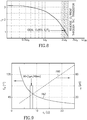
- Figure 2 predicts f m for different flavors of class-E/F PA by utilizing Equation 8 and waveform and technology parameters of Tables 1 and 2.
- Figure 2 indicates f m can be extended to 60 GHz in 40 nm CMOS for class-E/F 2 operation when the effective load of the transistor is realized as an open circuit at the second harmonic 2 ⁇ 0 .
- Power Amplifier A high level schematic diagram illustrating an example power amplifier is shown in Figure 3 .
- the circuit generally referenced 20, comprises several sections including an input power splitter 30, pre-driver amplifier stage 32, low k m transformer (TRX) 34, driver amplifier stage 36, cross-connect splitter of the present invention 38, output amplifier stage 40, series combiner 42 and parallel combiner 44.
- TRX low k m transformer
- the PA 20 incorporates a three stage common-source pseudo-differential pair to compensate for the gain penalty G p of the class-E/F 2 operation in the last PA stage 40.
- a transformer-based power splitter 22 converts the singled-ended S in input 48 to two differential signals feeding pre-drivers 24. Another set of splitters 28 is added before the four parallel units of the output stage.
- a combination of series-parallel combining is used in the output matching network to generate the output signal S out 50.
- Two-way differential series combining 42 is achieved using a distributed active transformer 46 to reduce the resistive load seen by each transistor such that the systematic P out reduction of class-E/F 2 is partially compensated.
- the output devices can be smaller for the same P out , which effectively improves the transistors' internal loss and f max . Hence, they can generate a stronger 2 nd harmonic current, which is beneficial for the class-E/F 2 operation.
- Circuit block 122 includes an ideal transformer (TRX) 124 and resonates at the fundamental frequency ⁇ 0 .
- TRX transformer
- a graph illustrating matching network efficiency versus frequency is shown in Figure 5 .
- the total effective inductance at the output of the matching network (4L s3 +L asn +L asp )/2 must resonate with the parasitic capacitance of the pad (C L ) to optimize its insertion loss.
- FIG. 6 A high level schematic diagram illustrating an equivalent half-circuit model of the output matching network for common mode (CM) is shown in Figure 6 . It is important to note that the behavior of the impedance matching network is entirely different for common-mode (CM) input signals compared with that for DM signals.
- FIG 7 A diagram illustrating the current flow in the primary 156 and secondary 154 of the output matching network transformer 152 for CM signals is shown in Figure 7 .
- the transformer coupling factor k m is negligible in CM excitation and thus R L , C L and L s3 cannot be seen by even harmonics.
- the transmission line and transformer primary inductance which is seen by CM signals, has to resonate with Cs at the second harmonic 2 ⁇ 0 to satisfy class-E/F 2 operation.
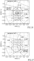
- FIG. 9 A graph illustrating the required L S and C S for class-E/F operation versus resistive load seen by the switch transistor is shown in Figure 9 .
- the graph shows the optimum required class-E/F 2 PA shunt capacitance C S and series inductance L S at fundamental frequency versus the load resistance presented by the matching network.
- the matching network geometry design is initiated by choosing the switch transistor dimension such that its output capacitor absorbs the entire C S .
- C S also depends on L S and the load resistance presented by the matching network, as can be gathered from Figure 9 . Hence, several iterations are needed to find the optimal size combination of the transistor, transformer and matching network. This procedure results in an optimal unit power transistor size of 96 (1 ⁇ m/40nm) with 1.3 dB insertion loss of the output matching network. Note that the class-E/F 2 optimal combination is different from the goal of maximizing the output power or gain.
- two transistor based power splitters along with additional series inductance and a differential strip-line are respectively added at the input of the pre-driver 32 and driver 36 stages to feed differential pairs and provide their required source reactance.
- FIG. 10 A schematic diagram illustrating the half-circuit of the PA pseudo-differential stage is shown in Figure 10 .
- Each pseudo-differential pair along with their parasitic capacitance C gd and matching networks can potentially act as two coupled Pierce oscillators and create CM instability. It can be shown that its resonant frequency is very close to the operating frequency ( ⁇ 0.7-0.8 ⁇ 0 ) such that neither (1) adding an RC stabilization network at the MOS gate nor (2) matching network loss can dampen the oscillation without affecting the precious power gain at ⁇ 0 .
- R B ⁇ 3 k ⁇ resistors between the center tap of the secondary windings of the input and inter-stage transformers and gate bias voltage can cancel out the CM currents at the transformer secondary winding. Hence, any CM oscillation will be dampened.
- a combination of CM and differential mode (DM) oscillation can potentially happen in the transformer splitter, i.e. cross-connect splitter 28 ( Figure 3 ).
- FIG. 11 A schematic diagram illustrating an example cross-connect transformer splitter of the present invention is shown in Figure 11 .
- the well-known neutralization technique can be used to improve DM stability and gain sensitivity to the load impedance.
- the PA is stabilized for CM oscillation by use of relatively large resistors (e.g., R B ⁇ 3k ⁇ ) between the center tap of the secondary windings of the transformers and gate bias voltage.
- resistors e.g., R B ⁇ 3k ⁇
- a parallel RC network e.g., 51 ⁇
- each differential pair 181, 183 coupled to the transformer splitter 182 could oscillate in CM but with 180°phase shift to each other. Hence, neither neutralization capacitors nor R B will damp this oscillation.
- the present invention provides a solution by adding a relatively weak cross connection 188 between the splitter's in-phase ports to reduce the loop gain of this oscillation mode without affecting the splitter's main function.
- a lossy path is added between the ground connections of two pseudo-differential pairs across the splitter.
- the width of the added cross connection is preferably at least four times narrower than the main metal line of the splitter.
- the effective Q-factor of the PA input/output matching network is degraded by the 50 ⁇ load and RF pad parasitic capacitance, CL ⁇ 50 fF, to about 1 to 2 at 60 GHz, thus making these networks wideband.
- the impedance seen at the input of the transformer network (r in +jX in in Figure 12 ) changes significantly over frequency and thus limits the bandwidth of the PA.
- Figure 13 illustrates the position of zeros and poles of the X in transfer function.
- the mm-wave power amplifier has been fabricated in an integrated circuit using 40nm 1.1V CMOS technology.
- a layout diagram illustrating a top view of the splitter portion of the present invention is shown in Figure 15A .
- a layout diagram illustrating a bottom view of the splitter portion of the present invention is shown in Figure 15B .
- the circuit, generally referenced 260 comprises the primary winding 262 of the splitter, first secondary winding 266, second secondary winding 264, a connection 270 connecting the positive polarity ports of the secondary windings 264, 266, a connection 268 connecting the negative polarity ports of the secondary windings 264, 266 and V DD trace 274.
- the transformers comprising the PA are completely filled with dummy metal strips to comply with the strict metal density rules.
- the amount of the metal fills right underneath the transformer windings is kept at minimum to reduce the extra parasitic capacitance and eddy current losses. Electromagnetic simulations, however, reveal an additional loss of 0.2 to 0.4 dB for each matching network.
- the PA achieves a peak power gain of 21.6 dB at 58 GHz with a 3dB bandwidth of 9.7 GHz (i.e. 51.5 to 61.2 GHz).
- the S 11 , S 22 and S 12 are respectively better than - 6, -7 and -42 dB within 50 to 67 GHz.
- the large-signal measurements were performed by a mixed-signal active load-pull setup. Consuming ⁇ 0.3 A from a 1 V supply, the measured P 1dB and P sat are respectively 14.9 dBm and 17.9 dBm with 20.5% PAE max at 60 GHz.
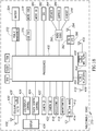
- FIG. 18 A block diagram illustrating an example tablet/mobile device incorporating the power amplifier is shown in Figure 18 .
- the mobile device is preferably a two-way communication device having voice and/or data communication capabilities.
- the device optionally has the capability to communicate with other computer systems via the Internet.
- the mobile device may comprise any suitable wired or wireless device such as multimedia player, mobile communication device, digital still or video camera, cellular phone, smartphone, iPhone, PDA, PNA, Bluetooth device, tablet computing device such as the iPad or other iOS device, Android device, Surface, Nexus, Google Glass, etc.
- the device is shown as a mobile device, such as a cellular based telephone, smartphone or superphone. Note that this example is not intended to limit the scope of the mechanism as the invention can be implemented in a wide variety of communication devices. It is further appreciated the mobile device shown is intentionally simplified to illustrate only certain components, as the mobile device may comprise other components and subsystems beyond those shown.
- the mobile device comprises one or more processors 400 which may comprise a baseband processor, CPU, microprocessor, DSP, etc., optionally having both analog and digital portions.
- the mobile device may comprise a plurality of cellular radios 430 and associated antennas 432. Radios for the basic cellular link and any number of other wireless standards and Radio Access Technologies (RATs) may be included.
- RATs Radio Access Technologies
- Examples include, but are not limited to, Third Generation (3G) Long Term Evolution (LTE), Code Division Multiple Access (CDMA), Personal Communication Services (PCS), Global System for Mobile Communication (GSM)/GPRS/EDGE 3G; WCDMA; WiMAX for providing WiMAX wireless connectivity when within the range of a WiMAX wireless network; Bluetooth for providing Bluetooth wireless connectivity when within the range of a Bluetooth wireless network; WLAN for providing wireless connectivity when in a hot spot or within the range of an ad hoc, infrastructure or mesh based wireless LAN (WLAN) network; near field communications; UWB; GPS receiver for receiving GPS radio signals transmitted from one or more orbiting GPS satellites, FM transceiver provides the user the ability to listen to FM broadcasts as well as the ability to transmit audio over an unused FM station at low power, such as for playback over a car or home stereo system having an FM receiver, digital broadcast television, etc.
- 3G Third Generation
- LTE Long Term Evolution
- CDMA Code Division Multiple Access
- PCS Personal Communication Services
- GSM Global
- the mobile device may also comprise internal volatile storage 436 (e.g., RAM) and persistent storage 440 (e.g., ROM) and flash memory 438.
- Persistent storage 436 also stores applications executable by processor(s) 400 including the related data files used by those applications to allow device 370 to perform its intended functions.
- trackball/thumbwheel which may comprise a depressible thumbwheel/trackball that is used for navigation, selection of menu choices and confirmation of action
- keypad/keyboard such as arranged in QWERTY fashion for entering alphanumeric data and a numeric keypad for entering dialing digits and for other controls and inputs (the keyboard may also contain symbol, function and command keys such as a phone send/end key, a menu key and an escape key)
- headset 388, earpiece 386 and/or speaker 384 microphone(s) and associated audio codec 390 or other multimedia codecs, vibrator for alerting a user, one or more cameras and related circuitry 420, 422, display(s) 434 and associated display controller 426 and touchscreen control 424.
- Serial ports include a micro USB port 378 and related USB PHY 376 and micro SD port 380.
- Other interface connections may include SPI, SDIO, PCI, USB, etc. for providing a serial link to a user's PC or other device.
- SIM/RUIM card 382 provides the interface to a user's SIM or RUIM card for storing user data such as address book entries, user identification, etc.
- Portable power is provided by the battery 374 coupled to power management circuitry 372. External power is provided via USB power or an AC/DC adapter connected to the power management circuitry that is operative to manage the charging and discharging of the battery.
- additional optional power sources each with its own power limitations, include: a speaker phone, DC/DC power source, and any bus powered power source (e.g., USB device in bus powered mode).
- Operating system software executed by the processor 400 is preferably stored in persistent storage (i.e. ROM 440), or flash memory 438, but may be stored in other types of memory devices.
- system software, specific device applications, or parts thereof may be temporarily loaded into volatile storage 436, such as random access memory (RAM). Communications signals received by the mobile device may also be stored in the RAM.
- RAM random access memory
- the processor 400 in addition to its operating system functions, enables execution of software applications on the device 370.
- a predetermined set of applications that control basic device operations, such as data and voice communications, may be installed during manufacture. Additional applications (or apps) may be downloaded from the Internet and installed in memory for execution on the processor. Alternatively, software may be downloaded via any other suitable protocol, such as SDIO, USB, network server, etc.
- Other components of the mobile device include an accelerometer 418 for detecting motion and orientation of the device, gyroscope 417 for measuring or maintaining orientation, magnetometer 416 for detecting the earth's magnetic field, FM radio 412 and antenna 413, Bluetooth radio 408 and antenna 410, Wi-Fi radio 398 including antenna 402 and GPS 392 and antenna 394.
- the mobile device 370 comprises one or more PA circuits, each incorporating the power amplifier circuit of the present invention described in detail supra.
- the mobile device 370 may comprise a PA circuit 428 as described supra incorporated in the one or more cellular radios 430; a PA circuit 414 as described supra incorporated in the FM radio 412; a PA circuit 406 as described supra incorporated in the Bluetooth radio 408; a PA circuit 404 as described supra incorporated in the Wi-Fi radio 398; and a PA circuit 396 as described supra incorporated in the GPS radio 392.
- the Internet of Things is defined as the network of physical objects or “things” embedded with electronics, software, sensors and network connectivity, which enables these objects to collect and exchange data.
- the IoT allows objects to be sensed and controlled remotely across existing network infrastructure, creating opportunities for more direct integration between the physical world and computer-based systems, and resulting in improved efficiency, accuracy and economic benefit.
- Each thing is uniquely identifiable through its embedded computing system but is able to interoperate within the existing Internet infrastructure.
- Experts estimate that the IoT will consist of almost 50 billion objects by 2020.
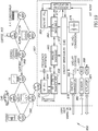
- FIG. 19 A block diagram illustrating an example IoT node incorporating the oscillator/frequency generator is shown in Figure 19 .
- the example IoT generally referenced 950, comprises a plurality of nodes 990.
- the architecture of an example IoT node 952 shown can be fully integrated as a System on Chip (SoC) on a single IC chip in nanoscale CMOS. It contains the radio subsystem to wirelessly communicate with other nodes and gateways 992, application processor to impart a certain amount of local "intelligence", sensor and an optional actuator to interface with the environment and energy management to harvest energy (light, heat, vibration or RF power) from the environment and/or convert the voltage levels to those required by the functional circuitry.
- SoC System on Chip
- the RF and non-RF frequency synthesizers provide local oscillator and processor clocks, respectively.
- a frequency reference 994 provides a fixed clock with excellent long term stability to the frequency synthesizers.
- the power amplifier described supra is incorporated in the RF transceiver 958 as circuit block 970.
- the RF transceiver 958 interfaces with an antenna 956.
- the RF signals are upconverted and downconverted there to the lower (i.e. baseband) frequencies, which are then processed in the analog baseband circuitry.
- the digital baseband completes the physical layer of a chosen communication standard.
- the application processor performs various control and signal processing functions and is responsible for giving a level of "intelligence" to the IoT node.
- the RF frequency synthesizer 954 is realized as an all-digital PLL (ADPLL) and provides a local oscillator signal to the RF transceiver 958.
- the non-RF frequency synthesizer 964 provides clocks to the digital baseband 962 and application processors 974.
- the clock frequency has to be dynamically switchable in response to the changing computational load conditions.
- the energy management (EM) circuitry 972 provides energy conversion between the energy harvester 978 and/or low-capacity storage battery 980 and all the IoT functional circuits. The EM circuit carries out several functions.
- boosts the voltage from the energy harvester e.g., light, heat, vibration, RF electromagnetic, etc.
- the energy harvester e.g., light, heat, vibration, RF electromagnetic, etc.
- boost converter 976 boosts the voltage from the energy harvester (e.g., light, heat, vibration, RF electromagnetic, etc.) to that required by the nanoscale CMOS circuits, which is in the range of 0.7 to 1.0 V assuming 40 nm CMOS technology.
- boost converter 976 boost converter 976.
- boost and buck converters use energy storage passive devices, i.e. capacitor or inductor for storing electrical and magnetic energy, respectively, in order to change the voltage level with high efficiency.
- the EM needs to provide many power supply domains. This is dictated by the different voltage level requirements during voltage scaling.
- the EM supply domains preferably provide individually adjustable voltage levels.
- the supply voltage level of digital logic circuits widely vary depending on the fast changing real time computational load conditions, while the voltage level of digital RF and analog circuits experience less of such variance, and mainly due to temperature and operating frequency, as well as communication channel conditions.
- the analog circuits have to be properly biased, which normally prevents them from operating at near-threshold conditions.
Landscapes
- Engineering & Computer Science (AREA)
- Power Engineering (AREA)
- Amplifiers (AREA)
- Transmitters (AREA)
Claims (10)
- Diviseur de signal radiofréquence, RF, (38, 180, 260), comprenant :un transformateur ayant :un enroulement primaire (262) pour recevoir un signal d'entrée différentiel ;un premier enroulement secondaire (266, 184) ayant un premier port et un deuxième port et configuré pour générer un premier signal de sortie différentiel ;un deuxième enroulement secondaire (264, 186) ayant un troisième port et un quatrième port et configuré pour générer un deuxième signal de sortie différentiel ; etune connexion transversale (188, 268, 270) connectant électriquement ledit premier port dudit premier enroulement secondaire audit quatrième port dudit deuxième enroulement secondaire ainsi que connectant électriquement ledit deuxième port dudit premier enroulement secondaire audit troisième port dudit deuxième enroulement secondaire.
- Diviseur de signal selon la revendication 1, dans lequel ladite connexion transversale (188, 268, 270) connecte électriquement des ports en phase desdits premier (266, 184) et deuxième (264, 186) enroulements secondaires l'un à l'autre.
- Diviseur de signal selon la revendication 1, dans lequel ladite connexion transversale (188, 268, 270) fonctionne pour réduire le gain de boucle d'une combinaison d'oscillations de mode différentiel et de mode commun.
- Diviseur de signal selon la revendication 1, dans lequel ladite connexion transversale (188, 268, 270) n'affecte pas le fonctionnement normal dudit diviseur.
- Diviseur de signal selon la revendication 1, dans lequel ladite connexion transversale (188, 268, 270) fonctionne pour introduire une perte de signal dans un retour desdits premier et deuxième signaux de sortie différentiels.
- Diviseur de signal radiofréquence, RF, de l'une des revendications précédentes, dans lequel :le premier enroulement secondaire (266, 184) a un port de première polarité et un port de deuxième polarité opposée ;le deuxième enroulement secondaire (264, 186) a un port de première polarité et un port de deuxième polarité opposée ;la connexion transversale (188, 268, 270) est configurée pour connecter électriquement le port de première polarité dudit premier enroulement secondaire au port de première polarité dudit deuxième enroulement secondaire, et pour connecter électriquement le port de deuxième polarité dudit premier enroulement secondaire au port de deuxième polarité dudit deuxième enroulement secondaire ; etladite connexion transversale (188, 268, 270) ayant une largeur au moins quatre fois plus étroite que ledit premier enroulement secondaire et ledit deuxième enroulement secondaire, ladite connexion transversale fonctionnant ainsi pour amortir des oscillations combinées de mode commun et de mode différentiel présentes sur lesdits premier et deuxième enroulements secondaires.
- Procédé pour fournir un diviseur de signal RF, comprenant les étapes consistant à :fournir un enroulement primaire (262) pour recevoir un signal d'entrée différentiel ;fournir un premier enroulement secondaire (266) ayant un premier port et un deuxième port, et configuré pour générer un premier signal de sortie différentiel ;fournir un deuxième enroulement secondaire (264) ayant un troisième port et un quatrième port, et configuré pour générer un deuxième signal de sortie différentiel ;connecter électriquement ledit premier port dudit premier enroulement secondaire audit quatrième port dudit deuxième enroulement secondaire via une première connexion électrique (188, 268, 270) ;connecter électriquement ledit deuxième port dudit premier enroulement secondaire audit troisième port dudit deuxième enroulement secondaire via une deuxième connexion électrique (188, 268, 270) ; etdans lequel une section transversale de ladite première connexion électrique et de ladite deuxième connexion électrique est suffisamment inférieure à celle dudit premier enroulement secondaire et dudit deuxième enroulement secondaire pour réduire efficacement un gain de boucle d'une combinaison d'oscillations de mode différentiel et de mode commun.
- Procédé selon la revendication 7, comprenant en outre le placement de ladite première connexion électrique et de ladite deuxième connexion électrique (268, 270) entre des ports en phase desdits premier enroulement secondaire et deuxième enroulement secondaire.
- Procédé selon la revendication 7, dans lequel ladite première connexion électrique et ladite deuxième connexion électrique (268, 270) fonctionnent pour introduire une perte de signal dans un retour du premier signal de sortie différentiel et dudit deuxième signal de sortie différentiel.
- Procédé selon la revendication 7, dans lequel ladite première connexion électrique et ladite deuxième connexion électrique (268, 270) n'affectent pas le fonctionnement normal dudit diviseur de signal RF.
Applications Claiming Priority (2)
| Application Number | Priority Date | Filing Date | Title |
|---|---|---|---|
| US201462059448P | 2014-10-03 | 2014-10-03 | |
| PCT/US2015/053900 WO2016054619A1 (fr) | 2014-10-03 | 2015-10-03 | Amplificateur de puissance e/f2 de classe à large bande 60 ghz |
Publications (3)
| Publication Number | Publication Date |
|---|---|
| EP3202032A1 EP3202032A1 (fr) | 2017-08-09 |
| EP3202032A4 EP3202032A4 (fr) | 2018-09-05 |
| EP3202032B1 true EP3202032B1 (fr) | 2021-09-22 |
Family
ID=55631677
Family Applications (2)
| Application Number | Title | Priority Date | Filing Date |
|---|---|---|---|
| EP15847423.9A Active EP3202032B1 (fr) | 2014-10-03 | 2015-10-03 | Separateur de frequence pour signaux rf pour un amplificateur de puissance e/f2 de classe à large bande 60 ghz |
| EP15847809.9A Active EP3219017B1 (fr) | 2014-10-03 | 2015-10-03 | Réseau d'adaptation d'impédance basé sur un transformateur |
Family Applications After (1)
| Application Number | Title | Priority Date | Filing Date |
|---|---|---|---|
| EP15847809.9A Active EP3219017B1 (fr) | 2014-10-03 | 2015-10-03 | Réseau d'adaptation d'impédance basé sur un transformateur |
Country Status (3)
| Country | Link |
|---|---|
| US (4) | US9634610B2 (fr) |
| EP (2) | EP3202032B1 (fr) |
| WO (2) | WO2016054617A2 (fr) |
Families Citing this family (52)
| Publication number | Priority date | Publication date | Assignee | Title |
|---|---|---|---|---|
| WO2016054617A2 (fr) * | 2014-10-03 | 2016-04-07 | Zaretsky, Howard | Réseau d'adaptation d'impédance basé sur un transformateur et amplificateur de puissance associé, adpll et émetteur basé sur cette adpll |
| US10654365B2 (en) * | 2015-04-29 | 2020-05-19 | Aptiv Technologies Limited | Bifurcated balanced electromagnetic resonator |
| CN105897194B (zh) * | 2016-05-11 | 2019-03-05 | 杭州电子科技大学 | 一种连续ef类高效率宽带功率放大器及其实现方法 |
| DE102016111887B4 (de) * | 2016-06-29 | 2026-04-30 | Infineon Technologies Ag | Differentieller Richtkoppler, Signalumwandlungssystem und Verfahren zur Umwandlung eines differentiellen Eingangssignals |
| US11686805B1 (en) | 2016-07-10 | 2023-06-27 | ZaiNar, Inc. | Method and system for radiofrequency localization of transmitting devices via a mesh network |
| WO2018010180A1 (fr) * | 2016-07-15 | 2018-01-18 | 华为技术有限公司 | Oscillateur |
| TWM535833U (zh) * | 2016-08-25 | 2017-01-21 | Ma Frank Tsu-Yuan | 應用藍牙技術之短距媒合模組 |
| US10235614B1 (en) * | 2016-11-01 | 2019-03-19 | National Technology & Engineering Solutions Of Sandia, Llc | Communication device and method of making the same |
| US10250076B2 (en) | 2017-03-15 | 2019-04-02 | Hong Kong Applied Science And Technology Research Institute Co., Ltd. | Wireless power transmitter |
| KR102387572B1 (ko) | 2017-04-20 | 2022-04-18 | 삼성전자주식회사 | 무선 통신 장치 및 방법 |
| EP3404832B1 (fr) * | 2017-05-18 | 2020-02-12 | IMEC vzw | Dispositif de changement de phase rf |
| US20190189342A1 (en) * | 2017-12-20 | 2019-06-20 | National Chung Shan Institute Of Science And Technology | Variable inductor and integrated circuit using the variable inductor |
| US10985709B2 (en) * | 2018-03-15 | 2021-04-20 | Taiwan Semiconductor Manufacturing Co., Ltd. | Systems and methods for suppressing and mitigating harmonic distortion in a circuit |
| US11018628B2 (en) * | 2018-03-31 | 2021-05-25 | Skyworks Solutions, Inc. | Antenna impedance prediction via power amplifier parameter |
| US10911211B1 (en) | 2018-09-28 | 2021-02-02 | ZaiNar, Inc. | Frequency and gain calibration for time synchronization in a network |
| US11658798B1 (en) | 2018-05-07 | 2023-05-23 | ZaiNar, Inc. | Methods for time synchronization and localization in a mesh network |
| US10833840B2 (en) | 2018-05-07 | 2020-11-10 | ZaiNar, Inc. | Methods for nanosecond-scale time synchronization over a network |
| US11722979B2 (en) | 2019-04-10 | 2023-08-08 | ZaiNar, Inc. | Method for precise timestamping of narrowband signals in the presence of multipath |
| DE102018215763A1 (de) * | 2018-09-17 | 2020-03-19 | Bayerische Motoren Werke Aktiengesellschaft | Rundfunk-Empfangseinrichtung eines Kraftfahrzeugs |
| CN109245735B (zh) * | 2018-10-18 | 2023-10-27 | 成都嘉纳海威科技有限责任公司 | 一种基于二次谐波注入技术的高效率j类堆叠功率放大器 |
| CN109406854B (zh) * | 2018-10-24 | 2021-07-06 | 广东工业大学 | 单相有源滤波器的谐波指令电流获取方法、装置及设备 |
| US10938358B2 (en) | 2018-10-31 | 2021-03-02 | Kabushiki Kaisha Toshiba | Digital power amplifier |
| US12121318B2 (en) * | 2019-02-15 | 2024-10-22 | The Regents Of The University Of California | Low power magnetic field body area network with quenching and quick start |
| US11615279B1 (en) * | 2019-04-29 | 2023-03-28 | ZaiNar, Inc. | Radio-frequency system characterized by flat group delay for radio-frequency time synchronization and ranging |
| CN110535447A (zh) * | 2019-06-23 | 2019-12-03 | 复旦大学 | 适用于射频功放的八路功率合成谐波控制功率放大电路 |
| TWI730372B (zh) * | 2019-08-07 | 2021-06-11 | 瑞昱半導體股份有限公司 | 無線傳輸電路與控制方法 |
| CN112398501B (zh) * | 2019-08-15 | 2022-04-26 | 瑞昱半导体股份有限公司 | 无线传输电路与控制方法 |
| US11356069B2 (en) | 2019-10-21 | 2022-06-07 | Kabushiki Kaisha Toshiba | Digital power amplifier |
| US11206000B1 (en) * | 2019-11-26 | 2021-12-21 | Rockwell Collins, Inc. | Filterless high efficiency class D power amplifier |
| US11785482B1 (en) | 2019-11-26 | 2023-10-10 | ZaiNar, Inc. | Method for identifying and diagnosing failures in pairwise time synchronization and frequency calibration in a mesh network |
| US11863298B1 (en) | 2019-11-26 | 2024-01-02 | ZaiNar, Inc. | Method for identifying and diagnosing failures in pairwise time synchronization and frequency calibration in a mesh network |
| EP3829068B1 (fr) * | 2019-11-29 | 2025-10-15 | Socionext Inc. | Circuit de transformateur |
| US10911078B1 (en) | 2020-02-14 | 2021-02-02 | The Regents Of The University Of Michigan | Millimeter-scale bluetooth low energy transmitter with dual purpose loop antenna |
| CN111259598B (zh) * | 2020-03-30 | 2022-05-20 | 西安交通大学 | 一种陶瓷绝缘干式变压器散热结构优化设计方法 |
| CN111884606A (zh) * | 2020-06-22 | 2020-11-03 | 南京迈矽科微电子科技有限公司 | 基于毫米波变压器的宽带匹配电路及毫米波功率放大电路 |
| US11394354B2 (en) | 2020-06-29 | 2022-07-19 | Kabushiki Kaisha Toshiba | Digital power amplifier and method of optimising a digital power amplifier |
| US11437699B2 (en) * | 2020-07-22 | 2022-09-06 | Bae Systems Information And Electronic Systems Integration Inc. | Multiport matched RF power splitter |
| WO2022028695A1 (fr) * | 2020-08-05 | 2022-02-10 | Telefonaktiebolaget Lm Ericsson (Publ) | Déphaseur rf |
| US11689162B2 (en) | 2020-08-21 | 2023-06-27 | Samsung Electronics Co., Ltd. | 24 to 30GHz wide band CMOS power amplifier with turn-off mode high impedance |
| EP4232839A4 (fr) | 2020-10-26 | 2024-06-26 | Zainar, Inc. | Procédé hybride de télémétrie basée sur le temps d'arrivée |
| CN112332806B (zh) * | 2020-11-19 | 2024-02-02 | 南京汇君半导体科技有限公司 | 一种高增益低噪声射频移相器 |
| CN114597631B (zh) * | 2020-12-07 | 2025-05-13 | Oppo广东移动通信有限公司 | 电子设备 |
| WO2022122115A1 (fr) * | 2020-12-07 | 2022-06-16 | Telefonaktiebolaget Lm Ericsson (Publ) | Agencement d'amplificateur à rejet d'harmoniques amélioré |
| CN113206644B (zh) * | 2021-03-24 | 2022-05-27 | 电子科技大学 | 一种带宽可重构的高效率分布式功率放大器 |
| WO2022265728A2 (fr) * | 2021-04-25 | 2022-12-22 | University Of Southern California | Amplificateur de puissance de classe ef à ondes millimétriques avec réglage simultané des harmoniques et des sous-harmoniques |
| CN118339766A (zh) * | 2021-12-08 | 2024-07-12 | 株式会社村田制作所 | 放大装置 |
| CN116846351B (zh) * | 2022-03-23 | 2025-04-22 | 锐石创芯(深圳)科技股份有限公司 | 推挽功率放大电路 |
| US12513491B2 (en) | 2022-04-20 | 2025-12-30 | ZaiNar, Inc. | Methods for asset tag grouping and recovery |
| CN118740073A (zh) * | 2023-03-31 | 2024-10-01 | 锐石创芯(深圳)科技股份有限公司 | 推挽功率放大电路、推挽功率放大器和射频前端模组 |
| US20250279564A1 (en) * | 2024-03-01 | 2025-09-04 | Apple Inc. | Compact phase shifter layout |
| US12549132B2 (en) | 2024-05-02 | 2026-02-10 | Apple Inc. | Transformer based filter for complementary oscillator circuitry |
| US12537480B2 (en) | 2024-05-08 | 2026-01-27 | Apple Inc. | Phase noise filter for oscillator circuitry |
Family Cites Families (28)
| Publication number | Priority date | Publication date | Assignee | Title |
|---|---|---|---|---|
| US3319149A (en) | 1963-08-08 | 1967-05-09 | Cole E K Ltd | Protective circuit arrangement for semiconductor switches in static inverters |
| US3801871A (en) * | 1973-04-23 | 1974-04-02 | Amf Inc | Gfi circuit having tuned circuit fault detector |
| US4346341A (en) * | 1981-03-02 | 1982-08-24 | General Electric Company | Method and apparatus for automatic voltage reduction control |
| GB9217679D0 (en) * | 1992-08-20 | 1992-09-30 | Marconi Gec Ltd | Combiners for r.f.power amplifiers |
| US5247264A (en) | 1992-09-04 | 1993-09-21 | Broadcast Electronics, Inc. | Combining circuit for Class-E RF power amplifiers |
| US5467013A (en) * | 1993-12-07 | 1995-11-14 | Sematech, Inc. | Radio frequency monitor for semiconductor process control |
| US6026286A (en) * | 1995-08-24 | 2000-02-15 | Nortel Networks Corporation | RF amplifier, RF mixer and RF receiver |
| US6549071B1 (en) | 2000-09-12 | 2003-04-15 | Silicon Laboratories, Inc. | Power amplifier circuitry and method using an inductance coupled to power amplifier switching devices |
| CN1295865C (zh) * | 2000-10-10 | 2007-01-17 | 加利福尼亚技术协会 | E/f类开关功率放大器 |
| FI116108B (fi) | 2003-06-24 | 2005-09-15 | Esju Oy | Amplitudisäädin |
| US7292126B2 (en) | 2004-04-30 | 2007-11-06 | Astec International Limited | Low noise planar transformer |
| US7372336B2 (en) | 2004-12-31 | 2008-05-13 | Samsung Electronics Co., Ltd. | Small-sized on-chip CMOS power amplifier having improved efficiency |
| US7288991B2 (en) * | 2005-02-17 | 2007-10-30 | Skyworks Solutions, Inc. | Power control circuit for accurate control of power amplifier output power |
| US7872881B2 (en) * | 2005-08-17 | 2011-01-18 | Adc Dsl Systems, Inc. | Secondary regulation in a multiple output flyback topology |
| US7576607B2 (en) * | 2008-01-03 | 2009-08-18 | Samsung Electro-Mechanics | Multi-segment primary and multi-turn secondary transformer for power amplifier systems |
| US7683733B2 (en) * | 2008-02-04 | 2010-03-23 | Freescale Semiconductor, Inc. | Balun transformer with improved harmonic suppression |
| US7777570B2 (en) | 2008-03-12 | 2010-08-17 | Mediatek Inc. | Transformer power combiner having secondary winding conductors magnetically coupled to primary winding conductors and configured in topology including series connection and parallel connection |
| JP5218112B2 (ja) | 2009-02-03 | 2013-06-26 | 富士通株式会社 | 電力分配回路 |
| JP5075958B2 (ja) * | 2010-09-09 | 2012-11-21 | 株式会社東芝 | 高周波スイッチ回路および無線通信装置 |
| EP2549645A1 (fr) * | 2011-07-21 | 2013-01-23 | Telefonaktiebolaget LM Ericsson (publ) | Agencement de filtre de transformateur |
| JP5828069B2 (ja) | 2011-07-27 | 2015-12-02 | パナソニックIpマネジメント株式会社 | 電力分配回路 |
| US9294067B2 (en) * | 2011-11-03 | 2016-03-22 | Rf Micro Devices, Inc. | Combined balun transformer and harmonic filter |
| US8576013B2 (en) * | 2011-12-29 | 2013-11-05 | Mks Instruments, Inc. | Power distortion-based servo control systems for frequency tuning RF power sources |
| TW201342402A (zh) * | 2012-04-06 | 2013-10-16 | Realtek Semiconductor Corp | 晶載式多繞組變壓器 |
| EP2669906B1 (fr) * | 2012-06-01 | 2018-08-29 | Nxp B.V. | Transformateur à base de circuit intégré |
| US9197221B2 (en) | 2012-09-16 | 2015-11-24 | Technische Universiteit Delft | Class-F CMOS oscillator incorporating differential passive network |
| US8781415B1 (en) * | 2013-02-07 | 2014-07-15 | Mks Instruments, Inc. | Distortion correction based feedforward control systems and methods for radio frequency power sources |
| WO2016054617A2 (fr) * | 2014-10-03 | 2016-04-07 | Zaretsky, Howard | Réseau d'adaptation d'impédance basé sur un transformateur et amplificateur de puissance associé, adpll et émetteur basé sur cette adpll |
-
2015
- 2015-10-03 WO PCT/US2015/053898 patent/WO2016054617A2/fr not_active Ceased
- 2015-10-03 EP EP15847423.9A patent/EP3202032B1/fr active Active
- 2015-10-03 EP EP15847809.9A patent/EP3219017B1/fr active Active
- 2015-10-03 US US14/874,427 patent/US9634610B2/en active Active
- 2015-10-03 US US14/874,422 patent/US10110195B2/en active Active
- 2015-10-03 WO PCT/US2015/053900 patent/WO2016054619A1/fr not_active Ceased
- 2015-10-03 US US14/874,421 patent/US9685910B2/en not_active Expired - Fee Related
-
2017
- 2017-05-02 US US15/584,257 patent/US9831847B2/en active Active
Also Published As
| Publication number | Publication date |
|---|---|
| WO2016054617A2 (fr) | 2016-04-07 |
| US9831847B2 (en) | 2017-11-28 |
| US10110195B2 (en) | 2018-10-23 |
| EP3202032A4 (fr) | 2018-09-05 |
| WO2016054617A3 (fr) | 2016-05-26 |
| US20160099685A1 (en) | 2016-04-07 |
| EP3219017B1 (fr) | 2021-11-10 |
| EP3202032A1 (fr) | 2017-08-09 |
| US20160099691A1 (en) | 2016-04-07 |
| EP3219017A4 (fr) | 2018-06-13 |
| US9685910B2 (en) | 2017-06-20 |
| EP3219017A2 (fr) | 2017-09-20 |
| US20160099700A1 (en) | 2016-04-07 |
| US9634610B2 (en) | 2017-04-25 |
| WO2016054619A1 (fr) | 2016-04-07 |
| US20170237407A1 (en) | 2017-08-17 |
Similar Documents
| Publication | Publication Date | Title |
|---|---|---|
| EP3202032B1 (fr) | Separateur de frequence pour signaux rf pour un amplificateur de puissance e/f2 de classe à large bande 60 ghz | |
| US9866178B2 (en) | Radio frequency circuitr having an integrated harmonic filter and a radio frequency circuit having transistors of different threshold voltages | |
| US10903806B2 (en) | Radio frequency circuitr having an integrated harmonic filter and a radio frequency circuit having transistors of different threshold voltages | |
| TWI514753B (zh) | 功率放大器 | |
| CN105409116B (zh) | 具有可配置的相互耦合的源极退化电感器的放大器 | |
| US7768350B2 (en) | Output gain stage for a power amplifier | |
| Chowdhury et al. | A fully integrated dual-mode highly linear 2.4 GHz CMOS power amplifier for 4G WiMax applications | |
| US9484977B2 (en) | RF transformer based TX/RX integrated RF switch | |
| CN104682884B (zh) | 用于功率放大器中的相位补偿的装置和方法 | |
| CN104467745B (zh) | 动态误差向量幅度占空比校正 | |
| CN104067513B (zh) | 具有可调谐负载匹配的多模旁路激励放大器 | |
| US9667206B2 (en) | Linear row array integrated power combiner for RF power amplifiers | |
| CN105103442A (zh) | 具有经助推或经制推的源极退化电感的放大器 | |
| Sessou et al. | An Integrated 700–1200-MHz Class-F PA With Tunable Harmonic Terminations in 0.13-$\mu $ m CMOS | |
| CN104160553A (zh) | 基于cmos的rf天线开关 | |
| US20170187338A1 (en) | Amplifier with coupled inductors |
Legal Events
| Date | Code | Title | Description |
|---|---|---|---|
| STAA | Information on the status of an ep patent application or granted ep patent |
Free format text: STATUS: THE INTERNATIONAL PUBLICATION HAS BEEN MADE |
|
| PUAI | Public reference made under article 153(3) epc to a published international application that has entered the european phase |
Free format text: ORIGINAL CODE: 0009012 |
|
| STAA | Information on the status of an ep patent application or granted ep patent |
Free format text: STATUS: REQUEST FOR EXAMINATION WAS MADE |
|
| 17P | Request for examination filed |
Effective date: 20170503 |
|
| AK | Designated contracting states |
Kind code of ref document: A1 Designated state(s): AL AT BE BG CH CY CZ DE DK EE ES FI FR GB GR HR HU IE IS IT LI LT LU LV MC MK MT NL NO PL PT RO RS SE SI SK SM TR |
|
| AX | Request for extension of the european patent |
Extension state: BA ME |
|
| DAV | Request for validation of the european patent (deleted) | ||
| DAX | Request for extension of the european patent (deleted) | ||
| A4 | Supplementary search report drawn up and despatched |
Effective date: 20180806 |
|
| RIC1 | Information provided on ipc code assigned before grant |
Ipc: H03H 7/42 20060101ALI20180731BHEP Ipc: H03H 7/48 20060101ALI20180731BHEP Ipc: H03F 3/217 20060101ALN20180731BHEP Ipc: H03F 3/193 20060101ALN20180731BHEP Ipc: H03F 1/56 20060101ALN20180731BHEP Ipc: H03H 7/38 20060101ALN20180731BHEP Ipc: H03H 7/09 20060101ALI20180731BHEP Ipc: H03F 3/189 20060101AFI20180731BHEP Ipc: H01F 27/34 20060101ALN20180731BHEP Ipc: H03F 1/02 20060101ALN20180731BHEP Ipc: H03F 3/24 20060101ALN20180731BHEP |
|
| STAA | Information on the status of an ep patent application or granted ep patent |
Free format text: STATUS: EXAMINATION IS IN PROGRESS |
|
| 17Q | First examination report despatched |
Effective date: 20200504 |
|
| RIC1 | Information provided on ipc code assigned before grant |
Ipc: H03H 7/48 20060101ALI20210212BHEP Ipc: H03F 3/217 20060101ALN20210212BHEP Ipc: H03F 3/189 20060101AFI20210212BHEP Ipc: H03H 7/42 20060101ALI20210212BHEP Ipc: H03H 7/09 20060101ALI20210212BHEP Ipc: H03F 3/193 20060101ALN20210212BHEP Ipc: H03F 1/56 20060101ALN20210212BHEP Ipc: H01F 27/34 20060101ALN20210212BHEP Ipc: H03F 1/02 20060101ALN20210212BHEP Ipc: H03H 7/38 20060101ALN20210212BHEP Ipc: H03F 3/24 20060101ALN20210212BHEP |
|
| RIC1 | Information provided on ipc code assigned before grant |
Ipc: H03H 7/38 20060101ALN20210304BHEP Ipc: H03H 7/09 20060101ALI20210304BHEP Ipc: H03F 1/02 20060101ALN20210304BHEP Ipc: H03F 3/189 20060101AFI20210304BHEP Ipc: H03F 3/217 20060101ALN20210304BHEP Ipc: H03F 1/56 20060101ALN20210304BHEP Ipc: H03F 3/24 20060101ALN20210304BHEP Ipc: H03H 7/48 20060101ALI20210304BHEP Ipc: H01F 27/34 20060101ALN20210304BHEP Ipc: H03H 7/42 20060101ALI20210304BHEP Ipc: H03F 3/193 20060101ALN20210304BHEP |
|
| GRAP | Despatch of communication of intention to grant a patent |
Free format text: ORIGINAL CODE: EPIDOSNIGR1 |
|
| STAA | Information on the status of an ep patent application or granted ep patent |
Free format text: STATUS: GRANT OF PATENT IS INTENDED |
|
| RIC1 | Information provided on ipc code assigned before grant |
Ipc: H01F 27/34 20060101ALN20210318BHEP Ipc: H03H 7/38 20060101ALN20210318BHEP Ipc: H03F 3/24 20060101ALN20210318BHEP Ipc: H03F 3/217 20060101ALN20210318BHEP Ipc: H03F 3/193 20060101ALN20210318BHEP Ipc: H03F 1/56 20060101ALN20210318BHEP Ipc: H03F 1/02 20060101ALN20210318BHEP Ipc: H03H 7/42 20060101ALI20210318BHEP Ipc: H03H 7/48 20060101ALI20210318BHEP Ipc: H03H 7/09 20060101ALI20210318BHEP Ipc: H03F 3/189 20060101AFI20210318BHEP |
|
| INTG | Intention to grant announced |
Effective date: 20210412 |
|
| RIN1 | Information on inventor provided before grant (corrected) |
Inventor name: STASZEWSKI, ROBERT BOGDAN Inventor name: BABAIE, MASOUD |
|
| GRAS | Grant fee paid |
Free format text: ORIGINAL CODE: EPIDOSNIGR3 |
|
| GRAA | (expected) grant |
Free format text: ORIGINAL CODE: 0009210 |
|
| STAA | Information on the status of an ep patent application or granted ep patent |
Free format text: STATUS: THE PATENT HAS BEEN GRANTED |
|
| RAP1 | Party data changed (applicant data changed or rights of an application transferred) |
Owner name: SHORT CIRCUIT TECHNOLOGIES LLC |
|
| AK | Designated contracting states |
Kind code of ref document: B1 Designated state(s): AL AT BE BG CH CY CZ DE DK EE ES FI FR GB GR HR HU IE IS IT LI LT LU LV MC MK MT NL NO PL PT RO RS SE SI SK SM TR |
|
| REG | Reference to a national code |
Ref country code: GB Ref legal event code: FG4D |
|
| REG | Reference to a national code |
Ref country code: DE Ref legal event code: R096 Ref document number: 602015073580 Country of ref document: DE |
|
| REG | Reference to a national code |
Ref country code: IE Ref legal event code: FG4D |
|
| REG | Reference to a national code |
Ref country code: CH Ref legal event code: EP Ref country code: AT Ref legal event code: REF Ref document number: 1433106 Country of ref document: AT Kind code of ref document: T Effective date: 20211015 |
|
| REG | Reference to a national code |
Ref country code: LT Ref legal event code: MG9D |
|
| REG | Reference to a national code |
Ref country code: NL Ref legal event code: MP Effective date: 20210922 |
|
| PG25 | Lapsed in a contracting state [announced via postgrant information from national office to epo] |
Ref country code: HR Free format text: LAPSE BECAUSE OF FAILURE TO SUBMIT A TRANSLATION OF THE DESCRIPTION OR TO PAY THE FEE WITHIN THE PRESCRIBED TIME-LIMIT Effective date: 20210922 Ref country code: RS Free format text: LAPSE BECAUSE OF FAILURE TO SUBMIT A TRANSLATION OF THE DESCRIPTION OR TO PAY THE FEE WITHIN THE PRESCRIBED TIME-LIMIT Effective date: 20210922 Ref country code: SE Free format text: LAPSE BECAUSE OF FAILURE TO SUBMIT A TRANSLATION OF THE DESCRIPTION OR TO PAY THE FEE WITHIN THE PRESCRIBED TIME-LIMIT Effective date: 20210922 Ref country code: NO Free format text: LAPSE BECAUSE OF FAILURE TO SUBMIT A TRANSLATION OF THE DESCRIPTION OR TO PAY THE FEE WITHIN THE PRESCRIBED TIME-LIMIT Effective date: 20211222 Ref country code: FI Free format text: LAPSE BECAUSE OF FAILURE TO SUBMIT A TRANSLATION OF THE DESCRIPTION OR TO PAY THE FEE WITHIN THE PRESCRIBED TIME-LIMIT Effective date: 20210922 Ref country code: LT Free format text: LAPSE BECAUSE OF FAILURE TO SUBMIT A TRANSLATION OF THE DESCRIPTION OR TO PAY THE FEE WITHIN THE PRESCRIBED TIME-LIMIT Effective date: 20210922 Ref country code: BG Free format text: LAPSE BECAUSE OF FAILURE TO SUBMIT A TRANSLATION OF THE DESCRIPTION OR TO PAY THE FEE WITHIN THE PRESCRIBED TIME-LIMIT Effective date: 20211222 |
|
| REG | Reference to a national code |
Ref country code: AT Ref legal event code: MK05 Ref document number: 1433106 Country of ref document: AT Kind code of ref document: T Effective date: 20210922 |
|
| PG25 | Lapsed in a contracting state [announced via postgrant information from national office to epo] |
Ref country code: LV Free format text: LAPSE BECAUSE OF FAILURE TO SUBMIT A TRANSLATION OF THE DESCRIPTION OR TO PAY THE FEE WITHIN THE PRESCRIBED TIME-LIMIT Effective date: 20210922 Ref country code: GR Free format text: LAPSE BECAUSE OF FAILURE TO SUBMIT A TRANSLATION OF THE DESCRIPTION OR TO PAY THE FEE WITHIN THE PRESCRIBED TIME-LIMIT Effective date: 20211223 |
|
| PG25 | Lapsed in a contracting state [announced via postgrant information from national office to epo] |
Ref country code: AT Free format text: LAPSE BECAUSE OF FAILURE TO SUBMIT A TRANSLATION OF THE DESCRIPTION OR TO PAY THE FEE WITHIN THE PRESCRIBED TIME-LIMIT Effective date: 20210922 |
|
| REG | Reference to a national code |
Ref country code: CH Ref legal event code: PL |
|
| PG25 | Lapsed in a contracting state [announced via postgrant information from national office to epo] |
Ref country code: IS Free format text: LAPSE BECAUSE OF FAILURE TO SUBMIT A TRANSLATION OF THE DESCRIPTION OR TO PAY THE FEE WITHIN THE PRESCRIBED TIME-LIMIT Effective date: 20220122 Ref country code: SK Free format text: LAPSE BECAUSE OF FAILURE TO SUBMIT A TRANSLATION OF THE DESCRIPTION OR TO PAY THE FEE WITHIN THE PRESCRIBED TIME-LIMIT Effective date: 20210922 Ref country code: RO Free format text: LAPSE BECAUSE OF FAILURE TO SUBMIT A TRANSLATION OF THE DESCRIPTION OR TO PAY THE FEE WITHIN THE PRESCRIBED TIME-LIMIT Effective date: 20210922 Ref country code: PT Free format text: LAPSE BECAUSE OF FAILURE TO SUBMIT A TRANSLATION OF THE DESCRIPTION OR TO PAY THE FEE WITHIN THE PRESCRIBED TIME-LIMIT Effective date: 20220124 Ref country code: PL Free format text: LAPSE BECAUSE OF FAILURE TO SUBMIT A TRANSLATION OF THE DESCRIPTION OR TO PAY THE FEE WITHIN THE PRESCRIBED TIME-LIMIT Effective date: 20210922 Ref country code: NL Free format text: LAPSE BECAUSE OF FAILURE TO SUBMIT A TRANSLATION OF THE DESCRIPTION OR TO PAY THE FEE WITHIN THE PRESCRIBED TIME-LIMIT Effective date: 20210922 Ref country code: ES Free format text: LAPSE BECAUSE OF FAILURE TO SUBMIT A TRANSLATION OF THE DESCRIPTION OR TO PAY THE FEE WITHIN THE PRESCRIBED TIME-LIMIT Effective date: 20210922 Ref country code: EE Free format text: LAPSE BECAUSE OF FAILURE TO SUBMIT A TRANSLATION OF THE DESCRIPTION OR TO PAY THE FEE WITHIN THE PRESCRIBED TIME-LIMIT Effective date: 20210922 Ref country code: CZ Free format text: LAPSE BECAUSE OF FAILURE TO SUBMIT A TRANSLATION OF THE DESCRIPTION OR TO PAY THE FEE WITHIN THE PRESCRIBED TIME-LIMIT Effective date: 20210922 Ref country code: AL Free format text: LAPSE BECAUSE OF FAILURE TO SUBMIT A TRANSLATION OF THE DESCRIPTION OR TO PAY THE FEE WITHIN THE PRESCRIBED TIME-LIMIT Effective date: 20210922 |
|
| REG | Reference to a national code |
Ref country code: DE Ref legal event code: R097 Ref document number: 602015073580 Country of ref document: DE Ref country code: BE Ref legal event code: MM Effective date: 20211031 |
|
| PG25 | Lapsed in a contracting state [announced via postgrant information from national office to epo] |
Ref country code: MC Free format text: LAPSE BECAUSE OF FAILURE TO SUBMIT A TRANSLATION OF THE DESCRIPTION OR TO PAY THE FEE WITHIN THE PRESCRIBED TIME-LIMIT Effective date: 20210922 |
|
| PG25 | Lapsed in a contracting state [announced via postgrant information from national office to epo] |
Ref country code: LU Free format text: LAPSE BECAUSE OF NON-PAYMENT OF DUE FEES Effective date: 20211003 Ref country code: DK Free format text: LAPSE BECAUSE OF FAILURE TO SUBMIT A TRANSLATION OF THE DESCRIPTION OR TO PAY THE FEE WITHIN THE PRESCRIBED TIME-LIMIT Effective date: 20210922 Ref country code: BE Free format text: LAPSE BECAUSE OF NON-PAYMENT OF DUE FEES Effective date: 20211031 |
|
| PLBE | No opposition filed within time limit |
Free format text: ORIGINAL CODE: 0009261 |
|
| STAA | Information on the status of an ep patent application or granted ep patent |
Free format text: STATUS: NO OPPOSITION FILED WITHIN TIME LIMIT |
|
| 26N | No opposition filed |
Effective date: 20220623 |
|
| PG25 | Lapsed in a contracting state [announced via postgrant information from national office to epo] |
Ref country code: LI Free format text: LAPSE BECAUSE OF NON-PAYMENT OF DUE FEES Effective date: 20211031 Ref country code: CH Free format text: LAPSE BECAUSE OF NON-PAYMENT OF DUE FEES Effective date: 20211031 |
|
| PG25 | Lapsed in a contracting state [announced via postgrant information from national office to epo] |
Ref country code: IE Free format text: LAPSE BECAUSE OF NON-PAYMENT OF DUE FEES Effective date: 20211003 |
|
| PG25 | Lapsed in a contracting state [announced via postgrant information from national office to epo] |
Ref country code: SI Free format text: LAPSE BECAUSE OF FAILURE TO SUBMIT A TRANSLATION OF THE DESCRIPTION OR TO PAY THE FEE WITHIN THE PRESCRIBED TIME-LIMIT Effective date: 20210922 |
|
| PG25 | Lapsed in a contracting state [announced via postgrant information from national office to epo] |
Ref country code: IT Free format text: LAPSE BECAUSE OF FAILURE TO SUBMIT A TRANSLATION OF THE DESCRIPTION OR TO PAY THE FEE WITHIN THE PRESCRIBED TIME-LIMIT Effective date: 20210922 |
|
| PG25 | Lapsed in a contracting state [announced via postgrant information from national office to epo] |
Ref country code: HU Free format text: LAPSE BECAUSE OF FAILURE TO SUBMIT A TRANSLATION OF THE DESCRIPTION OR TO PAY THE FEE WITHIN THE PRESCRIBED TIME-LIMIT; INVALID AB INITIO Effective date: 20151003 |
|
| PG25 | Lapsed in a contracting state [announced via postgrant information from national office to epo] |
Ref country code: CY Free format text: LAPSE BECAUSE OF FAILURE TO SUBMIT A TRANSLATION OF THE DESCRIPTION OR TO PAY THE FEE WITHIN THE PRESCRIBED TIME-LIMIT Effective date: 20210922 |
|
| PG25 | Lapsed in a contracting state [announced via postgrant information from national office to epo] |
Ref country code: SM Free format text: LAPSE BECAUSE OF FAILURE TO SUBMIT A TRANSLATION OF THE DESCRIPTION OR TO PAY THE FEE WITHIN THE PRESCRIBED TIME-LIMIT Effective date: 20210922 |
|
| PG25 | Lapsed in a contracting state [announced via postgrant information from national office to epo] |
Ref country code: MK Free format text: LAPSE BECAUSE OF FAILURE TO SUBMIT A TRANSLATION OF THE DESCRIPTION OR TO PAY THE FEE WITHIN THE PRESCRIBED TIME-LIMIT Effective date: 20210922 |
|
| PG25 | Lapsed in a contracting state [announced via postgrant information from national office to epo] |
Ref country code: TR Free format text: LAPSE BECAUSE OF FAILURE TO SUBMIT A TRANSLATION OF THE DESCRIPTION OR TO PAY THE FEE WITHIN THE PRESCRIBED TIME-LIMIT Effective date: 20210922 |
|
| PG25 | Lapsed in a contracting state [announced via postgrant information from national office to epo] |
Ref country code: MT Free format text: LAPSE BECAUSE OF FAILURE TO SUBMIT A TRANSLATION OF THE DESCRIPTION OR TO PAY THE FEE WITHIN THE PRESCRIBED TIME-LIMIT Effective date: 20210922 |
|
| PGFP | Annual fee paid to national office [announced via postgrant information from national office to epo] |
Ref country code: DE Payment date: 20241011 Year of fee payment: 10 |
|
| PGFP | Annual fee paid to national office [announced via postgrant information from national office to epo] |
Ref country code: GB Payment date: 20241003 Year of fee payment: 10 |
|
| PGFP | Annual fee paid to national office [announced via postgrant information from national office to epo] |
Ref country code: FR Payment date: 20241022 Year of fee payment: 10 |