EP3202573A1 - Capteur optoélectronique et procédé de fabrication - Google Patents
Capteur optoélectronique et procédé de fabrication Download PDFInfo
- Publication number
- EP3202573A1 EP3202573A1 EP17151450.8A EP17151450A EP3202573A1 EP 3202573 A1 EP3202573 A1 EP 3202573A1 EP 17151450 A EP17151450 A EP 17151450A EP 3202573 A1 EP3202573 A1 EP 3202573A1
- Authority
- EP
- European Patent Office
- Prior art keywords
- optical component
- optical
- printing
- positioning device
- carrier
- Prior art date
- Legal status (The legal status is an assumption and is not a legal conclusion. Google has not performed a legal analysis and makes no representation as to the accuracy of the status listed.)
- Granted
Links
Images

Classifications
-
- G—PHYSICS
- G01—MEASURING; TESTING
- G01V—GEOPHYSICS; GRAVITATIONAL MEASUREMENTS; DETECTING MASSES OR OBJECTS; TAGS
- G01V8/00—Prospecting or detecting by optical means
- G01V8/10—Detecting, e.g. by using light barriers
-
- B—PERFORMING OPERATIONS; TRANSPORTING
- B33—ADDITIVE MANUFACTURING TECHNOLOGY
- B33Y—ADDITIVE MANUFACTURING, i.e. MANUFACTURING OF THREE-DIMENSIONAL [3D] OBJECTS BY ADDITIVE DEPOSITION, ADDITIVE AGGLOMERATION OR ADDITIVE LAYERING, e.g. BY 3D PRINTING, STEREOLITHOGRAPHY OR SELECTIVE LASER SINTERING
- B33Y80/00—Products made by additive manufacturing
Definitions
- the invention relates to a method for producing an optoelectronic sensor and to an optoelectronic sensor according to the preamble of claims 1 and 10, respectively.
- the 3D printing technology is becoming increasingly established for the flexible production of components to any specification. However, it is not yet applicable for optoelectronic sensors. It will be even longer time for the required precision for high-quality optical parts or even optics carriers with sufficiently low tolerances missing. Even that would not guarantee the above mentioned adjustment, because there must continue to be a downstream adjusted composition. With the problem of printing optical precision parts and their holders in combination with each other and with the other components of a sensor, the available 3D printing technology would be completely overburdened.
- optical components are those that contribute to the optical path of the sensor. These are usually several, but the invention is often explained for simplicity only on the basis of a single optical component, without implying any limitation, because the principle can be generalized. It is conceivable not to adjust some of the optical components, because they can do without adjustment or with a very rough adjustment. Similarly, some of the optical components may not be adjusted according to the invention but with another concept, of which some are mentioned in the introduction. In general, six degrees of freedom in position and orientation relative to the housing or relative to one or more other optical components can be considered for the adjustment, but usually only one degree of freedom for a particular optical component is relevant or several, but not all degrees of freedom are relevant.
- the invention is based on the basic idea of initially positioning the optical component freely in space with the aid of a positioning device.
- the optical component is therefore unlike the prior art just not introduced into a predetermined holder and can be adjusted without any restriction.
- an optical carrier is produced around the optical component by means of 3D printing, which fixes the optical component in the already achieved adjustment. This fixation is then permanent and remains in the sensor.
- the optical carrier and the optical component form a common component after completion of 3D printing.
- the optical carrier is printed around the optical component in the sense that both are in proper alignment with each other right after 3D printing. she For example, they are connected to each other or form a common component.
- the production of the optical carrier thus also contains the step with which the optical component is otherwise used in the optical carrier. If the 3D printing makes this possible, the optics carrier can also offer adjustment possibilities, for example several detent positions, the optical component then being in the adjusted setting after production, but this could be varied later.
- the invention has the advantage that a particularly simple and cost-effective production of optoelectronic sensors is made possible.
- Tolerances of the 3D printing play no role, because at the interface to the optical component, the fixation of the positioning ensures accurate adjustment.
- Whether the optics carrier then has a certain play of material on a side remote from the optical component is irrelevant to the function. Because of the free positioning of the optical component in the room independently of other sensor components, virtually any degree of freedom is available for an exact adjustment adapted to the task of the sensor.
- the method according to the invention allows a much faster and easier transition from development to production, and it is particularly suitable for the sample construction and small series or even individual sensors.
- the positioning device is preferably adjusted to adjust the predetermined adjustment of the optical component. In principle, it would also be conceivable to achieve the adjustment via a rigid specification of the positioning device or variations, as the optical component is held in the positioning device. It is simpler if the positioning device itself provides the required degrees of freedom for an adjustment.
- the positioning device is preferably adjusted with its own drive. It is therefore an active positioning, which does not have to be moved by hand, but which can be moved, for example, with a control unit or software to a desired location and / or rotated in a desired orientation.
- the positioning device is preferably operated by a robot or is part of a robot.
- the robot or robot arm enables an automatic process.
- the optical component is removed in an automatic sequence from a storage container and brought into the adjusted 6D position, wherein, as already mentioned above, not all degrees of freedom are generally relevant.
- a sensor function can be active, by means of which the robot tracks the optical component until the sensor function satisfies a specification.
- the positioning device is preferably removed after or during the 3D printing.
- the robot releases as soon as the 3D printing material fixes the optical component in the adjustment.
- a waiting time for curing may be required.
- a further 3D printing step is conceivable in order to complete the production of the optical carrier also over the gripping regions.
- the optical carrier is preferably produced in the 3D printing process as part of a housing or together with a housing. So it's not just an optics carrier printed, but also the case.
- further or all components of the sensor can be held by the positioning device or otherwise in the region of the 3D printing.
- the movement into the predetermined adjustment with the aid of the positioning device and the 3D printing process preferably takes place as a common production step in a production line of the sensor.
- the optical carrier is therefore not prepared in advance, but rather the responsible 3D printer is integrated into the production line, and the adjusted connection of optical carrier and optical component by 3D printing is only a partial step of the final production. This is much faster and more effective.
- the positioning device with the 3D printer is practically a universal station for a wide variety of sensors, because the optical carrier must be set only when starting the 3D printing.
- the optical component is preferably at least part of a light transmitter, a light receiver, a transmission optics or a receiving optics. These are the most important examples for optical components, which may be somewhat more specific lenses, mirrors, diffractive optical elements, apertures and various filters, such as polar or color filters.
- the optical component is preferably provided with connection areas for holding in the positioning device and / or for the optics carrier produced in the 3D printing process. This facilitates handling or a stable connection with the optical component during 3D printing of the optics carrier.
- the optical component can be specified and manufactured directly with the connection regions, for example as an extended lens with connection regions in an injection molding process. However, it is also conceivable to subdivide the 3D printing into two steps, in which first connection regions are printed on the optical component and then only the optical carrier. This can also be done in the same 3D printer. In principle, it is also conceivable to create the optical component including terminal areas in 3D printing, but this would have to overcome the difficulties already mentioned in the introduction, with 3D printing to achieve sufficient precision for a high-quality optical component.
- the sensor according to the invention is characterized in that the predetermined adjustment of the optical component is achieved by an optical carrier which is printed around the optical component in a 3D printing process.
- an optical carrier which is printed around the optical component in a 3D printing process.
- An inventive or inventively manufactured sensor is preferably an industrial sensor, for example a light barrier, a light scanner, in particular a distance-measuring light scanner, a laser scanner, a code reader or a camera in one to three dimensions.
- Such sensors are often used in a stationary assembly for monitoring, for example, a work area or a robot cell, for securing or supporting the process, or on conveyor belts.
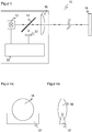
- FIG. 1 shows a schematic representation of an optoelectronic sensor 10.
- a light emitter 12 emits a light signal which passes through a splitter mirror 14 and is then guided by means of a lens 16 to an object 18. After remission or reflection, a portion of the light signal returns, is focused by the lens 16 and deflected by the splitter mirror 14 onto a light receiver 20.
- An evaluation unit 22 is connected to the light transmitter 12 and the light receiver 20. In this way, a desired light signal is generated by means of the light transmitter 12 and the reception signal subsequently generated by the light receiver 20 is evaluated in order, for example, to detect the presence of the object 18.
- the invention is not limited to a particular sensor type or a particular design. Rather, it is only important that at least one optical component is present, which, for correct functioning of the sensor, has an adjusted position and / or orientation relative to the sensor or to another optical component must have.
- These optical components can in the embodiment of the FIG. 1 the light emitter 10, the divider mirror 14, the lens 16 and / or the light receiver 20 may be.
- FIGS. 2 and 3 show the relevant manufacturing steps, with which the optical components are fixed with a 3D-printed optics carrier in the desired adjustment. Not all optical components need to be adjusted in this way. It is also conceivable to adjust some optical components in other ways, and again other optical components may not require adjustment or only a very rough adjustment.
- FIG. 2 shows a first of the respective manufacturing steps, in which two optical components, namely the light emitter 12 and the lens 16, are positioned to each other.
- the optical components are to be understood purely by way of example; likewise, the light receiver 20 could be positioned relative to the lens 16, two or more arbitrary optical components to one another or only one optical component to the optical carrier still to be created.
- the optical components 12, 16 to be aligned with one another are positioned freely in space with the aid of a positioning device 24a-b in such a way that the desired interaction results.
- a positioning device 24a-b In the illustrated example, one optical component 12 is held by a rigid part 24a of the positioning device and only the other optical component 16 is moved. This is then sufficient and simplifies the positioning 24a-b, if it only depends on the relative position of the optical components 12, 16 to each other.
- the solid part 24a may also be replaced to move both optical components 16.
- the movable part 24b of the positioning device is, for example, a robot arm, although other electrically adjustable or mechanical movements are also conceivable.
- the freedom of movement of the movable part 24b in all six degrees of freedom of translation and rotation is symbolized by an axis system 26. Often, only a portion of these degrees of freedom is actually needed, for example, only one degree of translation freedom on the axis between the optical components 12, 16 to adjust the spacing. That's enough then a correspondingly simplified movable part 24b of the positioning device.
- the receptacles of the positioning device 24a-b are very precise, so that it is sufficient to approach a predetermined fixed position.
- a form of feedback will also be incorporated. This can be a comparison with a target position by a camera or an operator. For very accurate alignment results, it is useful to enable the optical path to be set and see if the desired result is achieved.
- the light emitter 12 can be switched on and the light spot behind the lens 16 can be checked.
- the first production step is completed.
- FIG. 3 illustrates the subsequent second manufacturing step.
- the positioning device 24a-b remains in the previously reached position and thus keeps the optical components 12, 16 in the desired orientation.
- a 3D printer not shown, is constructed an optical carrier 28 around the optical components 12, 16, which fixes the optical components 12, 16 in the achieved alignment.
- the stripe pattern in FIG. 3 indicates a layer structure of the 3D printing process on a substrate 30, for example a workbench, but with which no special 3D printing process is to be defined.
- the optical components 12, 16 can be released by the positioning device 24a-b as soon as they are sufficiently fixed. It is conceivable only then complete the 3D printing, if this was previously not possible because of the gripping contact. In this case, there may be waiting times during the 3D printing or after that, so that the material of the optical carrier 28 cools or hardens.
- the 3D printing is not limited to the optical carrier 28 alone, but it can be a larger assembly with the optical carrier 28 or the entire housing to be printed. Of course, more or less than the two optical components 12, 16 shown by way of example may be held in an adjusted position. On the other hand, it is also possible to print only images for those components whose alignment can cope with the tolerances of 3D printing, and to subsequently use these components. Also, non-optical components can be integrated into the 3D printing, for example by connecting an electric motor, the fixation of whole electronic cards or other other sensor components.
- FIG. 4 illustrates a conceivable supporting measure for 3D printing. It is FIG. 4a a front view and FIG. 4b a section of the lens 16 as a naturally replaceable example of an optical component.
- the lens 16 is provided in this embodiment with "ears" or pads 32.
- the terminal areas 32 make it easier for the positioning device 24a-b to grip the lens 16 and fix it in the desired orientation during the 3D printing. In addition, they can provide better interfacing between the lens 16 and the printed optics carrier 28.
- the connection regions 32 can be made in one piece with the lens 16, for instance by injection molding, or the lens 16 is assembled with the connection region 32. In this case, no special precision is required, because it does not depend on the mutual alignment of the lens 16 and connection area 32, but on the effective orientation of the first yes with the help of the positioning device 24a-b freely positionable lens 16.
- the positioning device 24a-b forms, together with the 3D printer, a kind of universal station for the ready-to-use production of a wide variety of completely adjusted optical assemblies.
- a particular advantage is that the manufacturing process according to the invention with positioning and 3D printing can take place directly in the production line. This speeds up the production compared to a conventional, temporally upstream production of an optical carrier 28 quite considerably. In addition, it is very easy and inexpensive to ensure any desired orientation. In addition, the production line becomes highly flexible for a wide variety of sensor variants or even sensor types. This also small and small series or even individually specified sensors are economically produced. In addition, the process is suitable for prototyping and significantly accelerates the development and transition from development to mass production.
Landscapes
- Physics & Mathematics (AREA)
- Life Sciences & Earth Sciences (AREA)
- General Life Sciences & Earth Sciences (AREA)
- General Physics & Mathematics (AREA)
- Geophysics (AREA)
- Chemical & Material Sciences (AREA)
- Engineering & Computer Science (AREA)
- Manufacturing & Machinery (AREA)
- Materials Engineering (AREA)
- Switches Operated By Changes In Physical Conditions (AREA)
- Manufacture Of Switches (AREA)
Applications Claiming Priority (1)
| Application Number | Priority Date | Filing Date | Title |
|---|---|---|---|
| DE102016101928.3A DE102016101928A1 (de) | 2016-02-04 | 2016-02-04 | Optoelektronischer Sensor mit Verfahren zur Herstellung |
Publications (2)
| Publication Number | Publication Date |
|---|---|
| EP3202573A1 true EP3202573A1 (fr) | 2017-08-09 |
| EP3202573B1 EP3202573B1 (fr) | 2018-06-20 |
Family
ID=57838197
Family Applications (1)
| Application Number | Title | Priority Date | Filing Date |
|---|---|---|---|
| EP17151450.8A Active EP3202573B1 (fr) | 2016-02-04 | 2017-01-13 | Procédé de fabrication d'un capteur optoélectronique |
Country Status (3)
| Country | Link |
|---|---|
| EP (1) | EP3202573B1 (fr) |
| JP (1) | JP6602801B2 (fr) |
| DE (1) | DE102016101928A1 (fr) |
Cited By (1)
| Publication number | Priority date | Publication date | Assignee | Title |
|---|---|---|---|---|
| US11415893B2 (en) | 2017-10-30 | 2022-08-16 | Asml Holding N. V. | Assembly for use in semiconductor photolithography and method of manufacturing same |
Families Citing this family (1)
| Publication number | Priority date | Publication date | Assignee | Title |
|---|---|---|---|---|
| DE102023132805A1 (de) | 2023-11-24 | 2025-05-28 | Trioptics Gmbh | Optikelement zum Einsetzen in eine optische Vorrichtung, optische Vorrichtung, Verfahren zum Herstellen eines Optikelements und Verfahren zum Herstellen einer optischen Vorrichtung |
Citations (3)
| Publication number | Priority date | Publication date | Assignee | Title |
|---|---|---|---|---|
| US20130170171A1 (en) * | 2012-01-04 | 2013-07-04 | Board Of Regents, The University Of Texas System | Extrusion-based additive manufacturing system for 3d structural electronic, electromagnetic and electromechanical components/devices |
| US20140153087A1 (en) * | 2011-07-29 | 2014-06-05 | Gloucestershire Hospitals Nhs Foundation Trust | Optical Device |
| US20150167926A1 (en) * | 2013-12-16 | 2015-06-18 | Vode Lighting Llc | Lighting optics for luminaires |
Family Cites Families (4)
| Publication number | Priority date | Publication date | Assignee | Title |
|---|---|---|---|---|
| JP2000180686A (ja) * | 1998-12-18 | 2000-06-30 | Nec Corp | 光モジュール及び該光モジュールが具える光学部品の位置調整方法 |
| DE102008009680A1 (de) * | 2008-02-18 | 2009-08-27 | Siemens Aktiengesellschaft | Dreidimensionale Vermessung von Objekten mittels eines modular aufgebauten Triangulationssensors |
| JP5292131B2 (ja) * | 2009-02-27 | 2013-09-18 | パナソニック デバイスSunx株式会社 | 投光モジュールの製造方法、及び投光器 |
| DE202014103670U1 (de) * | 2014-08-06 | 2014-09-17 | Balluff Gmbh | Optoelektronischer Sensor |
-
2016
- 2016-02-04 DE DE102016101928.3A patent/DE102016101928A1/de not_active Withdrawn
-
2017
- 2017-01-13 EP EP17151450.8A patent/EP3202573B1/fr active Active
- 2017-02-01 JP JP2017016460A patent/JP6602801B2/ja active Active
Patent Citations (3)
| Publication number | Priority date | Publication date | Assignee | Title |
|---|---|---|---|---|
| US20140153087A1 (en) * | 2011-07-29 | 2014-06-05 | Gloucestershire Hospitals Nhs Foundation Trust | Optical Device |
| US20130170171A1 (en) * | 2012-01-04 | 2013-07-04 | Board Of Regents, The University Of Texas System | Extrusion-based additive manufacturing system for 3d structural electronic, electromagnetic and electromechanical components/devices |
| US20150167926A1 (en) * | 2013-12-16 | 2015-06-18 | Vode Lighting Llc | Lighting optics for luminaires |
Non-Patent Citations (2)
| Title |
|---|
| ALOK KATARIA ET AL: "Building around inserts: methods for fabricating complex devices in stereolithography", RAPID PROTOTYPING JOURNAL, 1 January 2001 (2001-01-01), pages 253 - 262, XP055376379, Retrieved from the Internet <URL:http://www.emeraldinsight.com/doi/pdfplus/10.1108/13552540110410459> [retrieved on 20170529] * |
| KARL WILLIS ET AL: "Printed optics", UIST '12,PROCEEDINGS OF THE ANNUAL ACM SYMPOSIUM ON USER INTERFACE SOFTWARE AND TECHNOLOGY, 1 January 2012 (2012-01-01), CAMBRIDGE, MASSACHUSETTS, USA, pages 589, XP055294374, ISBN: 978-1-4503-1580-7, DOI: 10.1145/2380116.2380190 * |
Cited By (1)
| Publication number | Priority date | Publication date | Assignee | Title |
|---|---|---|---|---|
| US11415893B2 (en) | 2017-10-30 | 2022-08-16 | Asml Holding N. V. | Assembly for use in semiconductor photolithography and method of manufacturing same |
Also Published As
| Publication number | Publication date |
|---|---|
| JP2017162796A (ja) | 2017-09-14 |
| DE102016101928A1 (de) | 2017-08-10 |
| EP3202573B1 (fr) | 2018-06-20 |
| JP6602801B2 (ja) | 2019-11-06 |
Similar Documents
| Publication | Publication Date | Title |
|---|---|---|
| DE2361155C2 (de) | Vorrichtung zum Positionieren eines ersten Gegenstandes in bezug auf einen zweiten Gegenstand | |
| DE3643252C2 (de) | Bestückungsautomat mit sensorgestützter Lagekorrekturvorrichtung | |
| EP1184640A2 (fr) | Dispositif de mesure de la géométrie d' un véhicule | |
| DE3650509T2 (de) | Zoom-Mikroskop mit Kurbel und Gestängemechanismus | |
| DE102017010055A1 (de) | Laserstrahlschweißen von geometrischen Figuren mit OCT-Nahtführung | |
| DE102013102819A1 (de) | Kameramodul sowie Verfahren zur Herstellung | |
| EP4242719A2 (fr) | Dispositif de reproduction multi-ouverture, système de reproduction et procédé de fourniture d'un dispositif de reproduction multi-ouverture | |
| WO2012013818A1 (fr) | Procédé et dispositif servant à calibrer une machine d'usinage au laser en utilisant un capteur de lumière laser | |
| DE102014104028A1 (de) | Optoelektronische Vorrichtung und Verfahren zum Justieren | |
| EP3202573B1 (fr) | Procédé de fabrication d'un capteur optoélectronique | |
| DE2202172C3 (de) | Anordnung zum automatischen Nachführen | |
| DD202074A5 (de) | Strahlenumlenkvorrichtung | |
| EP3020532A1 (fr) | Dispositif de soudage de matiere synthetique et procede de soudage de matiere synthetique associe | |
| DE69230222T2 (de) | Verfahren zur fixierung eines optischen bildsensors in ausrichtung zur bildfläche einer linsenanordnung | |
| DE2354338B2 (de) | Vorrichtung zur Montage einer aus Röhrensockel und vormontiertem Mehrstrahlsystem gebildeten Sockeleinheit am Kolben einer Kathodenstrahlröhre | |
| EP1091228A2 (fr) | Dispositif d'émission comprenant une fibre optique permettant un couplage précisément réglé | |
| DE3246220A1 (de) | Verfahren zum automatischen zuordnen und verbinden zweier koerper, insbesondere einer radfelge und einer radnabe | |
| DE4002370B4 (de) | Verfahren und Vorrichtung zum Justieren der optischen Kopplung von Lichtwellenleitern und optischen Bauelementen | |
| DE102015212123A1 (de) | Kameragehäuse zur Justierung einer Optik | |
| DE102017121454A1 (de) | Vorrichtung zur Justierung eines Polarisationsfilters sowie Herstellungsverfahren | |
| DE102016221734A1 (de) | Verfahren zur Feinausrichtung von Roboterwerkzeugen | |
| EP1082193A1 (fr) | Procede et dispositif pour la realisation d'etapes de travail sur des modules miniaturises | |
| DE202012101965U1 (de) | Stereokamera | |
| DE3307453C1 (de) | Verfahren zur koaxialen Kopplung zweier Fasern | |
| DE102019205042B4 (de) | Vorrichtung und Verfahren zur Positionierung eines Sensors oder Sensorteils |
Legal Events
| Date | Code | Title | Description |
|---|---|---|---|
| PUAI | Public reference made under article 153(3) epc to a published international application that has entered the european phase |
Free format text: ORIGINAL CODE: 0009012 |
|
| STAA | Information on the status of an ep patent application or granted ep patent |
Free format text: STATUS: THE APPLICATION HAS BEEN PUBLISHED |
|
| AK | Designated contracting states |
Kind code of ref document: A1 Designated state(s): AL AT BE BG CH CY CZ DE DK EE ES FI FR GB GR HR HU IE IS IT LI LT LU LV MC MK MT NL NO PL PT RO RS SE SI SK SM TR |
|
| AX | Request for extension of the european patent |
Extension state: BA ME |
|
| STAA | Information on the status of an ep patent application or granted ep patent |
Free format text: STATUS: REQUEST FOR EXAMINATION WAS MADE |
|
| 17P | Request for examination filed |
Effective date: 20170809 |
|
| RBV | Designated contracting states (corrected) |
Designated state(s): AL AT BE BG CH CY CZ DE DK EE ES FI FR GB GR HR HU IE IS IT LI LT LU LV MC MK MT NL NO PL PT RO RS SE SI SK SM TR |
|
| GRAP | Despatch of communication of intention to grant a patent |
Free format text: ORIGINAL CODE: EPIDOSNIGR1 |
|
| STAA | Information on the status of an ep patent application or granted ep patent |
Free format text: STATUS: GRANT OF PATENT IS INTENDED |
|
| INTG | Intention to grant announced |
Effective date: 20171219 |
|
| GRAS | Grant fee paid |
Free format text: ORIGINAL CODE: EPIDOSNIGR3 |
|
| GRAA | (expected) grant |
Free format text: ORIGINAL CODE: 0009210 |
|
| STAA | Information on the status of an ep patent application or granted ep patent |
Free format text: STATUS: THE PATENT HAS BEEN GRANTED |
|
| AK | Designated contracting states |
Kind code of ref document: B1 Designated state(s): AL AT BE BG CH CY CZ DE DK EE ES FI FR GB GR HR HU IE IS IT LI LT LU LV MC MK MT NL NO PL PT RO RS SE SI SK SM TR |
|
| REG | Reference to a national code |
Ref country code: GB Ref legal event code: FG4D Free format text: NOT ENGLISH |
|
| REG | Reference to a national code |
Ref country code: IE Ref legal event code: FG4D Free format text: LANGUAGE OF EP DOCUMENT: GERMAN |
|
| REG | Reference to a national code |
Ref country code: AT Ref legal event code: REF Ref document number: 1010288 Country of ref document: AT Kind code of ref document: T Effective date: 20180715 |
|
| REG | Reference to a national code |
Ref country code: DE Ref legal event code: R096 Ref document number: 502017000047 Country of ref document: DE |
|
| REG | Reference to a national code |
Ref country code: NL Ref legal event code: MP Effective date: 20180620 |
|
| PG25 | Lapsed in a contracting state [announced via postgrant information from national office to epo] |
Ref country code: NO Free format text: LAPSE BECAUSE OF FAILURE TO SUBMIT A TRANSLATION OF THE DESCRIPTION OR TO PAY THE FEE WITHIN THE PRESCRIBED TIME-LIMIT Effective date: 20180920 Ref country code: SE Free format text: LAPSE BECAUSE OF FAILURE TO SUBMIT A TRANSLATION OF THE DESCRIPTION OR TO PAY THE FEE WITHIN THE PRESCRIBED TIME-LIMIT Effective date: 20180620 Ref country code: FI Free format text: LAPSE BECAUSE OF FAILURE TO SUBMIT A TRANSLATION OF THE DESCRIPTION OR TO PAY THE FEE WITHIN THE PRESCRIBED TIME-LIMIT Effective date: 20180620 Ref country code: BG Free format text: LAPSE BECAUSE OF FAILURE TO SUBMIT A TRANSLATION OF THE DESCRIPTION OR TO PAY THE FEE WITHIN THE PRESCRIBED TIME-LIMIT Effective date: 20180920 Ref country code: LT Free format text: LAPSE BECAUSE OF FAILURE TO SUBMIT A TRANSLATION OF THE DESCRIPTION OR TO PAY THE FEE WITHIN THE PRESCRIBED TIME-LIMIT Effective date: 20180620 |
|
| REG | Reference to a national code |
Ref country code: LT Ref legal event code: MG4D |
|
| PG25 | Lapsed in a contracting state [announced via postgrant information from national office to epo] |
Ref country code: GR Free format text: LAPSE BECAUSE OF FAILURE TO SUBMIT A TRANSLATION OF THE DESCRIPTION OR TO PAY THE FEE WITHIN THE PRESCRIBED TIME-LIMIT Effective date: 20180921 Ref country code: LV Free format text: LAPSE BECAUSE OF FAILURE TO SUBMIT A TRANSLATION OF THE DESCRIPTION OR TO PAY THE FEE WITHIN THE PRESCRIBED TIME-LIMIT Effective date: 20180620 Ref country code: RS Free format text: LAPSE BECAUSE OF FAILURE TO SUBMIT A TRANSLATION OF THE DESCRIPTION OR TO PAY THE FEE WITHIN THE PRESCRIBED TIME-LIMIT Effective date: 20180620 Ref country code: HR Free format text: LAPSE BECAUSE OF FAILURE TO SUBMIT A TRANSLATION OF THE DESCRIPTION OR TO PAY THE FEE WITHIN THE PRESCRIBED TIME-LIMIT Effective date: 20180620 |
|
| PG25 | Lapsed in a contracting state [announced via postgrant information from national office to epo] |
Ref country code: NL Free format text: LAPSE BECAUSE OF FAILURE TO SUBMIT A TRANSLATION OF THE DESCRIPTION OR TO PAY THE FEE WITHIN THE PRESCRIBED TIME-LIMIT Effective date: 20180620 |
|
| PG25 | Lapsed in a contracting state [announced via postgrant information from national office to epo] |
Ref country code: PL Free format text: LAPSE BECAUSE OF FAILURE TO SUBMIT A TRANSLATION OF THE DESCRIPTION OR TO PAY THE FEE WITHIN THE PRESCRIBED TIME-LIMIT Effective date: 20180620 Ref country code: IS Free format text: LAPSE BECAUSE OF FAILURE TO SUBMIT A TRANSLATION OF THE DESCRIPTION OR TO PAY THE FEE WITHIN THE PRESCRIBED TIME-LIMIT Effective date: 20181020 Ref country code: EE Free format text: LAPSE BECAUSE OF FAILURE TO SUBMIT A TRANSLATION OF THE DESCRIPTION OR TO PAY THE FEE WITHIN THE PRESCRIBED TIME-LIMIT Effective date: 20180620 Ref country code: RO Free format text: LAPSE BECAUSE OF FAILURE TO SUBMIT A TRANSLATION OF THE DESCRIPTION OR TO PAY THE FEE WITHIN THE PRESCRIBED TIME-LIMIT Effective date: 20180620 Ref country code: CZ Free format text: LAPSE BECAUSE OF FAILURE TO SUBMIT A TRANSLATION OF THE DESCRIPTION OR TO PAY THE FEE WITHIN THE PRESCRIBED TIME-LIMIT Effective date: 20180620 Ref country code: SK Free format text: LAPSE BECAUSE OF FAILURE TO SUBMIT A TRANSLATION OF THE DESCRIPTION OR TO PAY THE FEE WITHIN THE PRESCRIBED TIME-LIMIT Effective date: 20180620 |
|
| PG25 | Lapsed in a contracting state [announced via postgrant information from national office to epo] |
Ref country code: IT Free format text: LAPSE BECAUSE OF FAILURE TO SUBMIT A TRANSLATION OF THE DESCRIPTION OR TO PAY THE FEE WITHIN THE PRESCRIBED TIME-LIMIT Effective date: 20180620 Ref country code: SM Free format text: LAPSE BECAUSE OF FAILURE TO SUBMIT A TRANSLATION OF THE DESCRIPTION OR TO PAY THE FEE WITHIN THE PRESCRIBED TIME-LIMIT Effective date: 20180620 Ref country code: ES Free format text: LAPSE BECAUSE OF FAILURE TO SUBMIT A TRANSLATION OF THE DESCRIPTION OR TO PAY THE FEE WITHIN THE PRESCRIBED TIME-LIMIT Effective date: 20180620 |
|
| REG | Reference to a national code |
Ref country code: DE Ref legal event code: R097 Ref document number: 502017000047 Country of ref document: DE |
|
| PLBE | No opposition filed within time limit |
Free format text: ORIGINAL CODE: 0009261 |
|
| STAA | Information on the status of an ep patent application or granted ep patent |
Free format text: STATUS: NO OPPOSITION FILED WITHIN TIME LIMIT |
|
| 26N | No opposition filed |
Effective date: 20190321 |
|
| PG25 | Lapsed in a contracting state [announced via postgrant information from national office to epo] |
Ref country code: DK Free format text: LAPSE BECAUSE OF FAILURE TO SUBMIT A TRANSLATION OF THE DESCRIPTION OR TO PAY THE FEE WITHIN THE PRESCRIBED TIME-LIMIT Effective date: 20180620 |
|
| PG25 | Lapsed in a contracting state [announced via postgrant information from national office to epo] |
Ref country code: MC Free format text: LAPSE BECAUSE OF FAILURE TO SUBMIT A TRANSLATION OF THE DESCRIPTION OR TO PAY THE FEE WITHIN THE PRESCRIBED TIME-LIMIT Effective date: 20180620 Ref country code: SI Free format text: LAPSE BECAUSE OF FAILURE TO SUBMIT A TRANSLATION OF THE DESCRIPTION OR TO PAY THE FEE WITHIN THE PRESCRIBED TIME-LIMIT Effective date: 20180620 |
|
| PG25 | Lapsed in a contracting state [announced via postgrant information from national office to epo] |
Ref country code: LU Free format text: LAPSE BECAUSE OF NON-PAYMENT OF DUE FEES Effective date: 20190113 |
|
| REG | Reference to a national code |
Ref country code: BE Ref legal event code: MM Effective date: 20190131 |
|
| REG | Reference to a national code |
Ref country code: IE Ref legal event code: MM4A |
|
| PG25 | Lapsed in a contracting state [announced via postgrant information from national office to epo] |
Ref country code: BE Free format text: LAPSE BECAUSE OF NON-PAYMENT OF DUE FEES Effective date: 20190131 Ref country code: AL Free format text: LAPSE BECAUSE OF FAILURE TO SUBMIT A TRANSLATION OF THE DESCRIPTION OR TO PAY THE FEE WITHIN THE PRESCRIBED TIME-LIMIT Effective date: 20180620 |
|
| PG25 | Lapsed in a contracting state [announced via postgrant information from national office to epo] |
Ref country code: IE Free format text: LAPSE BECAUSE OF NON-PAYMENT OF DUE FEES Effective date: 20190113 |
|
| PG25 | Lapsed in a contracting state [announced via postgrant information from national office to epo] |
Ref country code: TR Free format text: LAPSE BECAUSE OF FAILURE TO SUBMIT A TRANSLATION OF THE DESCRIPTION OR TO PAY THE FEE WITHIN THE PRESCRIBED TIME-LIMIT Effective date: 20180620 |
|
| PG25 | Lapsed in a contracting state [announced via postgrant information from national office to epo] |
Ref country code: MT Free format text: LAPSE BECAUSE OF FAILURE TO SUBMIT A TRANSLATION OF THE DESCRIPTION OR TO PAY THE FEE WITHIN THE PRESCRIBED TIME-LIMIT Effective date: 20180620 Ref country code: PT Free format text: LAPSE BECAUSE OF FAILURE TO SUBMIT A TRANSLATION OF THE DESCRIPTION OR TO PAY THE FEE WITHIN THE PRESCRIBED TIME-LIMIT Effective date: 20181022 |
|
| PG25 | Lapsed in a contracting state [announced via postgrant information from national office to epo] |
Ref country code: CY Free format text: LAPSE BECAUSE OF FAILURE TO SUBMIT A TRANSLATION OF THE DESCRIPTION OR TO PAY THE FEE WITHIN THE PRESCRIBED TIME-LIMIT Effective date: 20180620 |
|
| PG25 | Lapsed in a contracting state [announced via postgrant information from national office to epo] |
Ref country code: HU Free format text: LAPSE BECAUSE OF FAILURE TO SUBMIT A TRANSLATION OF THE DESCRIPTION OR TO PAY THE FEE WITHIN THE PRESCRIBED TIME-LIMIT; INVALID AB INITIO Effective date: 20170113 |
|
| GBPC | Gb: european patent ceased through non-payment of renewal fee |
Effective date: 20210113 |
|
| PG25 | Lapsed in a contracting state [announced via postgrant information from national office to epo] |
Ref country code: GB Free format text: LAPSE BECAUSE OF NON-PAYMENT OF DUE FEES Effective date: 20210113 |
|
| PG25 | Lapsed in a contracting state [announced via postgrant information from national office to epo] |
Ref country code: MK Free format text: LAPSE BECAUSE OF FAILURE TO SUBMIT A TRANSLATION OF THE DESCRIPTION OR TO PAY THE FEE WITHIN THE PRESCRIBED TIME-LIMIT Effective date: 20180620 |
|
| PGFP | Annual fee paid to national office [announced via postgrant information from national office to epo] |
Ref country code: CH Payment date: 20250201 Year of fee payment: 9 Ref country code: AT Payment date: 20250120 Year of fee payment: 9 |
|
| PGFP | Annual fee paid to national office [announced via postgrant information from national office to epo] |
Ref country code: DE Payment date: 20260120 Year of fee payment: 10 |
|
| PGFP | Annual fee paid to national office [announced via postgrant information from national office to epo] |
Ref country code: FR Payment date: 20260127 Year of fee payment: 10 |