EP3206464B1 - Procédé de fabrication d'un module lumineux d'un dispositif d'éclairage de véhicule automobile - Google Patents
Procédé de fabrication d'un module lumineux d'un dispositif d'éclairage de véhicule automobile Download PDFInfo
- Publication number
- EP3206464B1 EP3206464B1 EP17155567.5A EP17155567A EP3206464B1 EP 3206464 B1 EP3206464 B1 EP 3206464B1 EP 17155567 A EP17155567 A EP 17155567A EP 3206464 B1 EP3206464 B1 EP 3206464B1
- Authority
- EP
- European Patent Office
- Prior art keywords
- circuit board
- light
- hole
- offset
- pattern
- Prior art date
- Legal status (The legal status is an assumption and is not a legal conclusion. Google has not performed a legal analysis and makes no representation as to the accuracy of the status listed.)
- Active
Links
Images

Classifications
-
- H—ELECTRICITY
- H05—ELECTRIC TECHNIQUES NOT OTHERWISE PROVIDED FOR
- H05K—PRINTED CIRCUITS; CASINGS OR CONSTRUCTIONAL DETAILS OF ELECTRIC APPARATUS; MANUFACTURE OF ASSEMBLAGES OF ELECTRICAL COMPONENTS
- H05K3/00—Apparatus or processes for manufacturing printed circuits
- H05K3/30—Assembling printed circuits with electric components, e.g. with resistors
- H05K3/32—Assembling printed circuits with electric components, e.g. with resistors electrically connecting electric components or wires to printed circuits
- H05K3/34—Assembling printed circuits with electric components, e.g. with resistors electrically connecting electric components or wires to printed circuits by soldering
- H05K3/341—Surface mounted components
- H05K3/3431—Leadless components
-
- F—MECHANICAL ENGINEERING; LIGHTING; HEATING; WEAPONS; BLASTING
- F21—LIGHTING
- F21S—NON-PORTABLE LIGHTING DEVICES; SYSTEMS THEREOF; VEHICLE LIGHTING DEVICES SPECIALLY ADAPTED FOR VEHICLE EXTERIORS
- F21S41/00—Illuminating devices specially adapted for vehicle exteriors, e.g. headlamps
- F21S41/10—Illuminating devices specially adapted for vehicle exteriors, e.g. headlamps characterised by the light source
- F21S41/14—Illuminating devices specially adapted for vehicle exteriors, e.g. headlamps characterised by the light source characterised by the type of light source
- F21S41/141—Light emitting diodes [LED]
- F21S41/147—Light emitting diodes [LED] the main emission direction of the LED being angled to the optical axis of the illuminating device
-
- F—MECHANICAL ENGINEERING; LIGHTING; HEATING; WEAPONS; BLASTING
- F21—LIGHTING
- F21S—NON-PORTABLE LIGHTING DEVICES; SYSTEMS THEREOF; VEHICLE LIGHTING DEVICES SPECIALLY ADAPTED FOR VEHICLE EXTERIORS
- F21S41/00—Illuminating devices specially adapted for vehicle exteriors, e.g. headlamps
- F21S41/10—Illuminating devices specially adapted for vehicle exteriors, e.g. headlamps characterised by the light source
- F21S41/14—Illuminating devices specially adapted for vehicle exteriors, e.g. headlamps characterised by the light source characterised by the type of light source
- F21S41/141—Light emitting diodes [LED]
- F21S41/151—Light emitting diodes [LED] arranged in one or more lines
-
- F—MECHANICAL ENGINEERING; LIGHTING; HEATING; WEAPONS; BLASTING
- F21—LIGHTING
- F21S—NON-PORTABLE LIGHTING DEVICES; SYSTEMS THEREOF; VEHICLE LIGHTING DEVICES SPECIALLY ADAPTED FOR VEHICLE EXTERIORS
- F21S41/00—Illuminating devices specially adapted for vehicle exteriors, e.g. headlamps
- F21S41/10—Illuminating devices specially adapted for vehicle exteriors, e.g. headlamps characterised by the light source
- F21S41/14—Illuminating devices specially adapted for vehicle exteriors, e.g. headlamps characterised by the light source characterised by the type of light source
- F21S41/141—Light emitting diodes [LED]
- F21S41/151—Light emitting diodes [LED] arranged in one or more lines
- F21S41/153—Light emitting diodes [LED] arranged in one or more lines arranged in a matrix
-
- F—MECHANICAL ENGINEERING; LIGHTING; HEATING; WEAPONS; BLASTING
- F21—LIGHTING
- F21S—NON-PORTABLE LIGHTING DEVICES; SYSTEMS THEREOF; VEHICLE LIGHTING DEVICES SPECIALLY ADAPTED FOR VEHICLE EXTERIORS
- F21S41/00—Illuminating devices specially adapted for vehicle exteriors, e.g. headlamps
- F21S41/10—Illuminating devices specially adapted for vehicle exteriors, e.g. headlamps characterised by the light source
- F21S41/19—Attachment of light sources or lamp holders
- F21S41/192—Details of lamp holders, terminals or connectors
-
- F—MECHANICAL ENGINEERING; LIGHTING; HEATING; WEAPONS; BLASTING
- F21—LIGHTING
- F21S—NON-PORTABLE LIGHTING DEVICES; SYSTEMS THEREOF; VEHICLE LIGHTING DEVICES SPECIALLY ADAPTED FOR VEHICLE EXTERIORS
- F21S41/00—Illuminating devices specially adapted for vehicle exteriors, e.g. headlamps
- F21S41/20—Illuminating devices specially adapted for vehicle exteriors, e.g. headlamps characterised by refractors, transparent cover plates, light guides or filters
- F21S41/29—Attachment thereof
-
- F—MECHANICAL ENGINEERING; LIGHTING; HEATING; WEAPONS; BLASTING
- F21—LIGHTING
- F21S—NON-PORTABLE LIGHTING DEVICES; SYSTEMS THEREOF; VEHICLE LIGHTING DEVICES SPECIALLY ADAPTED FOR VEHICLE EXTERIORS
- F21S41/00—Illuminating devices specially adapted for vehicle exteriors, e.g. headlamps
- F21S41/30—Illuminating devices specially adapted for vehicle exteriors, e.g. headlamps characterised by reflectors
- F21S41/32—Optical layout thereof
- F21S41/33—Multi-surface reflectors, e.g. reflectors with facets or reflectors with portions of different curvature
- F21S41/334—Multi-surface reflectors, e.g. reflectors with facets or reflectors with portions of different curvature the reflector consisting of patch like sectors
- F21S41/336—Multi-surface reflectors, e.g. reflectors with facets or reflectors with portions of different curvature the reflector consisting of patch like sectors with discontinuity at the junction between adjacent areas
-
- F—MECHANICAL ENGINEERING; LIGHTING; HEATING; WEAPONS; BLASTING
- F21—LIGHTING
- F21S—NON-PORTABLE LIGHTING DEVICES; SYSTEMS THEREOF; VEHICLE LIGHTING DEVICES SPECIALLY ADAPTED FOR VEHICLE EXTERIORS
- F21S41/00—Illuminating devices specially adapted for vehicle exteriors, e.g. headlamps
- F21S41/60—Illuminating devices specially adapted for vehicle exteriors, e.g. headlamps characterised by a variable light distribution
- F21S41/65—Illuminating devices specially adapted for vehicle exteriors, e.g. headlamps characterised by a variable light distribution by acting on light sources
- F21S41/663—Illuminating devices specially adapted for vehicle exteriors, e.g. headlamps characterised by a variable light distribution by acting on light sources by switching light sources
-
- G—PHYSICS
- G02—OPTICS
- G02B—OPTICAL ELEMENTS, SYSTEMS OR APPARATUS
- G02B19/00—Condensers, e.g. light collectors or similar non-imaging optics
- G02B19/0004—Condensers, e.g. light collectors or similar non-imaging optics characterised by the optical means employed
- G02B19/0009—Condensers, e.g. light collectors or similar non-imaging optics characterised by the optical means employed having refractive surfaces only
- G02B19/0014—Condensers, e.g. light collectors or similar non-imaging optics characterised by the optical means employed having refractive surfaces only at least one surface having optical power
-
- G—PHYSICS
- G02—OPTICS
- G02B—OPTICAL ELEMENTS, SYSTEMS OR APPARATUS
- G02B19/00—Condensers, e.g. light collectors or similar non-imaging optics
- G02B19/0033—Condensers, e.g. light collectors or similar non-imaging optics characterised by the use
- G02B19/0047—Condensers, e.g. light collectors or similar non-imaging optics characterised by the use for use with a light source
- G02B19/0061—Condensers, e.g. light collectors or similar non-imaging optics characterised by the use for use with a light source the light source comprising a LED
- G02B19/0066—Condensers, e.g. light collectors or similar non-imaging optics characterised by the use for use with a light source the light source comprising a LED in the form of an LED array
-
- G—PHYSICS
- G02—OPTICS
- G02B—OPTICAL ELEMENTS, SYSTEMS OR APPARATUS
- G02B3/00—Simple or compound lenses
- G02B3/02—Simple or compound lenses with non-spherical faces
- G02B3/08—Simple or compound lenses with non-spherical faces with discontinuous faces, e.g. Fresnel lens
-
- H—ELECTRICITY
- H05—ELECTRIC TECHNIQUES NOT OTHERWISE PROVIDED FOR
- H05K—PRINTED CIRCUITS; CASINGS OR CONSTRUCTIONAL DETAILS OF ELECTRIC APPARATUS; MANUFACTURE OF ASSEMBLAGES OF ELECTRICAL COMPONENTS
- H05K1/00—Printed circuits
- H05K1/02—Details
- H05K1/0266—Marks, test patterns or identification means
- H05K1/0269—Marks, test patterns or identification means for visual or optical inspection
-
- H—ELECTRICITY
- H05—ELECTRIC TECHNIQUES NOT OTHERWISE PROVIDED FOR
- H05K—PRINTED CIRCUITS; CASINGS OR CONSTRUCTIONAL DETAILS OF ELECTRIC APPARATUS; MANUFACTURE OF ASSEMBLAGES OF ELECTRICAL COMPONENTS
- H05K1/00—Printed circuits
- H05K1/02—Details
- H05K1/0274—Optical details, e.g. printed circuits comprising integral optical means
-
- H—ELECTRICITY
- H05—ELECTRIC TECHNIQUES NOT OTHERWISE PROVIDED FOR
- H05K—PRINTED CIRCUITS; CASINGS OR CONSTRUCTIONAL DETAILS OF ELECTRIC APPARATUS; MANUFACTURE OF ASSEMBLAGES OF ELECTRICAL COMPONENTS
- H05K3/00—Apparatus or processes for manufacturing printed circuits
- H05K3/0011—Working of insulating substrates or insulating layers
- H05K3/0044—Mechanical working of the substrate, e.g. drilling or punching
- H05K3/0047—Drilling of holes
-
- F—MECHANICAL ENGINEERING; LIGHTING; HEATING; WEAPONS; BLASTING
- F21—LIGHTING
- F21S—NON-PORTABLE LIGHTING DEVICES; SYSTEMS THEREOF; VEHICLE LIGHTING DEVICES SPECIALLY ADAPTED FOR VEHICLE EXTERIORS
- F21S41/00—Illuminating devices specially adapted for vehicle exteriors, e.g. headlamps
- F21S41/20—Illuminating devices specially adapted for vehicle exteriors, e.g. headlamps characterised by refractors, transparent cover plates, light guides or filters
- F21S41/285—Refractors, transparent cover plates, light guides or filters not provided in groups F21S41/24 - F21S41/2805
-
- F—MECHANICAL ENGINEERING; LIGHTING; HEATING; WEAPONS; BLASTING
- F21—LIGHTING
- F21S—NON-PORTABLE LIGHTING DEVICES; SYSTEMS THEREOF; VEHICLE LIGHTING DEVICES SPECIALLY ADAPTED FOR VEHICLE EXTERIORS
- F21S45/00—Arrangements within vehicle lighting devices specially adapted for vehicle exteriors, for purposes other than emission or distribution of light
- F21S45/40—Cooling of lighting devices
- F21S45/47—Passive cooling, e.g. using fins, thermal conductive elements or openings
-
- F—MECHANICAL ENGINEERING; LIGHTING; HEATING; WEAPONS; BLASTING
- F21—LIGHTING
- F21Y—INDEXING SCHEME ASSOCIATED WITH SUBCLASSES F21K, F21L, F21S and F21V, RELATING TO THE FORM OR THE KIND OF THE LIGHT SOURCES OR OF THE COLOUR OF THE LIGHT EMITTED
- F21Y2103/00—Elongate light sources, e.g. fluorescent tubes
- F21Y2103/10—Elongate light sources, e.g. fluorescent tubes comprising a linear array of point-like light-generating elements
-
- H—ELECTRICITY
- H05—ELECTRIC TECHNIQUES NOT OTHERWISE PROVIDED FOR
- H05K—PRINTED CIRCUITS; CASINGS OR CONSTRUCTIONAL DETAILS OF ELECTRIC APPARATUS; MANUFACTURE OF ASSEMBLAGES OF ELECTRICAL COMPONENTS
- H05K2201/00—Indexing scheme relating to printed circuits covered by H05K1/00
- H05K2201/09—Shape and layout
- H05K2201/09009—Substrate related
- H05K2201/09063—Holes or slots in insulating substrate not used for electrical connections
-
- H—ELECTRICITY
- H05—ELECTRIC TECHNIQUES NOT OTHERWISE PROVIDED FOR
- H05K—PRINTED CIRCUITS; CASINGS OR CONSTRUCTIONAL DETAILS OF ELECTRIC APPARATUS; MANUFACTURE OF ASSEMBLAGES OF ELECTRICAL COMPONENTS
- H05K2201/00—Indexing scheme relating to printed circuits covered by H05K1/00
- H05K2201/09—Shape and layout
- H05K2201/09209—Shape and layout details of conductors
- H05K2201/09654—Shape and layout details of conductors covering at least two types of conductors provided for in H05K2201/09218 - H05K2201/095
- H05K2201/09781—Dummy conductors, i.e. not used for normal transport of current; Dummy electrodes of components
-
- H—ELECTRICITY
- H05—ELECTRIC TECHNIQUES NOT OTHERWISE PROVIDED FOR
- H05K—PRINTED CIRCUITS; CASINGS OR CONSTRUCTIONAL DETAILS OF ELECTRIC APPARATUS; MANUFACTURE OF ASSEMBLAGES OF ELECTRICAL COMPONENTS
- H05K2201/00—Indexing scheme relating to printed circuits covered by H05K1/00
- H05K2201/09—Shape and layout
- H05K2201/09818—Shape or layout details not covered by a single group of H05K2201/09009 - H05K2201/09809
- H05K2201/09918—Optically detected marks used for aligning tool relative to the PCB, e.g. for mounting of components
-
- H—ELECTRICITY
- H05—ELECTRIC TECHNIQUES NOT OTHERWISE PROVIDED FOR
- H05K—PRINTED CIRCUITS; CASINGS OR CONSTRUCTIONAL DETAILS OF ELECTRIC APPARATUS; MANUFACTURE OF ASSEMBLAGES OF ELECTRICAL COMPONENTS
- H05K2201/00—Indexing scheme relating to printed circuits covered by H05K1/00
- H05K2201/10—Details of components or other objects attached to or integrated in a printed circuit board
- H05K2201/10007—Types of components
- H05K2201/10106—Light emitting diode [LED]
-
- H—ELECTRICITY
- H05—ELECTRIC TECHNIQUES NOT OTHERWISE PROVIDED FOR
- H05K—PRINTED CIRCUITS; CASINGS OR CONSTRUCTIONAL DETAILS OF ELECTRIC APPARATUS; MANUFACTURE OF ASSEMBLAGES OF ELECTRICAL COMPONENTS
- H05K2201/00—Indexing scheme relating to printed circuits covered by H05K1/00
- H05K2201/10—Details of components or other objects attached to or integrated in a printed circuit board
- H05K2201/10007—Types of components
- H05K2201/10121—Optical component, e.g. opto-electronic component
-
- H—ELECTRICITY
- H05—ELECTRIC TECHNIQUES NOT OTHERWISE PROVIDED FOR
- H05K—PRINTED CIRCUITS; CASINGS OR CONSTRUCTIONAL DETAILS OF ELECTRIC APPARATUS; MANUFACTURE OF ASSEMBLAGES OF ELECTRICAL COMPONENTS
- H05K2203/00—Indexing scheme relating to apparatus or processes for manufacturing printed circuits covered by H05K3/00
- H05K2203/16—Inspection; Monitoring; Aligning
- H05K2203/166—Alignment or registration; Control of registration
-
- Y—GENERAL TAGGING OF NEW TECHNOLOGICAL DEVELOPMENTS; GENERAL TAGGING OF CROSS-SECTIONAL TECHNOLOGIES SPANNING OVER SEVERAL SECTIONS OF THE IPC; TECHNICAL SUBJECTS COVERED BY FORMER USPC CROSS-REFERENCE ART COLLECTIONS [XRACs] AND DIGESTS
- Y02—TECHNOLOGIES OR APPLICATIONS FOR MITIGATION OR ADAPTATION AGAINST CLIMATE CHANGE
- Y02P—CLIMATE CHANGE MITIGATION TECHNOLOGIES IN THE PRODUCTION OR PROCESSING OF GOODS
- Y02P70/00—Climate change mitigation technologies in the production process for final industrial or consumer products
- Y02P70/50—Manufacturing or production processes characterised by the final manufactured product
Definitions
- the invention relates to a method for producing a light module of a motor vehicle lighting device according to the preamble of claim 1 and a light module of a motor vehicle lighting device according to the preamble of a subordinate claim.
- semiconductor light source components are assembled based on the conductor pattern, whereas optical components such as reflectors are mechanically aligned or attached to a circuit board directly or indirectly by means of holes drilled into a circuit board.
- optical components such as reflectors are mechanically aligned or attached to a circuit board directly or indirectly by means of holes drilled into a circuit board.
- the semiconductor light source component is not connected to the circuit board in the position that is necessary for the exact alignment of the semiconductor light source and reflector.
- WO2015000894A1 discloses a method for assembling electronic circuit boards with optical components, whereby the optical components are measured and positioned using image processing systems, with the following process steps: - the optical components are measured before the actual assembly process, preferably in the feed belt and the position of the optically relevant elements in Reference to the overall component is determined and a first correction factor is calculated from this, - from in the circuit board existing reference points for further optical components, at least one further correction factor is calculated, - during the assembly process, the specified installation positions are corrected with the correction factors and an actual installation position is determined, - the optical components are placed at the actual installation position. This enables precise positioning of the optical components relative to one another.
- DE4306998A1 discloses that a reference mark on a printed circuit board is detected in its image to determine points, thereby determining the preliminary center and diameter of the mark by a four-point search method.
- EP2722900A1 discloses a light source circuit unit that improves light extraction efficiency, and a lighting device and a display including such a light source circuit unit.
- the light source circuit unit includes: a circuit substrate having a wiring pattern on a surface thereof, the wiring pattern having light reflectivity, a circular base provided on the circuit substrate, a water-repellent portion provided from at least a peripheral edge portion of the base to a part of a side surface of the base and one or two or more light emitting device chips mounted on the socket and driven by a current flowing through the wiring pattern.
- US2015228549A1 discloses a method for constructing an LED light module, with a circuit board on which at least one LED lamp is accommodated, and with at least one optical element into which the light generated by the LED lamp can be emitted, the optical element having mounting pins and holes being formed in the circuit board so that the optical element is arranged by inserting the mounting pins into the holes on the circuit board , wherein the method comprises at least the following steps: arranging at least one LED lamp on a mounting surface of the circuit board, measuring the position of the LED lamp in the plane of the mounting surface of the circuit board, creating the holes in the circuit board at a position that is from the measured position of the LED lamp in the plane of the mounting surface, and arranging the optical element on the circuit board by inserting the mounting pins into the holes.
- DE102005033709A1 discloses a light-emitting module with a light source, a carrier for the light source and an optical element, the optical element having dowel pins which engage in corresponding recesses in the carrier.
- the light-emitting module is particularly suitable for use in optical projection devices and in vehicle headlights.
- the object of the invention is therefore to increase the accuracy of the optical imaging of a motor vehicle lighting device.
- an offset and/or a rotation between a conductor pattern and a drilling pattern of the circuit board is determined.
- the optical component is arranged on the circuit board depending on the offset and/or twist.
- the reference hole and a fastening hole for connecting the circuit board to the optical component are made using the same drilling program.
- tolerance differences between different drilling steps can be advantageously prevented Offset of the drilling pattern can be used for all further process steps through the reference drilling.
- the reference hole is arranged in the area of the registration mark, which advantageously enables the offset between the hole pattern and the conductor pattern to be detected by AOI.
- Figure 1 shows a light module 1 with several semiconductor light sources for emitting light, which are combined according to a light source arrangement 2.
- the light source arrangement 2 is arranged on a heat sink 3, although embodiments without the heat sink 3 are also conceivable.
- several semiconductor light sources can also be arranged in a row one above the other in a matrix-like manner.
- a primary optical element 17 is assigned to the semiconductor light sources to bundle at least part of the light emitted by the semiconductor light sources and to generate an intermediate light distribution.
- the primary optical element 17 comprises, for example, several primary optical elements, each for one semiconductor light source.
- the primary optical element 17 can also be referred to as an optical attachment or as an optical component.
- the intermediate light distributions are generated on light exit surfaces of the primary optical element 17.
- the intermediate light distributions are imaged by a secondary optics system 4 on a road in front of a motor vehicle as individual light distributions 6 'to produce a resulting overall light distribution 5 of the light module 1.
- the secondary optical system 4 is designed as a horizontally faceted reflector, in particular a parabolic reflector.
- a sagittal plane 8 has a substantially horizontal surface extent and includes the optical axis 7.
- a meridional plane 9 has a substantially vertical extent and also includes the optical axis 7.
- An intersection line between the sagittal plane 8 and the measuring screen 6 forms a horizontal HH 10 and a
- the intersection line between the meridional plane 9 and the measuring screen 6 forms a vertical W 11.
- the optical axis 7 runs through the intersection HV of the horizontal 10 and the vertical 11.
- the resulting overall light distribution 5 extends both below the horizontal 10 and above the horizontal 10.
- the overall light distribution 5 can be, for example, a so-called matrix high beam or a so-called strip high beam or a part thereof.
- the overall light distribution 5 can also form a particularly brightly illuminated central area of the high beam, a so-called high beam spot.
- a focal point of the faceted parabolic reflector 4 is designated by the reference number 12.
- a beam path of a main beam is designated by reference number 13 and the beam path of a secondary beam is designated by reference number 14.
- the main beam 13 results from a light beam emitted essentially in the main emission direction of one of the light sources, by shaping and possibly deflection by the primary optical element 17 assigned to the light source and by deflection on the secondary optical system 4.
- the secondary beam 14 is accordingly produced by one emitted obliquely to the main emission direction beam of light.
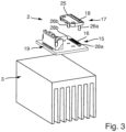
- Figure 2 shows a top view of the light source arrangement 2, which includes a plurality of light-emitting components 16, in particular semiconductor light sources.
- the light-emitting components 16 are arranged on a circuit board 19.
- light-emitting components 16 are designed as SMD LEDs (Surface Mounted Device-Light Emitting Diode).
- the circuit board 2 is arranged on the heat sink 3.
- the primary optical element 17 is arranged above the light-emitting components 16.
- the primary optical element 17 can also be referred to as an optical element that interacts optically with the light-emitting components 16.
- a reflector which is also referred to as an optical component, can also be connected to the circuit board 19.
- the circuit board 19 includes a registration mark 20, which in the present case is composed of two concentric circles 21 and 22.
- the two concentric circles 21 and 22, which are formed in the copper image of the circuit board 19, have a common circle center, which is referred to as the first position 24.
- additional registration marks 20 can of course also be arranged on the circuit board 19.
- the registration mark 20 can of course also have a different appearance in the form of other geometries.
- two through holes 26a and 26b are shown, for example for fastening the heat sink 3.
- Figure 3 shows an exploded view of the in Figure 2 top view shown.
- the primary optical element 17 has converging lenses 18 which include corresponding light exit surfaces 25. Furthermore, the primary optical element 17 has projections 26 which are intended to engage in bores 28. Of course, instead of the projections 26, another fastening device can also be used. or connecting means for connecting the primary optical element 17 and the circuit board 19 can be selected.
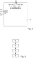
- Figure 4 shows in schematic form the top view of a circuit board 19 according to a method that is not part of the invention.
- the holes 28 are each carried out at a second position 30.
- dowel pins or plug-in pins can be inserted through the bores 28, which can each be designated as reference bores, which in turn engage in corresponding bores in the primary optical element 17.
- the plug-in pin is particularly suitable for use in an automatic assembly process.
- several holes 28 can also be provided.
- the hole 28 can also be referred to as a fastening hole.
- more than the one registration mark 20 shown can also be arranged on the circuit board 19. Two or three registration marks 20 are preferably arranged on the circuit board 19.
- Figure 5 shows a schematic flow diagram for the arrangement of the optical component 17 on the circuit board 19 Figure 4 according to the method not belonging to the invention.
- a first step 32 the circuit board 19 is manufactured. Inherent in circuit board production is a possible offset between a conductor pattern and a drilling pattern, which is why the hole 28 is only carried out in a step 36 after the circuit board production has been completed.
- the second position 30 is determined as a function of the first position 24.
- the hole 28 is carried out through the circuit board 19.
- a fourth step 38 following the third step 36 the optical component 17 is fixed to the circuit board 19, where In addition to a dowel pin or a plug-in pin, for example, other fastening means, in particular a screw, can also be used for the additional connection between the optical component 17 and the circuit board 19.
- the circuit board 19 can be fitted with the light-emitting components 16 between steps 32 and 34 and steps 36 and 38.
- the possible offset between the drilling pattern and the copper pattern of the circuit board 19 is compensated for by the arrangement of the hole 28 depending on the position 24, i.e. depending on the copper pattern.
- the optical component 17 for example from one of the Figures 2 and 3 depending on the first position 24 at least one registration mark and depending on a second position 30 at least one hole 28 connected through the circuit board 19 to the circuit board 19.
- the arrangement of the light-emitting component 16 and the drilling of the hole 28 through the circuit board 19 are each carried out depending on the registration mark 20.
- the primary optical element 17 is fixed to the circuit board 19 by means of the bore 28 and a fastening element arranged therein, such as a dowel pin or a plug-in pin.
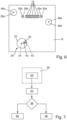
- Figure 6 shows a schematic top view of the circuit board 19 according to an exemplary embodiment of the method according to the invention.
- the holes 28 are not referred to as the reference hole, but rather a further hole 40 is referred to as the reference hole.
- the reference hole 40 is carried out during circuit board production together with the holes 26 and 28 using a single drilling program.
- the circuit board 19 according to Figure 6 further shows the Registration mark 20 with the first position 24. In the present case, the registration mark 20 only has a circle 22 and, together with the reference bore 40, is shown exaggeratedly large for graphical reasons. Two or three registration marks 20 are preferably arranged on the circuit board 19.
- the drilling program for arranging the reference hole 40 is programmed so that the first position 24 for the reference hole 40 is used as the target coordinate. If there is a difference between the holes 26, 28 and 40 carried out by the drilling program and the conductor pattern, an offset 42 appears between the first position 24 of the registration mark 20 and the position 44 of the reference hole 40, with the position 44 also being the second position is referred to in this context. The offset 42 and thus the positions 24 and 44 are only shown as examples. If the positions between the conductor pattern and the drilling pattern match, the second position 44 is located exactly above the first position 24.
- the holes 28 are offset by the offset 42 compared to the copper image. Accordingly, the light-emitting components 16 are placed by the offset 42 compared to the target position during assembly. The soldering pads for the components 16 are correspondingly larger so that contact is ensured in the event of an offset. Positions 46 of the holes 26 are marked by the offset 42 by the drilling program with which the holes 28 and 40 are also carried out and are part of the drilling pattern.
- the circuit board In a form not shown there are 19 on the circuit board several registration marks 20, in particular at least three registration marks 20, are arranged, with a reference bore 40 being carried out in at least one of the registration marks 20.
- the offset 42 can be determined more precisely, whereby in addition to the offset, a rotation of the hole pattern relative to the conductor pattern can also be recognized.
- registration marks 20 A variety of geometries of the copper layer are suitable as registration marks 20, which can be reliably detected using an optical inspection system.
- the ones in the Figures 5 and 6 The registration marks 20 shown can therefore also be designed differently and, for example, contain other geometric shapes such as crosses, circles or the like.
- the registration marks 20 should not be covered with solder paste or solder mask during circuit board production.
- An advantageous geometry for the registration mark 20 is a single ring in the copper layer of the circuit board 19, in the center of which there are essentially no further copper structures.
- the through hole 40 is preferably created within this annular structure of the registration mark 20.
- Figure 7 shows a schematic flow diagram for producing a circuit board 19 of a light module 1 according to the embodiment of Figure 6 .
- circuit board production 50 in a first step 52, the reference hole 40 and a fastening hole 28 for connecting the circuit board 19 to the optical component 17 are carried out using the same drilling program, whereby the hole of the reference mark 40 is created in the same step as the holes for fastening the optical Component 17.
- the offset 42 is determined in a second step 54. If the offset 42 and/or the rotation according to a reference 56 exceeds a threshold value, the corresponding circuit board 19 is sorted out in a third step 58.
- the third step 58 can include an adjustment of the optical component 17 by means of the holes 28 and by means of pins guided through the holes 28.
- a fourth step 60 is carried out and in the fourth step 60 the circuit board 19 is further processed, for example the optical component 17 connected to the circuit board 19 via the holes 28. Furthermore, in the fourth step, the circuit board 40 is assembled depending on the reference hole 40, i.e. depending on the offset 42 and/or the rotation. In particular, the light-emitting components 16 are arranged on the circuit board 19 depending on the reference hole 40.
- the optical component 17 is therefore connected to the circuit board 19 through the circuit board 19 depending on the first position 24 of the at least one registration mark 20 and depending on the second position 44 of at least one reference hole 40.
- the registration mark 20 is thus assigned the respective reference hole 40 through the circuit board 19, which means that the reference hole 40 is arranged within the registration mark 20.
- the first position 24 of the assigned registration mark 20 differs from the second position 44 of the reference hole 40.
- the light-emitting component 16 is arranged on the circuit board 19 displaced by the deviation 42 between the first and second positions 24, 44. After the circuit board 19 has been fitted with electronic components comprising the light-emitting components 16, further mechanical elements such as the optical component 17 are connected to the circuit board 19.
Landscapes
- Engineering & Computer Science (AREA)
- Physics & Mathematics (AREA)
- Microelectronics & Electronic Packaging (AREA)
- General Engineering & Computer Science (AREA)
- Optics & Photonics (AREA)
- General Physics & Mathematics (AREA)
- Manufacturing & Machinery (AREA)
- Mathematical Physics (AREA)
- Structure Of Printed Boards (AREA)
Claims (1)
- Procédé de fabrication d'une carte de circuit imprimé (19) pour module d'éclairage (1) d'un dispositif d'éclairage de véhicule automobile, dans lequel une marque de repérage (20) est prévue dans le motif conducteur de la carte de circuit imprimé (19), dans lequel un alésage de référence (40) est exécuté dans la marque de repérage (20) à travers la carte de circuit imprimé (19), dans lequel l'alésage de référence (40) et un alésage de fixation (28) font partie d'un motif de perçage destiné à connecter la carte de circuit imprimé (19) avec un élément optique primaire (17) et sont exécutés au moyen du même programme de perçage, dans lequel un écart (42) entre des positions (24, 44) de la marque de repérage (20) et l'alésage de référence (40) correspond à un décalage des positions du motif conducteur et du motif de perçage, dans lequel un composant électroluminescent (16) est agencé sur la carte de circuit imprimé (19) en étant décalé de l'écart (42) et dans lequel l'élément optique primaire (17) est fixé à la carte de circuit imprimé (19) au moyen de l'alésage de fixation (28).
Applications Claiming Priority (1)
| Application Number | Priority Date | Filing Date | Title |
|---|---|---|---|
| DE102016102637.9A DE102016102637A1 (de) | 2016-02-15 | 2016-02-15 | Verfahren zum Herstellen eines Lichtmoduls einer Kraftfahrzeugbeleuchtungseinrichtung und Lichtmodul |
Publications (2)
| Publication Number | Publication Date |
|---|---|
| EP3206464A1 EP3206464A1 (fr) | 2017-08-16 |
| EP3206464B1 true EP3206464B1 (fr) | 2023-10-11 |
Family
ID=58094181
Family Applications (1)
| Application Number | Title | Priority Date | Filing Date |
|---|---|---|---|
| EP17155567.5A Active EP3206464B1 (fr) | 2016-02-15 | 2017-02-10 | Procédé de fabrication d'un module lumineux d'un dispositif d'éclairage de véhicule automobile |
Country Status (2)
| Country | Link |
|---|---|
| EP (1) | EP3206464B1 (fr) |
| DE (1) | DE102016102637A1 (fr) |
Families Citing this family (1)
| Publication number | Priority date | Publication date | Assignee | Title |
|---|---|---|---|---|
| DE102021130929A1 (de) * | 2021-11-25 | 2023-05-25 | HELLA GmbH & Co. KGaA | Toleranzreduzierte Beleuchtungseinrichtung für Fahrzeuge |
Citations (1)
| Publication number | Priority date | Publication date | Assignee | Title |
|---|---|---|---|---|
| DE102005033709A1 (de) * | 2005-03-16 | 2006-09-28 | Osram Opto Semiconductors Gmbh | Lichtemittierendes Modul |
Family Cites Families (4)
| Publication number | Priority date | Publication date | Assignee | Title |
|---|---|---|---|---|
| JP3127269B2 (ja) * | 1992-03-11 | 2001-01-22 | セイコープレシジョン株式会社 | プリント基板の加工方法 |
| JP2013004815A (ja) * | 2011-06-17 | 2013-01-07 | Sony Corp | 光源回路ユニットおよび照明装置、並びに表示装置 |
| AT514599B1 (de) * | 2013-07-05 | 2015-02-15 | Melecs Ews Gmbh & Co Kg | Verfahren zur Bestückung elektronischer Leiterplatten mit optischen Bauelementen |
| DE102014101783B4 (de) * | 2014-02-13 | 2021-08-19 | HELLA GmbH & Co. KGaA | Verfahren zum Aufbau eines LED- Lichtmoduls |
-
2016
- 2016-02-15 DE DE102016102637.9A patent/DE102016102637A1/de not_active Ceased
-
2017
- 2017-02-10 EP EP17155567.5A patent/EP3206464B1/fr active Active
Patent Citations (1)
| Publication number | Priority date | Publication date | Assignee | Title |
|---|---|---|---|---|
| DE102005033709A1 (de) * | 2005-03-16 | 2006-09-28 | Osram Opto Semiconductors Gmbh | Lichtemittierendes Modul |
Also Published As
| Publication number | Publication date |
|---|---|
| DE102016102637A1 (de) | 2017-08-17 |
| EP3206464A1 (fr) | 2017-08-16 |
Similar Documents
| Publication | Publication Date | Title |
|---|---|---|
| DE102014101783B4 (de) | Verfahren zum Aufbau eines LED- Lichtmoduls | |
| AT517120B1 (de) | Verfahren zur positionierung zumindest einer elektronischen komponente auf einer leiterplatte | |
| DE102014101784B4 (de) | Verfahren zum Aufbau eines LED- Lichtmoduls | |
| WO2021151711A1 (fr) | Dispositif d'éclairage pour véhicule, en particulier un phare | |
| DE102006047233A1 (de) | Optisches Element für eine Leuchtdiode, Leuchtdiode, LED-Anordnung und Verfahren zur Herstellung einer LED-Anordnung | |
| DE202009009763U1 (de) | Optische LED-Linse und Beleuchtungsvorrichtung derselben | |
| DE212014000002U1 (de) | Schaltungsträger | |
| DE102019107532A1 (de) | Beleuchtungsvorrichtung und bewegungskörper | |
| AT516638A1 (de) | Verfahren zur Herstellung eines Schaltungsträgers und Schaltungsträger | |
| EP2765445A1 (fr) | Unité à LED avec lentille | |
| EP3017667B1 (fr) | Procédé pour équiper des cartes de circuits imprimés électroniques avec des composants optiques | |
| EP3206464B1 (fr) | Procédé de fabrication d'un module lumineux d'un dispositif d'éclairage de véhicule automobile | |
| DE102012024977A1 (de) | Leuchte, insbesondere Außenleuchte für ein Kraftfahrzeug, und Verfahren zum Herstellen einer solchen Leuchte | |
| DE102023113254A1 (de) | Beleuchtungsvorrichtung für ein Kraftfahrzeug | |
| DE102013223412A1 (de) | Halterverbund und optoelektronische Anordnung | |
| EP3030055B1 (fr) | Procede de fabrication d'un composant d'un dispositif d'eclairage pour un vehicule automobile | |
| WO2017191044A1 (fr) | Module d'éclairage à del pour phare destiné à produire un faisceau de route et un faisceau de croisement | |
| EP3409439B1 (fr) | Dispositif optique, agencement d'éclairage, phares et procédé | |
| EP2614691A1 (fr) | Carte de circuit imprimé pour le montage de corps lumineux | |
| DE19741585C1 (de) | Leuchtdioden-Array, Verfahren zu seiner Herstellung und Verwendung derselben | |
| DE102021130929A1 (de) | Toleranzreduzierte Beleuchtungseinrichtung für Fahrzeuge | |
| DE10162270A1 (de) | Optische Sensorvorrichtung | |
| DE102014005298A1 (de) | Verfahren zur Herstellung eines Leuchtmittels, Leuchtmittel und Beleuchtungssystem | |
| DE10204939A1 (de) | Vorrichtung und Verfahren zur Erzeugung von flächigem parallelen Licht | |
| DE102016108111B4 (de) | Lichtemittierendes Bauelement |
Legal Events
| Date | Code | Title | Description |
|---|---|---|---|
| PUAI | Public reference made under article 153(3) epc to a published international application that has entered the european phase |
Free format text: ORIGINAL CODE: 0009012 |
|
| STAA | Information on the status of an ep patent application or granted ep patent |
Free format text: STATUS: THE APPLICATION HAS BEEN PUBLISHED |
|
| AK | Designated contracting states |
Kind code of ref document: A1 Designated state(s): AL AT BE BG CH CY CZ DE DK EE ES FI FR GB GR HR HU IE IS IT LI LT LU LV MC MK MT NL NO PL PT RO RS SE SI SK SM TR |
|
| AX | Request for extension of the european patent |
Extension state: BA ME |
|
| STAA | Information on the status of an ep patent application or granted ep patent |
Free format text: STATUS: REQUEST FOR EXAMINATION WAS MADE |
|
| 17P | Request for examination filed |
Effective date: 20180208 |
|
| RBV | Designated contracting states (corrected) |
Designated state(s): AL AT BE BG CH CY CZ DE DK EE ES FI FR GB GR HR HU IE IS IT LI LT LU LV MC MK MT NL NO PL PT RO RS SE SI SK SM TR |
|
| STAA | Information on the status of an ep patent application or granted ep patent |
Free format text: STATUS: EXAMINATION IS IN PROGRESS |
|
| 17Q | First examination report despatched |
Effective date: 20201116 |
|
| RIN1 | Information on inventor provided before grant (corrected) |
Inventor name: WILBERT, ROLF Inventor name: HIEGLER, MICHAEL Inventor name: HARDER, ANNA |
|
| GRAP | Despatch of communication of intention to grant a patent |
Free format text: ORIGINAL CODE: EPIDOSNIGR1 |
|
| STAA | Information on the status of an ep patent application or granted ep patent |
Free format text: STATUS: GRANT OF PATENT IS INTENDED |
|
| RIC1 | Information provided on ipc code assigned before grant |
Ipc: F21S 41/663 20180101ALI20230320BHEP Ipc: F21S 41/33 20180101ALI20230320BHEP Ipc: F21S 41/29 20180101ALI20230320BHEP Ipc: F21S 41/19 20180101ALI20230320BHEP Ipc: F21S 41/153 20180101ALI20230320BHEP Ipc: F21S 41/151 20180101ALI20230320BHEP Ipc: F21S 41/147 20180101ALI20230320BHEP Ipc: G02B 3/08 20060101ALI20230320BHEP Ipc: G02B 19/00 20060101ALI20230320BHEP Ipc: H05K 3/00 20060101ALI20230320BHEP Ipc: H05K 3/34 20060101ALI20230320BHEP Ipc: H05K 1/02 20060101AFI20230320BHEP |
|
| INTG | Intention to grant announced |
Effective date: 20230420 |
|
| GRAS | Grant fee paid |
Free format text: ORIGINAL CODE: EPIDOSNIGR3 |
|
| GRAA | (expected) grant |
Free format text: ORIGINAL CODE: 0009210 |
|
| STAA | Information on the status of an ep patent application or granted ep patent |
Free format text: STATUS: THE PATENT HAS BEEN GRANTED |
|
| AK | Designated contracting states |
Kind code of ref document: B1 Designated state(s): AL AT BE BG CH CY CZ DE DK EE ES FI FR GB GR HR HU IE IS IT LI LT LU LV MC MK MT NL NO PL PT RO RS SE SI SK SM TR |
|
| RAP3 | Party data changed (applicant data changed or rights of an application transferred) |
Owner name: MARELLI AUTOMOTIVE LIGHTING REUTLINGEN (GERMANY) GMBH |
|
| REG | Reference to a national code |
Ref country code: GB Ref legal event code: FG4D Free format text: NOT ENGLISH |
|
| REG | Reference to a national code |
Ref country code: CH Ref legal event code: EP |
|
| REG | Reference to a national code |
Ref country code: DE Ref legal event code: R096 Ref document number: 502017015468 Country of ref document: DE |
|
| REG | Reference to a national code |
Ref country code: IE Ref legal event code: FG4D Free format text: LANGUAGE OF EP DOCUMENT: GERMAN |
|
| REG | Reference to a national code |
Ref country code: LT Ref legal event code: MG9D |
|
| REG | Reference to a national code |
Ref country code: NL Ref legal event code: MP Effective date: 20231011 |
|
| PG25 | Lapsed in a contracting state [announced via postgrant information from national office to epo] |
Ref country code: NL Free format text: LAPSE BECAUSE OF FAILURE TO SUBMIT A TRANSLATION OF THE DESCRIPTION OR TO PAY THE FEE WITHIN THE PRESCRIBED TIME-LIMIT Effective date: 20231011 |
|
| PG25 | Lapsed in a contracting state [announced via postgrant information from national office to epo] |
Ref country code: GR Free format text: LAPSE BECAUSE OF FAILURE TO SUBMIT A TRANSLATION OF THE DESCRIPTION OR TO PAY THE FEE WITHIN THE PRESCRIBED TIME-LIMIT Effective date: 20240112 |
|
| PG25 | Lapsed in a contracting state [announced via postgrant information from national office to epo] |
Ref country code: IS Free format text: LAPSE BECAUSE OF FAILURE TO SUBMIT A TRANSLATION OF THE DESCRIPTION OR TO PAY THE FEE WITHIN THE PRESCRIBED TIME-LIMIT Effective date: 20240211 |
|
| PG25 | Lapsed in a contracting state [announced via postgrant information from national office to epo] |
Ref country code: LT Free format text: LAPSE BECAUSE OF FAILURE TO SUBMIT A TRANSLATION OF THE DESCRIPTION OR TO PAY THE FEE WITHIN THE PRESCRIBED TIME-LIMIT Effective date: 20231011 |
|
| PG25 | Lapsed in a contracting state [announced via postgrant information from national office to epo] |
Ref country code: ES Free format text: LAPSE BECAUSE OF FAILURE TO SUBMIT A TRANSLATION OF THE DESCRIPTION OR TO PAY THE FEE WITHIN THE PRESCRIBED TIME-LIMIT Effective date: 20231011 |
|
| PG25 | Lapsed in a contracting state [announced via postgrant information from national office to epo] |
Ref country code: LT Free format text: LAPSE BECAUSE OF FAILURE TO SUBMIT A TRANSLATION OF THE DESCRIPTION OR TO PAY THE FEE WITHIN THE PRESCRIBED TIME-LIMIT Effective date: 20231011 Ref country code: IS Free format text: LAPSE BECAUSE OF FAILURE TO SUBMIT A TRANSLATION OF THE DESCRIPTION OR TO PAY THE FEE WITHIN THE PRESCRIBED TIME-LIMIT Effective date: 20240211 Ref country code: GR Free format text: LAPSE BECAUSE OF FAILURE TO SUBMIT A TRANSLATION OF THE DESCRIPTION OR TO PAY THE FEE WITHIN THE PRESCRIBED TIME-LIMIT Effective date: 20240112 Ref country code: ES Free format text: LAPSE BECAUSE OF FAILURE TO SUBMIT A TRANSLATION OF THE DESCRIPTION OR TO PAY THE FEE WITHIN THE PRESCRIBED TIME-LIMIT Effective date: 20231011 Ref country code: BG Free format text: LAPSE BECAUSE OF FAILURE TO SUBMIT A TRANSLATION OF THE DESCRIPTION OR TO PAY THE FEE WITHIN THE PRESCRIBED TIME-LIMIT Effective date: 20240111 Ref country code: PT Free format text: LAPSE BECAUSE OF FAILURE TO SUBMIT A TRANSLATION OF THE DESCRIPTION OR TO PAY THE FEE WITHIN THE PRESCRIBED TIME-LIMIT Effective date: 20240212 |
|
| PG25 | Lapsed in a contracting state [announced via postgrant information from national office to epo] |
Ref country code: SE Free format text: LAPSE BECAUSE OF FAILURE TO SUBMIT A TRANSLATION OF THE DESCRIPTION OR TO PAY THE FEE WITHIN THE PRESCRIBED TIME-LIMIT Effective date: 20231011 Ref country code: RS Free format text: LAPSE BECAUSE OF FAILURE TO SUBMIT A TRANSLATION OF THE DESCRIPTION OR TO PAY THE FEE WITHIN THE PRESCRIBED TIME-LIMIT Effective date: 20231011 Ref country code: PL Free format text: LAPSE BECAUSE OF FAILURE TO SUBMIT A TRANSLATION OF THE DESCRIPTION OR TO PAY THE FEE WITHIN THE PRESCRIBED TIME-LIMIT Effective date: 20231011 Ref country code: NO Free format text: LAPSE BECAUSE OF FAILURE TO SUBMIT A TRANSLATION OF THE DESCRIPTION OR TO PAY THE FEE WITHIN THE PRESCRIBED TIME-LIMIT Effective date: 20240111 Ref country code: LV Free format text: LAPSE BECAUSE OF FAILURE TO SUBMIT A TRANSLATION OF THE DESCRIPTION OR TO PAY THE FEE WITHIN THE PRESCRIBED TIME-LIMIT Effective date: 20231011 Ref country code: HR Free format text: LAPSE BECAUSE OF FAILURE TO SUBMIT A TRANSLATION OF THE DESCRIPTION OR TO PAY THE FEE WITHIN THE PRESCRIBED TIME-LIMIT Effective date: 20231011 |
|
| PG25 | Lapsed in a contracting state [announced via postgrant information from national office to epo] |
Ref country code: DK Free format text: LAPSE BECAUSE OF FAILURE TO SUBMIT A TRANSLATION OF THE DESCRIPTION OR TO PAY THE FEE WITHIN THE PRESCRIBED TIME-LIMIT Effective date: 20231011 |
|
| REG | Reference to a national code |
Ref country code: DE Ref legal event code: R097 Ref document number: 502017015468 Country of ref document: DE |
|
| PG25 | Lapsed in a contracting state [announced via postgrant information from national office to epo] |
Ref country code: CZ Free format text: LAPSE BECAUSE OF FAILURE TO SUBMIT A TRANSLATION OF THE DESCRIPTION OR TO PAY THE FEE WITHIN THE PRESCRIBED TIME-LIMIT Effective date: 20231011 |
|
| PG25 | Lapsed in a contracting state [announced via postgrant information from national office to epo] |
Ref country code: SK Free format text: LAPSE BECAUSE OF FAILURE TO SUBMIT A TRANSLATION OF THE DESCRIPTION OR TO PAY THE FEE WITHIN THE PRESCRIBED TIME-LIMIT Effective date: 20231011 |
|
| PG25 | Lapsed in a contracting state [announced via postgrant information from national office to epo] |
Ref country code: SM Free format text: LAPSE BECAUSE OF FAILURE TO SUBMIT A TRANSLATION OF THE DESCRIPTION OR TO PAY THE FEE WITHIN THE PRESCRIBED TIME-LIMIT Effective date: 20231011 Ref country code: SK Free format text: LAPSE BECAUSE OF FAILURE TO SUBMIT A TRANSLATION OF THE DESCRIPTION OR TO PAY THE FEE WITHIN THE PRESCRIBED TIME-LIMIT Effective date: 20231011 Ref country code: RO Free format text: LAPSE BECAUSE OF FAILURE TO SUBMIT A TRANSLATION OF THE DESCRIPTION OR TO PAY THE FEE WITHIN THE PRESCRIBED TIME-LIMIT Effective date: 20231011 Ref country code: IT Free format text: LAPSE BECAUSE OF FAILURE TO SUBMIT A TRANSLATION OF THE DESCRIPTION OR TO PAY THE FEE WITHIN THE PRESCRIBED TIME-LIMIT Effective date: 20231011 Ref country code: EE Free format text: LAPSE BECAUSE OF FAILURE TO SUBMIT A TRANSLATION OF THE DESCRIPTION OR TO PAY THE FEE WITHIN THE PRESCRIBED TIME-LIMIT Effective date: 20231011 Ref country code: DK Free format text: LAPSE BECAUSE OF FAILURE TO SUBMIT A TRANSLATION OF THE DESCRIPTION OR TO PAY THE FEE WITHIN THE PRESCRIBED TIME-LIMIT Effective date: 20231011 Ref country code: CZ Free format text: LAPSE BECAUSE OF FAILURE TO SUBMIT A TRANSLATION OF THE DESCRIPTION OR TO PAY THE FEE WITHIN THE PRESCRIBED TIME-LIMIT Effective date: 20231011 |
|
| PLBE | No opposition filed within time limit |
Free format text: ORIGINAL CODE: 0009261 |
|
| STAA | Information on the status of an ep patent application or granted ep patent |
Free format text: STATUS: NO OPPOSITION FILED WITHIN TIME LIMIT |
|
| 26N | No opposition filed |
Effective date: 20240712 |
|
| PG25 | Lapsed in a contracting state [announced via postgrant information from national office to epo] |
Ref country code: MC Free format text: LAPSE BECAUSE OF FAILURE TO SUBMIT A TRANSLATION OF THE DESCRIPTION OR TO PAY THE FEE WITHIN THE PRESCRIBED TIME-LIMIT Effective date: 20231011 |
|
| REG | Reference to a national code |
Ref country code: CH Ref legal event code: PL |
|
| PG25 | Lapsed in a contracting state [announced via postgrant information from national office to epo] |
Ref country code: LU Free format text: LAPSE BECAUSE OF NON-PAYMENT OF DUE FEES Effective date: 20240210 |
|
| PG25 | Lapsed in a contracting state [announced via postgrant information from national office to epo] |
Ref country code: CH Free format text: LAPSE BECAUSE OF NON-PAYMENT OF DUE FEES Effective date: 20240229 |
|
| GBPC | Gb: european patent ceased through non-payment of renewal fee |
Effective date: 20240210 |
|
| PG25 | Lapsed in a contracting state [announced via postgrant information from national office to epo] |
Ref country code: SI Free format text: LAPSE BECAUSE OF FAILURE TO SUBMIT A TRANSLATION OF THE DESCRIPTION OR TO PAY THE FEE WITHIN THE PRESCRIBED TIME-LIMIT Effective date: 20231011 |
|
| PG25 | Lapsed in a contracting state [announced via postgrant information from national office to epo] |
Ref country code: SI Free format text: LAPSE BECAUSE OF FAILURE TO SUBMIT A TRANSLATION OF THE DESCRIPTION OR TO PAY THE FEE WITHIN THE PRESCRIBED TIME-LIMIT Effective date: 20231011 Ref country code: LU Free format text: LAPSE BECAUSE OF NON-PAYMENT OF DUE FEES Effective date: 20240210 Ref country code: CH Free format text: LAPSE BECAUSE OF NON-PAYMENT OF DUE FEES Effective date: 20240229 |
|
| REG | Reference to a national code |
Ref country code: BE Ref legal event code: MM Effective date: 20240229 |
|
| PG25 | Lapsed in a contracting state [announced via postgrant information from national office to epo] |
Ref country code: BE Free format text: LAPSE BECAUSE OF NON-PAYMENT OF DUE FEES Effective date: 20240229 |
|
| PG25 | Lapsed in a contracting state [announced via postgrant information from national office to epo] |
Ref country code: GB Free format text: LAPSE BECAUSE OF NON-PAYMENT OF DUE FEES Effective date: 20240210 |
|
| PG25 | Lapsed in a contracting state [announced via postgrant information from national office to epo] |
Ref country code: IE Free format text: LAPSE BECAUSE OF NON-PAYMENT OF DUE FEES Effective date: 20240210 |
|
| PG25 | Lapsed in a contracting state [announced via postgrant information from national office to epo] |
Ref country code: IE Free format text: LAPSE BECAUSE OF NON-PAYMENT OF DUE FEES Effective date: 20240210 Ref country code: GB Free format text: LAPSE BECAUSE OF NON-PAYMENT OF DUE FEES Effective date: 20240210 Ref country code: BE Free format text: LAPSE BECAUSE OF NON-PAYMENT OF DUE FEES Effective date: 20240229 |
|
| REG | Reference to a national code |
Ref country code: AT Ref legal event code: MM01 Ref document number: 1621538 Country of ref document: AT Kind code of ref document: T Effective date: 20240210 |
|
| PG25 | Lapsed in a contracting state [announced via postgrant information from national office to epo] |
Ref country code: AT Free format text: LAPSE BECAUSE OF NON-PAYMENT OF DUE FEES Effective date: 20240210 |
|
| PG25 | Lapsed in a contracting state [announced via postgrant information from national office to epo] |
Ref country code: CY Free format text: LAPSE BECAUSE OF FAILURE TO SUBMIT A TRANSLATION OF THE DESCRIPTION OR TO PAY THE FEE WITHIN THE PRESCRIBED TIME-LIMIT; INVALID AB INITIO Effective date: 20170210 |
|
| PG25 | Lapsed in a contracting state [announced via postgrant information from national office to epo] |
Ref country code: HU Free format text: LAPSE BECAUSE OF FAILURE TO SUBMIT A TRANSLATION OF THE DESCRIPTION OR TO PAY THE FEE WITHIN THE PRESCRIBED TIME-LIMIT; INVALID AB INITIO Effective date: 20170210 |
|
| PG25 | Lapsed in a contracting state [announced via postgrant information from national office to epo] |
Ref country code: FI Free format text: LAPSE BECAUSE OF FAILURE TO SUBMIT A TRANSLATION OF THE DESCRIPTION OR TO PAY THE FEE WITHIN THE PRESCRIBED TIME-LIMIT Effective date: 20231011 |
|
| REG | Reference to a national code |
Ref country code: DE Ref legal event code: R081 Ref document number: 502017015468 Country of ref document: DE Owner name: MARELLI GERMANY GMBH, DE Free format text: FORMER OWNER: MARELLI AUTOMOTIVE LIGHTING REUTLINGEN (GERMANY) GMBH, 72762 REUTLINGEN, DE |
|
| PG25 | Lapsed in a contracting state [announced via postgrant information from national office to epo] |
Ref country code: TR Free format text: LAPSE BECAUSE OF FAILURE TO SUBMIT A TRANSLATION OF THE DESCRIPTION OR TO PAY THE FEE WITHIN THE PRESCRIBED TIME-LIMIT Effective date: 20231011 |
|
| PGFP | Annual fee paid to national office [announced via postgrant information from national office to epo] |
Ref country code: DE Payment date: 20260121 Year of fee payment: 10 |
|
| PGFP | Annual fee paid to national office [announced via postgrant information from national office to epo] |
Ref country code: FR Payment date: 20260121 Year of fee payment: 10 |