EP3207774B1 - Elektronisches bauelement mit einem anschlusselement - Google Patents
Elektronisches bauelement mit einem anschlusselement Download PDFInfo
- Publication number
- EP3207774B1 EP3207774B1 EP15756896.5A EP15756896A EP3207774B1 EP 3207774 B1 EP3207774 B1 EP 3207774B1 EP 15756896 A EP15756896 A EP 15756896A EP 3207774 B1 EP3207774 B1 EP 3207774B1
- Authority
- EP
- European Patent Office
- Prior art keywords
- layer
- component
- base layer
- connection
- connection element
- Prior art date
- Legal status (The legal status is an assumption and is not a legal conclusion. Google has not performed a legal analysis and makes no representation as to the accuracy of the status listed.)
- Not-in-force
Links
Images
Classifications
-
- H—ELECTRICITY
- H05—ELECTRIC TECHNIQUES NOT OTHERWISE PROVIDED FOR
- H05K—PRINTED CIRCUITS; CASINGS OR CONSTRUCTIONAL DETAILS OF ELECTRIC APPARATUS; MANUFACTURE OF ASSEMBLAGES OF ELECTRICAL COMPONENTS
- H05K1/00—Printed circuits
- H05K1/02—Details
- H05K1/0201—Thermal arrangements, e.g. for cooling, heating or preventing overheating
- H05K1/0203—Cooling of mounted components
-
- H—ELECTRICITY
- H01—ELECTRIC ELEMENTS
- H01G—CAPACITORS; CAPACITORS, RECTIFIERS, DETECTORS, SWITCHING DEVICES, LIGHT-SENSITIVE OR TEMPERATURE-SENSITIVE DEVICES OF THE ELECTROLYTIC TYPE
- H01G4/00—Fixed capacitors; Processes of their manufacture
- H01G4/002—Details
- H01G4/228—Terminals
-
- H—ELECTRICITY
- H01—ELECTRIC ELEMENTS
- H01G—CAPACITORS; CAPACITORS, RECTIFIERS, DETECTORS, SWITCHING DEVICES, LIGHT-SENSITIVE OR TEMPERATURE-SENSITIVE DEVICES OF THE ELECTROLYTIC TYPE
- H01G4/00—Fixed capacitors; Processes of their manufacture
- H01G4/002—Details
- H01G4/018—Dielectrics
- H01G4/06—Solid dielectrics
- H01G4/08—Inorganic dielectrics
- H01G4/12—Ceramic dielectrics
-
- H—ELECTRICITY
- H01—ELECTRIC ELEMENTS
- H01G—CAPACITORS; CAPACITORS, RECTIFIERS, DETECTORS, SWITCHING DEVICES, LIGHT-SENSITIVE OR TEMPERATURE-SENSITIVE DEVICES OF THE ELECTROLYTIC TYPE
- H01G4/00—Fixed capacitors; Processes of their manufacture
- H01G4/002—Details
- H01G4/228—Terminals
- H01G4/232—Terminals electrically connecting two or more layers of a stacked or rolled capacitor
-
- H—ELECTRICITY
- H01—ELECTRIC ELEMENTS
- H01G—CAPACITORS; CAPACITORS, RECTIFIERS, DETECTORS, SWITCHING DEVICES, LIGHT-SENSITIVE OR TEMPERATURE-SENSITIVE DEVICES OF THE ELECTROLYTIC TYPE
- H01G4/00—Fixed capacitors; Processes of their manufacture
- H01G4/002—Details
- H01G4/228—Terminals
- H01G4/232—Terminals electrically connecting two or more layers of a stacked or rolled capacitor
- H01G4/2325—Terminals electrically connecting two or more layers of a stacked or rolled capacitor characterised by the material of the terminals
-
- H—ELECTRICITY
- H01—ELECTRIC ELEMENTS
- H01G—CAPACITORS; CAPACITORS, RECTIFIERS, DETECTORS, SWITCHING DEVICES, LIGHT-SENSITIVE OR TEMPERATURE-SENSITIVE DEVICES OF THE ELECTROLYTIC TYPE
- H01G4/00—Fixed capacitors; Processes of their manufacture
- H01G4/002—Details
- H01G4/258—Temperature compensation means
-
- H—ELECTRICITY
- H05—ELECTRIC TECHNIQUES NOT OTHERWISE PROVIDED FOR
- H05K—PRINTED CIRCUITS; CASINGS OR CONSTRUCTIONAL DETAILS OF ELECTRIC APPARATUS; MANUFACTURE OF ASSEMBLAGES OF ELECTRICAL COMPONENTS
- H05K1/00—Printed circuits
- H05K1/18—Printed circuits structurally associated with non-printed electric components
- H05K1/181—Printed circuits structurally associated with non-printed electric components associated with surface mounted components
-
- H—ELECTRICITY
- H05—ELECTRIC TECHNIQUES NOT OTHERWISE PROVIDED FOR
- H05K—PRINTED CIRCUITS; CASINGS OR CONSTRUCTIONAL DETAILS OF ELECTRIC APPARATUS; MANUFACTURE OF ASSEMBLAGES OF ELECTRICAL COMPONENTS
- H05K3/00—Apparatus or processes for manufacturing printed circuits
- H05K3/30—Assembling printed circuits with electric components, e.g. with resistors
- H05K3/32—Assembling printed circuits with electric components, e.g. with resistors electrically connecting electric components or wires to printed circuits
- H05K3/34—Assembling printed circuits with electric components, e.g. with resistors electrically connecting electric components or wires to printed circuits by soldering
- H05K3/341—Surface mounted components
- H05K3/3421—Leaded components
- H05K3/3426—Leaded components characterised by the leads
-
- H—ELECTRICITY
- H10—SEMICONDUCTOR DEVICES; ELECTRIC SOLID-STATE DEVICES NOT OTHERWISE PROVIDED FOR
- H10W—GENERIC PACKAGES, INTERCONNECTIONS, CONNECTORS OR OTHER CONSTRUCTIONAL DETAILS OF DEVICES COVERED BY CLASS H10
- H10W40/00—Arrangements for thermal protection or thermal control
- H10W40/20—Arrangements for cooling
- H10W40/25—Arrangements for cooling characterised by their materials
- H10W40/255—Arrangements for cooling characterised by their materials having a laminate or multilayered structure, e.g. direct bond copper [DBC] ceramic substrates
-
- H—ELECTRICITY
- H10—SEMICONDUCTOR DEVICES; ELECTRIC SOLID-STATE DEVICES NOT OTHERWISE PROVIDED FOR
- H10W—GENERIC PACKAGES, INTERCONNECTIONS, CONNECTORS OR OTHER CONSTRUCTIONAL DETAILS OF DEVICES COVERED BY CLASS H10
- H10W90/00—Package configurations
- H10W90/701—Package configurations characterised by the relative positions of pads or connectors relative to package parts
-
- H—ELECTRICITY
- H01—ELECTRIC ELEMENTS
- H01G—CAPACITORS; CAPACITORS, RECTIFIERS, DETECTORS, SWITCHING DEVICES, LIGHT-SENSITIVE OR TEMPERATURE-SENSITIVE DEVICES OF THE ELECTROLYTIC TYPE
- H01G4/00—Fixed capacitors; Processes of their manufacture
- H01G4/30—Stacked capacitors
-
- H—ELECTRICITY
- H05—ELECTRIC TECHNIQUES NOT OTHERWISE PROVIDED FOR
- H05K—PRINTED CIRCUITS; CASINGS OR CONSTRUCTIONAL DETAILS OF ELECTRIC APPARATUS; MANUFACTURE OF ASSEMBLAGES OF ELECTRICAL COMPONENTS
- H05K2201/00—Indexing scheme relating to printed circuits covered by H05K1/00
- H05K2201/10—Details of components or other objects attached to or integrated in a printed circuit board
- H05K2201/10007—Types of components
- H05K2201/10015—Non-printed capacitor
-
- H—ELECTRICITY
- H05—ELECTRIC TECHNIQUES NOT OTHERWISE PROVIDED FOR
- H05K—PRINTED CIRCUITS; CASINGS OR CONSTRUCTIONAL DETAILS OF ELECTRIC APPARATUS; MANUFACTURE OF ASSEMBLAGES OF ELECTRICAL COMPONENTS
- H05K2201/00—Indexing scheme relating to printed circuits covered by H05K1/00
- H05K2201/10—Details of components or other objects attached to or integrated in a printed circuit board
- H05K2201/10007—Types of components
- H05K2201/10174—Diode
-
- H—ELECTRICITY
- H05—ELECTRIC TECHNIQUES NOT OTHERWISE PROVIDED FOR
- H05K—PRINTED CIRCUITS; CASINGS OR CONSTRUCTIONAL DETAILS OF ELECTRIC APPARATUS; MANUFACTURE OF ASSEMBLAGES OF ELECTRICAL COMPONENTS
- H05K2201/00—Indexing scheme relating to printed circuits covered by H05K1/00
- H05K2201/10—Details of components or other objects attached to or integrated in a printed circuit board
- H05K2201/10613—Details of electrical connections of non-printed components, e.g. special leads
- H05K2201/10742—Details of leads
- H05K2201/1075—Shape details
- H05K2201/10757—Bent leads
-
- H—ELECTRICITY
- H05—ELECTRIC TECHNIQUES NOT OTHERWISE PROVIDED FOR
- H05K—PRINTED CIRCUITS; CASINGS OR CONSTRUCTIONAL DETAILS OF ELECTRIC APPARATUS; MANUFACTURE OF ASSEMBLAGES OF ELECTRICAL COMPONENTS
- H05K2201/00—Indexing scheme relating to printed circuits covered by H05K1/00
- H05K2201/10—Details of components or other objects attached to or integrated in a printed circuit board
- H05K2201/10613—Details of electrical connections of non-printed components, e.g. special leads
- H05K2201/10742—Details of leads
- H05K2201/10886—Other details
- H05K2201/10909—Materials of terminal, e.g. of leads or electrodes of components
-
- H—ELECTRICITY
- H05—ELECTRIC TECHNIQUES NOT OTHERWISE PROVIDED FOR
- H05K—PRINTED CIRCUITS; CASINGS OR CONSTRUCTIONAL DETAILS OF ELECTRIC APPARATUS; MANUFACTURE OF ASSEMBLAGES OF ELECTRICAL COMPONENTS
- H05K2201/00—Indexing scheme relating to printed circuits covered by H05K1/00
- H05K2201/10—Details of components or other objects attached to or integrated in a printed circuit board
- H05K2201/10613—Details of electrical connections of non-printed components, e.g. special leads
- H05K2201/10742—Details of leads
- H05K2201/10886—Other details
- H05K2201/10946—Leads attached onto leadless component after manufacturing the component
-
- H—ELECTRICITY
- H10—SEMICONDUCTOR DEVICES; ELECTRIC SOLID-STATE DEVICES NOT OTHERWISE PROVIDED FOR
- H10D—INORGANIC ELECTRIC SEMICONDUCTOR DEVICES
- H10D8/00—Diodes
-
- H—ELECTRICITY
- H10—SEMICONDUCTOR DEVICES; ELECTRIC SOLID-STATE DEVICES NOT OTHERWISE PROVIDED FOR
- H10W—GENERIC PACKAGES, INTERCONNECTIONS, CONNECTORS OR OTHER CONSTRUCTIONAL DETAILS OF DEVICES COVERED BY CLASS H10
- H10W70/00—Package substrates; Interposers; Redistribution layers [RDL]
- H10W70/40—Leadframes
- H10W70/421—Shapes or dispositions
- H10W70/424—Cross-sectional shapes
- H10W70/427—Bent parts
- H10W70/429—Bent parts being the outer leads
-
- H—ELECTRICITY
- H10—SEMICONDUCTOR DEVICES; ELECTRIC SOLID-STATE DEVICES NOT OTHERWISE PROVIDED FOR
- H10W—GENERIC PACKAGES, INTERCONNECTIONS, CONNECTORS OR OTHER CONSTRUCTIONAL DETAILS OF DEVICES COVERED BY CLASS H10
- H10W70/00—Package substrates; Interposers; Redistribution layers [RDL]
- H10W70/40—Leadframes
- H10W70/456—Materials
- H10W70/457—Materials of metallic layers on leadframes
-
- H—ELECTRICITY
- H10—SEMICONDUCTOR DEVICES; ELECTRIC SOLID-STATE DEVICES NOT OTHERWISE PROVIDED FOR
- H10W—GENERIC PACKAGES, INTERCONNECTIONS, CONNECTORS OR OTHER CONSTRUCTIONAL DETAILS OF DEVICES COVERED BY CLASS H10
- H10W72/00—Interconnections or connectors in packages
- H10W72/90—Bond pads, in general
- H10W72/921—Structures or relative sizes of bond pads
- H10W72/923—Bond pads having multiple stacked layers
-
- H—ELECTRICITY
- H10—SEMICONDUCTOR DEVICES; ELECTRIC SOLID-STATE DEVICES NOT OTHERWISE PROVIDED FOR
- H10W—GENERIC PACKAGES, INTERCONNECTIONS, CONNECTORS OR OTHER CONSTRUCTIONAL DETAILS OF DEVICES COVERED BY CLASS H10
- H10W72/00—Interconnections or connectors in packages
- H10W72/90—Bond pads, in general
- H10W72/941—Dispositions of bond pads
- H10W72/944—Dispositions of multiple bond pads
-
- H—ELECTRICITY
- H10—SEMICONDUCTOR DEVICES; ELECTRIC SOLID-STATE DEVICES NOT OTHERWISE PROVIDED FOR
- H10W—GENERIC PACKAGES, INTERCONNECTIONS, CONNECTORS OR OTHER CONSTRUCTIONAL DETAILS OF DEVICES COVERED BY CLASS H10
- H10W72/00—Interconnections or connectors in packages
- H10W72/90—Bond pads, in general
- H10W72/951—Materials of bond pads
- H10W72/952—Materials of bond pads comprising metals or metalloids, e.g. PbSn, Ag or Cu
-
- Y—GENERAL TAGGING OF NEW TECHNOLOGICAL DEVELOPMENTS; GENERAL TAGGING OF CROSS-SECTIONAL TECHNOLOGIES SPANNING OVER SEVERAL SECTIONS OF THE IPC; TECHNICAL SUBJECTS COVERED BY FORMER USPC CROSS-REFERENCE ART COLLECTIONS [XRACs] AND DIGESTS
- Y02—TECHNOLOGIES OR APPLICATIONS FOR MITIGATION OR ADAPTATION AGAINST CLIMATE CHANGE
- Y02P—CLIMATE CHANGE MITIGATION TECHNOLOGIES IN THE PRODUCTION OR PROCESSING OF GOODS
- Y02P70/00—Climate change mitigation technologies in the production process for final industrial or consumer products
- Y02P70/50—Manufacturing or production processes characterised by the final manufactured product
Definitions
- the invention relates to an electronic component.
- the electronic component has an electrical component with two electrical connections, which are each formed on mutually opposite surfaces, in particular end faces of the component.
- the component has at least one electrically conductive connection element for each connection.
- the connection element has a fastening foot for connection to a circuit carrier, wherein the connection element is materially connected to the electrical connection of the component and designed to support the component.
- Electronic components with electrical connections from the prior art are for example from the EP 2 131 374 A1 , of the JP H01 289151 A , of the US 4 158 218 A , of the DE 27 31 998 A1 , of the US 2011/075386 A1 and the US 2002/009610 A1 known.
- connection element has at least two metal layers at least on a section of the connection element, wherein the metal layers are each formed from mutually different metals.
- the metal layers are materially connected to one another, wherein a base layer of the metal layers is connected to the terminal, and in the region of the mounting foot for electrical connection, in particular cohesive bonding, in particular Lötverbinden, sintered connections, or electrically conductive adhesive bonding is formed with a circuit carrier.
- the at least one further metal layer of the metal layers is thermally or additionally connected in parallel electrically to the base layer.
- a further metal layer, in particular the materially bonded to the base layer Metal layer a greater thermal conductivity than the base layer.
- connection element with improved thermal conductivity
- a greater power dissipation can thus be generated via the same component, compared to a component which has a connection element consisting of the base layer.
- connection element at least from the connection to the connection of the component, up to the mounting foot, in particular continuously, materially connected to one another.
- the cohesive connection can be produced for example by plating, in particular roll cladding, electroplating, or cathodic sputtering, or by brazing or by laser welding.
- the connection element, and thus also the component can advantageously be provided at low cost.
- a metal sheet comprising the two metal layers, namely the aforementioned base layer and the further metal layer which has a greater thermal conductivity than the base layer, can be produced by means of plating, in particular roll cladding be connected to each other.
- the so double-layered sheet can then be formed by means of a stamping and / or forming process to the angled connection element.
- connection element in order to produce the component with a connection element which has the electronic component, a production process need not fundamentally be changed. Namely, a connection element that is formed only from a metal layer can advantageously be replaced by a connection element comprising at least two metal layers. As a result, a thermally improved component can be formed.
- the connection element preferably has at least two, only two, or three metal layers.
- the base layer is formed by an alloy comprising iron, and the further layer having the greater thermal conductivity than the base layer is formed by a copper layer.
- the component can advantageously be provided at low cost.
- a layer thickness of the further metal layer needs to be only a part of the layer thickness of the base layer in order to produce a significant improvement in the thermal conductivity of the connection element.
- a layer thickness of the further metal layer directly connected to the base layer is preferably between one-tenth and one-half the layer thickness of the base layer.
- a layer thickness of the further layer as a copper layer, is one third of the layer thickness of the base layer, in particular an iron alloy layer.
- the base layer is formed by, for example, an alloy comprising 30 to 45 percent nickel or additionally at least one other alloying ingredient, and iron as the remaining ingredient or main ingredient.
- the base layer of such an alloy has a sufficiently good electrical conductivity and a low thermal expansion coefficient.
- the thermal expansion coefficient of such a base layer is preferably less than 10 ppm per Kelvin.
- a power capacitor may be formed as a component, which in comparison to the same power capacitor with a connection element, formed from only one base layer, generate a larger heat output and can dissipate.
- the electronic component on an electrical component, in particular a capacitor, a diode or a resistor having a cuboid shape or cylindrical shape, wherein end faces of the component in each case by a electrical connection are formed.
- the component can advantageously be soldered in a space-saving manner with the connection element to a circuit carrier.
- the component is a resistor or a diode, in particular a semiconductor diode, preferably a power semiconductor diode.
- the resistor and / or the diode are each formed, soldered to a circuit carrier, in particular reflow-soldered, selectively soldered, or wave soldered.
- the component can be provided with the mounting foot on the circuit carrier and also on an electrically conductive layer, in particular a conductor track of the circuit carrier, wherein the electrically conductive layer has been printed with a solder paste.
- the circuit carrier can be soldered together with the component, for example in a reflow soldering oven.
- the component is preferably designed for solder joining, preferably reflow solder bonding with the circuit carrier. Due to the good thermal connection to the circuit carrier, the device is well cooled.
- the device in particular the aforementioned capacitor, resistor or diode, not additionally cooled by a further heat sink, and so not to another, separate heat sink, such as a convection ribs having aluminum heat sink, coupled to larger over the device To be able to perform and thus to produce larger power losses in the form of heat loss.
- the further metal layer which is materially bonded to the base layer, is preferably a copper layer, an aluminum layer or a silver layer.
- the silver layer advantageously has a high thermal conductivity, so that the further metal layer as a silver layer can be made thinner compared to an aluminum or copper layer in order to lead the same heat output via the connection element to the circuit carrier.
- connection element is an angle element, which has two limbs formed on one another and extending at a predetermined angle to one another.
- One leg of the connecting element forms a mounting foot, wherein the further leg forms a connecting leg, which is connected to the electrical connection, in particular solder-bonded by means of a conductive adhesive electrically conductive adhesively connected, or welded connected.
- the welded connection is produced, for example, by means of resistance welding or laser welding.
- the connection element has a further metal layer, which is formed from the metal of the base layer.
- the metal layer with the greater thermal conductivity compared to the base layer is enclosed between the base layer and the further metal layer of the metal of the base layer, in particular in the manner of a sandwich.
- the further metal layer of the metal of the base layer is materially connected to the further metal layer with the greater thermal conductivity.
- a cohesively connected sandwich composite is formed, which can advantageously be provided, for example by means of roll cladding, as a raw sheet raw material for producing the connecting element, in a way that is inexpensive.
- the connecting element formed in this way advantageously has a smaller curvature transverse to its flat extension in the case of temperature changes, insofar as a bimetallic effect, produced by mutually different thermal expansion coefficients of the mutually different metal layers, can be compensated by the further metal layer, which is formed from the metal of the base layer.
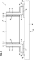
- FIG. 1 shows - schematically - an embodiment of a connection assembly 1.
- the connection assembly 1 comprises an electronic component 2.
- the electronic component 2 has in this embodiment, an electronic component 3, in this embodiment, a capacitor, in particular a ceramic capacitor formed on.
- the electronic component 3 has an electrical connection 4 and an electrical connection 5.
- the electrical connections 4 and 5 are each formed as an electrically conductive layer, which enclose the electronic component 3, in this embodiment, the capacitor, between each other and which extend parallel to each other.
- the component 2 also has a connection element 8, wherein the connection element 8 is formed by an angle element.
- the connection element 8 has a fastening foot 14, which is formed by a leg of the connection element 8, and a further leg 18, wherein the connection leg 18 has a contact surface 20, which faces the connection 5, and by means of a solder 6 to the connection 5 cohesively soldered.
- the leg of the connecting element 8, which forms the fastening foot 14, extends at a right angle to the connecting leg 18.
- connection element 8 has two metal layers, namely a base layer 10 and further metal layer 12, which lie on one another and are connected to one another in a material-locking manner.
- the cohesive connection between the base layer 10 and the further metal layer 12 is produced in this embodiment by means of roll cladding.
- the base layer 10 is formed in this embodiment of an iron-nickel alloy, wherein the nickel content is 42 percent.
- the further metal layer 12 is formed in this embodiment by a copper layer.
- a thickness extension of the further metal layer 12 in this embodiment is one third of the thickness extension of the base layer 10.
- a thickness extension of the base layer 10 is 0.6 millimeters and a thickness extension of the further metal layer 12, in this embodiment of the copper layer, 0.2 millimeters.
- a layer arrangement of the connection element 8 30 percent more heat can be dissipated from the component 2 via the connection element 8 in comparison to a connection element which comprises only the base layer 10.
- the mounting foot 14 is connected in this embodiment by means of a solder 25 with an electrically conductive layer 23, in particular a conductor track, a circuit substrate 22.
- the circuit carrier 22 has an electrically insulating layer 45, in particular a fiber-reinforced epoxy resin layer or a ceramic layer, which is connected to the electrically conductive layer 23 as a component of the circuit carrier 22.
- the circuit carrier 22 also has an electrically conductive layer 24, in particular a conductor track, which is soldered by means of a solder 26 with the Besfest Trentsfuß 15 of a connection element 9, and is electrically conductively connected to the terminal 4 of the device 2.
- the connection element 9 is in this embodiment part of the component 2, wherein the connecting element 9 as the connecting element 8 is formed.
- the connection element 9 has a connection leg 19, which has a contact surface 21, which faces the electrical 4, formed by an electrically conductive layer and is soldered by means of a solder 7 to the electrical connection 4 of the device 2.
- connection leg 19 another leg, formed by a mounting foot 15, formed.
- connection element 9 has a metal layer, which forms a base layer 11.
- the base layer 11 corresponds to the base layer 10 of the connection element 8.
- a further metal layer 13 in this exemplary embodiment a copper layer, which is cohesively bonded by means of roll bonding, is connected to the base layer 11.
- the further metal layer 13 has, in this exemplary embodiment, a thickness extension which amounts to one third of a thickness extent of the base layer 11.
- the component 2 can be placed on the circuit carrier 3, wherein the circuit carrier 3, in particular the electrically conductive layers 23 and 24, each with a solder paste, as Lotstoff 25 or 26 may be printed.
- the component 2 can then be placed on the circuit carrier 22 for soldering to the circuit carrier 22.
- the mounting foot 14 of the connecting element 8 with a contact surface 16 of the mounting foot 14, which forms a stand surface in this embodiment, are placed on the solder 25 and the mounting foot 15 of the connecting element 9, with a contact surface 17, which forms a standing surface of the connecting element 9 to be placed on the solder 26.
- connection arrangement 1 For soldering the component 2 to the circuit carrier 22, the connection arrangement 1 can then be reflow-soldered in a soldering oven.
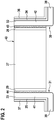
- FIG. 2 shows - schematically - an embodiment of a device 40.
- the device 40 has in this embodiment, an electrical component 27.
- the electrical component 27 is formed for example by a diode, in particular a semiconductor diode, a capacitor or a resistor.
- the electrical component 27 can also be designed as a capacitor, in particular as a ceramic capacitor or as a resistor.
- the electrical component 27 has an electrical connection 28, an electrical connection 29.
- the electrical connection 28 is connected by means of a solder 43 to a connection leg 42 of a connection element 30.
- the connecting element 30 has an integrally formed on the connecting leg 42 mounting foot 38 as another leg. The mounting foot 38 and the connecting leg 42 extend in this embodiment at a right angle to each other.
- connection element 30 comprises a metal layer 32 as the base layer, which is connected in a material-bonded manner to a further metal layer 34, which has a greater thermal conductivity than the base layer 32.
- the further metal layer 34 with the greater electrical conductivity than the base layer 32 is materially connected to a further metal layer 36, wherein the further metal layer 36 is formed from the metal of the base layer 32.
- the base layer 32 and the further metal layer 36 are formed in this embodiment of an iron-nickel alloy, wherein a nickel content of the alloy is 42 percent.
- the further metal layer 34 which has a greater thermal conductivity than the metal layers 32 and 36, is formed in this embodiment by a copper layer.
- a thickness extension In this embodiment, the thickness of the further metal layer 34 is 1/3 of the thickness of the base layer 32. Thickness extension of the further metal layer 36 in this exemplary embodiment is half the thickness of the base layer 32.
- the component 40 also has a further electrical connection 29, which is connected by means of a soldering agent 44 to a connection leg 41 of a connection element 31.
- the connection element 31 has a fastening foot 39, which forms a leg of the connection element 31.
- the mounting foot 39 and the connecting leg 41 of the connecting element 31 each extend at a right angle to each other.
- connection element 31 comprises a metal layer as the base layer 33, which is connected in a material-locking manner, in this embodiment by means of roll cladding, to a further metal layer 35.
- the metal layers 33 and 35 are directly adjacent to each other in this embodiment.
- the further metal layer 35 has in this embodiment, a greater thermal conductivity than the base layer 33.
- the further metal layer 35 is in this embodiment, with a further metal layer 37 cohesively connected.
- the metal layers 33 and 37 enclose the further metal layer 35 - in the manner of a sandwich - between each other.
- connection element 30 the metal layers 32 and 36 between the other metal layer 34 - in the manner of a sandwich - between each other.
- the further metal layer 35 is formed in this embodiment as a copper layer.
- the base layer 33 and the further metal layer 37 are formed in this embodiment by an iron alloy comprising 42 percent nickel.
- connection element 30 can instead of the connection element 8 in Fig. 1 with the electronic component 3, and there with the electrical connection 5, be soldered.
- connection element 31 can instead of the connection element 9 in FIG. 1 with the electronic component 3, and there with the electrical Terminal 4, be soldered.
- the electronic component 3 can thus have the connection elements 30 and 31 instead of the connection elements 8 and 9.
- the respectively one mounting leg forming legs of the connecting elements 30 and 31 are in this embodiment from each other.
- the legs formed by the attachment feet 38 and 39 may be assigned to each other.
- the mounting feet 38 and 39 each extend parallel to the electronic component 27, so that in the case of a connection arrangement such as the connector assembly 1, the mounting feet 38 and 39 are disposed between the electronic component 27 and the circuit carrier 22.
Landscapes
- Engineering & Computer Science (AREA)
- Power Engineering (AREA)
- Microelectronics & Electronic Packaging (AREA)
- Manufacturing & Machinery (AREA)
- Chemical & Material Sciences (AREA)
- Ceramic Engineering (AREA)
- Inorganic Chemistry (AREA)
- Structures For Mounting Electric Components On Printed Circuit Boards (AREA)
- Cooling Or The Like Of Electrical Apparatus (AREA)
- Multi-Conductor Connections (AREA)
- Details Of Resistors (AREA)
Description
- Die Erfindung betrifft ein elektronisches Bauelement. Das elektronische Bauelement weist ein elektrisches Bauteil mit zwei elektrischen Anschlüssen auf, welche jeweils an zueinander gegenüberliegenden Flächen, insbesondere Stirnflächen des Bauteils ausgebildet sind. Das Bauelement weist für jeden Anschluss wenigstens ein elektrisch leitfähiges Anschlusselement auf. Das Anschlusselement weist einen Befestigungsfuß zum Verbinden mit einem Schaltungsträger auf, wobei das Anschlusselement mit dem elektrischen Anschluss des Bauelements stoffschlüssig verbunden und ausgebildet ist, das Bauelement zu tragen.
- Elektronische Bauelemente mit elektrischen Anschlüssen aus dem Stand der Technik sind beispielsweise aus der
EP 2 131 374 A1 , derJP H01 289151 A US 4 158 218 A , derDE 27 31 998 A1 , derUS 2011/075386 A1 und derUS 2002/009610 A1 bekannt. - Erfindungsgemäß weist das Anschlusselement wenigstens auf einem Abschnitt des Anschlusselements wenigstens zwei Metallschichten auf, wobei die Metallschichten jeweils aus zueinander verschiedenen Metallen gebildet sind. Die Metallschichten sind miteinander stoffschlüssig verbunden, wobei eine Basisschicht der Metallschichten mit dem Anschluss verbunden ist, und im Bereich des Befestigungsfußes zum elektrischen Verbinden, insbesondere stoffschlüssigen Verbinden, insbesondere Lötverbinden, Sinterverbinden, oder elektrisch leitfähigen Klebverbinden mit einem Schaltungsträger ausgebildet ist. Bevorzugt ist die wenigstens eine weitere Metallschicht der Metallschichten zu der Basisschicht thermisch oder zusätzlich elektrisch parallel geschaltet. Bevorzugt weist eine weitere Metallschicht, insbesondere die mit der Basisschicht stoffschlüssig verbundene Metallschicht, eine größere thermische Leitfähigkeit auf als die Basisschicht. So kann vorteilhaft von dem elektronischen Bauelement erzeugte Verlustwärme über das Anschlusselement mit verbesserter Wärmeleitfähigkeit abgeführt werden, im Vergleich zu einem Anschlusselement, welches nur aus der Basisschicht gebildet ist. Weiter vorteilhaft kann so über dasselbe Bauelement eine größere Verlustleistung erzeugt werden, verglichen mit einem Bauelement, welches ein Anschlusselement, bestehend aus der Basisschicht, aufweist.
- Bevorzugt sind die Metallschichten mindestens von der Verbindung zum Anschluss des Bauelements, bis hin zum Befestigungsfuß, insbesondere ununterbrochen, stoffschlüssig miteinander verbunden. Die stoffschlüssige Verbindung kann beispielsweise durch Plattieren, insbesondere Walzplattieren, Elektroplattieren, oder kathodisches Aufstäuben, oder durch Hartlöten oder durch Laserschweißen erzeugt werden. So kann das Anschlusselement, und so auch das Bauelement, vorteilhaft aufwandsgünstig bereitgestellt werden. So kann beispielsweise zum Erzeugen des Anschlusselements, insbesondere eines Anschlusswinkelelements, ein Blech umfassend die zwei Metallschichten, nämlich die zuvor genannte Basisschicht und die weitere Metallschicht, welche eine größere Wärmeleitfähigkeit aufweist als die Basisschicht, dadurch erzeugt werden, dass die Metallschichten mittels Plattieren, insbesondere Walzplattieren miteinander verbunden werden. Das so doppelschichtig ausgebildete Blech kann dann mittels eines Stanz- und/oder Umformprozesses zu dem abgewinkelten Anschlusselement geformt werden.
- Vorteilhaft braucht so zum Erzeugen des Bauelements mit einem Anschlusselement, welches das elektronische Bauteil aufweist, ein Herstellungsprozess nicht grundsätzlich verändert werden.
Vorteilhaft kann nämlich ein Anschlusselement, das nur aus einer Metallschicht gebildet ist, durch ein Anschlusselement umfassend wenigstens zwei Metallschichten ersetzt werden. Dadurch kann ein thermisch verbessertes Bauelement gebildet sein.
Bevorzugt weist das Anschlusselement dazu wenigstens zwei, nur zwei, oder drei Metallschichten auf. - In einer bevorzugten Ausführungsform ist die Basisschicht durch eine Legierung, umfassend Eisen, gebildet, und die weitere Schicht mit der größeren thermischen Leitfähigkeit als die Basisschicht, durch eine Kupferschicht gebildet.
- Dadurch kann das Bauelement vorteilhaft aufwandsgünstig bereitgestellt werden. Vorteilhaft braucht im Falle von Kupfer als weitere Schicht eine Schichtdicke der weiteren Metallschicht nur einen Teil der Schichtdicke der Basisschicht betragen, um so eine deutliche Verbesserung der Wärmeleitfähigkeit des Anschlusselements zu erzeugen.
- Bevorzugt beträgt eine Schichtdicke der mit der Basisschicht unmittelbar verbundenen weiteren Metallschicht zwischen einem Zehntel und der Hälfte der Schichtdicke der Basisschicht. Beispielsweise beträgt eine Schichtdicke der weiteren Schicht, als Kupferschicht, ein Drittel der Schichtdicke der Basisschicht, insbesondere einer Eisenlegierungs-Schicht. Die Basisschicht ist beispielsweise durch eine Legierung, umfassend 30 bis 45 Prozent Nickel oder zusätzlich wenigstens einen weiteren Legierungsbestandteil, und als übrigen Bestandteil oder Hauptbestandteil Eisen gebildet. Vorteilhaft weist die Basisschicht aus einer solchen Legierung eine hinreichend gute elektrische Leitfähigkeit und einen geringen thermische Ausdehnungskoeffizienten auf. Der thermische Ausdehnungskoeffizient einer solchen Basisschicht beträgt bevorzugt weniger als 10 ppm pro Kelvin.
- In einer bevorzugten Ausführungsform ist das Bauelement ein Kondensator, insbesondere ein keramischer Kondensator oder ein Folienkondensator, beispielsweise ein SMD-Folienkondensator (SMD = Surface-Mounted-Device). So kann vorteilhaft ein Leistungskondensator als Bauelement gebildet sein, welcher im Vergleich zu demselben Leistungskondensator mit einem Anschlusselement, gebildet aus nur einer Basisschicht, eine größere Wärmeleistung erzeugen und auch abführen kann.
- Bevorzugt weist das elektronische Bauelement ein elektrisches Bauteil, insbesondere einen Kondensator, eine Diode oder einen Widerstand mit einer Quaderform oder Zylinderform auf, wobei Stirnflächen des Bauteils jeweils durch einen elektrischen Anschluss gebildet sind. Dadurch kann das Bauelement vorteilhaft platzsparend mit dem Anschlusselement mit einem Schaltungsträger verlötet werden.
- In einer bevorzugten Ausführungsform ist das Bauteil ein Widerstand oder eine Diode, insbesondere eine Halbleiterdiode, bevorzugt Leistungs-Halbleiterdiode. Der Widerstand und/oder die Diode sind jeweils ausgebildet, mit einem Schaltungsträger verlötet, insbesondere reflow-verlötet, selektivverlötet, oder wellenverlötet zu werden. Dazu kann das Bauelement mit dem Befestigungsfuß auf den Schaltungsträger und auch auf eine elektrisch leitfähige Schicht, insbesondere eine Leiterbahn des Schaltungsträgers, gestellt werden, wobei die elektrisch leitfähige Schicht mit einer Lotpaste bedruckt worden ist. In einem anschließenden Schritt zum Verlöten des Bauelements mit dem Schaltungsträger kann der Schaltungsträger zusammen mit dem Bauelement - beispielsweise in einem Reflow-Lötofen - verlötet werden.
- Bevorzugt ist das Bauelement zum Lötverbinden, bevorzugt Reflow-Lötverbinden mit dem Schaltungsträger ausgebildet. Durch die gute thermische Anbindung an den Schaltungsträger ist das Bauelement gut gekühlt. Vorteilhaft braucht das Bauelement, insbesondere der zuvor erwähnte Kondensator, Widerstand oder die Diode, nicht zusätzlich durch einen weiteren Kühlkörper gekühlt werden, und so auch nicht an einen weiteren, gesonderten Kühlkörper, beispielsweise eine Konvektionsrippen aufweisenden Aluminiumkühlkörper, angekoppelt werden, um über das Bauelement größere Leistungen führen zu können und so auch größere Verlustleistungen in Form von Verlustwärme zu erzeugen.
- Die weitere Metallschicht, welche mit der Basisschicht stoffschlüssig verbunden ist, ist bevorzugt eine Kupferschicht, eine Aluminiumschicht oder eine Silberschicht. Die Silberschicht weist vorteilhaft eine große Wärmeleitfähigkeit auf, sodass die weitere Metallschicht als Silberschicht, verglichen mit einer Aluminium- oder Kupferschicht, dünner ausgebildet sein kann, um dieselbe Wärmeleistung über das Anschlusselement zum Schaltungsträger hin zu führen.
- In einer bevorzugten Ausführungsform des Bauelements ist das Anschlusselement ein Winkelelement, welches zwei aneinander angeformte und sich in einem vorbestimmten Winkel zueinander erstreckende Schenkel aufweist. Ein Schenkel des Anschlusselements bildet dabei einen Befestigungsfuß, wobei der weitere Schenkel einen Anschlussschenkel bildet, welcher mit dem elektrischen Anschluss verbunden, insbesondere lötverbunden mittels eines leitfähigen Klebstoffs elektrisch leitfähig klebeverbunden, oder schweißverbunden ist. Die Schweißverbindung ist beispielsweise mittels Widerstandsschweißen oder Laserschweißen erzeugt. So kann das Bauelement vorteilhaft aufwandsgünstig mit einem Befestigungsfuß versehen sein. Erfindungsgemäß weist das Anschlusselement eine weitere Metallschicht auf, welche aus dem Metall der Basisschicht gebildet ist. Die Metallschicht mit der größeren thermischen Leitfähigkeit im Vergleich zu der Basisschicht ist zwischen der Basisschicht und der weiteren Metallschicht aus dem Metall der Basisschicht - insbesondere nach Art eines Sandwiches - eingeschlossen. Bevorzugt ist die weitere Metallschicht aus dem Metall der Basisschicht mit der weiteren Metallschicht mit der größeren thermischen Leitfähigkeit stoffschlüssig verbunden. Auf diese Weise ist ein stoffschlüssig verbundener Sandwichverbund gebildet, welcher vorteilhaft - beispielsweise mittels Walzplattieren - als Rohblech-Ausgangsmaterial zum Erzeugen des Anschlusselements aufwandsgünstig bereitgestellt werden kann. Das so gebildete Anschlusselement weist vorteilhaft bei Temperaturveränderungen eine kleinere Verkrümmung quer zu seiner flachen Erstreckung auf, insoweit ein Bimetalleffekt, erzeugt durch zueinander verschiedene Wärmeausdehnungskoeffizienten der zueinander verschiedenen Metallschichten, durch die weitere Metallschicht, welche aus dem Metall der Basisschicht gebildet ist, kompensiert werden kann.
- Im Folgenden wird die Erfindung anhand von Figuren und weiteren Ausführungsbeispielen beschrieben. Weitere vorteilhafte Ausführungsvarianten ergeben sich aus den in den abhängigen Ansprüchen und in den Figuren beschriebenen Merkmalen.
-
Figur 1 zeigt ein Ausführungsbeispiel für eine Verbindungsanordnung mit einem quaderförmigen elektronischen Bauelement, welches an zueinander gegenüberliegenden Stirnseiten angeordnete elektrische Anschlüsse aufweist, welche mittels eines doppelschichtig ausgebildeten Anschlusselements mit einem Schaltungsträger lötverbunden sind; -
Figur 2 zeigt ein Ausführungsbeispiel für ein elektronisches Bauelement, welches Anschlusselemente mit jeweils drei Metallschichten aufweist. -
Figur 1 zeigt - schematisch - ein Ausführungsbeispiel für eine Verbindungsanordnung 1. Die Verbindungsanordnung 1 weist ein elektronisches Bauelement 2 auf. Das elektronische Bauelement 2 weist in diesem Ausführungsbeispiel ein elektronisches Bauteil 3, in diesem Ausführungsbeispiel einen Kondensator, insbesondere einen keramisch ausgebildeten Kondensator, auf. Das elektronische Bauteil 3 weist einen elektrischen Anschluss 4 und einen elektrischen Anschluss 5 auf. Die elektrischen Anschlüsse 4 und 5 sind jeweils als elektrisch leitfähige Schicht ausgebildet, welche das elektronische Bauteil 3, in diesem Ausführungsbeispiel den Kondensator, zwischen einander einschließen und welche sich parallel zueinander erstrecken. - Das Bauelement 2 weist auch ein Anschlusselement 8 auf, wobei das Anschlusselement 8 durch ein Winkelelement gebildet ist. Das Anschlusselement 8 weist einen Befestigungsfuß 14 auf, welcher durch einen Schenkel des Anschlusselements 8 gebildet ist, und einen weiteren Schenkel 18, wobei der Anschlussschenkel 18 eine Kontaktfläche 20 aufweist, welche zu dem Anschluss 5 weist, und mittels eines Lotmittels 6 mit dem Anschluss 5 stoffschlüssig lötverbunden ist.
- Der Schenkel des Anschlusselements 8, welcher den Befestigungsfuß 14 bildet, erstreckt sich in einen rechten Winkel zu dem Anschlussschenkel 18.
- Das Anschlusselement 8 weist in diesem Ausführungsbeispiel zwei Metallschichten auf, nämlich eine Basisschicht 10 und weitere Metallschicht 12, welche jeweils aufeinander liegen und stoffschlüssig miteinander verbunden sind. Die stoffschlüssige Verbindung zwischen der Basisschicht 10 und der weiteren Metallschicht 12 ist in diesem Ausführungsbeispiel mittels Walzplattieren erzeugt.
- Die Basisschicht 10 ist in diesem Ausführungsbeispiel aus einer Eisen-Nickel-Legierung gebildet, wobei der Nickelanteil 42 Prozent beträgt. Die weitere Metallschicht 12 ist in diesem Ausführungsbeispiel durch eine Kupferschicht gebildet. Eine Dickenerstreckung der weiteren Metallschicht 12 beträgt in diesem Ausführungsbeispiel einem Drittel der Dickenerstreckung der Basisschicht 10.
- Beispielsweise beträgt eine Dickenerstreckung der Basisschicht 10 0,6 Millimeter und eine Dickenerstreckung der weiteren Metallschicht 12, in diesem Ausführungsbeispiel der Kupferschicht, 0,2 Millimeter. Bei einer solchen Schichtanordnung des Anschlusselements 8 kann im Vergleich zu einem Anschlusselement, welches nur die Basisschicht 10 umfasst, 30 Prozent mehr Wärme von dem Bauelement 2 über das Anschlusselement 8 abgeführt werden.
- Der Befestigungsfuß 14 ist in diesem Ausführungsbeispiel mittels eines Lotmittels 25 mit einer elektrisch leitfähigen Schicht 23, insbesondere einer Leiterbahn, eines Schaltungsträgers 22, verbunden. Der Schaltungsträger 22 weist in diesem Ausführungsbeispiel eine elektrisch isolierende Schicht 45, insbesondere eine faserverstärkte Epoxidharzschicht oder eine Keramikschicht auf, welche mit der elektrisch leitfähigen Schicht 23 als Bestandteil des Schaltungsträgers 22 verbunden ist. Der Schaltungsträger 22 weist auch eine elektrisch leitfähige Schicht 24, insbesondere eine Leiterbahn auf, welche mittels eines Lotmittels 26 mit dem Besfestigungsfuß 15 eines Anschlusselements 9 verlötet ist, und so mit dem Anschluss 4 des Bauelements 2 elektrisch leitfähig verbunden ist. Das Anschlusselement 9 ist in diesem Ausführungsbeispiel Bestandteil des Bauelements 2, wobei das Anschlusselement 9 wie das Anschlusselement 8 ausgebildet ist. Dazu weist das Anschlusselement 9 einen Anschlussschenkel 19 auf, welcher eine Kontaktfläche 21 aufweist, welche dem elektrischen 4, gebildet durch eine elektrisch leitfähige Schicht zugewandt ist und mittels eines Lotmittels 7 mit dem elektrischen Anschluss 4 des Bauelements 2 verlötet ist.
- An dem Anschlussschenkel 19 ist ein weiterer Schenkel, gebildet durch einen Befestigungsfuß 15, angeformt. Der Schenkel, gebildet durch den Befestigungsfuß 15, und der Anschlussschenkel 19, erstrecken sich jeweils in einem rechten Winkel zueinander.
- Das Anschlusselement 9 weist eine Metallschicht auf, welche eine Basisschicht 11 bildet. Die Basisschicht 11 entspricht der Basisschicht 10 des Anschlusselements 8. Mit der Basisschicht 11 ist in diesem Ausführungsbeispiel eine mittels Walzplattieren stoffschlüssig verbundene weitere Metallschicht 13, in diesem Ausführungsbeispiel eine Kupferschicht, verbunden. Die weitere Metallschicht 13 weist in diesem Ausführungsbeispiel eine Dickenerstreckung auf, welche ein Drittel einer Dickenerstreckung der Basisschicht 11 beträgt.
- Zum Erzeugen der Verbindungsanordnung 1 kann das Bauelement 2 auf den Schaltungsträger 3 gestellt werden, wobei der Schaltungsträger 3, insbesondere die elektrisch leitfähigen Schichten 23 und 24, jeweils mit einer Lotpaste, als Lotmittel 25 beziehungsweise 26 bedruckt sein kann.
- Das Bauelement 2 kann dann zum Lötverbinden mit dem Schaltungsträger 22 auf den Schaltungsträger 22 gestellt werden. Dazu kann der Befestigungsfuß 14 des Anschlusselements 8 mit einer Kontaktfläche 16 des Befestigungsfußes 14, welcher in diesem Ausführungsbeispiel eine Standfläche bildet, auf das Lotmittel 25 gesetzt werden und der Befestigungsfuß 15 des Anschlusselements 9, mit einer Kontaktfläche 17, welche eine Standfläche des Anschlusselements 9 bildet, auf das Lotmittel 26 gesetzt werden.
- Zum Verlöten des Bauelements 2 mit dem Schaltungsträger 22 kann dann die Verbindungsanordnung 1 in einem Lötofen Reflow-verlötet werden.
-
Figur 2 zeigt - schematisch - ein Ausführungsbeispiel für ein Bauelement 40. Das Bauelement 40 weist in diesem Ausführungsbeispiel ein elektrisches Bauteil 27 auf. Das elektrische Bauteil 27 ist beispielsweise durch eine Diode, insbesondere eine Halbleiterdiode, einen Kondensator oder einen Widerstand gebildet. - Das elektrische Bauteil 27 kann in einer anderen Ausführungsform auch als Kondensator, insbesondere als keramischer Kondensator oder als Widerstand, ausgebildet sein. Das elektrische Bauteil 27 weist einen elektrischen Anschluss 28, einen elektrischen Anschluss 29 auf. Der elektrische Anschluss 28 ist mittels eines Lotmittels 43 mit einem Anschlussschenkel 42 eines Anschlusselements 30 verbunden. Das Anschlusselement 30 weist einen an den Anschlussschenkel 42 angeformten Befestigungsfuß 38 als weiteren Schenkel auf. Der Befestigungsfuß 38 und der Anschlussschenkel 42 erstrecken sich in diesem Ausführungsbeispiel in einem rechten Winkel zueinander.
- Das Anschlusselement 30 umfasst in diesem Ausführungsbeispiel eine Metallschicht 32 als Basisschicht, welche mit einer weiteren Metallschicht 34, welche eine größere thermische Leitfähigkeit aufweist als die Basisschicht 32, stoffschlüssig verbunden. Die weitere Metallschicht 34 mit der größeren elektrischen Leitfähigkeit als die Basisschicht 32 ist mit einer weiteren Metallschicht 36 stoffschlüssig verbunden, wobei die weitere Metallschicht 36 aus dem Metall der Basisschicht 32 gebildet ist. Auch so kann vorteilhaft ein Bimetalleffekt, welcher aufgrund zueinander verschiedener Wärmeausdehnungskoeffizienten der Basisschicht 32 und der weiteren Metallschicht 34 entstehen kann, kompensiert werden.
- Die Basisschicht 32 und die weitere Metallschicht 36 sind in diesem Ausführungsbeispiel aus einer Eisen-Nickel-Legierung gebildet, wobei ein Nickelanteil der Legierung 42 Prozent beträgt. Die weitere Metallschicht 34, welche eine größere thermische Leitfähigkeit aufweist als die Metallschichten 32 und 36, ist in diesem Ausführungsbeispiel durch eine Kupferschicht gebildet. Eine Dickenerstreckung der weiteren Metallschicht 34 beträgt in diesem Ausführungsbeispiel 1/3 der Dickenerstreckung der Basisschicht 32. Eine Dickenerstreckung der weiteren Metallschicht 36 beträgt in diesem Ausführungsbeispiel die Hälfte der Dickenerstreckung der Basisschicht 32.
- Das Bauelement 40 weist in diesem Ausführungsbeispiel auch einen weiteren elektrischen Anschluss 29 auf, welcher mittels eines Lotmittels 44 mit einem Anschlussschenkel 41 eines Anschlusselements 31 verbunden ist. Das Anschlusselement 31 weist einen Befestigungsfuß 39 auf, welcher einen Schenkel des Anschlusselements 31 bildet. Der Befestigungsfuß 39 und der Anschlussschenkel 41 des Anschlusselements 31 erstrecken sich jeweils in einem rechten Winkel zueinander.
- Das Anschlusselement 31 umfasst in diesem Ausführungsbeispiel eine Metallschicht als Basisschicht 33, welche stoffschlüssig, in diesem Ausführungsbeispiel mittels Walzplattieren, mit einer weiteren Metallschicht 35 verbunden ist. Die Metallschichten 33 und 35 liegen in diesem Ausführungsbeispiel unmittelbar aufeinander. Die weitere Metallschicht 35 weist in diesem Ausführungsbeispiel eine größere thermische Leitfähigkeit als die Basisschicht 33. Die weitere Metallschicht 35 ist in diesem Ausführungsbeispiel mit einer weiteren Metallschicht 37 stoffschlüssig verbunden. Die Metallschichten 33 und 37 schließen die weitere Metallschicht 35 - nach Art eines Sandwiches - zwischen einander ein.
- Bei dem Anschlusselement 30 schließen die Metallschichten 32 und 36 die weitere Metallschicht 34 - nach Art eines Sandwiches - zwischen einander ein. Die weitere Metallschicht 35 ist in diesem Ausführungsbeispiel als Kupferschicht ausgebildet. Die Basisschicht 33 und die weitere Metallschicht 37 sind in diesem Ausführungsbeispiel durch eine Eisenlegierung, umfassend 42 Prozent Nickel, gebildet.
- Das Anschlusselement 30 kann anstelle des Anschlusselements 8 in
Fig. 1 mit dem elektronischen Bauteil 3, und dort mit dem elektrischen Anschluss 5, lötverbunden sein. Das Anschlusselement 31 kann anstelle des Anschlusselements 9 inFigur 1 mit dem elektronischen Bauteil 3, und dort mit dem elektrischen Anschluss 4, lötverbunden sein. Das elektronische Bauteil 3 kann somit anstelle der Anschlusselemente 8 und 9 die Anschlusselemente 30 beziehungsweise 31 aufweisen. - Die jeweils einen Befestigungsfuß bildenden Schenkel der Anschlusselemente 30 und 31 weisen in diesem Ausführungsbeispiel voneinander ab. In einer anderen Ausführungsform können die durch die Befestigungsfüße 38 und 39 gebildeten Schenkel aufeinander zuweisen. In dieser Ausführungsform erstrecken sich die Befestigungsfüße 38 und 39 jeweils parallel zu dem elektronischen Bauteil 27, sodass im Fall einer Verbindungsanordnung, wie die Verbindungsanordnung 1, die Befestigungsfüße 38 und 39 zwischen dem elektronischen Bauteil 27 und dem Schaltungsträger 22 angeordnet sind.
Claims (9)
- Elektronisches Bauelement (2, 40), umfassend ein elektrisches Bauteil (3, 27) mit zwei elektrischen Anschlüssen (4, 5, 28, 29), welche jeweils an zueinander gegenüberliegenden Flächen des Bauteils (3, 27) ausgebildet sind, wobei das Bauelement (2, 40) für jeden der Anschlüsse (4, 5, 28, 29) ein elektrisch leitfähiges Anschlusselement (8, 9, 30, 31) aufweist, wobei das Anschlusselement einen Befestigungsfuß (14, 15, 38, 39) zum stoffschlüssigen elektrischen Verbinden, insbesondere Lötverbinden mit einem Schaltungsträger (22) aufweist, wobei das Anschlusselement (8, 9, 30, 31) mit dem elektrischen Anschluss (4, 5, 28, 29) stoffschlüssig verbunden und ausgebildet ist, das Bauelement (2, 40) zu tragen, wobei das Anschlusselement (8, 9, 30, 31) wenigstens zwei miteinander stoffschlüssig verbundene Metallschichten (10, 12, 11, 13, 32, 33, 34, 35, 36, 37), jeweils gebildet aus zueinander verschiedenen Metallen aufweist, wobei eine Basisschicht (10, 11, 32, 33) der Metallschichten mit dem elektrischen Anschluss (4, 5, 28, 29) verbunden ist und im Bereich des Befestigungsfußes (14, 15, 38, 39) zum Lötverbinden mit einem Schaltungsträger (22) ausgebildet ist, so dass die wenigstens eine weitere Metallschicht (12, 13, 34, 35) der Metallschichten zu der Basisschicht (10, 11, 32, 33) thermisch parallel geschaltet ist, wobei die weitere Metallschicht (12, 13, 34, 35) eine größere thermische Leitfähigkeit aufweist als die Basisschicht (10, 11, 32, 33)
dadurch gekennzeichnet, dass
das Anschlusselement (8, 9, 30, 31) eine weitere Metallschicht (36, 37) aufweist, welche aus dem Metall der Basisschicht (10, 11, 32, 33) gebildet ist, wobei die Metallschicht mit der größeren thermischen Leitfähigkeit zwischen der Basisschicht (10, 11, 32, 33) und der weiteren Metallschicht (36, 37) aus dem Metall der Basisschicht (10, 11, 32, 33) - insbesondere nach Art eines Sandwiches - eingeschlossen ist. - Bauelement (2, 40) nach Anspruch 1,
dadurch gekennzeichnet, dass
die Metallschichten (10, 11, 12, 13, 32, 33, 34, 35, 36, 37) mindestens von der Verbindung zum Anschluss (4, 5, 28, 29) des Bauelements (2, 40) bis hin zum Befestigungsfuß (14, 15, 38, 39) stoffschlüssig miteinander verbunden sind. - Bauelement (2, 40) nach einem der vorhergehenden Ansprüche,
dadurch gekennzeichnet, dass
die Basisschicht (10, 11, 32, 33) durch eine Legierung umfassend Eisen gebildet ist und die weitere Metallschicht (12, 13, 34, 35) mit der größeren thermischen Leitfähigkeit als die Basisschicht (12, 13, 34, 35) durch eine Kupferschicht oder Aluminiumschicht gebildet ist. - Bauelement (2, 40) nach Anspruch 1 oder 2,
dadurch gekennzeichnet, dass
die Basisschicht (10, 11, 32, 33) zwischen 30 und 45 Prozent Nickel und als weiteren Bestandteil Eisen und aufweist. - Bauelement (2, 40) nach einem der vorhergehenden Ansprüche,
dadurch gekennzeichnet, dass
eine Schichtdicke der mit der Basisschicht (10, 11, 32, 33) verbundenen weiteren Metallschicht (12, 13, 34, 35) zwischen einem Zehntel und der Hälfte der Schichtdicke der Basisschicht (10, 11, 32, 33) beträgt. - Bauelement (2, 40) nach einem der vorhergehenden Ansprüche,
dadurch gekennzeichnet, dass
das Anschlusselement (8, 9, 30, 31) ein Winkelelement ist, welches zwei aneinander angeformte und sich in einem vorbestimmten Winkel zueinander erstreckende Schenkel (14, 18, 15, 19, 38, 39, 41, 42) aufweist, wobei ein Schenkel den Befestigungsfuß (14, 15, 38, 39) bildet, und der weitere Schenkel (18, 19, 41, 42) einen Anschlussschenkel bildet, welcher mit dem elektrischen Anschluss (4, 5, 28, 29) verbunden ist. - Bauelement (2, 40) nach einem der vorhergehenden Ansprüche,
dadurch gekennzeichnet, dass
die stoffschlüssig miteinander verbundenen Metallschichten (10, 12, 11, 13, 32, 33, 34, 35, 36, 37) mittels Walzplattieren miteinander verbunden sind. - Bauelement (2, 40) nach einem der vorhergehenden Ansprüche,
dadurch gekennzeichnet, dass
das Bauteil (3, 27) ein Kondensator, insbesondere keramischer Kondensator ist. - Bauelement (2, 40) nach einem der vorhergehenden Ansprüche,
dadurch gekennzeichnet, dass
das Bauteil (3, 27) eine Halbleiterdiode oder ein Widerstand ist.
Applications Claiming Priority (2)
| Application Number | Priority Date | Filing Date | Title |
|---|---|---|---|
| DE102014220802.5A DE102014220802A1 (de) | 2014-10-14 | 2014-10-14 | Elektronisches Bauelement mit einem Anschlusselement |
| PCT/EP2015/069613 WO2016058741A1 (de) | 2014-10-14 | 2015-08-27 | Elektronisches bauelement mit einem anschlusselement |
Publications (2)
| Publication Number | Publication Date |
|---|---|
| EP3207774A1 EP3207774A1 (de) | 2017-08-23 |
| EP3207774B1 true EP3207774B1 (de) | 2018-07-04 |
Family
ID=54014812
Family Applications (1)
| Application Number | Title | Priority Date | Filing Date |
|---|---|---|---|
| EP15756896.5A Not-in-force EP3207774B1 (de) | 2014-10-14 | 2015-08-27 | Elektronisches bauelement mit einem anschlusselement |
Country Status (5)
| Country | Link |
|---|---|
| US (1) | US10249435B2 (de) |
| EP (1) | EP3207774B1 (de) |
| CN (1) | CN106797701B (de) |
| DE (1) | DE102014220802A1 (de) |
| WO (1) | WO2016058741A1 (de) |
Families Citing this family (5)
| Publication number | Priority date | Publication date | Assignee | Title |
|---|---|---|---|---|
| JP2018206813A (ja) * | 2017-05-30 | 2018-12-27 | 株式会社村田製作所 | 積層セラミック電子部品 |
| JP2019009359A (ja) * | 2017-06-27 | 2019-01-17 | 株式会社村田製作所 | 積層セラミック電子部品及びその実装構造 |
| EP3522188A1 (de) * | 2018-02-06 | 2019-08-07 | Siemens Aktiengesellschaft | Kondensatoraufbau und leistungsmodul mit einem leistungselektronischen bauelement |
| DE102018201842A1 (de) | 2018-02-06 | 2019-08-08 | Siemens Aktiengesellschaft | Leistungselektronische Schaltung mit mehreren Leistungsmodulen |
| DE102020205625A1 (de) | 2020-05-05 | 2021-11-11 | Volkswagen Aktiengesellschaft | Verfahren zum Fixieren eines Bauteils auf einem Träger |
Family Cites Families (10)
| Publication number | Priority date | Publication date | Assignee | Title |
|---|---|---|---|---|
| DE2731998A1 (de) * | 1977-07-15 | 1979-01-25 | Draloric Electronic | Elektrischer widerstand |
| US4158218A (en) * | 1977-09-19 | 1979-06-12 | Union Carbide Corporation | Ceramic capacitor device |
| JPH01289151A (ja) * | 1988-05-16 | 1989-11-21 | Toshiba Corp | 集積回路装置 |
| JP3622462B2 (ja) * | 1997-12-16 | 2005-02-23 | 株式会社日立製作所 | 半導体装置 |
| US20020009610A1 (en) | 1997-12-16 | 2002-01-24 | Hanae Shimokawa | Technical field |
| CN101180690B (zh) * | 2005-05-23 | 2011-06-15 | 株式会社村田制作所 | 陶瓷电子元件及其制造方法 |
| US7808770B2 (en) * | 2007-06-27 | 2010-10-05 | Murata Manufacturing Co., Ltd. | Monolithic ceramic capacitor |
| JP5176775B2 (ja) | 2008-06-02 | 2013-04-03 | 株式会社村田製作所 | セラミック電子部品及びその製造方法 |
| US8738863B2 (en) | 2009-09-25 | 2014-05-27 | Intel Corporation | Configurable multi-level buffering in media and pipelined processing components |
| JP5350962B2 (ja) * | 2009-09-30 | 2013-11-27 | 富士通株式会社 | 電子部品、基板ユニット及び情報処理装置 |
-
2014
- 2014-10-14 DE DE102014220802.5A patent/DE102014220802A1/de not_active Withdrawn
-
2015
- 2015-08-27 EP EP15756896.5A patent/EP3207774B1/de not_active Not-in-force
- 2015-08-27 CN CN201580055656.6A patent/CN106797701B/zh not_active Expired - Fee Related
- 2015-08-27 WO PCT/EP2015/069613 patent/WO2016058741A1/de not_active Ceased
- 2015-08-27 US US15/518,746 patent/US10249435B2/en not_active Expired - Fee Related
Non-Patent Citations (1)
| Title |
|---|
| None * |
Also Published As
| Publication number | Publication date |
|---|---|
| CN106797701A (zh) | 2017-05-31 |
| US20170236643A1 (en) | 2017-08-17 |
| US10249435B2 (en) | 2019-04-02 |
| DE102014220802A1 (de) | 2016-04-14 |
| CN106797701B (zh) | 2019-04-12 |
| EP3207774A1 (de) | 2017-08-23 |
| WO2016058741A1 (de) | 2016-04-21 |
Similar Documents
| Publication | Publication Date | Title |
|---|---|---|
| EP1713124B1 (de) | Leistungshalbleitermodul mit Verbindungsbahnen und mit Anschlusselementen, die mit den Verbindungsbahnen verbunden sind | |
| EP3207774B1 (de) | Elektronisches bauelement mit einem anschlusselement | |
| DE102010038246B4 (de) | Oberflächenmontierbares drahtloses Package mit offenem Hohlraum für Hochleistungs-HF-Anwendungen, Verfahren zum Herstellen eines HF Halbleiterpackage und einer HF Halbleiterpackagebaugruppe | |
| EP0920055B1 (de) | Kühlvorrichtung für ein auf einer Leiterplatte angeordnetes, wärmeerzeugendes Bauelement | |
| US20190304702A1 (en) | Electrical connection contact for a ceramic component, a ceramic component, and a component arrangement | |
| DE10306643B4 (de) | Anordnung in Druckkontaktierung mit einem Leistungshalbleitermodul | |
| DE102015122259B4 (de) | Halbleitervorrichtungen mit einer porösen Isolationsschicht | |
| DE102012211952B4 (de) | Leistungshalbleitermodul mit mindestens einem stressreduzierenden Anpasselement | |
| DE102005047566C5 (de) | Anordnung mit einem Leistungshalbleiterbauelement und mit einem Gehäuse sowie Herstellungsverfahren hierzu | |
| DE102004021054B4 (de) | Halbleiterbauelement und Verfahren zu seiner Herstellung | |
| JP2010199171A5 (ja) | チップ部品及び配線基板 | |
| DE112016005794T5 (de) | Schaltungsanordnung und elektrischer Anschlusskasten | |
| DE102016203581A1 (de) | Halbleitervorrichtung und verfahren zum herstellen einer halbleitervorrichtung | |
| WO2016152647A1 (ja) | 回路構成体 | |
| JP5920634B2 (ja) | プリント基板 | |
| JPH11251176A (ja) | セラミック電子部品 | |
| DE102005047567B3 (de) | Leistungshalbleitermodul mit Isolationszwischenlage und Verfahren zu seiner Herstellung | |
| DE102006008807B4 (de) | Anordnung mit einem Leistungshalbleitermodul und einem Kühlbauteil | |
| DE102008019797A1 (de) | Kühlanordnung und Umrichter | |
| JP2016131164A (ja) | 電子制御装置 | |
| WO2019007625A1 (de) | Leistungsmodul mit einem oberseitig und/oder unterseitig elektrisch zu kontaktierenden halbleiterträgerelement und mindestens einem oberflächenmontierten elektrischen kontaktierungselement | |
| DE102014209690A1 (de) | Kommutierungszelle | |
| DE102012103191A1 (de) | Verfahren um Lötbauteile bondbar zu machen | |
| JP3969991B2 (ja) | 面実装電子部品 | |
| DE102008040290A1 (de) | Hybridschaltungsstruktur mit keramischen Schaltungsträgern |
Legal Events
| Date | Code | Title | Description |
|---|---|---|---|
| PUAI | Public reference made under article 153(3) epc to a published international application that has entered the european phase |
Free format text: ORIGINAL CODE: 0009012 |
|
| 17P | Request for examination filed |
Effective date: 20170515 |
|
| AK | Designated contracting states |
Kind code of ref document: A1 Designated state(s): AL AT BE BG CH CY CZ DE DK EE ES FI FR GB GR HR HU IE IS IT LI LT LU LV MC MK MT NL NO PL PT RO RS SE SI SK SM TR |
|
| AX | Request for extension of the european patent |
Extension state: BA ME |
|
| DAV | Request for validation of the european patent (deleted) | ||
| DAX | Request for extension of the european patent (deleted) | ||
| RIC1 | Information provided on ipc code assigned before grant |
Ipc: H01G 4/30 20060101ALN20180219BHEP Ipc: H01G 4/232 20060101ALI20180219BHEP Ipc: H01L 23/495 20060101ALN20180219BHEP Ipc: H05K 1/02 20060101ALI20180219BHEP Ipc: H05K 3/34 20060101AFI20180219BHEP |
|
| GRAP | Despatch of communication of intention to grant a patent |
Free format text: ORIGINAL CODE: EPIDOSNIGR1 |
|
| INTG | Intention to grant announced |
Effective date: 20180409 |
|
| GRAS | Grant fee paid |
Free format text: ORIGINAL CODE: EPIDOSNIGR3 |
|
| GRAA | (expected) grant |
Free format text: ORIGINAL CODE: 0009210 |
|
| AK | Designated contracting states |
Kind code of ref document: B1 Designated state(s): AL AT BE BG CH CY CZ DE DK EE ES FI FR GB GR HR HU IE IS IT LI LT LU LV MC MK MT NL NO PL PT RO RS SE SI SK SM TR |
|
| REG | Reference to a national code |
Ref country code: GB Ref legal event code: FG4D Free format text: NOT ENGLISH |
|
| REG | Reference to a national code |
Ref country code: CH Ref legal event code: EP |
|
| REG | Reference to a national code |
Ref country code: AT Ref legal event code: REF Ref document number: 1015914 Country of ref document: AT Kind code of ref document: T Effective date: 20180715 |
|
| REG | Reference to a national code |
Ref country code: IE Ref legal event code: FG4D Free format text: LANGUAGE OF EP DOCUMENT: GERMAN |
|
| REG | Reference to a national code |
Ref country code: DE Ref legal event code: R096 Ref document number: 502015004963 Country of ref document: DE |
|
| REG | Reference to a national code |
Ref country code: FR Ref legal event code: PLFP Year of fee payment: 4 |
|
| REG | Reference to a national code |
Ref country code: NL Ref legal event code: MP Effective date: 20180704 |
|
| REG | Reference to a national code |
Ref country code: LT Ref legal event code: MG4D |
|
| PG25 | Lapsed in a contracting state [announced via postgrant information from national office to epo] |
Ref country code: NL Free format text: LAPSE BECAUSE OF FAILURE TO SUBMIT A TRANSLATION OF THE DESCRIPTION OR TO PAY THE FEE WITHIN THE PRESCRIBED TIME-LIMIT Effective date: 20180704 |
|
| PG25 | Lapsed in a contracting state [announced via postgrant information from national office to epo] |
Ref country code: FI Free format text: LAPSE BECAUSE OF FAILURE TO SUBMIT A TRANSLATION OF THE DESCRIPTION OR TO PAY THE FEE WITHIN THE PRESCRIBED TIME-LIMIT Effective date: 20180704 Ref country code: IS Free format text: LAPSE BECAUSE OF FAILURE TO SUBMIT A TRANSLATION OF THE DESCRIPTION OR TO PAY THE FEE WITHIN THE PRESCRIBED TIME-LIMIT Effective date: 20181104 Ref country code: RS Free format text: LAPSE BECAUSE OF FAILURE TO SUBMIT A TRANSLATION OF THE DESCRIPTION OR TO PAY THE FEE WITHIN THE PRESCRIBED TIME-LIMIT Effective date: 20180704 Ref country code: NO Free format text: LAPSE BECAUSE OF FAILURE TO SUBMIT A TRANSLATION OF THE DESCRIPTION OR TO PAY THE FEE WITHIN THE PRESCRIBED TIME-LIMIT Effective date: 20181004 Ref country code: GR Free format text: LAPSE BECAUSE OF FAILURE TO SUBMIT A TRANSLATION OF THE DESCRIPTION OR TO PAY THE FEE WITHIN THE PRESCRIBED TIME-LIMIT Effective date: 20181005 Ref country code: BG Free format text: LAPSE BECAUSE OF FAILURE TO SUBMIT A TRANSLATION OF THE DESCRIPTION OR TO PAY THE FEE WITHIN THE PRESCRIBED TIME-LIMIT Effective date: 20181004 Ref country code: SE Free format text: LAPSE BECAUSE OF FAILURE TO SUBMIT A TRANSLATION OF THE DESCRIPTION OR TO PAY THE FEE WITHIN THE PRESCRIBED TIME-LIMIT Effective date: 20180704 Ref country code: PL Free format text: LAPSE BECAUSE OF FAILURE TO SUBMIT A TRANSLATION OF THE DESCRIPTION OR TO PAY THE FEE WITHIN THE PRESCRIBED TIME-LIMIT Effective date: 20180704 Ref country code: CZ Free format text: LAPSE BECAUSE OF FAILURE TO SUBMIT A TRANSLATION OF THE DESCRIPTION OR TO PAY THE FEE WITHIN THE PRESCRIBED TIME-LIMIT Effective date: 20180704 Ref country code: LT Free format text: LAPSE BECAUSE OF FAILURE TO SUBMIT A TRANSLATION OF THE DESCRIPTION OR TO PAY THE FEE WITHIN THE PRESCRIBED TIME-LIMIT Effective date: 20180704 |
|
| PG25 | Lapsed in a contracting state [announced via postgrant information from national office to epo] |
Ref country code: HR Free format text: LAPSE BECAUSE OF FAILURE TO SUBMIT A TRANSLATION OF THE DESCRIPTION OR TO PAY THE FEE WITHIN THE PRESCRIBED TIME-LIMIT Effective date: 20180704 Ref country code: LV Free format text: LAPSE BECAUSE OF FAILURE TO SUBMIT A TRANSLATION OF THE DESCRIPTION OR TO PAY THE FEE WITHIN THE PRESCRIBED TIME-LIMIT Effective date: 20180704 Ref country code: AL Free format text: LAPSE BECAUSE OF FAILURE TO SUBMIT A TRANSLATION OF THE DESCRIPTION OR TO PAY THE FEE WITHIN THE PRESCRIBED TIME-LIMIT Effective date: 20180704 Ref country code: ES Free format text: LAPSE BECAUSE OF FAILURE TO SUBMIT A TRANSLATION OF THE DESCRIPTION OR TO PAY THE FEE WITHIN THE PRESCRIBED TIME-LIMIT Effective date: 20180704 |
|
| REG | Reference to a national code |
Ref country code: CH Ref legal event code: PL |
|
| REG | Reference to a national code |
Ref country code: DE Ref legal event code: R097 Ref document number: 502015004963 Country of ref document: DE |
|
| PG25 | Lapsed in a contracting state [announced via postgrant information from national office to epo] |
Ref country code: MC Free format text: LAPSE BECAUSE OF FAILURE TO SUBMIT A TRANSLATION OF THE DESCRIPTION OR TO PAY THE FEE WITHIN THE PRESCRIBED TIME-LIMIT Effective date: 20180704 Ref country code: CH Free format text: LAPSE BECAUSE OF NON-PAYMENT OF DUE FEES Effective date: 20180831 Ref country code: LU Free format text: LAPSE BECAUSE OF NON-PAYMENT OF DUE FEES Effective date: 20180827 Ref country code: RO Free format text: LAPSE BECAUSE OF FAILURE TO SUBMIT A TRANSLATION OF THE DESCRIPTION OR TO PAY THE FEE WITHIN THE PRESCRIBED TIME-LIMIT Effective date: 20180704 Ref country code: LI Free format text: LAPSE BECAUSE OF NON-PAYMENT OF DUE FEES Effective date: 20180831 Ref country code: EE Free format text: LAPSE BECAUSE OF FAILURE TO SUBMIT A TRANSLATION OF THE DESCRIPTION OR TO PAY THE FEE WITHIN THE PRESCRIBED TIME-LIMIT Effective date: 20180704 |
|
| PLBE | No opposition filed within time limit |
Free format text: ORIGINAL CODE: 0009261 |
|
| REG | Reference to a national code |
Ref country code: BE Ref legal event code: MM Effective date: 20180831 |
|
| STAA | Information on the status of an ep patent application or granted ep patent |
Free format text: STATUS: NO OPPOSITION FILED WITHIN TIME LIMIT |
|
| PG25 | Lapsed in a contracting state [announced via postgrant information from national office to epo] |
Ref country code: DK Free format text: LAPSE BECAUSE OF FAILURE TO SUBMIT A TRANSLATION OF THE DESCRIPTION OR TO PAY THE FEE WITHIN THE PRESCRIBED TIME-LIMIT Effective date: 20180704 Ref country code: SM Free format text: LAPSE BECAUSE OF FAILURE TO SUBMIT A TRANSLATION OF THE DESCRIPTION OR TO PAY THE FEE WITHIN THE PRESCRIBED TIME-LIMIT Effective date: 20180704 Ref country code: SK Free format text: LAPSE BECAUSE OF FAILURE TO SUBMIT A TRANSLATION OF THE DESCRIPTION OR TO PAY THE FEE WITHIN THE PRESCRIBED TIME-LIMIT Effective date: 20180704 |
|
| 26N | No opposition filed |
Effective date: 20190405 |
|
| PG25 | Lapsed in a contracting state [announced via postgrant information from national office to epo] |
Ref country code: SI Free format text: LAPSE BECAUSE OF FAILURE TO SUBMIT A TRANSLATION OF THE DESCRIPTION OR TO PAY THE FEE WITHIN THE PRESCRIBED TIME-LIMIT Effective date: 20180704 Ref country code: BE Free format text: LAPSE BECAUSE OF NON-PAYMENT OF DUE FEES Effective date: 20180831 |
|
| PG25 | Lapsed in a contracting state [announced via postgrant information from national office to epo] |
Ref country code: MT Free format text: LAPSE BECAUSE OF FAILURE TO SUBMIT A TRANSLATION OF THE DESCRIPTION OR TO PAY THE FEE WITHIN THE PRESCRIBED TIME-LIMIT Effective date: 20180704 |
|
| PG25 | Lapsed in a contracting state [announced via postgrant information from national office to epo] |
Ref country code: TR Free format text: LAPSE BECAUSE OF FAILURE TO SUBMIT A TRANSLATION OF THE DESCRIPTION OR TO PAY THE FEE WITHIN THE PRESCRIBED TIME-LIMIT Effective date: 20180704 |
|
| GBPC | Gb: european patent ceased through non-payment of renewal fee |
Effective date: 20190827 |
|
| PG25 | Lapsed in a contracting state [announced via postgrant information from national office to epo] |
Ref country code: PT Free format text: LAPSE BECAUSE OF FAILURE TO SUBMIT A TRANSLATION OF THE DESCRIPTION OR TO PAY THE FEE WITHIN THE PRESCRIBED TIME-LIMIT Effective date: 20180704 |
|
| PG25 | Lapsed in a contracting state [announced via postgrant information from national office to epo] |
Ref country code: HU Free format text: LAPSE BECAUSE OF FAILURE TO SUBMIT A TRANSLATION OF THE DESCRIPTION OR TO PAY THE FEE WITHIN THE PRESCRIBED TIME-LIMIT; INVALID AB INITIO Effective date: 20150827 Ref country code: CY Free format text: LAPSE BECAUSE OF FAILURE TO SUBMIT A TRANSLATION OF THE DESCRIPTION OR TO PAY THE FEE WITHIN THE PRESCRIBED TIME-LIMIT Effective date: 20180704 Ref country code: MK Free format text: LAPSE BECAUSE OF NON-PAYMENT OF DUE FEES Effective date: 20180704 Ref country code: IE Free format text: LAPSE BECAUSE OF NON-PAYMENT OF DUE FEES Effective date: 20180827 |
|
| PG25 | Lapsed in a contracting state [announced via postgrant information from national office to epo] |
Ref country code: GB Free format text: LAPSE BECAUSE OF NON-PAYMENT OF DUE FEES Effective date: 20190827 |
|
| PGFP | Annual fee paid to national office [announced via postgrant information from national office to epo] |
Ref country code: FR Payment date: 20200820 Year of fee payment: 6 |
|
| PGFP | Annual fee paid to national office [announced via postgrant information from national office to epo] |
Ref country code: IT Payment date: 20200831 Year of fee payment: 6 |
|
| REG | Reference to a national code |
Ref country code: AT Ref legal event code: MM01 Ref document number: 1015914 Country of ref document: AT Kind code of ref document: T Effective date: 20200827 |
|
| PG25 | Lapsed in a contracting state [announced via postgrant information from national office to epo] |
Ref country code: AT Free format text: LAPSE BECAUSE OF NON-PAYMENT OF DUE FEES Effective date: 20200827 |
|
| PG25 | Lapsed in a contracting state [announced via postgrant information from national office to epo] |
Ref country code: IT Free format text: LAPSE BECAUSE OF NON-PAYMENT OF DUE FEES Effective date: 20210827 Ref country code: FR Free format text: LAPSE BECAUSE OF NON-PAYMENT OF DUE FEES Effective date: 20210831 |
|
| PGFP | Annual fee paid to national office [announced via postgrant information from national office to epo] |
Ref country code: DE Payment date: 20221025 Year of fee payment: 8 |
|
| REG | Reference to a national code |
Ref country code: DE Ref legal event code: R119 Ref document number: 502015004963 Country of ref document: DE |
|
| PG25 | Lapsed in a contracting state [announced via postgrant information from national office to epo] |
Ref country code: DE Free format text: LAPSE BECAUSE OF NON-PAYMENT OF DUE FEES Effective date: 20240301 |