EP3208701A1 - Écran tactile en cellule et appareil d'affichage - Google Patents
Écran tactile en cellule et appareil d'affichage Download PDFInfo
- Publication number
- EP3208701A1 EP3208701A1 EP15763181.3A EP15763181A EP3208701A1 EP 3208701 A1 EP3208701 A1 EP 3208701A1 EP 15763181 A EP15763181 A EP 15763181A EP 3208701 A1 EP3208701 A1 EP 3208701A1
- Authority
- EP
- European Patent Office
- Prior art keywords
- common electrode
- terminal
- touch screen
- electrode layer
- disposed
- Prior art date
- Legal status (The legal status is an assumption and is not a legal conclusion. Google has not performed a legal analysis and makes no representation as to the accuracy of the status listed.)
- Granted
Links
Images


Classifications
-
- G—PHYSICS
- G06—COMPUTING OR CALCULATING; COUNTING
- G06F—ELECTRIC DIGITAL DATA PROCESSING
- G06F3/00—Input arrangements for transferring data to be processed into a form capable of being handled by the computer; Output arrangements for transferring data from processing unit to output unit, e.g. interface arrangements
- G06F3/01—Input arrangements or combined input and output arrangements for interaction between user and computer
- G06F3/03—Arrangements for converting the position or the displacement of a member into a coded form
- G06F3/041—Digitisers, e.g. for touch screens or touch pads, characterised by the transducing means
- G06F3/0412—Digitisers structurally integrated in a display
-
- G—PHYSICS
- G02—OPTICS
- G02F—OPTICAL DEVICES OR ARRANGEMENTS FOR THE CONTROL OF LIGHT BY MODIFICATION OF THE OPTICAL PROPERTIES OF THE MEDIA OF THE ELEMENTS INVOLVED THEREIN; NON-LINEAR OPTICS; FREQUENCY-CHANGING OF LIGHT; OPTICAL LOGIC ELEMENTS; OPTICAL ANALOGUE/DIGITAL CONVERTERS
- G02F1/00—Devices or arrangements for the control of the intensity, colour, phase, polarisation or direction of light arriving from an independent light source, e.g. switching, gating or modulating; Non-linear optics
- G02F1/01—Devices or arrangements for the control of the intensity, colour, phase, polarisation or direction of light arriving from an independent light source, e.g. switching, gating or modulating; Non-linear optics for the control of the intensity, phase, polarisation or colour
- G02F1/13—Devices or arrangements for the control of the intensity, colour, phase, polarisation or direction of light arriving from an independent light source, e.g. switching, gating or modulating; Non-linear optics for the control of the intensity, phase, polarisation or colour based on liquid crystals, e.g. single liquid crystal display cells
- G02F1/133—Constructional arrangements; Operation of liquid crystal cells; Circuit arrangements
- G02F1/1333—Constructional arrangements; Manufacturing methods
- G02F1/13338—Input devices, e.g. touch panels
-
- G—PHYSICS
- G06—COMPUTING OR CALCULATING; COUNTING
- G06F—ELECTRIC DIGITAL DATA PROCESSING
- G06F3/00—Input arrangements for transferring data to be processed into a form capable of being handled by the computer; Output arrangements for transferring data from processing unit to output unit, e.g. interface arrangements
- G06F3/01—Input arrangements or combined input and output arrangements for interaction between user and computer
- G06F3/03—Arrangements for converting the position or the displacement of a member into a coded form
- G06F3/041—Digitisers, e.g. for touch screens or touch pads, characterised by the transducing means
- G06F3/0416—Control or interface arrangements specially adapted for digitisers
- G06F3/0418—Control or interface arrangements specially adapted for digitisers for error correction or compensation, e.g. based on parallax, calibration or alignment
- G06F3/04184—Synchronisation with the driving of the display or the backlighting unit to avoid interferences generated internally
-
- G—PHYSICS
- G06—COMPUTING OR CALCULATING; COUNTING
- G06F—ELECTRIC DIGITAL DATA PROCESSING
- G06F3/00—Input arrangements for transferring data to be processed into a form capable of being handled by the computer; Output arrangements for transferring data from processing unit to output unit, e.g. interface arrangements
- G06F3/01—Input arrangements or combined input and output arrangements for interaction between user and computer
- G06F3/03—Arrangements for converting the position or the displacement of a member into a coded form
- G06F3/041—Digitisers, e.g. for touch screens or touch pads, characterised by the transducing means
- G06F3/044—Digitisers, e.g. for touch screens or touch pads, characterised by the transducing means by capacitive means
- G06F3/0443—Digitisers, e.g. for touch screens or touch pads, characterised by the transducing means by capacitive means using a single layer of sensing electrodes
-
- G—PHYSICS
- G09—EDUCATION; CRYPTOGRAPHY; DISPLAY; ADVERTISING; SEALS
- G09G—ARRANGEMENTS OR CIRCUITS FOR CONTROL OF INDICATING DEVICES USING STATIC MEANS TO PRESENT VARIABLE INFORMATION
- G09G3/00—Control arrangements or circuits, of interest only in connection with visual indicators other than cathode-ray tubes
- G09G3/20—Control arrangements or circuits, of interest only in connection with visual indicators other than cathode-ray tubes for presentation of an assembly of a number of characters, e.g. a page, by composing the assembly by combination of individual elements arranged in a matrix no fixed position being assigned to or needed to be assigned to the individual characters or partial characters
- G09G3/34—Control arrangements or circuits, of interest only in connection with visual indicators other than cathode-ray tubes for presentation of an assembly of a number of characters, e.g. a page, by composing the assembly by combination of individual elements arranged in a matrix no fixed position being assigned to or needed to be assigned to the individual characters or partial characters by control of light from an independent source
- G09G3/36—Control arrangements or circuits, of interest only in connection with visual indicators other than cathode-ray tubes for presentation of an assembly of a number of characters, e.g. a page, by composing the assembly by combination of individual elements arranged in a matrix no fixed position being assigned to or needed to be assigned to the individual characters or partial characters by control of light from an independent source using liquid crystals
- G09G3/3611—Control of matrices with row and column drivers
- G09G3/3648—Control of matrices with row and column drivers using an active matrix
- G09G3/3655—Details of drivers for counter electrodes, e.g. common electrodes for pixel capacitors or supplementary storage capacitors
-
- G—PHYSICS
- G06—COMPUTING OR CALCULATING; COUNTING
- G06F—ELECTRIC DIGITAL DATA PROCESSING
- G06F2203/00—Indexing scheme relating to G06F3/00 - G06F3/048
- G06F2203/041—Indexing scheme relating to G06F3/041 - G06F3/045
- G06F2203/04107—Shielding in digitiser, i.e. guard or shielding arrangements, mostly for capacitive touchscreens, e.g. driven shields, driven grounds
-
- G—PHYSICS
- G06—COMPUTING OR CALCULATING; COUNTING
- G06F—ELECTRIC DIGITAL DATA PROCESSING
- G06F2203/00—Indexing scheme relating to G06F3/00 - G06F3/048
- G06F2203/041—Indexing scheme relating to G06F3/041 - G06F3/045
- G06F2203/04111—Cross over in capacitive digitiser, i.e. details of structures for connecting electrodes of the sensing pattern where the connections cross each other, e.g. bridge structures comprising an insulating layer, or vias through substrate
-
- G—PHYSICS
- G06—COMPUTING OR CALCULATING; COUNTING
- G06F—ELECTRIC DIGITAL DATA PROCESSING
- G06F2203/00—Indexing scheme relating to G06F3/00 - G06F3/048
- G06F2203/041—Indexing scheme relating to G06F3/041 - G06F3/045
- G06F2203/04112—Electrode mesh in capacitive digitiser: electrode for touch sensing is formed of a mesh of very fine, normally metallic, interconnected lines that are almost invisible to see. This provides a quite large but transparent electrode surface, without need for ITO or similar transparent conductive material
-
- G—PHYSICS
- G09—EDUCATION; CRYPTOGRAPHY; DISPLAY; ADVERTISING; SEALS
- G09G—ARRANGEMENTS OR CIRCUITS FOR CONTROL OF INDICATING DEVICES USING STATIC MEANS TO PRESENT VARIABLE INFORMATION
- G09G2320/00—Control of display operating conditions
- G09G2320/02—Improving the quality of display appearance
- G09G2320/0219—Reducing feedthrough effects in active matrix panels, i.e. voltage changes on the scan electrode influencing the pixel voltage due to capacitive coupling
Definitions
- Embodiments of the present invention relate to an in-cell touch screen panel and a display device.
- touch screen panels have been widely applied in people's daily lives.
- touch screen panels may be classified as: add-on mode touch panels, on-cell touch panels, and in-cell touch panels.
- a touch panel and a liquid crystal display which are produced separately in advance, are combined to form a liquid crystal display panel with a touch function, so that an add-on mode touch panel is obtained.
- Add-on mode touch panels have disadvantages such as high production cost, low transparency, and big assembly thickness.
- An in-cell touch panel comprises touch electrodes of a touch panel within a liquid crystal display panel, and it has reduced thickness of the assembly and greatly decreased production cost for the touch panel, which characteristics favor panel manufacturers.
- an in-cell touch panel utilizes the principle of mutual capacitance and self capacitance to implement detection of a position where a finger touches.
- the pattern of touch electrodes is added in the touch panel.
- a touch function and a display function are generally driven in a time division manner. In this case, however, a time period for touching and a time period for displaying in one frame are relatively short. Because the time period is not sufficient in the time division manner when a high resolution display is required, various display problems and touch problems appear.
- Embodiments of the invention provides an in-cell touch screen and a display device for avoiding various display problems and touch problems caused by insufficient time periods for a touch function and a display function in a time division driving manner for an in-cell touch screens.
- At least one embodiment of the invention provides an in-cell touch screen, comprising an opposite substrate and an array substrate disposed oppositely; a touch electrode pattern is disposed on a side of the opposite substrate, which side faces the array substrate; a data line and a gate line are disposed on a side of the array substrate, which side faces the opposite substrate, the data line and the gate line intercross and are mutually insulated from each other; and a common electrode layer is disposed on a layer where the gate line and the data line are located; an orthographic projection of the common electrode layer on the array substrate covers orthographic projections of the gate line and the data line on the array substrate.
- a feedback compensation circuit for providing a common electrode signal to the common electrode layer is further disposed on the array substrate.
- the feedback compensation circuit comprises: a first operational amplifier, a second operational amplifier, a first resistor, a second resistor and a filtering capacitor.
- a positive input terminal of the first operational amplifier is connected to a common electrode signal standard voltage providing terminal, a negative input terminal thereof is connected to an end of the first resistor, an output terminal is connected to a common electrode signal input terminal;
- the second resistor is connected in parallel between the negative input terminal of the first operational amplifier and the output terminal;
- a positive input terminal of the second operational amplifier is connected to a common electrode signal feedback terminal of the common electrode layer, a negative input terminal thereof is connected to an output end thereof, and the output terminal is connected to the other end of the first resistor through the filtering capacitor.
- the common electrode signal feedback terminal is disposed in an area in the common electrode layer with the largest signal latency.
- the common electrode signal feedback terminal is disposed at a central position of a base on a side of the common electrode layer way from the feedback compensation circuit.
- the common electrode signal feedback terminal is disposed at a corner position, on the right side or the left side and opposite to the common electrode signal input terminals, of the common electrode layer.
- the in-cell touch screen further comprises a touch detection circuit and a de-noise circuit
- a first input terminal of the de-noise circuit is configured to receive the touch signal of the touch electrode pattern
- a second input terminal is configured to receive a noise signal of the common electrode signal feedback terminal
- a output terminal of the de-noise circuit is connected to an input terminal of the touch detection circuit
- the de-noise circuit is configured to de-noise the received touch signal and then output it to the touch detection circuit.
- a black matrix pattern is further disposed on the side of the opposite substrate, which side faces the array substrate; an orthographic projection of the touch electrode pattern on the opposite substrate is fully located within an area where an orthographic projection of the black matrix pattern on the opposite substrate locates.
- the touch electrode pattern is a self capacitive electrode pattern or a mutual capacitive electrode pattern.
- An embodiment of the invention further provides a display device, comprising the in-cell touch screen described by any one of the above embodiments.
- Thickness and shape of each of the layers in figures are not in real scale, the purpose of which is merely for illustration of the description.
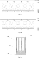
- Fig. 1a is a schematic view of a lateral cross-section view of an in-cell touch screen provided by an embodiment of the invention
- Fig. 1b is a schematic view of a longitudinal cross-section view of the in-cell touch screen provided by the embodiment of the invention.
- the in-cell touch screen provided by the embodiment of the invention includes an opposite substrate 100 and an array substrate 200 disposed oppositely.
- a touch electrode pattern 110 is disposed on a side of the opposite substrate 100, which side faces the array substrate 200.
- a data line 210 and a gate line 220 are disposed on a side of the array substrate 200, which side faces the opposite substrate 100, and the data line 210 and the gate line 220 intercross and are mutually insulated from each other.
- a common electrode layer 230 is disposed on a layer where the gate line 220 and the data line 210 are located. That is, the common electrode layer 230 is closer to the opposite substrate 100 than the gate line 220 and the date line 210.
- An orthographic projection of the common electrode layer 230 on the array substrate 200 covers orthographic projections of the gate line 220 and the data line 210 on the array substrate 200.
- the in-cell touch screen provided by the embodiment of the invention disposes the common electrode layer 230 above the data line 210 and the gate line 220 and below the touch electrode pattern 110, as shown in Fig. 1c .
- the gate line 220 and the date line 210 are fully covered by the common electrode layer 230.
- the shielding effect of the common electrode layer 230 can eliminate interference by display signals of the gate line 220 and the date line 210 on touch signals, and also the shielding effect of the common electrode layer 230 can eliminate interference by the touch signals of the touch electrode pattern 110 on the display signals.
- the in-cell touch screen provided by the embodiment of the invention can employ a manner of driving a display function and a touch function at the same time, and therefore avoiding various display problems and touch problems, during high resolution displaying, caused by insufficient time periods for the touch function and the display function in the time division driving manner.
- the touch screens provided by embodiments of the invention may be applied to In-Plane Switch (IPS) technology and Advanced Super Dimension Switch (ADS) technology.
- IPS In-Plane Switch
- ADS Advanced Super Dimension Switch
- FIG. 1a and Fig. 1b illustrate an example in an ADS mode. That is, in the ADS mode, a pixel electrode 240 on the array substrate 200 is disposed on a layer different from the common electrode layer 230.
- Fig. 1a and Fig. 1b illustrate the example in which the common electrode layer 230 is disposed above the pixel electrode 240.
- the pixel electrode 240 may be disposed above the common electrode 230, the description of which is omitted herein.
- the gate line 220 and the data line 210 are generally formed on different layers or on the same layer.
- the above-described touch screen provided by the embodiment of the invention may implement the touch function in accordance with the principle of mutual capacitance or the principle of self capacitance. That is, the touch electrode pattern disposed on the opposite substrate 100 may be implemented as a self capacitive electrode pattern or a mutual capacitive electrode pattern.
- Fig. 2 shows a basic structural diagram of implementing the touch function in accordance with the principle of self capacitance.
- a black matrix (BM) pattern is disposed on the side of the opposite substrate 100, which side faces the array substrate 200.
- the touch electrode pattern 110 is generally disposed in the following manner: an orthographic projection of the touch electrode pattern 110 on the opposite substrate 100 is fully located within an area where an orthographic projection of the black matrix (BM) pattern on the opposite substrate 100 is located.
- the data line 210, the gate line 220 and the common electrode layer 230 are all disposed on the array substrate 200.
- the data line 210 and the gate line 220 are provided too close to the common electrode layer 230, and thus it is inevitable to incur coupling effect, which effect causes the voltage on the common electrode layer 230 to fluctuate and in turn generates interference on the touch signals.
- the above-described in-cell touch screen provided by the embodiment of the invention as shown in Fig. 3a and Fig.
- a feedback compensation circuit 250 for providing a common electrode signal to the common electrode layer 230 is further disposed on the array substrate 200.
- the feedback compensation circuit 250 can compensate the signal fluctuation over the common electrode layer 230 due to the coupling effect, so as to relatively stabilize the signal over the common electrode layer 230.
- the feedback compensation circuit 250 comprises: a first operational amplifier OP1, a second operational amplifier OP2, a first resistor R1, a second resistor R2 and a filtering capacitor C1.
- R3 refers to a resistor in the panel.
- a positive input terminal of the first operational amplifier OP1 is connected to a common electrode signal standard voltage providing terminal "Vcom_standard", a negative input terminal is connected to an end of the first resistor R1, an output terminal is connected to a common electrode signal input terminal "Vcom_input” for the common electrode 230; the second resistor R2 is connected in parallel between the negative input terminal of the first operational amplifier OP1 and the output terminal; a positive input terminal of the second operational amplifier OP2 is connected to a common electrode signal feedback terminal "Vcom_feedback" for the common electrode 230, a negative input terminal is connected to an output end thereof, and the output terminal is connected to the other end of the first resistor R1 via the filtering capacitor C1.
- the main function of the filtering capacitor C1 is to prevent signal interference of unnecessary frequency.
- Vcom_feedback refers to a voltage value of the common electrode signal feedback terminal received by the positive terminal of the second operational amplifier
- Vcom_input refers to a voltage value applied by the output terminal of the first operational amplifier to the common electrode signal input terminals
- Vcom_standard refers to a voltage value of the common electrode signal standard voltage providing terminal received by the positive terminal of the first operational amplifier.
- the minus sign in the above equation refers to an opposite direction. That is, a direction of voltage difference between "Vcom_feedback” and “Vcom_standard” is opposite to a direction of voltage difference between "Vcom_input” and “Vcom_standard", while the ratio of the voltage differences is R1/R2, so that a negative feedback for the compensation to Vcom is generated and the coupling effect in the common electrode layer 230 is lowered.
- the ratio of R1 and R2 may be modified according to specific situation. Waveforms of signal terminals within one frame (STV) are shown in Fig. 5 .
- the common electrode signal feedback terminal "Vcom_feedback" of the common electrode layer 230 connected with the feedback compensation circuit 250 provided by the embodiment of the invention is generally disposed in an area of the common electrode layer 230 where signal latency is the largest. Therefore, it ensures that the feedback compensation circuit 250 can eliminate noise influence to a greatest extend.
- the area of the common electrode layer 230 with the largest signal latency is related to a position where the signal input terminal "Vcom_input" of the common electrode in the common electrode layer 230 is disposed.
- the common electrode signal feedback terminal "Vcom_feedback” is generally disposed at the central position of a base of the common electrode layer 230 on the side away from the feedback compensation circuit 250. Also as shown in Fig.
- the common electrode signal feedback terminal "Vcom_feedback” is disposed at a corner position, on the right side or the left side and opposite to the common electrode signal input terminals "Vcom_input", in the common electrode layer 230.
- the common electrode layer 230 fully covers the gate line 220 and the data line 210, the noise of the display signal is essentially applied on the common electrode layer 230. Therefore, a feedback signal acquired from the common electrode signal feedback terminal "Vcom_feedback" in the common electrode layer 230 essentially reflects all forms of the noise.
- the feedback signal from the common electrode signal feedback terminal "Vcom_feedback” may be configured to be calculated with the touch signal to eliminate possible existence of the noise, so that the acquired touch signal and the display signal may not interfere with each other when they operates simultaneously, which guarantees accuracy of touching.
- the in-cell touch screen provided by an embodiment of the invention further includes: a touch detection circuit 700 and a de-noise circuit 600.
- a first input terminal 601 of the de-noise circuit is configured to receive the touch signal TP of the touch electrode pattern
- a second input terminal 602 thereof is configured to receive a noise signal of the common electrode signal feedback terminal "Vcom_feedback”
- a output terminal 603 of the de-noise circuit is connected to an input terminal of the touch detection circuit 700
- the de-noise circuit 600 is configured to de-noise the received touch signal and then output the processed signal to the touch detection circuit 700.
- the de-noise circuit 600 is included in a de-noise module
- the touch detection circuit 700 is included in a touch positioning module.
- an embodiment of the invention provides a display device, including the in-cell touch screen provided by any one of the above embodiments.
- the display device may be: a cell phone, a watch, a tablet, a TV set, a display, a laptop, a digital frame, a navigator or any product or assembly with display function.
- the embodiment of the display device may be referred to any of the embodiments of the in-cell touch screen, description of which will be omitted herein.
- An in-cell touch screen and a display device disposes a touch electrode pattern on a side of an opposite substrate, which side faces an array substrate; disposes a data line and a gate line on a side of the array substrate, which side faces the opposite substrate, the data line and the gate line intercross and are mutually insulated from each other; and disposes a common electrode layer on a layer where the gate line and the data line are located; and an orthographic projection of the common electrode layer on the array substrate covers orthographic projections of the gate line and the data line on the array substrate.
- the touch screen provided by an embodiment of the invention disposes the common electrode layer above the gate line and the data line and below the touch electrode, and the common electrode layer fully covers the gate line and the data line, so that the shielding effect of the common electrode layer eliminates interference of display signals of the gate line and the date line on touch signals, and also the shielding effect of the common electrode layer eliminates interference of the touch signals of the touch electrode pattern on the display signals.
- the touch screen provided by the embodiments of the invention can employ a manner of driving a display function and a touch function at the same time, avoiding various display problems and touch problems during high resolution displaying caused by insufficient time periods for the touch function and the display function in a time division driving manner.
Landscapes
- Engineering & Computer Science (AREA)
- Theoretical Computer Science (AREA)
- General Engineering & Computer Science (AREA)
- Physics & Mathematics (AREA)
- General Physics & Mathematics (AREA)
- Human Computer Interaction (AREA)
- Crystallography & Structural Chemistry (AREA)
- Nonlinear Science (AREA)
- Chemical & Material Sciences (AREA)
- Optics & Photonics (AREA)
- Mathematical Physics (AREA)
- Power Engineering (AREA)
- Computer Hardware Design (AREA)
- Position Input By Displaying (AREA)
Applications Claiming Priority (2)
| Application Number | Priority Date | Filing Date | Title |
|---|---|---|---|
| CN201410540073.XA CN104281352B (zh) | 2014-10-13 | 2014-10-13 | 一种内嵌式触摸屏及显示装置 |
| PCT/CN2015/075221 WO2016058337A1 (fr) | 2014-10-13 | 2015-03-27 | Écran tactile en cellule et appareil d'affichage |
Publications (3)
| Publication Number | Publication Date |
|---|---|
| EP3208701A1 true EP3208701A1 (fr) | 2017-08-23 |
| EP3208701A4 EP3208701A4 (fr) | 2018-05-30 |
| EP3208701B1 EP3208701B1 (fr) | 2020-09-16 |
Family
ID=52256288
Family Applications (1)
| Application Number | Title | Priority Date | Filing Date |
|---|---|---|---|
| EP15763181.3A Not-in-force EP3208701B1 (fr) | 2014-10-13 | 2015-03-27 | Écran tactile en cellule et appareil d'affichage |
Country Status (4)
| Country | Link |
|---|---|
| US (1) | US10156942B2 (fr) |
| EP (1) | EP3208701B1 (fr) |
| CN (1) | CN104281352B (fr) |
| WO (1) | WO2016058337A1 (fr) |
Families Citing this family (21)
| Publication number | Priority date | Publication date | Assignee | Title |
|---|---|---|---|---|
| CN104281352B (zh) | 2014-10-13 | 2017-06-06 | 京东方科技集团股份有限公司 | 一种内嵌式触摸屏及显示装置 |
| KR102335818B1 (ko) * | 2014-12-22 | 2021-12-06 | 엘지디스플레이 주식회사 | 액정표시장치 |
| CN104571720B (zh) | 2015-02-06 | 2017-07-07 | 京东方科技集团股份有限公司 | 一种阵列基板、内嵌式触摸面板和显示装置 |
| WO2016189426A1 (fr) * | 2015-05-28 | 2016-12-01 | 株式会社半導体エネルギー研究所 | Panneau tactile |
| CN104834406B (zh) | 2015-05-29 | 2018-09-18 | 京东方科技集团股份有限公司 | 一种集成触摸功能的显示装置及其驱动方法 |
| TWI552053B (zh) * | 2015-12-31 | 2016-10-01 | 速博思股份有限公司 | 具金屬網格遮蔽層之內嵌式觸控顯示面板結構 |
| CN106125977B (zh) * | 2016-06-21 | 2019-04-23 | 上海中航光电子有限公司 | 一种触控显示面板及显示装置 |
| CN107885366B (zh) * | 2016-09-30 | 2020-12-29 | 深圳深微创芯科技有限公司 | 触摸显示装置和电子设备 |
| WO2018058664A1 (fr) * | 2016-09-30 | 2018-04-05 | 深圳深微创芯科技有限公司 | Dispositif électronique |
| WO2018058661A1 (fr) * | 2016-09-30 | 2018-04-05 | 深圳深微创芯科技有限公司 | Circuit d'attaque |
| CN209803750U (zh) * | 2016-09-30 | 2019-12-17 | 深圳深微创芯科技有限公司 | 驱动电路 |
| KR102617273B1 (ko) | 2016-10-31 | 2023-12-21 | 엘지디스플레이 주식회사 | 인셀 터치 표시 장치 |
| JP2019090939A (ja) * | 2017-11-15 | 2019-06-13 | シャープ株式会社 | アクティブマトリックス基板、表示装置、および制御方法 |
| KR102490043B1 (ko) * | 2018-08-24 | 2023-01-17 | 엘지디스플레이 주식회사 | 인셀 터치 표시 장치 |
| CN109062444B (zh) * | 2018-09-04 | 2023-04-18 | 京东方科技集团股份有限公司 | 触控显示面板及显示器 |
| US11367390B2 (en) * | 2018-12-24 | 2022-06-21 | Novatek Microelectronics Corp. | Display apparatus and method for noise reduction |
| JP7289781B2 (ja) * | 2019-12-19 | 2023-06-12 | アルパイン株式会社 | 液晶表示装置 |
| KR102890658B1 (ko) * | 2020-03-12 | 2025-11-25 | 삼성디스플레이 주식회사 | 표시 장치 |
| CN111459338A (zh) | 2020-04-13 | 2020-07-28 | 深圳市华星光电半导体显示技术有限公司 | 一种触控显示器及其抗干扰方法 |
| CN111965878B (zh) * | 2020-08-31 | 2023-06-13 | 上海天马微电子有限公司 | 调光面板及其制作方法及智能窗玻璃 |
| CN114047836A (zh) * | 2021-11-02 | 2022-02-15 | 云谷(固安)科技有限公司 | 一种显示装置 |
Family Cites Families (30)
| Publication number | Priority date | Publication date | Assignee | Title |
|---|---|---|---|---|
| JP4019697B2 (ja) * | 2001-11-15 | 2007-12-12 | 株式会社日立製作所 | 液晶表示装置 |
| JP3891846B2 (ja) * | 2002-01-15 | 2007-03-14 | 株式会社日立製作所 | 液晶表示装置 |
| JP2003295207A (ja) * | 2002-03-29 | 2003-10-15 | Nec Lcd Technologies Ltd | 横電界方式のアクティブマトリクス型液晶表示装置 |
| KR100900548B1 (ko) * | 2002-12-17 | 2009-06-02 | 삼성전자주식회사 | 크기가 다른 공통 전압을 생성하는 액정 표시 장치 |
| KR100958246B1 (ko) * | 2003-11-26 | 2010-05-17 | 엘지디스플레이 주식회사 | 횡전계 방식의 액정표시장치 및 그 제조방법 |
| KR101182322B1 (ko) * | 2006-06-30 | 2012-09-20 | 엘지디스플레이 주식회사 | 수평 전계 인가형 박막 트랜지스터 기판 및 그 제조 방법 |
| JP5093725B2 (ja) * | 2007-10-29 | 2012-12-12 | Nltテクノロジー株式会社 | 液晶表示装置 |
| JP5172508B2 (ja) * | 2008-07-09 | 2013-03-27 | 株式会社ジャパンディスプレイセントラル | 液晶表示装置 |
| KR101513271B1 (ko) | 2008-10-30 | 2015-04-17 | 삼성디스플레이 주식회사 | 표시장치 |
| KR101641982B1 (ko) * | 2009-02-09 | 2016-07-25 | 삼성디스플레이 주식회사 | 표시 장치 |
| KR101394937B1 (ko) * | 2010-09-07 | 2014-05-15 | 엘지디스플레이 주식회사 | 터치 센서를 갖는 표시 장치 및 그 방법 |
| KR101230196B1 (ko) * | 2010-10-29 | 2013-02-06 | 삼성디스플레이 주식회사 | 터치 스크린 패널 내장형 액정표시장치 |
| JP5645203B2 (ja) * | 2010-11-25 | 2014-12-24 | 三菱電機株式会社 | 液晶表示パネル及び液晶表示装置 |
| KR101329461B1 (ko) | 2010-11-25 | 2013-11-15 | 엘지디스플레이 주식회사 | 터치 스크린 패널 일체형 표시장치 |
| TWI402731B (zh) * | 2010-12-14 | 2013-07-21 | Au Optronics Corp | 觸控面板及降低觸控面板上共同電壓耦合的雜訊的方法 |
| KR101706242B1 (ko) * | 2011-04-27 | 2017-02-14 | 엘지디스플레이 주식회사 | 인셀 터치 패널 |
| KR101529557B1 (ko) * | 2011-06-09 | 2015-06-19 | 엘지디스플레이 주식회사 | 프린지 필드형 액정표시장치의 제조방법 |
| CN103163671B (zh) * | 2011-12-14 | 2016-04-20 | 上海天马微电子有限公司 | 显示面板及其形成方法、液晶显示装置 |
| JP5875001B2 (ja) * | 2012-03-14 | 2016-03-02 | Nltテクノロジー株式会社 | 横電界方式の液晶表示装置 |
| KR101871667B1 (ko) * | 2012-03-16 | 2018-06-27 | 엘지디스플레이 주식회사 | 터치스크린 연결용 연성인쇄회로기판 및 이를 이용한 액정표시장치 |
| JP5941756B2 (ja) * | 2012-06-06 | 2016-06-29 | 株式会社ジャパンディスプレイ | 液晶表示装置 |
| KR101448498B1 (ko) * | 2012-06-13 | 2014-10-08 | 엘지디스플레이 주식회사 | 터치 스크린 일체형 표시장치 |
| KR101977592B1 (ko) * | 2012-07-24 | 2019-05-13 | 엘지디스플레이 주식회사 | 공통전압 보상회로를 포함하는 액정표시장치 |
| JP6187928B2 (ja) * | 2012-09-07 | 2017-08-30 | Tianma Japan株式会社 | 横電界方式の液晶表示装置 |
| KR101555967B1 (ko) * | 2013-02-22 | 2015-09-25 | 엘지디스플레이 주식회사 | 터치스크린 일체형 표시장치 및 그 구동 방법 |
| TW201447450A (zh) * | 2013-06-07 | 2014-12-16 | Chunghwa Picture Tubes Ltd | 觸控顯示面板及其製造方法 |
| CN104122690A (zh) * | 2013-08-23 | 2014-10-29 | 深超光电(深圳)有限公司 | 液晶显示装置以及显示装置 |
| CN103760708B (zh) * | 2014-01-09 | 2017-08-11 | 北京京东方光电科技有限公司 | 一种阵列基板、电容式触摸屏和触控显示装置 |
| CN103838430B (zh) | 2014-02-24 | 2017-01-11 | 北京京东方光电科技有限公司 | 一种内嵌式触摸屏及显示装置 |
| CN104281352B (zh) | 2014-10-13 | 2017-06-06 | 京东方科技集团股份有限公司 | 一种内嵌式触摸屏及显示装置 |
-
2014
- 2014-10-13 CN CN201410540073.XA patent/CN104281352B/zh active Active
-
2015
- 2015-03-27 US US14/787,384 patent/US10156942B2/en active Active
- 2015-03-27 EP EP15763181.3A patent/EP3208701B1/fr not_active Not-in-force
- 2015-03-27 WO PCT/CN2015/075221 patent/WO2016058337A1/fr not_active Ceased
Also Published As
| Publication number | Publication date |
|---|---|
| CN104281352B (zh) | 2017-06-06 |
| WO2016058337A1 (fr) | 2016-04-21 |
| EP3208701B1 (fr) | 2020-09-16 |
| US20160195956A1 (en) | 2016-07-07 |
| US10156942B2 (en) | 2018-12-18 |
| EP3208701A4 (fr) | 2018-05-30 |
| CN104281352A (zh) | 2015-01-14 |
Similar Documents
| Publication | Publication Date | Title |
|---|---|---|
| EP3208701B1 (fr) | Écran tactile en cellule et appareil d'affichage | |
| US9823788B2 (en) | Capacitive in-cell touch panel, display device, and driving method | |
| CN103576360B (zh) | 带触摸传感器的液晶显示装置以及电子设备 | |
| CN107122087B (zh) | 带有触摸传感器的显示装置 | |
| CN107272921B (zh) | 有源触控笔、包括其的触摸感测系统和触摸感测方法 | |
| US9939938B2 (en) | Display panel with touch detecting and display device | |
| KR102045808B1 (ko) | 터치센서 일체형 표시장치 | |
| EP3038097B1 (fr) | Dispositif d'affichage avec capteur tactile | |
| JP6103650B2 (ja) | タッチセンサ一体型表示装置 | |
| KR102045809B1 (ko) | 터치센서 일체형 표시장치 | |
| US9785276B2 (en) | Capacitive in-cell touch panel and display device | |
| KR20130116425A (ko) | 터치스크린 연결용 연성인쇄회로기판 및 이를 이용한 액정표시장치 | |
| EP3316099A1 (fr) | Écran tactile incorporé et dispositif d'affichage | |
| US10627958B2 (en) | Driving method and driving device for touch panel | |
| US20160334660A1 (en) | In-cell touch panel | |
| US20180113542A1 (en) | Plug-In Touch Display Device And An Electronic Device | |
| CN203480490U (zh) | 一种电容式内嵌触摸屏及显示装置 | |
| WO2017219425A1 (fr) | Écran d'affichage à commande tactile et dispositif électronique | |
| US20180364511A1 (en) | Liquid crystal panel having touch sensor function | |
| JP6334157B2 (ja) | タッチセンサ内蔵型表示装置およびその駆動方法 | |
| KR102478670B1 (ko) | 터치 센서를 갖는 전자장치와 이의 구동 방법 | |
| CN103869525B (zh) | 触摸传感器集成式显示装置 | |
| JPH08328739A (ja) | 座標検出機能付き表示装置 |
Legal Events
| Date | Code | Title | Description |
|---|---|---|---|
| STAA | Information on the status of an ep patent application or granted ep patent |
Free format text: STATUS: THE INTERNATIONAL PUBLICATION HAS BEEN MADE |
|
| PUAI | Public reference made under article 153(3) epc to a published international application that has entered the european phase |
Free format text: ORIGINAL CODE: 0009012 |
|
| STAA | Information on the status of an ep patent application or granted ep patent |
Free format text: STATUS: REQUEST FOR EXAMINATION WAS MADE |
|
| 17P | Request for examination filed |
Effective date: 20150922 |
|
| AK | Designated contracting states |
Kind code of ref document: A1 Designated state(s): AL AT BE BG CH CY CZ DE DK EE ES FI FR GB GR HR HU IE IS IT LI LT LU LV MC MK MT NL NO PL PT RO RS SE SI SK SM TR |
|
| AX | Request for extension of the european patent |
Extension state: BA ME |
|
| DAV | Request for validation of the european patent (deleted) | ||
| DAX | Request for extension of the european patent (deleted) | ||
| A4 | Supplementary search report drawn up and despatched |
Effective date: 20180503 |
|
| RIC1 | Information provided on ipc code assigned before grant |
Ipc: G09G 3/36 20060101ALI20180425BHEP Ipc: G06F 3/044 20060101AFI20180425BHEP Ipc: G06F 3/041 20060101ALI20180425BHEP |
|
| STAA | Information on the status of an ep patent application or granted ep patent |
Free format text: STATUS: EXAMINATION IS IN PROGRESS |
|
| 17Q | First examination report despatched |
Effective date: 20191001 |
|
| REG | Reference to a national code |
Ref country code: DE Ref legal event code: R079 Ref document number: 602015059185 Country of ref document: DE Free format text: PREVIOUS MAIN CLASS: G06F0003044000 Ipc: G06F0003041000 |
|
| GRAJ | Information related to disapproval of communication of intention to grant by the applicant or resumption of examination proceedings by the epo deleted |
Free format text: ORIGINAL CODE: EPIDOSDIGR1 |
|
| GRAP | Despatch of communication of intention to grant a patent |
Free format text: ORIGINAL CODE: EPIDOSNIGR1 |
|
| GRAP | Despatch of communication of intention to grant a patent |
Free format text: ORIGINAL CODE: EPIDOSNIGR1 |
|
| STAA | Information on the status of an ep patent application or granted ep patent |
Free format text: STATUS: GRANT OF PATENT IS INTENDED |
|
| RIC1 | Information provided on ipc code assigned before grant |
Ipc: G06F 3/044 20060101ALI20200302BHEP Ipc: G06F 3/041 20060101AFI20200302BHEP Ipc: G09G 3/36 20060101ALI20200302BHEP |
|
| INTG | Intention to grant announced |
Effective date: 20200324 |
|
| GRAS | Grant fee paid |
Free format text: ORIGINAL CODE: EPIDOSNIGR3 |
|
| GRAA | (expected) grant |
Free format text: ORIGINAL CODE: 0009210 |
|
| STAA | Information on the status of an ep patent application or granted ep patent |
Free format text: STATUS: THE PATENT HAS BEEN GRANTED |
|
| AK | Designated contracting states |
Kind code of ref document: B1 Designated state(s): AL AT BE BG CH CY CZ DE DK EE ES FI FR GB GR HR HU IE IS IT LI LT LU LV MC MK MT NL NO PL PT RO RS SE SI SK SM TR |
|
| REG | Reference to a national code |
Ref country code: GB Ref legal event code: FG4D |
|
| REG | Reference to a national code |
Ref country code: CH Ref legal event code: EP |
|
| REG | Reference to a national code |
Ref country code: DE Ref legal event code: R096 Ref document number: 602015059185 Country of ref document: DE |
|
| REG | Reference to a national code |
Ref country code: IE Ref legal event code: FG4D |
|
| REG | Reference to a national code |
Ref country code: AT Ref legal event code: REF Ref document number: 1314731 Country of ref document: AT Kind code of ref document: T Effective date: 20201015 |
|
| PG25 | Lapsed in a contracting state [announced via postgrant information from national office to epo] |
Ref country code: SE Free format text: LAPSE BECAUSE OF FAILURE TO SUBMIT A TRANSLATION OF THE DESCRIPTION OR TO PAY THE FEE WITHIN THE PRESCRIBED TIME-LIMIT Effective date: 20200916 Ref country code: BG Free format text: LAPSE BECAUSE OF FAILURE TO SUBMIT A TRANSLATION OF THE DESCRIPTION OR TO PAY THE FEE WITHIN THE PRESCRIBED TIME-LIMIT Effective date: 20201216 Ref country code: HR Free format text: LAPSE BECAUSE OF FAILURE TO SUBMIT A TRANSLATION OF THE DESCRIPTION OR TO PAY THE FEE WITHIN THE PRESCRIBED TIME-LIMIT Effective date: 20200916 Ref country code: GR Free format text: LAPSE BECAUSE OF FAILURE TO SUBMIT A TRANSLATION OF THE DESCRIPTION OR TO PAY THE FEE WITHIN THE PRESCRIBED TIME-LIMIT Effective date: 20201217 Ref country code: NO Free format text: LAPSE BECAUSE OF FAILURE TO SUBMIT A TRANSLATION OF THE DESCRIPTION OR TO PAY THE FEE WITHIN THE PRESCRIBED TIME-LIMIT Effective date: 20201216 Ref country code: FI Free format text: LAPSE BECAUSE OF FAILURE TO SUBMIT A TRANSLATION OF THE DESCRIPTION OR TO PAY THE FEE WITHIN THE PRESCRIBED TIME-LIMIT Effective date: 20200916 |
|
| REG | Reference to a national code |
Ref country code: AT Ref legal event code: MK05 Ref document number: 1314731 Country of ref document: AT Kind code of ref document: T Effective date: 20200916 |
|
| REG | Reference to a national code |
Ref country code: NL Ref legal event code: MP Effective date: 20200916 |
|
| PG25 | Lapsed in a contracting state [announced via postgrant information from national office to epo] |
Ref country code: LV Free format text: LAPSE BECAUSE OF FAILURE TO SUBMIT A TRANSLATION OF THE DESCRIPTION OR TO PAY THE FEE WITHIN THE PRESCRIBED TIME-LIMIT Effective date: 20200916 Ref country code: RS Free format text: LAPSE BECAUSE OF FAILURE TO SUBMIT A TRANSLATION OF THE DESCRIPTION OR TO PAY THE FEE WITHIN THE PRESCRIBED TIME-LIMIT Effective date: 20200916 |
|
| REG | Reference to a national code |
Ref country code: LT Ref legal event code: MG4D |
|
| PG25 | Lapsed in a contracting state [announced via postgrant information from national office to epo] |
Ref country code: CZ Free format text: LAPSE BECAUSE OF FAILURE TO SUBMIT A TRANSLATION OF THE DESCRIPTION OR TO PAY THE FEE WITHIN THE PRESCRIBED TIME-LIMIT Effective date: 20200916 Ref country code: LT Free format text: LAPSE BECAUSE OF FAILURE TO SUBMIT A TRANSLATION OF THE DESCRIPTION OR TO PAY THE FEE WITHIN THE PRESCRIBED TIME-LIMIT Effective date: 20200916 Ref country code: EE Free format text: LAPSE BECAUSE OF FAILURE TO SUBMIT A TRANSLATION OF THE DESCRIPTION OR TO PAY THE FEE WITHIN THE PRESCRIBED TIME-LIMIT Effective date: 20200916 Ref country code: RO Free format text: LAPSE BECAUSE OF FAILURE TO SUBMIT A TRANSLATION OF THE DESCRIPTION OR TO PAY THE FEE WITHIN THE PRESCRIBED TIME-LIMIT Effective date: 20200916 Ref country code: SM Free format text: LAPSE BECAUSE OF FAILURE TO SUBMIT A TRANSLATION OF THE DESCRIPTION OR TO PAY THE FEE WITHIN THE PRESCRIBED TIME-LIMIT Effective date: 20200916 Ref country code: PT Free format text: LAPSE BECAUSE OF FAILURE TO SUBMIT A TRANSLATION OF THE DESCRIPTION OR TO PAY THE FEE WITHIN THE PRESCRIBED TIME-LIMIT Effective date: 20210118 |
|
| PG25 | Lapsed in a contracting state [announced via postgrant information from national office to epo] |
Ref country code: ES Free format text: LAPSE BECAUSE OF FAILURE TO SUBMIT A TRANSLATION OF THE DESCRIPTION OR TO PAY THE FEE WITHIN THE PRESCRIBED TIME-LIMIT Effective date: 20200916 Ref country code: AL Free format text: LAPSE BECAUSE OF FAILURE TO SUBMIT A TRANSLATION OF THE DESCRIPTION OR TO PAY THE FEE WITHIN THE PRESCRIBED TIME-LIMIT Effective date: 20200916 Ref country code: AT Free format text: LAPSE BECAUSE OF FAILURE TO SUBMIT A TRANSLATION OF THE DESCRIPTION OR TO PAY THE FEE WITHIN THE PRESCRIBED TIME-LIMIT Effective date: 20200916 Ref country code: PL Free format text: LAPSE BECAUSE OF FAILURE TO SUBMIT A TRANSLATION OF THE DESCRIPTION OR TO PAY THE FEE WITHIN THE PRESCRIBED TIME-LIMIT Effective date: 20200916 Ref country code: IS Free format text: LAPSE BECAUSE OF FAILURE TO SUBMIT A TRANSLATION OF THE DESCRIPTION OR TO PAY THE FEE WITHIN THE PRESCRIBED TIME-LIMIT Effective date: 20210116 |
|
| REG | Reference to a national code |
Ref country code: DE Ref legal event code: R097 Ref document number: 602015059185 Country of ref document: DE |
|
| PG25 | Lapsed in a contracting state [announced via postgrant information from national office to epo] |
Ref country code: SK Free format text: LAPSE BECAUSE OF FAILURE TO SUBMIT A TRANSLATION OF THE DESCRIPTION OR TO PAY THE FEE WITHIN THE PRESCRIBED TIME-LIMIT Effective date: 20200916 |
|
| PLBE | No opposition filed within time limit |
Free format text: ORIGINAL CODE: 0009261 |
|
| STAA | Information on the status of an ep patent application or granted ep patent |
Free format text: STATUS: NO OPPOSITION FILED WITHIN TIME LIMIT |
|
| 26N | No opposition filed |
Effective date: 20210617 |
|
| PG25 | Lapsed in a contracting state [announced via postgrant information from national office to epo] |
Ref country code: SI Free format text: LAPSE BECAUSE OF FAILURE TO SUBMIT A TRANSLATION OF THE DESCRIPTION OR TO PAY THE FEE WITHIN THE PRESCRIBED TIME-LIMIT Effective date: 20200916 Ref country code: DK Free format text: LAPSE BECAUSE OF FAILURE TO SUBMIT A TRANSLATION OF THE DESCRIPTION OR TO PAY THE FEE WITHIN THE PRESCRIBED TIME-LIMIT Effective date: 20200916 |
|
| PG25 | Lapsed in a contracting state [announced via postgrant information from national office to epo] |
Ref country code: MC Free format text: LAPSE BECAUSE OF FAILURE TO SUBMIT A TRANSLATION OF THE DESCRIPTION OR TO PAY THE FEE WITHIN THE PRESCRIBED TIME-LIMIT Effective date: 20200916 Ref country code: IT Free format text: LAPSE BECAUSE OF FAILURE TO SUBMIT A TRANSLATION OF THE DESCRIPTION OR TO PAY THE FEE WITHIN THE PRESCRIBED TIME-LIMIT Effective date: 20200916 |
|
| REG | Reference to a national code |
Ref country code: CH Ref legal event code: PL |
|
| GBPC | Gb: european patent ceased through non-payment of renewal fee |
Effective date: 20210327 |
|
| REG | Reference to a national code |
Ref country code: BE Ref legal event code: MM Effective date: 20210331 |
|
| PG25 | Lapsed in a contracting state [announced via postgrant information from national office to epo] |
Ref country code: CH Free format text: LAPSE BECAUSE OF NON-PAYMENT OF DUE FEES Effective date: 20210331 Ref country code: LU Free format text: LAPSE BECAUSE OF NON-PAYMENT OF DUE FEES Effective date: 20210327 Ref country code: LI Free format text: LAPSE BECAUSE OF NON-PAYMENT OF DUE FEES Effective date: 20210331 Ref country code: IE Free format text: LAPSE BECAUSE OF NON-PAYMENT OF DUE FEES Effective date: 20210327 Ref country code: GB Free format text: LAPSE BECAUSE OF NON-PAYMENT OF DUE FEES Effective date: 20210327 Ref country code: FR Free format text: LAPSE BECAUSE OF NON-PAYMENT OF DUE FEES Effective date: 20210331 |
|
| PG25 | Lapsed in a contracting state [announced via postgrant information from national office to epo] |
Ref country code: BE Free format text: LAPSE BECAUSE OF NON-PAYMENT OF DUE FEES Effective date: 20210331 |
|
| PG25 | Lapsed in a contracting state [announced via postgrant information from national office to epo] |
Ref country code: HU Free format text: LAPSE BECAUSE OF FAILURE TO SUBMIT A TRANSLATION OF THE DESCRIPTION OR TO PAY THE FEE WITHIN THE PRESCRIBED TIME-LIMIT; INVALID AB INITIO Effective date: 20150327 |
|
| PGFP | Annual fee paid to national office [announced via postgrant information from national office to epo] |
Ref country code: DE Payment date: 20230321 Year of fee payment: 9 |
|
| PG25 | Lapsed in a contracting state [announced via postgrant information from national office to epo] |
Ref country code: NL Free format text: LAPSE BECAUSE OF NON-PAYMENT OF DUE FEES Effective date: 20200923 Ref country code: CY Free format text: LAPSE BECAUSE OF FAILURE TO SUBMIT A TRANSLATION OF THE DESCRIPTION OR TO PAY THE FEE WITHIN THE PRESCRIBED TIME-LIMIT Effective date: 20200916 |
|
| PG25 | Lapsed in a contracting state [announced via postgrant information from national office to epo] |
Ref country code: MK Free format text: LAPSE BECAUSE OF FAILURE TO SUBMIT A TRANSLATION OF THE DESCRIPTION OR TO PAY THE FEE WITHIN THE PRESCRIBED TIME-LIMIT Effective date: 20200916 |
|
| PG25 | Lapsed in a contracting state [announced via postgrant information from national office to epo] |
Ref country code: TR Free format text: LAPSE BECAUSE OF FAILURE TO SUBMIT A TRANSLATION OF THE DESCRIPTION OR TO PAY THE FEE WITHIN THE PRESCRIBED TIME-LIMIT Effective date: 20200916 |
|
| PG25 | Lapsed in a contracting state [announced via postgrant information from national office to epo] |
Ref country code: MT Free format text: LAPSE BECAUSE OF FAILURE TO SUBMIT A TRANSLATION OF THE DESCRIPTION OR TO PAY THE FEE WITHIN THE PRESCRIBED TIME-LIMIT Effective date: 20200916 |
|
| REG | Reference to a national code |
Ref country code: DE Ref legal event code: R119 Ref document number: 602015059185 Country of ref document: DE |
|
| PG25 | Lapsed in a contracting state [announced via postgrant information from national office to epo] |
Ref country code: DE Free format text: LAPSE BECAUSE OF NON-PAYMENT OF DUE FEES Effective date: 20241001 |
|
| PG25 | Lapsed in a contracting state [announced via postgrant information from national office to epo] |
Ref country code: DE Free format text: LAPSE BECAUSE OF NON-PAYMENT OF DUE FEES Effective date: 20241001 |