EP3208748A2 - Circuit de commutation d'alimentation - Google Patents
Circuit de commutation d'alimentation Download PDFInfo
- Publication number
- EP3208748A2 EP3208748A2 EP16163854.9A EP16163854A EP3208748A2 EP 3208748 A2 EP3208748 A2 EP 3208748A2 EP 16163854 A EP16163854 A EP 16163854A EP 3208748 A2 EP3208748 A2 EP 3208748A2
- Authority
- EP
- European Patent Office
- Prior art keywords
- voltage
- circuit
- power switching
- switching circuit
- supply
- Prior art date
- Legal status (The legal status is an assumption and is not a legal conclusion. Google has not performed a legal analysis and makes no representation as to the accuracy of the status listed.)
- Granted
Links
Images

Classifications
-
- H—ELECTRICITY
- H03—ELECTRONIC CIRCUITRY
- H03K—PULSE TECHNIQUE
- H03K17/00—Electronic switching or gating, i.e. not by contact-making and –breaking
- H03K17/22—Modifications for ensuring a predetermined initial state when the supply voltage has been applied
- H03K17/223—Modifications for ensuring a predetermined initial state when the supply voltage has been applied in field-effect transistor switches
-
- H—ELECTRICITY
- H02—GENERATION; CONVERSION OR DISTRIBUTION OF ELECTRIC POWER
- H02M—APPARATUS FOR CONVERSION BETWEEN AC AND AC, BETWEEN AC AND DC, OR BETWEEN DC AND DC, AND FOR USE WITH MAINS OR SIMILAR POWER SUPPLY SYSTEMS; CONVERSION OF DC OR AC INPUT POWER INTO SURGE OUTPUT POWER; CONTROL OR REGULATION THEREOF
- H02M1/00—Details of apparatus for conversion
- H02M1/10—Arrangements incorporating converting means for enabling loads to be operated at will from different kinds of power supplies, e.g. from AC or DC
-
- G—PHYSICS
- G06—COMPUTING OR CALCULATING; COUNTING
- G06K—GRAPHICAL DATA READING; PRESENTATION OF DATA; RECORD CARRIERS; HANDLING RECORD CARRIERS
- G06K19/00—Record carriers for use with machines and with at least a part designed to carry digital markings
- G06K19/06—Record carriers for use with machines and with at least a part designed to carry digital markings characterised by the kind of the digital marking, e.g. shape, nature, code
- G06K19/067—Record carriers with conductive marks, printed circuits or semiconductor circuit elements, e.g. credit or identity cards also with resonating or responding marks without active components
- G06K19/07—Record carriers with conductive marks, printed circuits or semiconductor circuit elements, e.g. credit or identity cards also with resonating or responding marks without active components with integrated circuit chips
- G06K19/0701—Record carriers with conductive marks, printed circuits or semiconductor circuit elements, e.g. credit or identity cards also with resonating or responding marks without active components with integrated circuit chips at least one of the integrated circuit chips comprising an arrangement for power management
-
- G—PHYSICS
- G05—CONTROLLING; REGULATING
- G05F—SYSTEMS FOR REGULATING ELECTRIC OR MAGNETIC VARIABLES
- G05F3/00—Non-retroactive systems for regulating electric variables by using an uncontrolled element, or an uncontrolled combination of elements, such element or such combination having self-regulating properties
- G05F3/02—Regulating voltage or current
- G05F3/08—Regulating voltage or current wherein the variable is DC
-
- G—PHYSICS
- G06—COMPUTING OR CALCULATING; COUNTING
- G06K—GRAPHICAL DATA READING; PRESENTATION OF DATA; RECORD CARRIERS; HANDLING RECORD CARRIERS
- G06K19/00—Record carriers for use with machines and with at least a part designed to carry digital markings
- G06K19/06—Record carriers for use with machines and with at least a part designed to carry digital markings characterised by the kind of the digital marking, e.g. shape, nature, code
- G06K19/067—Record carriers with conductive marks, printed circuits or semiconductor circuit elements, e.g. credit or identity cards also with resonating or responding marks without active components
- G06K19/07—Record carriers with conductive marks, printed circuits or semiconductor circuit elements, e.g. credit or identity cards also with resonating or responding marks without active components with integrated circuit chips
- G06K19/0723—Record carriers with conductive marks, printed circuits or semiconductor circuit elements, e.g. credit or identity cards also with resonating or responding marks without active components with integrated circuit chips the record carrier comprising an arrangement for non-contact communication, e.g. wireless communication circuits on transponder cards, non-contact smart cards or RFIDs
Definitions
- the present disclosure relates to a power switching circuit. Furthermore, the present disclosure relates to a corresponding method of operating a power switching circuit.
- Certain devices such as NFC or RFID tags, may have two or more interfaces.
- these devices may have a contact interface.
- An example of such a device is a dual-interface NFC tag compliant with the NFC Forum standards.
- a power switching circuit comprising: a bandgap reference circuit (BGR) configured to receive an input voltage and to generate a reference voltage in response to receiving said input voltage; a supply selection circuit configured to receive at least two supply voltages, to select the highest voltage of said supply voltages and to provide said highest voltage to the bandgap reference circuit.
- BGR bandgap reference circuit
- a first supply voltage is derived from an RF input of said power switching circuit.
- a second supply voltage is derived from a contact-interface input of said power switching circuit.
- the power switching circuit further comprises a voltage blocking circuit configured to block the second supply voltage if said second supply voltage is below a threshold.
- the power switching circuit further comprises a plurality of power switches for facilitating switching between the supply voltages, and the voltage blocking circuit is configured to prevent said power switches from receiving the second supply voltage if said second supply voltage is below the threshold.
- the voltage blocking circuit is a power-on reset circuit (POR).
- POR power-on reset circuit
- the supply selection circuit comprises a first stage and a second stage, the first stage is configured to create a differential voltage from input currents induced by the supply voltages, and the second stage is configured to amplify said differential voltage and to switch the maximum of the supply voltages to an output voltage.
- a NFC/RFID tag circuit comprises the power switching circuit of the kind set forth, a contactless interface and a contact interface, and the contactless interface and the contact interface are configured to provide the supply voltages to the power switching circuit.
- the NFC/RFID tag circuit further comprises an output interface, and the power switching circuit is configured to provide an output voltage to an external device through said output interface.
- the output interface is an I 2 C interface.
- a method of operating a power switching circuit comprising: a bandgap reference circuit of said power switching circuit receives an input voltage and generates a reference voltage in response to receiving said input voltage; a supply selection circuit of said power switching circuit receives at least two supply voltages, selects the highest voltage of said supply voltages and provides said highest voltage to the bandgap reference circuit.
- a first supply voltage is derived from an RF input of said power switching circuit.
- a second supply voltage is derived from a contact-interface input of said power switching circuit.
- a voltage blocking circuit of said power switching circuit blocks the second supply voltage if said second supply voltage is below a threshold.
- the voltage blocking circuit prevents power switches of said power switching circuit from receiving the second supply voltage if said second supply voltage is below the threshold.
- Fig. 1 shows an example of a power switching circuit 100.
- the power switching circuit 100 comprises a power switching circuit 100, a VCC pin 102, a VOUT pin 104, a rectifier 106, a coil voltage limiter 108, a VDDA shunt regulator 110, a bandgap reference circuit 112, an I 2 C regulator 114, an FD comparator 120, power switches 122, and control gates 116, 118 of the power switches 122.
- a power switching circuit 100 of this kind is often used in dual-interface NFC or RFID tag circuit.
- dual-interface NFC or RFID tags may be supplied with power through both interfaces, and a power switching circuit may be configured to switch between the different power sources.
- Tag circuits with a dual power supply i.e. a contactless (RF) power supply and contact-based power supply (VCC) may contain a complex power switching mechanism for choosing one of these supplies for the system.
- Tag circuits of this kind may provide the energy received from the contactless or contact-based power supply to an external device (e.g., a microcontroller) through an output interface (e.g., an I 2 C interface).
- an external device e.g., a microcontroller
- an output interface e.g., an I 2 C interface
- Examples of such tag circuits are the "NTAG I 2 C” and "NTAG I 2 C Plus" devices manufactured by NXP Semiconductors. NTAG devices may operate in a so-called energy-harvesting mode in which the VCC pin can be powered from the RF field, as shown in Fig. 1 .
- the VOUT pin 104 sources constant current from a regulated supply voltage derived from the RF input.
- the VCC pin 102 is shorted to the VOUT pin 104.
- Both the I 2 C regulator 114 and the VDDA shunt regulator 110 have threshold-voltage (VTH) based, crude pre-regulators which can bring their output voltages to a value where the bandgap reference circuit 112 can be operational, once the respective input supply is turned ON. Once reference voltage builds up, the main loop in the regulators brings the output voltage (VDDAO) of the power switching circuit to a final regulated voltage.
- VDDA is the regulated supply voltage derived from the RF input
- VDDI is the regulated supply voltage derived from the contact-based power supply.
- the signal FD field detect
- FD field detect
- VDDI_OK will be high if BG_OK is high and VDDI rises above a certain threshold voltage level.
- VDDI_OK high indicates that VCC is ON and that VDDI is ready to supply the load. If FD is low (i.e., in the absence of an RF field), the gate SW1 116 will be turned ON and the gate SW2 118 will be turned OFF. VDDI passes through gate SW1 116 pulling net G1 to low.
- VDDI_OK passes to net G2.
- VCC VOUT
- VOUT VCC (VOUT) can discharge to any value depending on the RF reset duration and the current flowing through VCC.
- the circuit condition when there is no RF input and at lower VCC voltage may be as follows:
- VDDA rises partially as defined by a pre-regulator.
- VDDI network G2
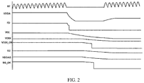
- Fig. 2 shows example waveforms for the power switching circuit of Fig. 1 .
- VDDAO doesn't rise and follows VDDI.
- FD and BG_OK remain in a logic low state.
- VDDA rises partially and remains there.
- the system may remain indefinitely in a certain state.
- a power switching circuit comprising: a bandgap reference circuit configured to receive an input voltage and to generate a reference voltage in response to receiving said input voltage, and a supply selection circuit configured to receive at least two supply voltages, to select the highest voltage of said supply voltages and to provide said highest voltage to the bandgap reference circuit.
- a bandgap reference circuit configured to receive an input voltage and to generate a reference voltage in response to receiving said input voltage
- a supply selection circuit configured to receive at least two supply voltages, to select the highest voltage of said supply voltages and to provide said highest voltage to the bandgap reference circuit.
- a second supply voltage may be derived from a contact-interface input of said power switching circuit.
- the power switching circuit includes a voltage blocking circuit configured to block the second supply voltage if said second supply voltage is below a threshold. This may also contribute to preventing that the power switching circuit is trapped in a certain state.
- the voltage blocking circuit is a power-on reset (POR) circuit.
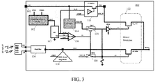
- Fig. 3 shows an illustrative embodiment of a power switching circuit 300.
- the power switching circuit 300 comprises, in addition to components shown in Fig. 1 , a maximum supply selector 302 (i.e., a supply selection circuit) and a VCC-POR circuit 304 (i.e., a voltage blocking circuit implemented as a power-on reset circuit).
- the maximum supply selector 302 is operatively coupled to the bandgap reference circuit 112. In operation, the maximum supply selector 302 receives VDDI and VDDA, selects the maximum of VDDI and VDDA, and provides said maximum to the bandgap reference circuit 112.
- the bandgap reference circuit 112 is effectively powered by the maximum of the supply voltages VDDI and VDDA, thus allowing the bandgap reference circuit 112 to start up immediately in the sense that any of the supply voltages VDDI and VDDA is promptly available to it.
- the VCC-POR circuit 304 blocks the voltage VCC if VCC is below a predefined threshold. For example, 1.2V is a suitable threshold.
- the VCC-POR circuit 304 prevents the power switches 122 from receiving VCC if VCC is below said threshold.
- the VCC-POR circuit 304 effectively blocks lower VCC voltages so that they do not enter into the power switches 122, thus making net G2 low at lower VCC voltages. This allows VDDA to pass to VDDAO upon card entering into RF field.
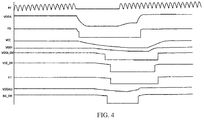
- Fig. 4 shows example waveforms for the power switching circuit of Fig. 3 .
- VDDA once RF turns ON after a reset VDDA starts rising by pre-regulator.
- the maximum supply selector switches to VDDA from VDDI once VDDA rises above the VDDI voltage.
- BG_OK is asserted HIGH (meaning that the bandgap reference circuit has started up and that the reference voltages generated by it are stable) causing VDDA to reach the state of a final regulated voltage.
- VCC voltage is low
- VCC_OK will be low, causing voltage at net G2 to be low. This allows VDDA to pass to VDDAO.
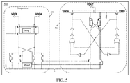
- Fig. 5 shows an illustrative embodiment of a supply selection circuit 500.
- the supply selection circuit 500 includes a first stage 502 (i.e., an input stage or comparator) and a second stage 504.
- the size of the input transistors of the comparator 502 may be properly chosen, so as to limit the current induced by the voltage VDDA.
- the minimum voltage required for the comparator 502 to operate with sufficient gain may be Vov [Overdrive voltage of Input Transistors, Minp] + VTH [Threshold of Load Transistors, Mload] ⁇ 0.8 V.
- the input stage 502 is a common-gate stage which senses voltages VDDI and VDDA and converts them to a proportional current.
- the first stage load is a hysteresis-generating cross-coupled architecture which creates a differential voltage from input currents. This differential voltage is proportional to the voltage difference between the power supplies.
- the second stage 504 amplifies this differential voltage and switches the maximum of two input voltage to VOUT. A break-before-make configuration may be implemented in the second stage 504 so as to avoid a shoot-through current while switching.
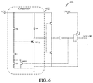
- Fig. 6 shows an illustrative embodiment of a voltage blocking circuit 600.
- the voltage blocking circuit 600 comprises a comparator 602.
- Resistors R1 and R2 define the trip voltage of the voltage blocking circuit 600 for a given size of transistor MN1 and resistor R4.
- the type of resistor R4 may be chosen carefully to counter VT variation of transistor MN1 with temperature.
- Transistor MN2 and resistor R3 introduce hysteresis.
- the output may be level shifted to VMAX.
- the presently disclosed power switching circuit may be used to advantage in NFC or RFID tag circuits, in particular in dual-interface NFC or RFID tag circuits.
- the first supply voltage may be provided by a so-called contactless interface, for example as defined in the standard ISO/IEC 14443
- the second supply voltage may be provided by a so-called contact interface, for example as defined in the standard ISO/IEC 7816.
- the tag circuit may include an output interface, for example an I 2 C interface for coupling the tag circuit to an external device (e.g., a microcontroller).
- the presently disclosed power switching circuit may be configured to provide an output voltage to this external device through said output interface.
Landscapes
- Engineering & Computer Science (AREA)
- Physics & Mathematics (AREA)
- General Physics & Mathematics (AREA)
- Computer Hardware Design (AREA)
- Microelectronics & Electronic Packaging (AREA)
- Theoretical Computer Science (AREA)
- Electromagnetism (AREA)
- Radar, Positioning & Navigation (AREA)
- Automation & Control Theory (AREA)
- Computer Networks & Wireless Communication (AREA)
- Power Engineering (AREA)
- Power Sources (AREA)
- Electronic Switches (AREA)
- Control Of Electrical Variables (AREA)
- Dc-Dc Converters (AREA)
Priority Applications (2)
| Application Number | Priority Date | Filing Date | Title |
|---|---|---|---|
| CN201710009467.6A CN107104583B (zh) | 2016-02-19 | 2017-01-05 | 电源开关电路 |
| US15/435,244 US10243554B2 (en) | 2016-02-16 | 2017-02-16 | Power switching circuit |
Applications Claiming Priority (1)
| Application Number | Priority Date | Filing Date | Title |
|---|---|---|---|
| IN201611005879 | 2016-02-19 |
Publications (3)
| Publication Number | Publication Date |
|---|---|
| EP3208748A2 true EP3208748A2 (fr) | 2017-08-23 |
| EP3208748A3 EP3208748A3 (fr) | 2017-08-30 |
| EP3208748B1 EP3208748B1 (fr) | 2019-06-12 |
Family
ID=55806132
Family Applications (1)
| Application Number | Title | Priority Date | Filing Date |
|---|---|---|---|
| EP16163854.9A Active EP3208748B1 (fr) | 2016-02-16 | 2016-04-05 | Circuit de commutation d'alimentation |
Country Status (3)
| Country | Link |
|---|---|
| US (1) | US10243554B2 (fr) |
| EP (1) | EP3208748B1 (fr) |
| CN (1) | CN107104583B (fr) |
Cited By (2)
| Publication number | Priority date | Publication date | Assignee | Title |
|---|---|---|---|---|
| CN111009955A (zh) * | 2019-11-26 | 2020-04-14 | 武汉联特科技有限公司 | 一种带保护的双电源供电电路 |
| EP4235500A1 (fr) * | 2022-02-25 | 2023-08-30 | STMicroelectronics razvoj polprevodnikov d.o.o. | Régulateur de carte ci |
Families Citing this family (6)
| Publication number | Priority date | Publication date | Assignee | Title |
|---|---|---|---|---|
| CN107995782B (zh) * | 2017-12-05 | 2020-06-09 | 晶晨半导体(上海)股份有限公司 | 一种基于cpu内部走线来优化地平面的pcb板 |
| US10411687B2 (en) * | 2018-01-03 | 2019-09-10 | Cirel Systems Private Limited | Near zero quiescent current circuit for selecting a maximum supply voltage |
| CN110148387A (zh) * | 2019-05-21 | 2019-08-20 | 合肥奕斯伟集成电路有限公司 | 一种驱动电路的输出补偿方法及系统 |
| ES3064414T3 (en) * | 2020-12-28 | 2026-04-24 | Silicon Craft Tech Public Company Limited Sict | Voltage regulator circuit for rfid circuit |
| US11728789B2 (en) * | 2021-08-19 | 2023-08-15 | Taiwan Semiconductor Manufacturing Co., Ltd. | Voltage supply selection circuit |
| KR20240114615A (ko) | 2023-01-17 | 2024-07-24 | 삼성전자주식회사 | 스마트 카드 |
Family Cites Families (11)
| Publication number | Priority date | Publication date | Assignee | Title |
|---|---|---|---|---|
| US3502905A (en) * | 1967-05-17 | 1970-03-24 | Honeywell Inc | Differential amplifier and field effect transistor gates for applying largest of two inputs to output |
| JPH08289483A (ja) * | 1995-04-18 | 1996-11-01 | Rohm Co Ltd | 電源回路 |
| FR2755316B1 (fr) * | 1996-10-25 | 1999-01-15 | Sgs Thomson Microelectronics | Regulateur de tension a selection automatique d'une tension d'alimentation la plus elevee |
| US6285091B1 (en) * | 1999-05-10 | 2001-09-04 | California Micro Devices Corporation | Voltage source switching circuit at reduced voltage drop levels |
| US7446434B1 (en) * | 2000-04-07 | 2008-11-04 | Motorola, Inc. | Dual mode power management system |
| US8013473B2 (en) * | 2006-09-01 | 2011-09-06 | Atmel Corporation | Detector based combination regulator |
| KR101349880B1 (ko) * | 2006-10-02 | 2014-01-09 | 가부시키가이샤 한도오따이 에네루기 켄큐쇼 | 반도체장치 |
| US7808387B1 (en) * | 2007-06-07 | 2010-10-05 | Impinj, Inc. | Voltage reference circuit with low-power bandgap |
| JP5258490B2 (ja) * | 2008-10-02 | 2013-08-07 | ルネサスエレクトロニクス株式会社 | 半導体集積回路及びそれを用いたicカード |
| JP5998025B2 (ja) * | 2012-11-28 | 2016-09-28 | ルネサスエレクトロニクス株式会社 | 半導体集積回路およびその動作方法 |
| CN104156757B (zh) * | 2014-06-25 | 2017-04-05 | 赵犁 | 嵌入温度传感器的无源超高频超低功耗rfid标签芯片 |
-
2016
- 2016-04-05 EP EP16163854.9A patent/EP3208748B1/fr active Active
-
2017
- 2017-01-05 CN CN201710009467.6A patent/CN107104583B/zh active Active
- 2017-02-16 US US15/435,244 patent/US10243554B2/en active Active
Non-Patent Citations (1)
| Title |
|---|
| None |
Cited By (4)
| Publication number | Priority date | Publication date | Assignee | Title |
|---|---|---|---|---|
| CN111009955A (zh) * | 2019-11-26 | 2020-04-14 | 武汉联特科技有限公司 | 一种带保护的双电源供电电路 |
| CN111009955B (zh) * | 2019-11-26 | 2021-07-09 | 武汉联特科技股份有限公司 | 一种带保护的双电源供电电路 |
| EP4235500A1 (fr) * | 2022-02-25 | 2023-08-30 | STMicroelectronics razvoj polprevodnikov d.o.o. | Régulateur de carte ci |
| US11934217B2 (en) | 2022-02-25 | 2024-03-19 | Stmicroelectronics Razvoj Polprevodnikov D.O.O. | IC card regulator |
Also Published As
| Publication number | Publication date |
|---|---|
| CN107104583B (zh) | 2020-10-20 |
| EP3208748B1 (fr) | 2019-06-12 |
| EP3208748A3 (fr) | 2017-08-30 |
| CN107104583A (zh) | 2017-08-29 |
| US10243554B2 (en) | 2019-03-26 |
| US20170244405A1 (en) | 2017-08-24 |
Similar Documents
| Publication | Publication Date | Title |
|---|---|---|
| US10243554B2 (en) | Power switching circuit | |
| CN109428575B (zh) | 用于次级供电域的通电重置系统 | |
| US8729960B2 (en) | Dynamic adjusting RFID demodulation circuit | |
| KR102714880B1 (ko) | 드라이버 및 슬루율-제어 회로 | |
| US8841890B2 (en) | Shunt regulator circuit having a split output | |
| JP6248779B2 (ja) | 電源切り替え回路、半導体集積回路、無線装置、無線システム及び電源切り替え方法 | |
| EP3136601B1 (fr) | Circuit de réinitialisation de mise sous tension | |
| CN108023581B (zh) | 小面积低功率上电复位电路 | |
| US10355477B2 (en) | Digital signal transfer between multiple voltage domains | |
| US8729874B2 (en) | Generation of voltage supply for low power digital circuit operation | |
| US8823267B2 (en) | Bandgap ready circuit | |
| US10243410B2 (en) | Electronic device and power management method | |
| US10432107B2 (en) | Rectifier circuit and electronic device | |
| US8669801B2 (en) | Analog delay cells for the power supply of an RFID tag | |
| EP1643645A1 (fr) | Circuit redresseur | |
| US8584959B2 (en) | Power-on sequencing for an RFID tag | |
| US9780647B2 (en) | Input-output circuits | |
| US6204704B1 (en) | Micropower, minimal area DC sensing power-up reset circuit | |
| US6992489B2 (en) | Multiple voltage level detection circuit | |
| JP2011188361A (ja) | パワーオンリセット回路 | |
| CN108776501B (zh) | Ldo和por的复用电路 | |
| EP4273749B1 (fr) | Limiteur de tension pour une étiquette rfid | |
| US9647456B2 (en) | Power management circuit and a method for operating a power management circuit | |
| EP4535666A1 (fr) | Circuit de remise à zéro à la mise sous tension | |
| KR101076725B1 (ko) | 전압 조정기 및 이를 이용한 rfid 장치 |
Legal Events
| Date | Code | Title | Description |
|---|---|---|---|
| PUAI | Public reference made under article 153(3) epc to a published international application that has entered the european phase |
Free format text: ORIGINAL CODE: 0009012 |
|
| STAA | Information on the status of an ep patent application or granted ep patent |
Free format text: STATUS: THE APPLICATION HAS BEEN PUBLISHED |
|
| PUAL | Search report despatched |
Free format text: ORIGINAL CODE: 0009013 |
|
| AK | Designated contracting states |
Kind code of ref document: A2 Designated state(s): AL AT BE BG CH CY CZ DE DK EE ES FI FR GB GR HR HU IE IS IT LI LT LU LV MC MK MT NL NO PL PT RO RS SE SI SK SM TR |
|
| AX | Request for extension of the european patent |
Extension state: BA ME |
|
| AK | Designated contracting states |
Kind code of ref document: A3 Designated state(s): AL AT BE BG CH CY CZ DE DK EE ES FI FR GB GR HR HU IE IS IT LI LT LU LV MC MK MT NL NO PL PT RO RS SE SI SK SM TR |
|
| AX | Request for extension of the european patent |
Extension state: BA ME |
|
| RIC1 | Information provided on ipc code assigned before grant |
Ipc: G06K 19/07 20060101AFI20170727BHEP |
|
| STAA | Information on the status of an ep patent application or granted ep patent |
Free format text: STATUS: REQUEST FOR EXAMINATION WAS MADE |
|
| 17P | Request for examination filed |
Effective date: 20180228 |
|
| RBV | Designated contracting states (corrected) |
Designated state(s): AL AT BE BG CH CY CZ DE DK EE ES FI FR GB GR HR HU IE IS IT LI LT LU LV MC MK MT NL NO PL PT RO RS SE SI SK SM TR |
|
| STAA | Information on the status of an ep patent application or granted ep patent |
Free format text: STATUS: EXAMINATION IS IN PROGRESS |
|
| 17Q | First examination report despatched |
Effective date: 20180822 |
|
| GRAP | Despatch of communication of intention to grant a patent |
Free format text: ORIGINAL CODE: EPIDOSNIGR1 |
|
| STAA | Information on the status of an ep patent application or granted ep patent |
Free format text: STATUS: GRANT OF PATENT IS INTENDED |
|
| RIC1 | Information provided on ipc code assigned before grant |
Ipc: G05F 3/08 20060101ALI20190212BHEP Ipc: G06K 19/07 20060101AFI20190212BHEP Ipc: H03K 17/22 20060101ALI20190212BHEP |
|
| INTG | Intention to grant announced |
Effective date: 20190227 |
|
| GRAS | Grant fee paid |
Free format text: ORIGINAL CODE: EPIDOSNIGR3 |
|
| GRAA | (expected) grant |
Free format text: ORIGINAL CODE: 0009210 |
|
| STAA | Information on the status of an ep patent application or granted ep patent |
Free format text: STATUS: THE PATENT HAS BEEN GRANTED |
|
| AK | Designated contracting states |
Kind code of ref document: B1 Designated state(s): AL AT BE BG CH CY CZ DE DK EE ES FI FR GB GR HR HU IE IS IT LI LT LU LV MC MK MT NL NO PL PT RO RS SE SI SK SM TR |
|
| REG | Reference to a national code |
Ref country code: GB Ref legal event code: FG4D |
|
| REG | Reference to a national code |
Ref country code: CH Ref legal event code: EP |
|
| REG | Reference to a national code |
Ref country code: AT Ref legal event code: REF Ref document number: 1143535 Country of ref document: AT Kind code of ref document: T Effective date: 20190615 |
|
| REG | Reference to a national code |
Ref country code: DE Ref legal event code: R096 Ref document number: 602016015011 Country of ref document: DE |
|
| REG | Reference to a national code |
Ref country code: IE Ref legal event code: FG4D |
|
| REG | Reference to a national code |
Ref country code: NL Ref legal event code: MP Effective date: 20190612 |
|
| REG | Reference to a national code |
Ref country code: LT Ref legal event code: MG4D |
|
| PG25 | Lapsed in a contracting state [announced via postgrant information from national office to epo] |
Ref country code: HR Free format text: LAPSE BECAUSE OF FAILURE TO SUBMIT A TRANSLATION OF THE DESCRIPTION OR TO PAY THE FEE WITHIN THE PRESCRIBED TIME-LIMIT Effective date: 20190612 Ref country code: LT Free format text: LAPSE BECAUSE OF FAILURE TO SUBMIT A TRANSLATION OF THE DESCRIPTION OR TO PAY THE FEE WITHIN THE PRESCRIBED TIME-LIMIT Effective date: 20190612 Ref country code: FI Free format text: LAPSE BECAUSE OF FAILURE TO SUBMIT A TRANSLATION OF THE DESCRIPTION OR TO PAY THE FEE WITHIN THE PRESCRIBED TIME-LIMIT Effective date: 20190612 Ref country code: NO Free format text: LAPSE BECAUSE OF FAILURE TO SUBMIT A TRANSLATION OF THE DESCRIPTION OR TO PAY THE FEE WITHIN THE PRESCRIBED TIME-LIMIT Effective date: 20190912 Ref country code: SE Free format text: LAPSE BECAUSE OF FAILURE TO SUBMIT A TRANSLATION OF THE DESCRIPTION OR TO PAY THE FEE WITHIN THE PRESCRIBED TIME-LIMIT Effective date: 20190612 Ref country code: AL Free format text: LAPSE BECAUSE OF FAILURE TO SUBMIT A TRANSLATION OF THE DESCRIPTION OR TO PAY THE FEE WITHIN THE PRESCRIBED TIME-LIMIT Effective date: 20190612 |
|
| PG25 | Lapsed in a contracting state [announced via postgrant information from national office to epo] |
Ref country code: BG Free format text: LAPSE BECAUSE OF FAILURE TO SUBMIT A TRANSLATION OF THE DESCRIPTION OR TO PAY THE FEE WITHIN THE PRESCRIBED TIME-LIMIT Effective date: 20190912 Ref country code: RS Free format text: LAPSE BECAUSE OF FAILURE TO SUBMIT A TRANSLATION OF THE DESCRIPTION OR TO PAY THE FEE WITHIN THE PRESCRIBED TIME-LIMIT Effective date: 20190612 Ref country code: LV Free format text: LAPSE BECAUSE OF FAILURE TO SUBMIT A TRANSLATION OF THE DESCRIPTION OR TO PAY THE FEE WITHIN THE PRESCRIBED TIME-LIMIT Effective date: 20190612 Ref country code: GR Free format text: LAPSE BECAUSE OF FAILURE TO SUBMIT A TRANSLATION OF THE DESCRIPTION OR TO PAY THE FEE WITHIN THE PRESCRIBED TIME-LIMIT Effective date: 20190913 |
|
| REG | Reference to a national code |
Ref country code: AT Ref legal event code: MK05 Ref document number: 1143535 Country of ref document: AT Kind code of ref document: T Effective date: 20190612 |
|
| PG25 | Lapsed in a contracting state [announced via postgrant information from national office to epo] |
Ref country code: EE Free format text: LAPSE BECAUSE OF FAILURE TO SUBMIT A TRANSLATION OF THE DESCRIPTION OR TO PAY THE FEE WITHIN THE PRESCRIBED TIME-LIMIT Effective date: 20190612 Ref country code: SK Free format text: LAPSE BECAUSE OF FAILURE TO SUBMIT A TRANSLATION OF THE DESCRIPTION OR TO PAY THE FEE WITHIN THE PRESCRIBED TIME-LIMIT Effective date: 20190612 Ref country code: AT Free format text: LAPSE BECAUSE OF FAILURE TO SUBMIT A TRANSLATION OF THE DESCRIPTION OR TO PAY THE FEE WITHIN THE PRESCRIBED TIME-LIMIT Effective date: 20190612 Ref country code: PT Free format text: LAPSE BECAUSE OF FAILURE TO SUBMIT A TRANSLATION OF THE DESCRIPTION OR TO PAY THE FEE WITHIN THE PRESCRIBED TIME-LIMIT Effective date: 20191014 Ref country code: RO Free format text: LAPSE BECAUSE OF FAILURE TO SUBMIT A TRANSLATION OF THE DESCRIPTION OR TO PAY THE FEE WITHIN THE PRESCRIBED TIME-LIMIT Effective date: 20190612 Ref country code: NL Free format text: LAPSE BECAUSE OF FAILURE TO SUBMIT A TRANSLATION OF THE DESCRIPTION OR TO PAY THE FEE WITHIN THE PRESCRIBED TIME-LIMIT Effective date: 20190612 Ref country code: CZ Free format text: LAPSE BECAUSE OF FAILURE TO SUBMIT A TRANSLATION OF THE DESCRIPTION OR TO PAY THE FEE WITHIN THE PRESCRIBED TIME-LIMIT Effective date: 20190612 |
|
| PG25 | Lapsed in a contracting state [announced via postgrant information from national office to epo] |
Ref country code: SM Free format text: LAPSE BECAUSE OF FAILURE TO SUBMIT A TRANSLATION OF THE DESCRIPTION OR TO PAY THE FEE WITHIN THE PRESCRIBED TIME-LIMIT Effective date: 20190612 Ref country code: IS Free format text: LAPSE BECAUSE OF FAILURE TO SUBMIT A TRANSLATION OF THE DESCRIPTION OR TO PAY THE FEE WITHIN THE PRESCRIBED TIME-LIMIT Effective date: 20191012 Ref country code: IT Free format text: LAPSE BECAUSE OF FAILURE TO SUBMIT A TRANSLATION OF THE DESCRIPTION OR TO PAY THE FEE WITHIN THE PRESCRIBED TIME-LIMIT Effective date: 20190612 Ref country code: ES Free format text: LAPSE BECAUSE OF FAILURE TO SUBMIT A TRANSLATION OF THE DESCRIPTION OR TO PAY THE FEE WITHIN THE PRESCRIBED TIME-LIMIT Effective date: 20190612 |
|
| REG | Reference to a national code |
Ref country code: DE Ref legal event code: R097 Ref document number: 602016015011 Country of ref document: DE |
|
| PG25 | Lapsed in a contracting state [announced via postgrant information from national office to epo] |
Ref country code: TR Free format text: LAPSE BECAUSE OF FAILURE TO SUBMIT A TRANSLATION OF THE DESCRIPTION OR TO PAY THE FEE WITHIN THE PRESCRIBED TIME-LIMIT Effective date: 20190612 |
|
| PLBE | No opposition filed within time limit |
Free format text: ORIGINAL CODE: 0009261 |
|
| STAA | Information on the status of an ep patent application or granted ep patent |
Free format text: STATUS: NO OPPOSITION FILED WITHIN TIME LIMIT |
|
| PG25 | Lapsed in a contracting state [announced via postgrant information from national office to epo] |
Ref country code: DK Free format text: LAPSE BECAUSE OF FAILURE TO SUBMIT A TRANSLATION OF THE DESCRIPTION OR TO PAY THE FEE WITHIN THE PRESCRIBED TIME-LIMIT Effective date: 20190612 Ref country code: PL Free format text: LAPSE BECAUSE OF FAILURE TO SUBMIT A TRANSLATION OF THE DESCRIPTION OR TO PAY THE FEE WITHIN THE PRESCRIBED TIME-LIMIT Effective date: 20190612 |
|
| 26N | No opposition filed |
Effective date: 20200313 |
|
| PG25 | Lapsed in a contracting state [announced via postgrant information from national office to epo] |
Ref country code: IS Free format text: LAPSE BECAUSE OF FAILURE TO SUBMIT A TRANSLATION OF THE DESCRIPTION OR TO PAY THE FEE WITHIN THE PRESCRIBED TIME-LIMIT Effective date: 20200224 Ref country code: SI Free format text: LAPSE BECAUSE OF FAILURE TO SUBMIT A TRANSLATION OF THE DESCRIPTION OR TO PAY THE FEE WITHIN THE PRESCRIBED TIME-LIMIT Effective date: 20190612 |
|
| PG2D | Information on lapse in contracting state deleted |
Ref country code: IS |
|
| PG25 | Lapsed in a contracting state [announced via postgrant information from national office to epo] |
Ref country code: MC Free format text: LAPSE BECAUSE OF FAILURE TO SUBMIT A TRANSLATION OF THE DESCRIPTION OR TO PAY THE FEE WITHIN THE PRESCRIBED TIME-LIMIT Effective date: 20190612 |
|
| REG | Reference to a national code |
Ref country code: CH Ref legal event code: PL |
|
| PG25 | Lapsed in a contracting state [announced via postgrant information from national office to epo] |
Ref country code: CH Free format text: LAPSE BECAUSE OF NON-PAYMENT OF DUE FEES Effective date: 20200430 Ref country code: LI Free format text: LAPSE BECAUSE OF NON-PAYMENT OF DUE FEES Effective date: 20200430 Ref country code: LU Free format text: LAPSE BECAUSE OF NON-PAYMENT OF DUE FEES Effective date: 20200405 |
|
| REG | Reference to a national code |
Ref country code: BE Ref legal event code: MM Effective date: 20200430 |
|
| PG25 | Lapsed in a contracting state [announced via postgrant information from national office to epo] |
Ref country code: BE Free format text: LAPSE BECAUSE OF NON-PAYMENT OF DUE FEES Effective date: 20200430 |
|
| PG25 | Lapsed in a contracting state [announced via postgrant information from national office to epo] |
Ref country code: IE Free format text: LAPSE BECAUSE OF NON-PAYMENT OF DUE FEES Effective date: 20200405 |
|
| PG25 | Lapsed in a contracting state [announced via postgrant information from national office to epo] |
Ref country code: MT Free format text: LAPSE BECAUSE OF FAILURE TO SUBMIT A TRANSLATION OF THE DESCRIPTION OR TO PAY THE FEE WITHIN THE PRESCRIBED TIME-LIMIT Effective date: 20190612 Ref country code: CY Free format text: LAPSE BECAUSE OF FAILURE TO SUBMIT A TRANSLATION OF THE DESCRIPTION OR TO PAY THE FEE WITHIN THE PRESCRIBED TIME-LIMIT Effective date: 20190612 |
|
| PG25 | Lapsed in a contracting state [announced via postgrant information from national office to epo] |
Ref country code: MK Free format text: LAPSE BECAUSE OF FAILURE TO SUBMIT A TRANSLATION OF THE DESCRIPTION OR TO PAY THE FEE WITHIN THE PRESCRIBED TIME-LIMIT Effective date: 20190612 |
|
| P01 | Opt-out of the competence of the unified patent court (upc) registered |
Effective date: 20230725 |
|
| PGFP | Annual fee paid to national office [announced via postgrant information from national office to epo] |
Ref country code: DE Payment date: 20250319 Year of fee payment: 10 |
|
| PGFP | Annual fee paid to national office [announced via postgrant information from national office to epo] |
Ref country code: GB Payment date: 20260319 Year of fee payment: 11 |
|
| PGFP | Annual fee paid to national office [announced via postgrant information from national office to epo] |
Ref country code: FR Payment date: 20260320 Year of fee payment: 11 |