EP3208794B1 - Treibervorrichtung, fahrmethode und displayvorrichtung - Google Patents
Treibervorrichtung, fahrmethode und displayvorrichtung Download PDFInfo
- Publication number
- EP3208794B1 EP3208794B1 EP16831883.0A EP16831883A EP3208794B1 EP 3208794 B1 EP3208794 B1 EP 3208794B1 EP 16831883 A EP16831883 A EP 16831883A EP 3208794 B1 EP3208794 B1 EP 3208794B1
- Authority
- EP
- European Patent Office
- Prior art keywords
- driving
- signal
- light
- power supply
- level
- Prior art date
- Legal status (The legal status is an assumption and is not a legal conclusion. Google has not performed a legal analysis and makes no representation as to the accuracy of the status listed.)
- Active
Links
Images






Classifications
-
- G—PHYSICS
- G09—EDUCATION; CRYPTOGRAPHY; DISPLAY; ADVERTISING; SEALS
- G09G—ARRANGEMENTS OR CIRCUITS FOR CONTROL OF INDICATING DEVICES USING STATIC MEANS TO PRESENT VARIABLE INFORMATION
- G09G3/00—Control arrangements or circuits, of interest only in connection with visual indicators other than cathode-ray tubes
- G09G3/20—Control arrangements or circuits, of interest only in connection with visual indicators other than cathode-ray tubes for presentation of an assembly of a number of characters, e.g. a page, by composing the assembly by combination of individual elements arranged in a matrix no fixed position being assigned to or needed to be assigned to the individual characters or partial characters
- G09G3/22—Control arrangements or circuits, of interest only in connection with visual indicators other than cathode-ray tubes for presentation of an assembly of a number of characters, e.g. a page, by composing the assembly by combination of individual elements arranged in a matrix no fixed position being assigned to or needed to be assigned to the individual characters or partial characters using controlled light sources
- G09G3/30—Control arrangements or circuits, of interest only in connection with visual indicators other than cathode-ray tubes for presentation of an assembly of a number of characters, e.g. a page, by composing the assembly by combination of individual elements arranged in a matrix no fixed position being assigned to or needed to be assigned to the individual characters or partial characters using controlled light sources using electroluminescent panels
- G09G3/32—Control arrangements or circuits, of interest only in connection with visual indicators other than cathode-ray tubes for presentation of an assembly of a number of characters, e.g. a page, by composing the assembly by combination of individual elements arranged in a matrix no fixed position being assigned to or needed to be assigned to the individual characters or partial characters using controlled light sources using electroluminescent panels semiconductive, e.g. using light-emitting diodes [LED]
- G09G3/3208—Control arrangements or circuits, of interest only in connection with visual indicators other than cathode-ray tubes for presentation of an assembly of a number of characters, e.g. a page, by composing the assembly by combination of individual elements arranged in a matrix no fixed position being assigned to or needed to be assigned to the individual characters or partial characters using controlled light sources using electroluminescent panels semiconductive, e.g. using light-emitting diodes [LED] organic, e.g. using organic light-emitting diodes [OLED]
- G09G3/3225—Control arrangements or circuits, of interest only in connection with visual indicators other than cathode-ray tubes for presentation of an assembly of a number of characters, e.g. a page, by composing the assembly by combination of individual elements arranged in a matrix no fixed position being assigned to or needed to be assigned to the individual characters or partial characters using controlled light sources using electroluminescent panels semiconductive, e.g. using light-emitting diodes [LED] organic, e.g. using organic light-emitting diodes [OLED] using an active matrix
- G09G3/3233—Control arrangements or circuits, of interest only in connection with visual indicators other than cathode-ray tubes for presentation of an assembly of a number of characters, e.g. a page, by composing the assembly by combination of individual elements arranged in a matrix no fixed position being assigned to or needed to be assigned to the individual characters or partial characters using controlled light sources using electroluminescent panels semiconductive, e.g. using light-emitting diodes [LED] organic, e.g. using organic light-emitting diodes [OLED] using an active matrix with pixel circuitry controlling the current through the light-emitting element
-
- G—PHYSICS
- G09—EDUCATION; CRYPTOGRAPHY; DISPLAY; ADVERTISING; SEALS
- G09G—ARRANGEMENTS OR CIRCUITS FOR CONTROL OF INDICATING DEVICES USING STATIC MEANS TO PRESENT VARIABLE INFORMATION
- G09G3/00—Control arrangements or circuits, of interest only in connection with visual indicators other than cathode-ray tubes
- G09G3/20—Control arrangements or circuits, of interest only in connection with visual indicators other than cathode-ray tubes for presentation of an assembly of a number of characters, e.g. a page, by composing the assembly by combination of individual elements arranged in a matrix no fixed position being assigned to or needed to be assigned to the individual characters or partial characters
- G09G3/22—Control arrangements or circuits, of interest only in connection with visual indicators other than cathode-ray tubes for presentation of an assembly of a number of characters, e.g. a page, by composing the assembly by combination of individual elements arranged in a matrix no fixed position being assigned to or needed to be assigned to the individual characters or partial characters using controlled light sources
- G09G3/30—Control arrangements or circuits, of interest only in connection with visual indicators other than cathode-ray tubes for presentation of an assembly of a number of characters, e.g. a page, by composing the assembly by combination of individual elements arranged in a matrix no fixed position being assigned to or needed to be assigned to the individual characters or partial characters using controlled light sources using electroluminescent panels
- G09G3/32—Control arrangements or circuits, of interest only in connection with visual indicators other than cathode-ray tubes for presentation of an assembly of a number of characters, e.g. a page, by composing the assembly by combination of individual elements arranged in a matrix no fixed position being assigned to or needed to be assigned to the individual characters or partial characters using controlled light sources using electroluminescent panels semiconductive, e.g. using light-emitting diodes [LED]
- G09G3/3208—Control arrangements or circuits, of interest only in connection with visual indicators other than cathode-ray tubes for presentation of an assembly of a number of characters, e.g. a page, by composing the assembly by combination of individual elements arranged in a matrix no fixed position being assigned to or needed to be assigned to the individual characters or partial characters using controlled light sources using electroluminescent panels semiconductive, e.g. using light-emitting diodes [LED] organic, e.g. using organic light-emitting diodes [OLED]
- G09G3/3225—Control arrangements or circuits, of interest only in connection with visual indicators other than cathode-ray tubes for presentation of an assembly of a number of characters, e.g. a page, by composing the assembly by combination of individual elements arranged in a matrix no fixed position being assigned to or needed to be assigned to the individual characters or partial characters using controlled light sources using electroluminescent panels semiconductive, e.g. using light-emitting diodes [LED] organic, e.g. using organic light-emitting diodes [OLED] using an active matrix
- G09G3/3258—Control arrangements or circuits, of interest only in connection with visual indicators other than cathode-ray tubes for presentation of an assembly of a number of characters, e.g. a page, by composing the assembly by combination of individual elements arranged in a matrix no fixed position being assigned to or needed to be assigned to the individual characters or partial characters using controlled light sources using electroluminescent panels semiconductive, e.g. using light-emitting diodes [LED] organic, e.g. using organic light-emitting diodes [OLED] using an active matrix with pixel circuitry controlling the voltage across the light-emitting element
-
- G—PHYSICS
- G09—EDUCATION; CRYPTOGRAPHY; DISPLAY; ADVERTISING; SEALS
- G09G—ARRANGEMENTS OR CIRCUITS FOR CONTROL OF INDICATING DEVICES USING STATIC MEANS TO PRESENT VARIABLE INFORMATION
- G09G3/00—Control arrangements or circuits, of interest only in connection with visual indicators other than cathode-ray tubes
- G09G3/20—Control arrangements or circuits, of interest only in connection with visual indicators other than cathode-ray tubes for presentation of an assembly of a number of characters, e.g. a page, by composing the assembly by combination of individual elements arranged in a matrix no fixed position being assigned to or needed to be assigned to the individual characters or partial characters
- G09G3/2007—Display of intermediate tones
-
- G—PHYSICS
- G09—EDUCATION; CRYPTOGRAPHY; DISPLAY; ADVERTISING; SEALS
- G09G—ARRANGEMENTS OR CIRCUITS FOR CONTROL OF INDICATING DEVICES USING STATIC MEANS TO PRESENT VARIABLE INFORMATION
- G09G3/00—Control arrangements or circuits, of interest only in connection with visual indicators other than cathode-ray tubes
- G09G3/20—Control arrangements or circuits, of interest only in connection with visual indicators other than cathode-ray tubes for presentation of an assembly of a number of characters, e.g. a page, by composing the assembly by combination of individual elements arranged in a matrix no fixed position being assigned to or needed to be assigned to the individual characters or partial characters
- G09G3/2007—Display of intermediate tones
- G09G3/2018—Display of intermediate tones by time modulation using two or more time intervals
-
- G—PHYSICS
- G09—EDUCATION; CRYPTOGRAPHY; DISPLAY; ADVERTISING; SEALS
- G09G—ARRANGEMENTS OR CIRCUITS FOR CONTROL OF INDICATING DEVICES USING STATIC MEANS TO PRESENT VARIABLE INFORMATION
- G09G3/00—Control arrangements or circuits, of interest only in connection with visual indicators other than cathode-ray tubes
- G09G3/20—Control arrangements or circuits, of interest only in connection with visual indicators other than cathode-ray tubes for presentation of an assembly of a number of characters, e.g. a page, by composing the assembly by combination of individual elements arranged in a matrix no fixed position being assigned to or needed to be assigned to the individual characters or partial characters
- G09G3/22—Control arrangements or circuits, of interest only in connection with visual indicators other than cathode-ray tubes for presentation of an assembly of a number of characters, e.g. a page, by composing the assembly by combination of individual elements arranged in a matrix no fixed position being assigned to or needed to be assigned to the individual characters or partial characters using controlled light sources
- G09G3/30—Control arrangements or circuits, of interest only in connection with visual indicators other than cathode-ray tubes for presentation of an assembly of a number of characters, e.g. a page, by composing the assembly by combination of individual elements arranged in a matrix no fixed position being assigned to or needed to be assigned to the individual characters or partial characters using controlled light sources using electroluminescent panels
- G09G3/32—Control arrangements or circuits, of interest only in connection with visual indicators other than cathode-ray tubes for presentation of an assembly of a number of characters, e.g. a page, by composing the assembly by combination of individual elements arranged in a matrix no fixed position being assigned to or needed to be assigned to the individual characters or partial characters using controlled light sources using electroluminescent panels semiconductive, e.g. using light-emitting diodes [LED]
- G09G3/3208—Control arrangements or circuits, of interest only in connection with visual indicators other than cathode-ray tubes for presentation of an assembly of a number of characters, e.g. a page, by composing the assembly by combination of individual elements arranged in a matrix no fixed position being assigned to or needed to be assigned to the individual characters or partial characters using controlled light sources using electroluminescent panels semiconductive, e.g. using light-emitting diodes [LED] organic, e.g. using organic light-emitting diodes [OLED]
- G09G3/3275—Details of drivers for data electrodes
- G09G3/3291—Details of drivers for data electrodes in which the data driver supplies a variable data voltage for setting the current through, or the voltage across, the light-emitting elements
-
- G—PHYSICS
- G09—EDUCATION; CRYPTOGRAPHY; DISPLAY; ADVERTISING; SEALS
- G09G—ARRANGEMENTS OR CIRCUITS FOR CONTROL OF INDICATING DEVICES USING STATIC MEANS TO PRESENT VARIABLE INFORMATION
- G09G2300/00—Aspects of the constitution of display devices
- G09G2300/08—Active matrix structure, i.e. with use of active elements, inclusive of non-linear two terminal elements, in the pixels together with light emitting or modulating elements
- G09G2300/0809—Several active elements per pixel in active matrix panels
- G09G2300/0819—Several active elements per pixel in active matrix panels used for counteracting undesired variations, e.g. feedback or autozeroing
-
- G—PHYSICS
- G09—EDUCATION; CRYPTOGRAPHY; DISPLAY; ADVERTISING; SEALS
- G09G—ARRANGEMENTS OR CIRCUITS FOR CONTROL OF INDICATING DEVICES USING STATIC MEANS TO PRESENT VARIABLE INFORMATION
- G09G2300/00—Aspects of the constitution of display devices
- G09G2300/08—Active matrix structure, i.e. with use of active elements, inclusive of non-linear two terminal elements, in the pixels together with light emitting or modulating elements
- G09G2300/0809—Several active elements per pixel in active matrix panels
- G09G2300/0842—Several active elements per pixel in active matrix panels forming a memory circuit, e.g. a dynamic memory with one capacitor
-
- G—PHYSICS
- G09—EDUCATION; CRYPTOGRAPHY; DISPLAY; ADVERTISING; SEALS
- G09G—ARRANGEMENTS OR CIRCUITS FOR CONTROL OF INDICATING DEVICES USING STATIC MEANS TO PRESENT VARIABLE INFORMATION
- G09G2300/00—Aspects of the constitution of display devices
- G09G2300/08—Active matrix structure, i.e. with use of active elements, inclusive of non-linear two terminal elements, in the pixels together with light emitting or modulating elements
- G09G2300/0809—Several active elements per pixel in active matrix panels
- G09G2300/0842—Several active elements per pixel in active matrix panels forming a memory circuit, e.g. a dynamic memory with one capacitor
- G09G2300/0861—Several active elements per pixel in active matrix panels forming a memory circuit, e.g. a dynamic memory with one capacitor with additional control of the display period without amending the charge stored in a pixel memory, e.g. by means of additional select electrodes
-
- G—PHYSICS
- G09—EDUCATION; CRYPTOGRAPHY; DISPLAY; ADVERTISING; SEALS
- G09G—ARRANGEMENTS OR CIRCUITS FOR CONTROL OF INDICATING DEVICES USING STATIC MEANS TO PRESENT VARIABLE INFORMATION
- G09G2300/00—Aspects of the constitution of display devices
- G09G2300/08—Active matrix structure, i.e. with use of active elements, inclusive of non-linear two terminal elements, in the pixels together with light emitting or modulating elements
- G09G2300/0809—Several active elements per pixel in active matrix panels
- G09G2300/0842—Several active elements per pixel in active matrix panels forming a memory circuit, e.g. a dynamic memory with one capacitor
- G09G2300/0861—Several active elements per pixel in active matrix panels forming a memory circuit, e.g. a dynamic memory with one capacitor with additional control of the display period without amending the charge stored in a pixel memory, e.g. by means of additional select electrodes
- G09G2300/0866—Several active elements per pixel in active matrix panels forming a memory circuit, e.g. a dynamic memory with one capacitor with additional control of the display period without amending the charge stored in a pixel memory, e.g. by means of additional select electrodes by means of changes in the pixel supply voltage
-
- G—PHYSICS
- G09—EDUCATION; CRYPTOGRAPHY; DISPLAY; ADVERTISING; SEALS
- G09G—ARRANGEMENTS OR CIRCUITS FOR CONTROL OF INDICATING DEVICES USING STATIC MEANS TO PRESENT VARIABLE INFORMATION
- G09G2310/00—Command of the display device
- G09G2310/08—Details of timing specific for flat panels, other than clock recovery
-
- G—PHYSICS
- G09—EDUCATION; CRYPTOGRAPHY; DISPLAY; ADVERTISING; SEALS
- G09G—ARRANGEMENTS OR CIRCUITS FOR CONTROL OF INDICATING DEVICES USING STATIC MEANS TO PRESENT VARIABLE INFORMATION
- G09G2320/00—Control of display operating conditions
- G09G2320/02—Improving the quality of display appearance
- G09G2320/0247—Flicker reduction other than flicker reduction circuits used for single beam cathode-ray tubes
-
- G—PHYSICS
- G09—EDUCATION; CRYPTOGRAPHY; DISPLAY; ADVERTISING; SEALS
- G09G—ARRANGEMENTS OR CIRCUITS FOR CONTROL OF INDICATING DEVICES USING STATIC MEANS TO PRESENT VARIABLE INFORMATION
- G09G2320/00—Control of display operating conditions
- G09G2320/04—Maintaining the quality of display appearance
- G09G2320/043—Preventing or counteracting the effects of ageing
- G09G2320/045—Compensation of drifts in the characteristics of light emitting or modulating elements
-
- G—PHYSICS
- G09—EDUCATION; CRYPTOGRAPHY; DISPLAY; ADVERTISING; SEALS
- G09G—ARRANGEMENTS OR CIRCUITS FOR CONTROL OF INDICATING DEVICES USING STATIC MEANS TO PRESENT VARIABLE INFORMATION
- G09G2320/00—Control of display operating conditions
- G09G2320/06—Adjustment of display parameters
- G09G2320/0626—Adjustment of display parameters for control of overall brightness
- G09G2320/064—Adjustment of display parameters for control of overall brightness by time modulation of the brightness of the illumination source
-
- G—PHYSICS
- G09—EDUCATION; CRYPTOGRAPHY; DISPLAY; ADVERTISING; SEALS
- G09G—ARRANGEMENTS OR CIRCUITS FOR CONTROL OF INDICATING DEVICES USING STATIC MEANS TO PRESENT VARIABLE INFORMATION
- G09G2330/00—Aspects of power supply; Aspects of display protection and defect management
- G09G2330/02—Details of power systems and of start or stop of display operation
- G09G2330/021—Power management, e.g. power saving
-
- G—PHYSICS
- G09—EDUCATION; CRYPTOGRAPHY; DISPLAY; ADVERTISING; SEALS
- G09G—ARRANGEMENTS OR CIRCUITS FOR CONTROL OF INDICATING DEVICES USING STATIC MEANS TO PRESENT VARIABLE INFORMATION
- G09G2330/00—Aspects of power supply; Aspects of display protection and defect management
- G09G2330/02—Details of power systems and of start or stop of display operation
- G09G2330/028—Generation of voltages supplied to electrode drivers in a matrix display other than LCD
Definitions
- the present disclosure relates to the display technology, and more particularly, to a driving apparatus, a driving method, and a display apparatus, which can control turn-on/turn-off of a light-emitting element using a multi-level control signal, to enhance accuracy of a driving current, thereby improving display quality.
- AMOLEDs Active Matrix Organic Light Emitting Diodes
- LCDs Liquid Crystal Displays
- OLEDs Organic Light Emitting Diodes
- advantages such as low power consumption, a low production cost, self-luminosity, a wide angle of view and a fast response etc.
- PDAs Personal Digital Assistants
- the conventional LCD display screens have began to be replaced by OLED display screens.
- Pixel driving is the core technical content for AMOLED displays, and has important research significance.
- a pixel driving circuit of the conventional AMOLED uses a 2T1C pixel driving circuit.
- the circuit is only comprised of one Driving Thin Film Transistor (DTFT), a switch thin film transistor T1 and a storage capacitor C.
- DTFT Driving Thin Film Transistor
- An OLED and the DTFT are connected in series to a driving power supply voltage ELVDD, and a gate of the DTFT is connected to a data line which provides a data signal Vdata through the switch thin film transistor T1.
- FIG. 2 illustrates an operation timing diagram of the pixel driving circuit shown in Fig. 1 , which shows a timing relationship between a scanning signal provided by the scanning line and a data signal provided by the data line.
- the scanning line gates (i.e., scans) a certain row
- the scanning signal Gate(n) is a low level signal
- T1 is turned on
- the data signal V data is written into the storage capacitor C.
- Gate(n) transitions to a high level signal
- T1 is turned off, and a gate voltage stored on the storage capacitor C drives the DTFT to generate a current which drives the OLED to emit light.
- Fig. 3 illustrates a relationship between a driving current and luminance of an organic light emitting diode. As can be seen from Fig. 3 , the luminance of the organic light emitting diode increases as a current density increases, and becomes darker as the current density decreases.
- a current range provided to the OLED is determined. As shown in Fig. 3 , when a display in a luminance range of 0 ⁇ 20000cd/m 2 uses an EFF50 EL material, a driving current range is 0 ⁇ 37mA/cm 2 , and when the display uses an EFF80 EL material with higher efficiency, only 0 ⁇ 24mA/cm 2 is required. Thus, as the efficiency of the material increases, it is required to reduce the driving current, which reduces power consumption while requiring improved accuracy of the driving current under the same grayscale (8 bits correspond to 256 grayscales).
- US 2004/179005 discloses an electro-optical device in which a pixel includes a driving transistor for setting a driving current for an OLED in accordance with data stored in a capacitor.
- JP 2010 048985 discloses a power supply line-driving circuit that drives a power supply line connected to each pixel disposed in a matrix on a self-luminous display panel.
- US 2009/179839 discloses a display apparatus including a pixel array and a driver, the pixel array including rows of scanning lines, rows of feeding lines, columns of signal lines, and a matrix of pixels disposed at the crossings of the scanning lines and the signal lines, the driver including a write scanner for supplying a control signal successively to the scanning lines, a power supply scanner for switching each of the feeding lines between a high potential, a low potential, and an intermediate potential between the high potential and the low potential, and a signal selector for supplying a video signal, which alternately switches between a signal potential and a reference potential, to each of the signal lines.
- the driver including a write scanner for supplying a control signal successively to the scanning lines, a power supply scanner for switching each of the feeding lines between a high potential, a low potential, and an intermediate potential between the high potential and the low potential, and a signal selector for supplying a video signal, which alternately switches between a signal potential and a reference potential, to each of the signal lines.
- JP 2008 026762 discloses a controller for light emission conditions that supplies light emission conditions to a self-luminous light emitting display panel.
- CN 105 139 804 discloses a pixel driving circuit, a display panel and a driving method thereof, and a display device.
- the pixel driving circuit comprises a preset unit, a drive unit, a compensation unit, an energy storage unit and a drive signal output unit.
- the present disclosure proposes a driving apparatus, a driving method, and a display apparatus, as claimed in the appended set of claims.
- Fig. 4 is a structural diagram of a conventional display apparatus.
- the display apparatus comprises a source driving circuit 400, driving control circuits, driving elements, and light-emitting elements arranged in b rows * a columns.
- the source driving circuit 400 provides row scanning signals G1-Gb and provides data signals S1-Sa. It is to be noted that, although it is only illustrated in Fig. 4 that the source driving circuit provides the data signals S1-Sa, the source driving circuit also provides the scanning signals G1-Gb. This is also applicable to the illustrations shown below.
- 2 8 256 grayscale voltages may be provided.
- ELV DD represents a voltage of a power supply signal.
- Fig. 5 is an operation timing diagram of a driving apparatus in a conventional display apparatus.
- PMOS transistors will be described as an example. That is, a low level is a valid level.
- a data signals S1-Sa are written into driving control circuits for the m th row of a light-emitting elements respectively.
- an (m +1) th row is turned on, and similarly, a data signals S1-Sa are written into the driving control circuits for the (m+1) th row of a light-emitting elements respectively, and so on.
- each of the driving control circuits After the m th row of data signals are written into corresponding driving control circuits, each of the driving control circuits provides a driving voltage corresponding to a respective data signal to a corresponding driving element, and the driving element converts the driving voltage into a driving current to drive a corresponding light-emitting element.
- ELV DD is a constant voltage.
- Fig. 6 is a structural diagram of a driving apparatus 600 according to an embodiment of the present disclosure.
- the driving apparatus 600 comprises: a source driving circuit 610 configured to generate a row scanning signal and a data signal according to an input video signal; a driving control circuit 620 configured to write a parameter of a driving element for a light-emitting element while writing the data signal when the row scanning signal is valid, wherein the driving control circuit is further configured to receive a level control signal and generate a driving voltage according to the row scanning signal, the data signal and the level control signal of the source driving circuit in a light emission phase of the light-emitting element; and the driving element 630 configured to convert the driving voltage provided by the driving control circuit into a driving current.
- a source driving circuit 610 configured to generate a row scanning signal and a data signal according to an input video signal
- a driving control circuit 620 configured to write a parameter of a driving element for a light-emitting element while writing the data signal when the row scanning signal is valid, wherein the driving control circuit is further configured to receive a level control signal and generate a driving voltage according to the row scanning signal, the
- the 6 further illustrates the light-emitting element 640, configured to emit light according to the driving current provided by the driving apparatus 600, specifically, the driving current provided by the driving element 630.
- the level control signal is configured to comprise a high level and a low level, one of which causes the driving voltage not to be sufficient enough to drive the driving element, and the other of which causes the driving control circuit to provide the driving voltage to the driving element according to the data signal and a parameter of the driving element, wherein the driving voltage can compensate for the parameter of the driving element and cause the light-emitting element to emit light normally.
- Fig. 7 is a structural diagram of a display apparatus according to an embodiment of the present disclosure.
- the display apparatus shown in Fig. 7 uses the driving apparatus 600 according to the embodiment of the present disclosure shown in Fig. 6 .
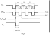
- Fig. 8 is an operation timing diagram of a driving apparatus in a display apparatus according to an embodiment of the present disclosure.
- a high level voltage ELVH and a low level voltage ELVL are provided to the display apparatus, and a voltage selector is provided to the display apparatus. That is, the level control signal is a power supply signal of the light-emitting element.
- the voltage selector receives a dual-level signal, i.e., a high level power supply signal and a low level power supply signal.
- the source driving circuit 600 outputs a selection signal EL C to the voltage selector, to cause the voltage selector to selectively output one of the high level power supply signal and the low level power supply signal.
- the driving control circuit provides the driving voltage to the driving element according to the data signal and the parameter of the driving element to drive the light-emitting element to emit light by the driving element, and when the level control signal is the low level power supply signal, the provided driving voltage is unable to drive the driving element and thereby the light-emitting element does not emit light.
- the selection signal EL C outputted by the source driving circuit is a pulse control signal having a duty ratio of D.
- This pulse has the same period as a period of the row scanning signal of the display apparatus, and is divided into a high level and a low level within the period of the row scanning signal, so that the voltage ELV DD of the power supply signal output by the voltage selector is also correspondingly divided into a high level and a low level, which represent a light emission sub-phase and a non-light emission sub-phase of the light-emitting element, respectively.
- the data signal cannot be written when the voltage of the power supply signal is at a low level since the signal written at this time is no longer a data voltage corresponding to the data signal.
- the row scanning signal Gm is correspondingly adjusted so that a gating time thereof is the same as duration of the high level power supply signal. That is, the level control signal is synchronous with the row scanning signal.
- the duty ratio between the high level and the low level of EL C may be correspondingly adjusted to achieve a desired driving current density. However, a minimum duty ratio of EL C needs to ensure a data write time.
- the voltage selector is provided outside the source driving circuit. According to another embodiment, the voltage selector may be included in the source driving circuit.
- the voltage selector comprises a high level voltage power supply for outputting a high level power supply signal and a low level voltage power supply for outputting a low level power supply signal.
- the selection signal EL C is generated by the source driving circuit or an external circuit.
- Fig. 9 illustrates a diagram of a voltage selector according to an embodiment of the present disclosure.
- the voltage selector 900 comprises a first transistor T1 having a gate configured to receive a selection signal of the driving voltage control circuit, a source configured to receive the high level power supply signal, and a drain connected to a gate of a second transistor T2; the second transistor T2 having a source configured to receive the high level power supply signal, and a drain connected to an output terminal; a first resistor R1 having one end connected to the gate of the second transistor T2 and the other end connected to the ground; a third transistor T3 having a gate connected to a source of a fourth transistor T4, a source configured to receive the low level power supply signal, and a drain connected to the output end; the fourth transistor T4 having a gate configured to receive the selection signal of the driving voltage control circuit and a drain connected to the ground; and a second resistor R2 having one end connected to the source of the third transistor T3 and the other end connected to the ground; and a second
- the selection signal EL C selects the high level signal EL VDDH , the transistors T1 and T4 are turned on, T3 is turned off, and T2 is turned on. Therefore, the voltage EL VDD of the output power supply signal is equal to EL VDDH minus a turn-on voltage of T1, and as a result, the output voltage is a power supply signal which is approximately equal to EL VDDH .
- the selection signal EL C selects the low level signal EL VDDL , T1 and T4 are turned off, T2 is turned off, and T3 is turned on.
- the voltage EL VDD of the output power supply signal is equal to EL VDDL minus a turn-on voltage of T3, and as a result, the output voltage is a power supply signal which is approximately equal to EL VDDL . Therefore, the high level power supply signal and low level power supply signal can be selectively output by controlling the selection signal EL C .
- PMOS transistors will be described as an example.
- NMOS transistors or other transistors, or even other connection manners may be used as well, as long as the high level signal EL VDDH and the low level signal EL VDDL are input, and the output power supply signal selectively outputs a high level power supply signal and a low level power supply signal according to the selection signal.
- the voltage selector may also be integrated into the source driving circuit.
- Fig. 10 illustrates a structural diagram of a display apparatus according to another embodiment of the present disclosure.
- the source driving circuit receives a high level power supply signal and a low level power supply signal, selectively outputs one of the high level power supply signal and the low level power supply signal to the driving element during scanning of each row, wherein the high level power supply signal drives the light-emitting element to emit light, and the low level power supply signal cannot drive the light-emitting element to emit light.
- the density of the driving current can be adjusted by adjusting the driving voltage provided in the light emission phase of the light-emitting element, thereby improving the display quality.
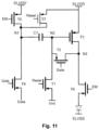
- Fig. 11 illustrates a structural diagram of a display apparatus of an 8.4-inch flat panel.
- Fig. 12 illustrates an operation timing diagram of a driving apparatus in the display apparatus shown in Fig. 11 .
- an operation timing of the display apparatus shown in Fig. 11 is as follows:
- ELV DD is a single-level signal.
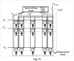
- Fig. 13 is a structural diagram of a display apparatus according to an embodiment of the present disclosure.
- the driving apparatus of the display apparatus according to the embodiment of the present disclosure further comprises a reference voltage control circuit configured to generate a high level reference voltage and a low level reference voltage.
- the reference voltage control circuit of the driving apparatus is configured to generate a high level reference voltage and a low level reference voltage.
- the driving control circuit is configured to provide a high/low level signal to a control terminal of the driving element according to the reference voltage.
- a signal at one of the high level and the low level causes the driving element to be driven normally; and a signal at the other of the high level and the low level causes the driving element to be in a cut-off state or in a slight turn-on state.
- the high level reference voltage and the low level reference voltage are generated by the reference voltage control circuit.
- voltage amplitude may be adjusted through programming.
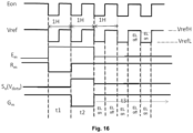
- Fig. 14 is an operation timing diagram of a driving apparatus in a display apparatus according to an embodiment of the present disclosure.
- an operation timing of the driving apparatus in the display apparatus shown in Fig. 13 is as follows:
- the emission luminance of the light-emitting element that is, the current density of the light-emitting element
- the emission luminance of the light-emitting element can be adjusted by adjusting a duty ratio between VrefL and VrefH.
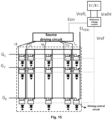
- Fig. 15 illustrates a structural diagram of a display apparatus according to another embodiment of the present disclosure.
- a high level reference voltage and a low level reference voltage are generated by an external circuit.
- the driving apparatus comprises a source driving circuit, a driving control circuit, a driving element, and a light-emitting element.
- the source driving circuit outputs a selection signal to a reference voltage control circuit which receives the high level reference voltage and the low level reference voltage, to cause the reference voltage control circuit to selectively output one of the high level reference voltage and the low level reference voltage, so that the driving control circuit provides a high level driving voltage and a low level driving voltage.
- Fig. 16 illustrates an operation timing diagram of a driving apparatus in the display apparatus shown in Fig. 15 .
- the reference voltage selection circuit selectively outputs VrefH or VrefL according to a selection signal E on output by the source driving circuit.
- the driving apparatus is shown in Fig. 6
- the display apparatuses are shown in Figs. 7 , 10 , 13 , and 15
- the voltage selector is shown in Fig. 9
- these circuits and apparatuses may use other structures.
- the driving apparatus according to the embodiment of the present disclosure may be applied to a display apparatus having another structure
- the voltage selector according to the embodiment of the present disclosure may be applied to a driving apparatus having another structure.
- These figures are shown by way of example only.
- the structure of the voltage selector shown in Fig. 9 may not be limited to the illustrated structure.
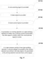
- Fig. 17 illustrates a flowchart of a driving method for a driving apparatus according to an embodiment of the present disclosure.
- the driving method for the driving apparatus comprises the following steps.
- step S1710 a row scanning signal is provided on a row scanning line.
- step S1720 a data signal is provided on a data line.
- step S1730 a level control signal is provided.
- step S1740 a parameter of a driving element for a light-emitting element is written into a driving control circuit while writing the data signal when the row scanning signal is valid.
- step S1750 in a light emission phase of the light-emitting element, a driving voltage is provided to the driving element according to the data signal, the parameter of the driving element and the level control signal; wherein the level control signal is configured to comprise a high level and a low level, one of which causes the driving voltage not to be sufficient enough to drive the driving element, and the other of which causes the driving voltage to be provided to the driving element according to the data signal and the parameter of the driving element to cause the light-emitting element to emit light.
- Steps S1710-S1730 may be performed in parallel.
- the row scanning line is connected to a row scanning signal source
- the data line is connected to a data source
- a source of the level control signal is connected to a line of the level control signal in advance.
- steps S1710-S1730 are performed so that the display apparatus enters a data write phase, i.e., the row scanning signal is valid while writing the data signal.
- the parameter of the driving element for the light-emitting element is written into the driving control circuit.
- step S1750 the driving voltage is provided to the driving element according to the data signal, the parameter of the driving element, and the level control signal which have been written.
- the level control signal may be a power supply signal of the light-emitting element. That is, when the level control signal is at a high level, the driving control circuit provides the driving voltage to the driving element according to the data signal and the parameter of the driving element to drive the light-emitting element to emit light by the driving element; and when the level control signal is at a low level, the provided driving voltage is unable to drive the driving element and thereby the light-emitting element does not emit light.
- the level control signal may be applied to a control terminal of the driving element.
- the level control signal at one of a high level and a low level causes the driving element to be driven normally, and the level control signal at the other of the high level and the low level causes the driving element to be in a cut-off state or in a slight turn-on state.
- the level control signal is synchronous with the row scanning signal. That is, a gating time of the row scanning signal is the same as duration of the high level power supply signal so that the data signal is not written when the power supply signal is at a low level.
Landscapes
- Engineering & Computer Science (AREA)
- Physics & Mathematics (AREA)
- Computer Hardware Design (AREA)
- General Physics & Mathematics (AREA)
- Theoretical Computer Science (AREA)
- Control Of Indicators Other Than Cathode Ray Tubes (AREA)
- Control Of El Displays (AREA)
- Electroluminescent Light Sources (AREA)
Claims (13)
- Ansteuerungseinrichtung zum Ansteuern eines lichtemittierenden Elements, umfassend:eine Quellenansteuerungsschaltung, ausgelegt zum Erzeugen eines Zeilenabtastsignals, das zum Ansteuern des lichtemittierenden Elements erforderlich ist, und eines Datensignals, wobei das Datensignal in eine Ansteuerungssteuerschaltung für das lichtemittierende Element geschrieben wird, wenn das Zeilenabtastsignal gültig ist;wobei die Ansteuerungssteuerschaltung ausgelegt ist zum Schreiben eines Parameters eines Ansteuerungselements für das lichtemittierende Element während des Schreibens des Datensignals, wenn das Zeilenabtastsignal gültig ist, wobei die Ansteuerungssteuerschaltung ferner ausgelegt ist zum Empfangen eines Pegelsteuersignals und Liefern einer Ansteuerungsspannung an das Ansteuerungselement gemäß dem Datensignal, dem Parameter des Ansteuerungselements und dem Pegelsteuersignal in einer Lichtemissionsphase des lichtemittierenden Elements; und wobei das Ansteuerungselement ausgelegt ist zum Umwandeln der durch die Ansteuerungssteuerschaltung gelieferten Ansteuerungsspannung in einen Ansteuerungsstrom und Liefern des Ansteuerungsstroms an das lichtemittierende Element, sodass das lichtemittierende Element unter der Ansteuerung des durch das Ansteuerungselement gelieferten Ansteuerungsstroms Licht emittiert;wobei das Pegelsteuersignal ein Leistungsversorgungssignal des lichtemittierenden Elements ist und dazu ausgelegt ist, einen hohen Pegel und einen niedrigen Pegel zu umfassen, wobei, wenn das Pegelsteuersignal auf einem niedrigen Pegel ist, die gelieferte Ansteuerungsspannung nicht ausreicht, um das Ansteuerungselement anzusteuern, und wenn das Pegelsteuersignal auf einem hohen Pegel ist, die Ansteuerungssteuerschaltung die Ansteuerungsspannung gemäß dem Datensignal und dem Parameter des Ansteuerungselements an das Ansteuerungselement liefert, um zu bewirken, dass das lichtemittierende Element Licht emittiert;wobei die Ansteuerungseinrichtung ferner einen Spannungsselektor umfasst, der eine Spannungsleistungsversorgung mit hohem Pegel zum Ausgeben eines Leistungsversorgungssignals mit hohem Pegel und eine Spannungsleistungsversorgung mit niedrigem Pegel zum Ausgeben eines Leistungsversorgungssignals mit niedrigen Pegel aufweist und der Spannungsselektor ein Auswahlsignal empfängt und eine Ausgabe eines Leistungsversorgungssignals auf einem hohen Pegel oder einem niedrigen Pegel gemäß dem Auswahlsignal auswählt;dadurch gekennzeichnet, dassder Spannungsselektor Folgendes umfasst:einen ersten Transistor mit einem Gate, das zum Empfangen des Auswahlsignals der Ansteuerungsspannungssteuerschaltung ausgelegt ist,einer ersten Elektrode, die zum Empfangen eines Leistungsversorgungsignals mit hohem Pegel ausgelegt ist, und einer zweiten Elektrode, die mit einem Gate eines zweiten Transistors verbunden ist;den zweiten Transistor mit einer ersten Elektrode, die zum Empfangen des Leistungsversorgungsignals mit hohem Pegel ausgelegt ist, und einer zweiten Elektrode, die mit einem Ausgangsanschluss verbunden ist;einen ersten Widerstand, bei dem ein Ende mit dem Gate des zweiten Transistors verbunden ist und das andere Ende mit Masse verbunden ist;einen dritten Transistor mit einem Gate, das mit einer ersten Elektrode eines vierten Transistors verbunden ist, einer ersten Elektrode, die zum Empfangen eines Leistungsversorgungssignals mit niedrigem Pegel ausgelegt ist, und einer zweiten Elektrode, die mit dem Ausgangsende verbunden ist;den vierten Transistor mit einem Gate, das zum Empfangen des Auswahlsignals der Ansteuerungsspannungssteuerschaltung ausgelegt ist, und einer zweiten Elektrode, die mit Masse verbunden ist; und einen zweiten Widerstand, bei dem ein Ende mit der Source des dritten Transistors verbunden ist und das andere Ende mit dem Gate des dritten Transistors verbunden ist.
- Ansteuerungseinrichtung nach Anspruch 1, wobei eines des Leistungsversorgungssignals mit hohem Pegel und des Leistungsversorgungssignals mit niedrigem Pegel als Leistungsversorgungssignal zum Bewirken, dass das lichtemittierende Element Licht normal emittiert, eingestellt ist, und wenn das andere des Leistungsversorgungssignals mit hohem Pegel und das Leistungsversorgungsignal mit niedrigem Pegel als Leistungsversorgungsignal eingestellt ist und das Leistungsversorgungsignal angelegt wird, Ansteuerungselemente unter allen Datensignalen alle in einem Sperrzustand sind.
- Ansteuerungseinrichtung nach Anspruch 1, wobei das Auswahlsignal durch die Quellenansteuerungsschaltung oder eine externe Schaltung erzeugt wird.
- Ansteuerungseinrichtung nach Anspruch 1, wobei der Spannungsselektor in der Quellenansteuerungsschaltung enthalten ist.
- Ansteuerungseinrichtung nach Anspruch 1, wobei das Pegelsteuersignal in einen Steueranschluss des Ansteuerungselement eingegeben wird, wobei das Pegelsteuersignal auf einem des hohen Pegels und des niedrigen Pegels bewirkt, dass das Ansteuerungselement normal angesteuert wird, und das Pegelsteuersignal auf dem anderen des hohen Pegels und des niedrigen Pegels bewirkt, dass sich das Ansteuerungselement in einem Sperrzustand oder in einem schwachen Einschaltzustand befindet.
- Ansteuerungseinrichtung nach Anspruch 5, wobei das Pegelsteuersignal durch die Quellenansteuerungsschaltung oder eine externe Schaltung erzeugt wird.
- Ansteuerungseinrichtung nach an einem der Ansprüche 1-6, wobei das Pegelsteuersignal synchron zu dem Zeilenabtastsignal ist.
- Ansteuerungseinrichtung nach einem der Ansprüche 1-6, wobei ein Tastverhältnis zwischen dem hohen Pegel und dem niedrigen Pegel des Pegelsteuersignals einstellbar ist.
- Verfahren zum Ansteuern eines lichtemittierenden Elements, das in der Ansteuerungseinrichtung nach Anspruch 1 angewendet wird, umfassend:Liefern eines Zeilenabtastsignals auf einer Zeilenabtastleitung;Liefern eines Datensignals auf einer Datenleitung;Liefern eines Pegelsteuersignals;Schreiben eines Parameters eines Ansteuerungselements des lichtemittierenden Elements in eine Ansteuerungssteuerschaltung während des Schreibens des Datensignals, wenn das Zeilenabtastsignal gültig ist; undLiefern einer Ansteuerungsspannung an das Ansteuerungselement gemäß dem Datensignal, dem Parameter des Ansteuerungselements und dem Pegelsteuersignal in einer Lichtemissionsphase des lichtemittierenden Elements;wobei das Pegelsteuersignal dazu ausgelegt ist, einen hohen Pegel und einen niedrigen Pegel zu umfassen, von denen einer bewirkt, dass die Ansteuerungsspannung nicht ausreicht, um das Ansteuerungselement anzusteuern, und der andere bewirkt, dass die Ansteuerungssteuerschaltung die Ansteuerungsspannung gemäß dem Datensignal und dem Parameter des Ansteuerungselements an das Ansteuerungselement geliefert wird, um zu bewirken, dass das lichtemittierende Element Licht emittiert.
- Verfahren nach Anspruch 9, wobei
das Pegelsteuersignal ein Leistungsversorgungssignal des lichtemittierenden Elements ist. - Verfahren nach Anspruch 9, wobeidas Pegelsteuersignal an einen Steueranschluss des Ansteuerungselement angelegt wird,wobei das Pegelsteuersignal auf einem des hohen Pegels und des niedrigen Pegels bewirkt, dass das Ansteuerungselement normal angesteuert wird, und das Pegelsteuersignal auf dem anderen des hohen Pegels und des niedrigen Pegels bewirkt, dass sich das Ansteuerungselement in einem Sperrzustand oder in einem schwachen Einschaltzustand befindet.
- Verfahren nach einem der Ansprüche 9-11, wobei das Pegelsteuersignal synchron zu den Zeilenabtastsignal ist.
- Anzeigeeinrichtung, umfassend:die Ansteuerungseinrichtung nach einem der Ansprüche 1-8; undlichtemittierende Elemente, die jeweils dazu ausgelegt sind, Licht gemäß dem durch die Ansteuerungseinrichtung gelieferten Ansteuerungsstrom zu emittieren.
Priority Applications (1)
| Application Number | Priority Date | Filing Date | Title |
|---|---|---|---|
| EP23158393.1A EP4213140A1 (de) | 2015-12-31 | 2016-07-04 | Ansteuerungsvorrichtung, ansteuerungsverfahren und anzeigevorrichtung |
Applications Claiming Priority (2)
| Application Number | Priority Date | Filing Date | Title |
|---|---|---|---|
| CN201511021518.4A CN105609053B (zh) | 2015-12-31 | 2015-12-31 | 驱动装置、驱动方法和显示装置 |
| PCT/CN2016/088370 WO2017113678A1 (zh) | 2015-12-31 | 2016-07-04 | 一种驱动装置、驱动方法和显示装置 |
Related Child Applications (2)
| Application Number | Title | Priority Date | Filing Date |
|---|---|---|---|
| EP23158393.1A Division EP4213140A1 (de) | 2015-12-31 | 2016-07-04 | Ansteuerungsvorrichtung, ansteuerungsverfahren und anzeigevorrichtung |
| EP23158393.1A Division-Into EP4213140A1 (de) | 2015-12-31 | 2016-07-04 | Ansteuerungsvorrichtung, ansteuerungsverfahren und anzeigevorrichtung |
Publications (3)
| Publication Number | Publication Date |
|---|---|
| EP3208794A1 EP3208794A1 (de) | 2017-08-23 |
| EP3208794A4 EP3208794A4 (de) | 2018-05-16 |
| EP3208794B1 true EP3208794B1 (de) | 2023-05-03 |
Family
ID=55988944
Family Applications (2)
| Application Number | Title | Priority Date | Filing Date |
|---|---|---|---|
| EP16831883.0A Active EP3208794B1 (de) | 2015-12-31 | 2016-07-04 | Treibervorrichtung, fahrmethode und displayvorrichtung |
| EP23158393.1A Pending EP4213140A1 (de) | 2015-12-31 | 2016-07-04 | Ansteuerungsvorrichtung, ansteuerungsverfahren und anzeigevorrichtung |
Family Applications After (1)
| Application Number | Title | Priority Date | Filing Date |
|---|---|---|---|
| EP23158393.1A Pending EP4213140A1 (de) | 2015-12-31 | 2016-07-04 | Ansteuerungsvorrichtung, ansteuerungsverfahren und anzeigevorrichtung |
Country Status (4)
| Country | Link |
|---|---|
| US (1) | US10319295B2 (de) |
| EP (2) | EP3208794B1 (de) |
| CN (1) | CN105609053B (de) |
| WO (1) | WO2017113678A1 (de) |
Families Citing this family (8)
| Publication number | Priority date | Publication date | Assignee | Title |
|---|---|---|---|---|
| CN105609053B (zh) | 2015-12-31 | 2019-01-22 | 京东方科技集团股份有限公司 | 驱动装置、驱动方法和显示装置 |
| CN108122534B (zh) | 2016-11-29 | 2019-03-26 | 昆山国显光电有限公司 | 一种驱动控制电路及其驱动方法、显示装置 |
| CN107516490A (zh) * | 2017-09-14 | 2017-12-26 | 北京大学深圳研究生院 | 像素装置、用于像素装置的驱动方法和显示设备 |
| KR102395792B1 (ko) | 2017-10-18 | 2022-05-11 | 삼성디스플레이 주식회사 | 표시 장치 및 그 구동 방법 |
| CN109935213B (zh) * | 2017-12-15 | 2021-03-30 | 京东方科技集团股份有限公司 | 显示面板的亮度调节方法、显示面板及其驱动方法 |
| CN109658874B (zh) * | 2019-01-24 | 2020-12-25 | 苏州奥素液芯电子科技有限公司 | 一种驱动装置及驱动方法、电润湿系统 |
| CN113674677B (zh) * | 2021-08-09 | 2023-12-19 | Tcl华星光电技术有限公司 | 显示面板及显示装置 |
| CN113744683B (zh) * | 2021-09-03 | 2023-06-27 | 北京京东方技术开发有限公司 | 像素电路、驱动方法和显示装置 |
Family Cites Families (43)
| Publication number | Priority date | Publication date | Assignee | Title |
|---|---|---|---|---|
| JP4023335B2 (ja) * | 2003-02-19 | 2007-12-19 | セイコーエプソン株式会社 | 電気光学装置、電気光学装置の駆動方法および電子機器 |
| KR100560780B1 (ko) * | 2003-07-07 | 2006-03-13 | 삼성에스디아이 주식회사 | 유기전계 발광표시장치의 화소회로 및 그의 구동방법 |
| KR100673760B1 (ko) * | 2004-09-08 | 2007-01-24 | 삼성에스디아이 주식회사 | 발광 표시장치 |
| KR101018751B1 (ko) * | 2004-09-24 | 2011-03-04 | 삼성전자주식회사 | 표시 장치 및 그 구동 방법 |
| KR100604057B1 (ko) * | 2004-09-24 | 2006-07-24 | 삼성에스디아이 주식회사 | 화소 및 이를 이용한 발광 표시장치 |
| KR100635509B1 (ko) * | 2005-08-16 | 2006-10-17 | 삼성에스디아이 주식회사 | 유기 전계발광 표시장치 |
| CN101273398B (zh) * | 2005-09-27 | 2011-06-01 | 卡西欧计算机株式会社 | 显示装置及显示装置的驱动方法 |
| JP5082319B2 (ja) * | 2006-07-25 | 2012-11-28 | ソニー株式会社 | 発光条件制御装置、画像処理装置、自発光表示装置、電子機器、発光条件制御方法及びコンピュータプログラム |
| CN100514424C (zh) | 2006-09-08 | 2009-07-15 | 胜华科技股份有限公司 | 有机电激发光二极体的驱动电路及其驱动方法 |
| KR100876250B1 (ko) * | 2007-01-15 | 2008-12-26 | 삼성모바일디스플레이주식회사 | 유기 전계 발광 표시 장치 |
| KR100865394B1 (ko) * | 2007-03-02 | 2008-10-24 | 삼성에스디아이 주식회사 | 유기 전계 발광 표시 장치 |
| KR100873078B1 (ko) * | 2007-04-10 | 2008-12-09 | 삼성모바일디스플레이주식회사 | 화소 및 이를 이용한 유기전계발광 표시장치 및 그의구동방법 |
| JP4715849B2 (ja) | 2008-01-15 | 2011-07-06 | ソニー株式会社 | 表示装置及びその駆動方法と電子機器 |
| KR20100009219A (ko) * | 2008-07-18 | 2010-01-27 | 삼성모바일디스플레이주식회사 | 화소 및 이를 이용한 유기전계발광 표시장치 |
| JP2010048985A (ja) * | 2008-08-21 | 2010-03-04 | Sony Corp | 半導体集積回路、自発光表示パネルモジュール、電子機器及び電源線駆動方法 |
| JP2010107630A (ja) * | 2008-10-29 | 2010-05-13 | Sony Corp | 画像表示装置及び画像表示装置の駆動方法 |
| JP5580536B2 (ja) * | 2009-01-09 | 2014-08-27 | グローバル・オーエルイーディー・テクノロジー・リミテッド・ライアビリティ・カンパニー | 表示装置 |
| KR101058110B1 (ko) * | 2009-09-16 | 2011-08-24 | 삼성모바일디스플레이주식회사 | 디스플레이 패널의 화소 회로, 그 구동방법, 및 이를 포함하는 유기 발광 표시 장치 |
| KR101058111B1 (ko) * | 2009-09-22 | 2011-08-24 | 삼성모바일디스플레이주식회사 | 디스플레이 패널의 화소 회로, 그 구동방법, 및 이를 포함하는 유기 발광 표시 장치 |
| KR101030002B1 (ko) * | 2009-10-08 | 2011-04-20 | 삼성모바일디스플레이주식회사 | 화소 회로 및 이를 이용한 유기전계발광 표시 장치 |
| KR101056223B1 (ko) * | 2009-11-06 | 2011-08-11 | 삼성모바일디스플레이주식회사 | 화소 및 이를 이용한 유기전계발광 표시장치 |
| KR101113430B1 (ko) * | 2009-12-10 | 2012-03-02 | 삼성모바일디스플레이주식회사 | 화소 및 그를 이용한 유기전계발광표시장치 |
| KR101049809B1 (ko) * | 2010-01-21 | 2011-07-15 | 삼성모바일디스플레이주식회사 | 표시 장치 및 그 구동 방법 |
| KR20110121889A (ko) * | 2010-05-03 | 2011-11-09 | 삼성모바일디스플레이주식회사 | 화소 및 그를 이용한 유기전계발광표시장치 |
| KR101329967B1 (ko) * | 2010-05-11 | 2013-11-13 | 엘지디스플레이 주식회사 | 백 라이트 유닛과 이를 이용한 액정 표시장치 및 그의 구동방법 |
| KR101082234B1 (ko) * | 2010-05-13 | 2011-11-09 | 삼성모바일디스플레이주식회사 | 유기전계발광 표시장치 및 그의 구동방법 |
| KR101152580B1 (ko) * | 2010-06-30 | 2012-06-01 | 삼성모바일디스플레이주식회사 | 화소 및 이를 이용한 유기전계발광 표시장치 |
| KR101682690B1 (ko) * | 2010-07-20 | 2016-12-07 | 삼성디스플레이 주식회사 | 화소 및 이를 이용한 유기전계발광 표시장치 |
| KR101692367B1 (ko) * | 2010-07-22 | 2017-01-04 | 삼성디스플레이 주식회사 | 화소 및 이를 이용한 유기전계발광 표시장치 |
| KR101760090B1 (ko) * | 2010-08-11 | 2017-07-21 | 삼성디스플레이 주식회사 | 화소 및 이를 이용한 유기전계발광 표시장치 |
| KR20120065716A (ko) * | 2010-12-13 | 2012-06-21 | 삼성모바일디스플레이주식회사 | 표시 장치 및 그 구동 방법 |
| KR20120074847A (ko) * | 2010-12-28 | 2012-07-06 | 삼성모바일디스플레이주식회사 | 화소 및 이를 이용한 유기 발광 표시 장치 |
| KR101399159B1 (ko) * | 2011-12-01 | 2014-05-28 | 엘지디스플레이 주식회사 | 유기발광 표시장치 |
| TWI471843B (zh) | 2012-07-18 | 2015-02-01 | Innocom Tech Shenzhen Co Ltd | 有機發光二極體像素電路與顯示器 |
| KR20140013587A (ko) * | 2012-07-25 | 2014-02-05 | 삼성디스플레이 주식회사 | 화소 및 이를 이용한 유기전계발광 표시장치 |
| JP6082908B2 (ja) * | 2012-11-13 | 2017-02-22 | 株式会社Joled | 表示装置および表示装置の駆動方法 |
| KR101980777B1 (ko) | 2013-03-25 | 2019-05-21 | 엘지디스플레이 주식회사 | Oled 표시 장치 및 그의 구동 방법 |
| KR102083458B1 (ko) * | 2013-12-26 | 2020-03-02 | 엘지디스플레이 주식회사 | 유기발광 표시장치 |
| JP6561413B2 (ja) * | 2014-04-28 | 2019-08-21 | 株式会社Joled | 表示装置、駆動方法、および電子機器 |
| CN104882094A (zh) * | 2015-04-30 | 2015-09-02 | 武汉精测电子技术股份有限公司 | 一种oled面板驱动电路、驱动方法及显示装置 |
| CN105139804B (zh) | 2015-09-28 | 2018-12-21 | 京东方科技集团股份有限公司 | 一种像素驱动电路、显示面板及其驱动方法和显示装置 |
| CN205282059U (zh) * | 2015-12-31 | 2016-06-01 | 京东方科技集团股份有限公司 | 驱动装置和显示装置 |
| CN105609053B (zh) | 2015-12-31 | 2019-01-22 | 京东方科技集团股份有限公司 | 驱动装置、驱动方法和显示装置 |
-
2015
- 2015-12-31 CN CN201511021518.4A patent/CN105609053B/zh active Active
-
2016
- 2016-07-04 EP EP16831883.0A patent/EP3208794B1/de active Active
- 2016-07-04 EP EP23158393.1A patent/EP4213140A1/de active Pending
- 2016-07-04 US US15/502,274 patent/US10319295B2/en active Active
- 2016-07-04 WO PCT/CN2016/088370 patent/WO2017113678A1/zh not_active Ceased
Also Published As
| Publication number | Publication date |
|---|---|
| EP4213140A1 (de) | 2023-07-19 |
| US10319295B2 (en) | 2019-06-11 |
| EP3208794A1 (de) | 2017-08-23 |
| CN105609053B (zh) | 2019-01-22 |
| WO2017113678A1 (zh) | 2017-07-06 |
| EP3208794A4 (de) | 2018-05-16 |
| US20180068616A1 (en) | 2018-03-08 |
| CN105609053A (zh) | 2016-05-25 |
Similar Documents
| Publication | Publication Date | Title |
|---|---|---|
| EP3208794B1 (de) | Treibervorrichtung, fahrmethode und displayvorrichtung | |
| US10861393B2 (en) | Organic light emitting display device | |
| US11551606B2 (en) | LED driving circuit, display panel, and pixel driving device | |
| JP5560206B2 (ja) | 有機el表示装置及びその制御方法 | |
| EP1496495B1 (de) | Pixelschaltung für eine organische lichtemittierende Vorrichtung mit Selbstkompensation der Schwellenspannung und Ansteuerungsverfahren dafür | |
| US7015882B2 (en) | Active matrix display and active matrix organic electroluminescence display | |
| KR101596977B1 (ko) | 유기 el 표시 장치 및 그 제어 방법 | |
| JP4398413B2 (ja) | スレッショルド電圧の補償を備えた画素駆動回路 | |
| JP5266667B2 (ja) | 画素およびディスプレイパネル | |
| US10504440B2 (en) | Pixel circuit, driving method thereof, display panel and display apparatus | |
| US9905166B2 (en) | Pixel driving circuit, pixel driving method and display apparatus | |
| KR102715269B1 (ko) | 게이트 드라이버, 유기발광표시장치 및 그의 구동방법 | |
| US20110057864A1 (en) | Emission control driver and organic light emitting display using the same | |
| JP2004110015A (ja) | 表示装置及びその駆動方法 | |
| KR20200036415A (ko) | 표시 장치 | |
| JP2005165320A (ja) | 発光表示装置及びその駆動方法 | |
| US8059072B2 (en) | Pixels, display devices utilizing same, and pixel driving methods | |
| CN205282059U (zh) | 驱动装置和显示装置 | |
| US12118936B2 (en) | Pixel circuit and driving method thereof and display panel having the same | |
| JP6379344B2 (ja) | 表示装置の駆動方法 | |
| JP5789585B2 (ja) | 表示装置および電子機器 | |
| KR101338903B1 (ko) | 표시패널, 이를 갖는 표시장치 및 이의 구동방법 | |
| JP2010008941A (ja) | 画素回路及び表示装置 | |
| KR100595108B1 (ko) | 화소와 발광 표시장치 및 그의 구동방법 | |
| US20140320471A1 (en) | Driving method and pixel unit of active matrix organic light-emitting diode panel |
Legal Events
| Date | Code | Title | Description |
|---|---|---|---|
| STAA | Information on the status of an ep patent application or granted ep patent |
Free format text: STATUS: UNKNOWN |
|
| STAA | Information on the status of an ep patent application or granted ep patent |
Free format text: STATUS: THE INTERNATIONAL PUBLICATION HAS BEEN MADE |
|
| PUAI | Public reference made under article 153(3) epc to a published international application that has entered the european phase |
Free format text: ORIGINAL CODE: 0009012 |
|
| STAA | Information on the status of an ep patent application or granted ep patent |
Free format text: STATUS: REQUEST FOR EXAMINATION WAS MADE |
|
| 17P | Request for examination filed |
Effective date: 20170210 |
|
| AK | Designated contracting states |
Kind code of ref document: A1 Designated state(s): AL AT BE BG CH CY CZ DE DK EE ES FI FR GB GR HR HU IE IS IT LI LT LU LV MC MK MT NL NO PL PT RO RS SE SI SK SM TR |
|
| AX | Request for extension of the european patent |
Extension state: BA ME |
|
| RIC1 | Information provided on ipc code assigned before grant |
Ipc: G09G 3/3258 20160101AFI20170811BHEP |
|
| RIN1 | Information on inventor provided before grant (corrected) |
Inventor name: YIN, XINSHE |
|
| R17P | Request for examination filed (corrected) |
Effective date: 20170210 |
|
| A4 | Supplementary search report drawn up and despatched |
Effective date: 20180417 |
|
| RIC1 | Information provided on ipc code assigned before grant |
Ipc: G09G 3/3291 20160101ALI20180411BHEP Ipc: G09G 3/3258 20160101AFI20180411BHEP Ipc: G09G 3/20 20060101ALI20180411BHEP |
|
| DAV | Request for validation of the european patent (deleted) | ||
| DAX | Request for extension of the european patent (deleted) | ||
| STAA | Information on the status of an ep patent application or granted ep patent |
Free format text: STATUS: EXAMINATION IS IN PROGRESS |
|
| 17Q | First examination report despatched |
Effective date: 20190709 |
|
| GRAP | Despatch of communication of intention to grant a patent |
Free format text: ORIGINAL CODE: EPIDOSNIGR1 |
|
| STAA | Information on the status of an ep patent application or granted ep patent |
Free format text: STATUS: GRANT OF PATENT IS INTENDED |
|
| INTG | Intention to grant announced |
Effective date: 20221205 |
|
| GRAS | Grant fee paid |
Free format text: ORIGINAL CODE: EPIDOSNIGR3 |
|
| GRAA | (expected) grant |
Free format text: ORIGINAL CODE: 0009210 |
|
| STAA | Information on the status of an ep patent application or granted ep patent |
Free format text: STATUS: THE PATENT HAS BEEN GRANTED |
|
| AK | Designated contracting states |
Kind code of ref document: B1 Designated state(s): AL AT BE BG CH CY CZ DE DK EE ES FI FR GB GR HR HU IE IS IT LI LT LU LV MC MK MT NL NO PL PT RO RS SE SI SK SM TR |
|
| REG | Reference to a national code |
Ref country code: GB Ref legal event code: FG4D |
|
| REG | Reference to a national code |
Ref country code: DE Ref legal event code: R096 Ref document number: 602016079220 Country of ref document: DE |
|
| REG | Reference to a national code |
Ref country code: AT Ref legal event code: REF Ref document number: 1565342 Country of ref document: AT Kind code of ref document: T Effective date: 20230515 Ref country code: CH Ref legal event code: EP |
|
| REG | Reference to a national code |
Ref country code: IE Ref legal event code: FG4D |
|
| REG | Reference to a national code |
Ref country code: LT Ref legal event code: MG9D |
|
| REG | Reference to a national code |
Ref country code: NL Ref legal event code: MP Effective date: 20230503 |
|
| REG | Reference to a national code |
Ref country code: AT Ref legal event code: MK05 Ref document number: 1565342 Country of ref document: AT Kind code of ref document: T Effective date: 20230503 |
|
| PG25 | Lapsed in a contracting state [announced via postgrant information from national office to epo] |
Ref country code: SE Free format text: LAPSE BECAUSE OF FAILURE TO SUBMIT A TRANSLATION OF THE DESCRIPTION OR TO PAY THE FEE WITHIN THE PRESCRIBED TIME-LIMIT Effective date: 20230503 Ref country code: PT Free format text: LAPSE BECAUSE OF FAILURE TO SUBMIT A TRANSLATION OF THE DESCRIPTION OR TO PAY THE FEE WITHIN THE PRESCRIBED TIME-LIMIT Effective date: 20230904 Ref country code: NO Free format text: LAPSE BECAUSE OF FAILURE TO SUBMIT A TRANSLATION OF THE DESCRIPTION OR TO PAY THE FEE WITHIN THE PRESCRIBED TIME-LIMIT Effective date: 20230803 Ref country code: NL Free format text: LAPSE BECAUSE OF FAILURE TO SUBMIT A TRANSLATION OF THE DESCRIPTION OR TO PAY THE FEE WITHIN THE PRESCRIBED TIME-LIMIT Effective date: 20230503 Ref country code: ES Free format text: LAPSE BECAUSE OF FAILURE TO SUBMIT A TRANSLATION OF THE DESCRIPTION OR TO PAY THE FEE WITHIN THE PRESCRIBED TIME-LIMIT Effective date: 20230503 Ref country code: AT Free format text: LAPSE BECAUSE OF FAILURE TO SUBMIT A TRANSLATION OF THE DESCRIPTION OR TO PAY THE FEE WITHIN THE PRESCRIBED TIME-LIMIT Effective date: 20230503 |
|
| PG25 | Lapsed in a contracting state [announced via postgrant information from national office to epo] |
Ref country code: RS Free format text: LAPSE BECAUSE OF FAILURE TO SUBMIT A TRANSLATION OF THE DESCRIPTION OR TO PAY THE FEE WITHIN THE PRESCRIBED TIME-LIMIT Effective date: 20230503 Ref country code: PL Free format text: LAPSE BECAUSE OF FAILURE TO SUBMIT A TRANSLATION OF THE DESCRIPTION OR TO PAY THE FEE WITHIN THE PRESCRIBED TIME-LIMIT Effective date: 20230503 Ref country code: LV Free format text: LAPSE BECAUSE OF FAILURE TO SUBMIT A TRANSLATION OF THE DESCRIPTION OR TO PAY THE FEE WITHIN THE PRESCRIBED TIME-LIMIT Effective date: 20230503 Ref country code: LT Free format text: LAPSE BECAUSE OF FAILURE TO SUBMIT A TRANSLATION OF THE DESCRIPTION OR TO PAY THE FEE WITHIN THE PRESCRIBED TIME-LIMIT Effective date: 20230503 Ref country code: IS Free format text: LAPSE BECAUSE OF FAILURE TO SUBMIT A TRANSLATION OF THE DESCRIPTION OR TO PAY THE FEE WITHIN THE PRESCRIBED TIME-LIMIT Effective date: 20230903 Ref country code: HR Free format text: LAPSE BECAUSE OF FAILURE TO SUBMIT A TRANSLATION OF THE DESCRIPTION OR TO PAY THE FEE WITHIN THE PRESCRIBED TIME-LIMIT Effective date: 20230503 Ref country code: GR Free format text: LAPSE BECAUSE OF FAILURE TO SUBMIT A TRANSLATION OF THE DESCRIPTION OR TO PAY THE FEE WITHIN THE PRESCRIBED TIME-LIMIT Effective date: 20230804 |
|
| PG25 | Lapsed in a contracting state [announced via postgrant information from national office to epo] |
Ref country code: FI Free format text: LAPSE BECAUSE OF FAILURE TO SUBMIT A TRANSLATION OF THE DESCRIPTION OR TO PAY THE FEE WITHIN THE PRESCRIBED TIME-LIMIT Effective date: 20230503 |
|
| PG25 | Lapsed in a contracting state [announced via postgrant information from national office to epo] |
Ref country code: SK Free format text: LAPSE BECAUSE OF FAILURE TO SUBMIT A TRANSLATION OF THE DESCRIPTION OR TO PAY THE FEE WITHIN THE PRESCRIBED TIME-LIMIT Effective date: 20230503 |
|
| PG25 | Lapsed in a contracting state [announced via postgrant information from national office to epo] |
Ref country code: SM Free format text: LAPSE BECAUSE OF FAILURE TO SUBMIT A TRANSLATION OF THE DESCRIPTION OR TO PAY THE FEE WITHIN THE PRESCRIBED TIME-LIMIT Effective date: 20230503 Ref country code: SK Free format text: LAPSE BECAUSE OF FAILURE TO SUBMIT A TRANSLATION OF THE DESCRIPTION OR TO PAY THE FEE WITHIN THE PRESCRIBED TIME-LIMIT Effective date: 20230503 Ref country code: RO Free format text: LAPSE BECAUSE OF FAILURE TO SUBMIT A TRANSLATION OF THE DESCRIPTION OR TO PAY THE FEE WITHIN THE PRESCRIBED TIME-LIMIT Effective date: 20230503 Ref country code: EE Free format text: LAPSE BECAUSE OF FAILURE TO SUBMIT A TRANSLATION OF THE DESCRIPTION OR TO PAY THE FEE WITHIN THE PRESCRIBED TIME-LIMIT Effective date: 20230503 Ref country code: DK Free format text: LAPSE BECAUSE OF FAILURE TO SUBMIT A TRANSLATION OF THE DESCRIPTION OR TO PAY THE FEE WITHIN THE PRESCRIBED TIME-LIMIT Effective date: 20230503 Ref country code: CZ Free format text: LAPSE BECAUSE OF FAILURE TO SUBMIT A TRANSLATION OF THE DESCRIPTION OR TO PAY THE FEE WITHIN THE PRESCRIBED TIME-LIMIT Effective date: 20230503 |
|
| REG | Reference to a national code |
Ref country code: DE Ref legal event code: R097 Ref document number: 602016079220 Country of ref document: DE |
|
| PG25 | Lapsed in a contracting state [announced via postgrant information from national office to epo] |
Ref country code: MC Free format text: LAPSE BECAUSE OF FAILURE TO SUBMIT A TRANSLATION OF THE DESCRIPTION OR TO PAY THE FEE WITHIN THE PRESCRIBED TIME-LIMIT Effective date: 20230503 |
|
| PG25 | Lapsed in a contracting state [announced via postgrant information from national office to epo] |
Ref country code: MC Free format text: LAPSE BECAUSE OF FAILURE TO SUBMIT A TRANSLATION OF THE DESCRIPTION OR TO PAY THE FEE WITHIN THE PRESCRIBED TIME-LIMIT Effective date: 20230503 |
|
| REG | Reference to a national code |
Ref country code: CH Ref legal event code: PL |
|
| PLBE | No opposition filed within time limit |
Free format text: ORIGINAL CODE: 0009261 |
|
| STAA | Information on the status of an ep patent application or granted ep patent |
Free format text: STATUS: NO OPPOSITION FILED WITHIN TIME LIMIT |
|
| REG | Reference to a national code |
Ref country code: BE Ref legal event code: MM Effective date: 20230731 |
|
| PG25 | Lapsed in a contracting state [announced via postgrant information from national office to epo] |
Ref country code: LU Free format text: LAPSE BECAUSE OF NON-PAYMENT OF DUE FEES Effective date: 20230704 |
|
| PG25 | Lapsed in a contracting state [announced via postgrant information from national office to epo] |
Ref country code: LU Free format text: LAPSE BECAUSE OF NON-PAYMENT OF DUE FEES Effective date: 20230704 |
|
| 26N | No opposition filed |
Effective date: 20240206 |
|
| REG | Reference to a national code |
Ref country code: IE Ref legal event code: MM4A |
|
| PG25 | Lapsed in a contracting state [announced via postgrant information from national office to epo] |
Ref country code: CH Free format text: LAPSE BECAUSE OF NON-PAYMENT OF DUE FEES Effective date: 20230731 |
|
| PG25 | Lapsed in a contracting state [announced via postgrant information from national office to epo] |
Ref country code: SI Free format text: LAPSE BECAUSE OF FAILURE TO SUBMIT A TRANSLATION OF THE DESCRIPTION OR TO PAY THE FEE WITHIN THE PRESCRIBED TIME-LIMIT Effective date: 20230503 |
|
| PG25 | Lapsed in a contracting state [announced via postgrant information from national office to epo] |
Ref country code: SI Free format text: LAPSE BECAUSE OF FAILURE TO SUBMIT A TRANSLATION OF THE DESCRIPTION OR TO PAY THE FEE WITHIN THE PRESCRIBED TIME-LIMIT Effective date: 20230503 Ref country code: IT Free format text: LAPSE BECAUSE OF FAILURE TO SUBMIT A TRANSLATION OF THE DESCRIPTION OR TO PAY THE FEE WITHIN THE PRESCRIBED TIME-LIMIT Effective date: 20230503 Ref country code: FR Free format text: LAPSE BECAUSE OF NON-PAYMENT OF DUE FEES Effective date: 20230731 Ref country code: BE Free format text: LAPSE BECAUSE OF NON-PAYMENT OF DUE FEES Effective date: 20230731 |
|
| PG25 | Lapsed in a contracting state [announced via postgrant information from national office to epo] |
Ref country code: IE Free format text: LAPSE BECAUSE OF NON-PAYMENT OF DUE FEES Effective date: 20230704 |
|
| PG25 | Lapsed in a contracting state [announced via postgrant information from national office to epo] |
Ref country code: IE Free format text: LAPSE BECAUSE OF NON-PAYMENT OF DUE FEES Effective date: 20230704 |
|
| PG25 | Lapsed in a contracting state [announced via postgrant information from national office to epo] |
Ref country code: BG Free format text: LAPSE BECAUSE OF FAILURE TO SUBMIT A TRANSLATION OF THE DESCRIPTION OR TO PAY THE FEE WITHIN THE PRESCRIBED TIME-LIMIT Effective date: 20230503 |
|
| PG25 | Lapsed in a contracting state [announced via postgrant information from national office to epo] |
Ref country code: BG Free format text: LAPSE BECAUSE OF FAILURE TO SUBMIT A TRANSLATION OF THE DESCRIPTION OR TO PAY THE FEE WITHIN THE PRESCRIBED TIME-LIMIT Effective date: 20230503 |
|
| PG25 | Lapsed in a contracting state [announced via postgrant information from national office to epo] |
Ref country code: CY Free format text: LAPSE BECAUSE OF FAILURE TO SUBMIT A TRANSLATION OF THE DESCRIPTION OR TO PAY THE FEE WITHIN THE PRESCRIBED TIME-LIMIT; INVALID AB INITIO Effective date: 20160704 |
|
| PG25 | Lapsed in a contracting state [announced via postgrant information from national office to epo] |
Ref country code: HU Free format text: LAPSE BECAUSE OF FAILURE TO SUBMIT A TRANSLATION OF THE DESCRIPTION OR TO PAY THE FEE WITHIN THE PRESCRIBED TIME-LIMIT; INVALID AB INITIO Effective date: 20160704 |
|
| PGFP | Annual fee paid to national office [announced via postgrant information from national office to epo] |
Ref country code: DE Payment date: 20250722 Year of fee payment: 10 |
|
| PGFP | Annual fee paid to national office [announced via postgrant information from national office to epo] |
Ref country code: GB Payment date: 20250722 Year of fee payment: 10 |
|
| PG25 | Lapsed in a contracting state [announced via postgrant information from national office to epo] |
Ref country code: TR Free format text: LAPSE BECAUSE OF FAILURE TO SUBMIT A TRANSLATION OF THE DESCRIPTION OR TO PAY THE FEE WITHIN THE PRESCRIBED TIME-LIMIT Effective date: 20230503 |