EP3210221B1 - Condensateur à film - Google Patents
Condensateur à film Download PDFInfo
- Publication number
- EP3210221B1 EP3210221B1 EP15863867.6A EP15863867A EP3210221B1 EP 3210221 B1 EP3210221 B1 EP 3210221B1 EP 15863867 A EP15863867 A EP 15863867A EP 3210221 B1 EP3210221 B1 EP 3210221B1
- Authority
- EP
- European Patent Office
- Prior art keywords
- busbar
- connection sheet
- capacitor
- group
- cores
- Prior art date
- Legal status (The legal status is an assumption and is not a legal conclusion. Google has not performed a legal analysis and makes no representation as to the accuracy of the status listed.)
- Active
Links
Images

Classifications
-
- H—ELECTRICITY
- H01—ELECTRIC ELEMENTS
- H01G—CAPACITORS; CAPACITORS, RECTIFIERS, DETECTORS, SWITCHING DEVICES, LIGHT-SENSITIVE OR TEMPERATURE-SENSITIVE DEVICES OF THE ELECTROLYTIC TYPE
- H01G4/00—Fixed capacitors; Processes of their manufacture
- H01G4/002—Details
- H01G4/228—Terminals
- H01G4/236—Terminals leading through the housing, i.e. lead-through
-
- H—ELECTRICITY
- H01—ELECTRIC ELEMENTS
- H01G—CAPACITORS; CAPACITORS, RECTIFIERS, DETECTORS, SWITCHING DEVICES, LIGHT-SENSITIVE OR TEMPERATURE-SENSITIVE DEVICES OF THE ELECTROLYTIC TYPE
- H01G4/00—Fixed capacitors; Processes of their manufacture
- H01G4/38—Multiple capacitors, i.e. structural combinations of fixed capacitors
-
- H—ELECTRICITY
- H01—ELECTRIC ELEMENTS
- H01G—CAPACITORS; CAPACITORS, RECTIFIERS, DETECTORS, SWITCHING DEVICES, LIGHT-SENSITIVE OR TEMPERATURE-SENSITIVE DEVICES OF THE ELECTROLYTIC TYPE
- H01G2/00—Details of capacitors not covered by a single one of groups H01G4/00-H01G11/00
- H01G2/02—Mountings
- H01G2/04—Mountings specially adapted for mounting on a chassis
-
- H—ELECTRICITY
- H01—ELECTRIC ELEMENTS
- H01G—CAPACITORS; CAPACITORS, RECTIFIERS, DETECTORS, SWITCHING DEVICES, LIGHT-SENSITIVE OR TEMPERATURE-SENSITIVE DEVICES OF THE ELECTROLYTIC TYPE
- H01G2/00—Details of capacitors not covered by a single one of groups H01G4/00-H01G11/00
- H01G2/02—Mountings
- H01G2/06—Mountings specially adapted for mounting on a printed-circuit support
-
- H—ELECTRICITY
- H01—ELECTRIC ELEMENTS
- H01G—CAPACITORS; CAPACITORS, RECTIFIERS, DETECTORS, SWITCHING DEVICES, LIGHT-SENSITIVE OR TEMPERATURE-SENSITIVE DEVICES OF THE ELECTROLYTIC TYPE
- H01G4/00—Fixed capacitors; Processes of their manufacture
- H01G4/002—Details
- H01G4/224—Housing; Encapsulation
-
- H—ELECTRICITY
- H01—ELECTRIC ELEMENTS
- H01G—CAPACITORS; CAPACITORS, RECTIFIERS, DETECTORS, SWITCHING DEVICES, LIGHT-SENSITIVE OR TEMPERATURE-SENSITIVE DEVICES OF THE ELECTROLYTIC TYPE
- H01G4/00—Fixed capacitors; Processes of their manufacture
- H01G4/002—Details
- H01G4/228—Terminals
-
- H—ELECTRICITY
- H01—ELECTRIC ELEMENTS
- H01G—CAPACITORS; CAPACITORS, RECTIFIERS, DETECTORS, SWITCHING DEVICES, LIGHT-SENSITIVE OR TEMPERATURE-SENSITIVE DEVICES OF THE ELECTROLYTIC TYPE
- H01G4/00—Fixed capacitors; Processes of their manufacture
- H01G4/33—Thin- or thick-film capacitors (thin- or thick-film circuits; capacitors without a potential-jump or surface barrier specially adapted for integrated circuits, details thereof, multistep manufacturing processes therefor)
-
- H—ELECTRICITY
- H01—ELECTRIC ELEMENTS
- H01G—CAPACITORS; CAPACITORS, RECTIFIERS, DETECTORS, SWITCHING DEVICES, LIGHT-SENSITIVE OR TEMPERATURE-SENSITIVE DEVICES OF THE ELECTROLYTIC TYPE
- H01G4/00—Fixed capacitors; Processes of their manufacture
- H01G4/40—Structural combinations of fixed capacitors with other electric elements, the structure mainly consisting of a capacitor, e.g. RC combinations
Definitions
- the present disclosure relates to a capacitor, and more particularly relates to a film capacitor.
- the film capacitor such as a metalized film capacitor has characteristics like a low loss, a high voltage resistance, a good temperature characteristic and a good frequency characteristic.
- the metalized film capacitor in the related art usually can only be provided separately and has a very low capacity, or a plurality of the metalized film capacitors is connected together via a complicated structure, which results in a problem of inconvenience.
- US 2013/0222967 A1 refers to a case mold type capacitor formed of multiple metalized film capacitors connected together in parallel and rigidly accommodated with molding resin within a case.
- the multiple metalized film capacitors are divided into a first block and a second block, and P-poles of each block confront each other, and N-poles thereof also confront each other.
- Bus-bars including a connection terminal for external connection at an end are connected to respective P-poles and N-poles of each block.
- the bus-bars connected to the P-poles are coupled together, and the bus-bars connected to the N-poles are coupled together.
- Each one of the bus-bars includes a section located on the opening side of the case with respect to the blocks.
- the bus-bars connected to the P-poles overlap in part, and the bus-bars connected to the N-poles also overlap in part.
- the present disclosure aims to solve at least one of the above problems to some extent.
- embodiments of the present disclosure provide a film capacitor, which has a simplified structure and is easy to be assembled.
- the film capacitor according to the present disclosure is defined by claim 1.
- the film capacitor further includes a casing, in which the plurality of capacitor cores, the positive electrode busbar, the negative electrode busbar, the intermediate busbar, the first connection sheet, the second connection sheet and the third connection sheet are disposed within the casing and sealed by potting insulators.
- the film capacitor further includes an insulation sheet located between the positive electrode busbar and the negative electrode busbar.
- the intermediate busbar is of a substantial inverted U shape, including two free ends, each provided with and integrally formed with the third connection sheet; and a top portion, covering above an upper surface of the plurality of capacitor cores.
- each group of capacitor cores is arranged in a plurality of rows and at least one layer.
- each group of capacitor cores is arranged in the plurality of rows and two layers.
- the first connection sheet is provided with a first connection terminal at a peripheral edge thereof
- the second connection sheet is provided with a second connection terminal at a peripheral edge thereof
- the third connection sheet is provided with a third connection terminal at a peripheral edge thereof.
- first connection terminal and the first connection sheet are integrally formed
- second connection terminal and the second connection sheet are integrally formed
- third connection terminal and the third connection sheet are integrally formed
- first connection sheet and the positive electrode busbar are integrally formed
- the second connection sheet and the negative electrode busbar are integrally formed
- the third connection sheet and the intermediate busbar are integrally formed
- the film capacitor according to embodiments of the present disclosure is a three-level film capacitor.
- the structure of the film capacitor may be simplified, and the assembling of the film capacitor may be convenient.
- the groups of capacitor cores may be easily connected together in series, and the whole capacity of the film capacitor may be improved.
- the above mentioned structure is suitable for the three-level capacitor and has a wide application.
- the terms “mounted,” “supported,” “connected,” and “coupled” and variations thereof are used broadly and encompass such as mechanical or electrical mountings, connections and couplings, also can be inner mountings, connections and couplings of two components, and further can be direct and indirect mountings, connections, and couplings, which can be understood by those skilled in the art according to the detail embodiment of the present disclosure.
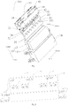
- a film capacitor 100 according to embodiments of the present disclosure will be described with reference to drawings in the following.
- the film capacitor 100 is a three-level film capacitor, which includes: a casing 10, a plurality of capacitor cores 60, a positive electrode busbar 20, a negative electrode busbar 30, an intermediate busbar 40, a first connection sheet 22 connected to the positive electrode busbar 20, a second connection sheet 32 connected to the negative electrode busbar 30, a third connection sheet connected to the intermediate busbar 40, a first electrode terminal 21 connected to the positive electrode busbar 20, a second electrode terminal 31 connected to the negative electrode busbar 30, and a third electrode terminal 41 connected to the intermediate busbar 40.
- the casing 10 has an open upper end, and the plurality of capacitor cores 60, the positive electrode busbar 20, the negative electrode busbar 30, the intermediate busbar 40, the first connection sheet 22, the second connection sheet 32, and the third connection sheet 42 are disposed within the casing 10 and sealed by potting insulators.
- the plurality of capacitor cores 60 includes a first group of capacitor cores 61 and a second group of capacitor cores 62.
- the first group of capacitor cores 61 is connected in parallel, and has a first end surface and a second end surface.
- the second group of capacitor cores 62 is connected in parallel, and has a third end surface and a fourth end surface.
- the second group of capacitor cores 62 is connected with the first group of capacitor cores 61 in series.
- the third end surface of the second group of capacitor cores 62 is opposed to the first end surface of the first group of capacitor cores 61.
- Each capacitor core 60 has a positive electrode and a negative electrode.
- the positive electrodes of the first group of capacitor cores 61 are connected in parallel via the positive electrode busbar 20 and the first connection sheet 22 disposed on the first end surface.
- the negative electrodes of the second group of capacitor cores 62 are connected in parallel via the negative electrode busbar 30 and the second connection sheet 32 disposed on the third end surface.
- the negative electrodes of the first group of capacitor cores 61 are connected with the positive electrodes of the second group of capacitor cores 62 in series via the intermediate busbar 40 and the third connection sheet 42, in which the intermediate busbar 40 and the third connection sheet 42 are disposed on both the second end surface of first group of capacitor cores 61 and the fourth end surface of the second group of capacitor cores 62 respectively.
- the intermediate busbar 40 is provided with a plurality of relief holes 43 configured to expose the first electrode terminal 21 and the second electrode terminal 31 therefrom. Thus the first electrode terminal 21 and the second electrode terminal 31 may pass through the relief holes 43 and may connect with external components.
- the intermediate busbar 40 is connected with the two groups of capacitor cores at the open upper end of the casing 10, i.e., the two groups of capacitor cores are electrically connected with each other via the intermediate busbar 40, and the intermediate busbar 40 is located at the open upper end of the casing 10.
- the upper end of the casing 10 is opened and the casing 10 has a chamber therein.
- the plurality of capacitor cores 60, the positive electrode busbar 20, the negative electrode busbar 30, the intermediate busbar 40, the first connection sheet 22, the second connection sheet 32, and the third connection sheet 42 are disposed within the chamber and sealed by potting insulators.
- the plurality of capacitor cores 60 includes the first group of capacitor cores 61 and the second group of capacitor cores 62 in a front-rear direction.
- a rear end surface (i.e. the first end surface) of the first group of capacitor cores 61 is opposed to a front end surface (i.e. the third end surface) of the second group of capacitor cores 62.
- the positive electrode busbar 20 is disposed on the rear end surface of the first group of capacitor cores 61.
- the positive electrode busbar 20 is provided with a plurality of the first connection sheets 22 connected in parallel, and each of the plurality of the first connection sheets 22 is connected to the rear end surface of the first group of capacitor cores 61 respectively.
- the negative electrode busbar 30 is disposed on the front end surface of the second group of capacitor cores 62, and is insulated from the positive electrode busbar 20 via an insulation sheet 50.
- the negative electrode busbar 30 is provided with a plurality of the second connection sheets 32 connected in parallel, and each of the plurality of the second connection sheets 32 is connected to the front end surface of the second group of capacitor cores 62 respectively.
- the intermediate busbar 40 is disposed above the plurality of capacitor cores 60. Each of front and rear side edges of the intermediate busbar 40 is provided with the third connection sheet 42 respectively.
- a plurality of the third connection sheets 42 is provided at the front side edge of the intermediate busbar 40, located between a front end surface (i.e. the second end surface) of the first group of capacitor cores 61 and a front wall of the casing 10, and connected with the front end surface of the first group of capacitor cores 61 respectively.
- a plurality of the third connection sheets 42 is provided at the rear side edge of the intermediate busbar 40, located between a rear end surface (i.e. the fourth end surface) of the second group of capacitor cores 62 and a rear wall of the casing 10, and connected with the rear end surface of the second group of capacitor cores 62 respectively.
- the plurality of the capacitor cores 60 is divided into two groups, and the capacitor cores in each group are connected in parallel via the positive electrode busbar 20 or the negative electrode busbar 30 respectively, and the two groups are connected in series with each other through the intermediate busbar 40 and the third connection sheet 42, the structure of the film capacitor 100 may be simplified, and the assembling may be convenient. Moreover, a plurality of capacitor cores 60 may be easily connected together in series, and the whole capacity of the film capacitor 100 may be improved.
- the above mentioned structure is suitable for three-level capacitor and has a wide application.
- the intermediate busbar 40 is of a substantial inverted U shape, including a top portion and two free ends.
- the plurality of the third connection sheet 42 is provided with and integrally formed with the two free ends respectively, and the top portion covers above an upper surface of the plurality of capacitor cores 60.
- the third connection sheets 42 disposed at both the front and rear side edges of the intermediate busbar 40 are integrally formed with the intermediate busbar 40.
- the intermediate busbar 40 covers the upper surface of the plurality of capacitor cores 60 and seals the open upper end of the casing 10.
- the intermediate busbar 40 is provided with the third electrode terminal 41 and the plurality of relief holes 43 configured to expose the first electrode terminal 21 and the second electrode terminal 31 therefrom.
- the first electrode terminal 21 and the second electrode terminal 31 may pass through the relief holes 43 and may connect with external components, as shown in Fig. 3 . Therefore, the intermediate busbar 40 has a reasonable structure, and is easy to be molded and assembled, which may reduce the manufacturing costs.
- the plurality of capacitor cores 60 may be arranged according to requirements of the three-level structure. Alternatively, as shown in Fig. 1 , each group of the plurality of capacitor cores 60 (i.e. including the first group of capacitor cores 61 and the second group of capacitor cores 62) is arranged in a plurality of rows and at least one layer. In some embodiments, the plurality of capacitor cores 60 is arranged in two groups, i.e. the first group of capacitor cores 61 and the second group of capacitor cores 62, each group of the plurality of capacitor cores 60 is arranged in the plurality of rows and two layers. Therefore, the plurality of capacitor cores 60 has a reasonable structure and is easy to be assembled, and the whole capacity of the thin-film capacitor 100 is further improved.
- the first connection sheet 22 is provided with a first connection terminal 221 at a peripheral edge thereof
- the second connection sheet 32 is provided with a second connection terminal at a peripheral edge thereof
- the third connection sheet 42 is provided with a third connection terminal 421 at a peripheral edge thereof.
- a plurality of the first connection terminals 221 are provided, disposed at the peripheral edge of the first connection sheet 22 and spaced apart from each other.
- a plurality of the second connection terminals are provided, disposed at the peripheral edge of the second connection sheet 32 and spaced apart from each other.
- a plurality of the third connection terminals 421 are provided, disposed at the peripheral edge of the third connection sheet 42 and spaced apart from each other.
- the plurality of the first connection terminals 221 are disposed on the peripheral edge of the first connection sheet 22, the plurality of the second connection terminals are disposed on the peripheral edge of the second connection sheet 32, and the plurality of the third connection terminals 421 are disposed on the peripheral edge of the third connection sheet 42.
- the first connection sheet 22, the second connection sheet 32 and the third connection sheet 42 may be connected to corresponding capacitor cores 60 through respective connection terminals in a welding manner, which is convenient for the welding automation, and effectively improves the product quality and the assembling efficiency.
- first connection terminal 221 and the first connection sheet 22 are integrally formed, the second connection terminal and the second connection sheet 32 are integrally formed, and the third connection terminal 421 and the third connection sheet 42 are integrally formed.
- first connection sheet 22 and the positive electrode busbar 20 are integrally formed, the second connection sheet 32 and the negative electrode busbar 30 are integrally formed, and the third connection sheet 42 and the intermediate busbar 40 are integrally formed.
- the first connection sheet 22, the first connection terminal 221 and the positive electrode busbar 20 are integrally formed; the second connection sheet 32, the second connection terminal and the negative electrode busbar 30 are integrally formed; the third connection sheet 42, the third connection terminal 421 and the intermediate busbar 40 are integrally formed.
Landscapes
- Engineering & Computer Science (AREA)
- Power Engineering (AREA)
- Microelectronics & Electronic Packaging (AREA)
- Manufacturing & Machinery (AREA)
- Fixed Capacitors And Capacitor Manufacturing Machines (AREA)
Claims (9)
- Condensateur à film (100), comprenant :une pluralité de noyaux de condensateur (60), comprenant :le condensateur à film comprenant en outre :un premier groupe de noyaux de condensateur (61) reliés en parallèle, ayant une première surface d'extrémité et une deuxième surface d'extrémité ; etun second groupe de noyaux de condensateur (62) reliés en parallèle, relié au premier groupe de noyaux de condensateur en série, ayant une troisième surface d'extrémité opposée à la première surface d'extrémité du premier groupe de noyaux de condensateur et une quatrième surface d'extrémité ;une barre omnibus d'électrode positive (20),une barre omnibus d'électrode négative (30), reliée à la troisième surface d'extrémité du second groupe de noyaux de condensateur ;une barre omnibus intermédiaire (40),une première feuille de liaison (22) reliée à la barre omnibus d'électrode positive (20) ;une deuxième feuille de liaison (32) reliée à la barre omnibus d'électrode négative (30) ;une troisième feuille de liaison (42) reliée à la barre omnibus intermédiaire (40),une première borne d'électrode (21) reliée à la barre omnibus d'électrode positive (20) ;une deuxième borne d'électrode (31) reliée à la barre omnibus d'électrode négative (30) ; etune troisième borne d'électrode (41) reliée à la barre omnibus intermédiaire (40),caractérisé en ce quela barre omnibus d'électrode positive (20) est reliée à la première surface d'extrémité du premier groupe de noyaux de condensateur (61), etla barre omnibus intermédiaire (40) est reliée à la deuxième surface d'extrémité du premier groupe de noyaux de condensateur (61) et à la quatrième surface d'extrémité du second groupe de noyaux de condensateur (62) respectivement, et en ce quela barre omnibus intermédiaire (40) est pourvue d'une pluralité de trous de décharge (43) configurés pour exposer la première borne d'électrode (21) et la deuxième borne d'électrode (31) à partir de ceux-ci.
- Condensateur à film selon la revendication 1, comprenant en outre un boîtier (10),
dans lequel la pluralité de noyaux de condensateur (60), la barre omnibus d'électrode positive (20), la barre omnibus d'électrode négative (30), la barre omnibus intermédiaire (40), la première feuille de liaison (22), la deuxième feuille de liaison (32) et la troisième feuille de liaison (42) sont disposées à l'intérieur du boîtier (10) et scellées par des isolants d'enrobage. - Condensateur à film (100) selon l'une quelconque des revendications 1 à 2, comprenant en outre une feuille d'isolation (50) située entre la barre omnibus d'électrode positive (20) et la barre omnibus d'électrode négative (30).
- Condensateur à film (100) selon l'une quelconque des revendications 1 à 3, dans lequel la barre omnibus intermédiaire (40) est sensiblement en forme de U inversé et comprend :deux extrémités libres, chacune pourvue de la troisième feuille de liaison (42) et formée d'un seul tenant avec celle-ci ; etune partie supérieure, en couverture au-dessus d'une surface supérieure de la pluralité de noyaux de condensateur (60).
- Condensateur à film (100) selon l'une quelconque des revendications 1 à 4, dans lequel chaque groupe de noyaux de condensateur (60) est agencé en une pluralité de rangées et au moins une couche.
- Condensateur à film (100) selon la revendication 5, dans lequel chaque groupe de noyaux de condensateur est agencé en la pluralité de rangées et deux couches.
- Condensateur à film (100) selon l'une quelconque des revendications 1 à 6, dans lequel la première feuille de liaison est pourvue d'une première borne de liaison sur un bord périphérique de celle-ci,
la deuxième feuille de liaison (32) est pourvue d'une deuxième borne de liaison sur un bord périphérique de celle-ci,
la troisième feuille de liaison (42) est pourvue d'une troisième borne de liaison sur un bord périphérique de celle-ci. - Condensateur à film (100) selon la revendication 7, dans lequel la première borne de liaison et la première feuille de liaison sont formées d'un seul tenant,
la deuxième borne de liaison et la deuxième feuille de liaison sont formées d'un seul tenant, et
la troisième borne de liaison et la troisième feuille de liaison sont formées d'un seul tenant. - Condensateur à film (100) selon l'une quelconque des revendications 1 à 8, dans lequel la première feuille de liaison (22) et la barre omnibus d'électrode positive (20) sont formées d'un seul tenant,
la deuxième feuille de liaison (32) et la barre omnibus d'électrode négative (30) sont formées d'un seul tenant, et
la troisième feuille de liaison (42) et la barre omnibus intermédiaire (40) sont formées d'un seul tenant.
Applications Claiming Priority (2)
| Application Number | Priority Date | Filing Date | Title |
|---|---|---|---|
| CN201410709201.9A CN105702458B (zh) | 2014-11-28 | 2014-11-28 | 三电平用薄膜电容器 |
| PCT/CN2015/095339 WO2016082730A1 (fr) | 2014-11-28 | 2015-11-23 | Condensateur à film |
Publications (3)
| Publication Number | Publication Date |
|---|---|
| EP3210221A1 EP3210221A1 (fr) | 2017-08-30 |
| EP3210221A4 EP3210221A4 (fr) | 2017-12-13 |
| EP3210221B1 true EP3210221B1 (fr) | 2019-03-06 |
Family
ID=56073606
Family Applications (1)
| Application Number | Title | Priority Date | Filing Date |
|---|---|---|---|
| EP15863867.6A Active EP3210221B1 (fr) | 2014-11-28 | 2015-11-23 | Condensateur à film |
Country Status (6)
| Country | Link |
|---|---|
| US (1) | US10102975B2 (fr) |
| EP (1) | EP3210221B1 (fr) |
| JP (1) | JP6330110B2 (fr) |
| KR (1) | KR101928957B1 (fr) |
| CN (1) | CN105702458B (fr) |
| WO (1) | WO2016082730A1 (fr) |
Families Citing this family (9)
| Publication number | Priority date | Publication date | Assignee | Title |
|---|---|---|---|---|
| US10980911B2 (en) | 2016-01-21 | 2021-04-20 | Global Plasma Solutions, Inc. | Flexible ion generator device |
| US11695259B2 (en) | 2016-08-08 | 2023-07-04 | Global Plasma Solutions, Inc. | Modular ion generator device |
| US11283245B2 (en) | 2016-08-08 | 2022-03-22 | Global Plasma Solutions, Inc. | Modular ion generator device |
| WO2019107128A1 (fr) * | 2017-11-29 | 2019-06-06 | パナソニックIpマネジメント株式会社 | Condensateur |
| JP7169371B2 (ja) | 2018-02-12 | 2022-11-10 | グローバル プラズマ ソリューションズ,インコーポレイテッド | 自己洗浄イオン生成装置 |
| US11581709B2 (en) | 2019-06-07 | 2023-02-14 | Global Plasma Solutions, Inc. | Self-cleaning ion generator device |
| USD875046S1 (en) * | 2019-06-07 | 2020-02-11 | Global Plasma Solutions, Inc. | Self-cleaning ion generator device |
| CN112599355B (zh) * | 2020-12-04 | 2022-04-29 | 上海永铭电子股份有限公司 | 多芯组陶瓷电容器 |
| CN118284471A (zh) | 2021-08-30 | 2024-07-02 | 环球等离子解决方案公司 | 用于产生离子的自清洁装置 |
Family Cites Families (25)
| Publication number | Priority date | Publication date | Assignee | Title |
|---|---|---|---|---|
| JP2003133172A (ja) * | 2001-10-26 | 2003-05-09 | Shizuki Electric Co Inc | スナバコンデンサ |
| JP3914865B2 (ja) | 2002-12-06 | 2007-05-16 | 松下電器産業株式会社 | 金属化フィルムコンデンサ |
| JP2008148530A (ja) * | 2006-12-13 | 2008-06-26 | Toshiba Corp | インバータ装置 |
| US8315031B2 (en) * | 2007-10-12 | 2012-11-20 | Panasonic Corporation | Case mold type capacitor |
| JP2009099884A (ja) * | 2007-10-19 | 2009-05-07 | Toyota Motor Corp | コンデンサ |
| US8018712B2 (en) * | 2008-03-13 | 2011-09-13 | Nuintek Co., Ltd. | Bus-bar for jointing capacitor |
| JP5167922B2 (ja) * | 2008-04-15 | 2013-03-21 | パナソニック株式会社 | ケースモールド型コンデンサ |
| KR100983882B1 (ko) * | 2008-07-07 | 2010-09-27 | 주식회사 뉴인텍 | 커패시터용 부스바 조립방법 및 그 제품 |
| KR101310505B1 (ko) * | 2008-12-10 | 2013-09-25 | 파나소닉 주식회사 | 케이스 몰드형 콘덴서 |
| JP5365919B2 (ja) * | 2009-06-30 | 2013-12-11 | 株式会社指月電機製作所 | コンデンサ |
| US20110149472A1 (en) * | 2009-12-21 | 2011-06-23 | Nuintek Co., Ltd. | Method of connecting busbars with capacitor and product manufactured by the same method |
| KR20110135233A (ko) * | 2010-06-10 | 2011-12-16 | 현대자동차주식회사 | 자동차의 인버터용 커패시터 |
| WO2012098622A1 (fr) * | 2011-01-21 | 2012-07-26 | パナソニック株式会社 | Condensateur du type à boîtier moulé |
| US20130335881A1 (en) * | 2011-03-01 | 2013-12-19 | Toyota Jidosha Kabushiki Kaisha | Capacitor device |
| DE102011104255B4 (de) * | 2011-06-15 | 2013-10-10 | Frako Kondensatoren- Und Anlagenbau Gmbh | Kontaktteil zum Kontaktieren von Stirnkontaktschichten auf den Stirnseiten eines Kondensatorwickels sowie ein- und dreiphasige elektrische Becherkondensatoren mit selbigem |
| JP5887724B2 (ja) * | 2011-06-16 | 2016-03-16 | 株式会社明電舎 | 電源モジュール接続構造 |
| CN202384178U (zh) | 2011-12-07 | 2012-08-15 | 厦门法拉电子股份有限公司 | 一种带有内部叠层母排的电容器结构 |
| JP6061487B2 (ja) * | 2012-04-24 | 2017-01-18 | 住友重機械工業株式会社 | 電力変換装置 |
| JP2013251351A (ja) * | 2012-05-31 | 2013-12-12 | Meidensha Corp | コンデンサ |
| KR101363285B1 (ko) * | 2012-09-04 | 2014-02-17 | 주식회사 뉴인텍 | 분리 유닛형 부스바를 갖는 저인덕턴스형 케이스 탑재식 커패시터 |
| CN102882385B (zh) * | 2012-10-22 | 2015-09-23 | 台达电子工业股份有限公司 | 用于三电平功率变换器的叠层母排结构以及功率变换器 |
| JP6091979B2 (ja) * | 2013-04-25 | 2017-03-08 | ニチコン株式会社 | 金属化フィルムコンデンサおよびその製造方法 |
| CN103680955B (zh) * | 2013-12-21 | 2016-06-15 | 铜陵源丰电子有限责任公司 | 一种便于纵向和横向安装的薄膜电容器 |
| CN103986309A (zh) | 2014-05-23 | 2014-08-13 | 台达电子企业管理(上海)有限公司 | 直流电容模块及其叠层母排结构 |
| US10128045B2 (en) * | 2014-07-02 | 2018-11-13 | Panasonic Intellectual Property Management Co., Ltd. | Film capacitor |
-
2014
- 2014-11-28 CN CN201410709201.9A patent/CN105702458B/zh active Active
-
2015
- 2015-11-23 WO PCT/CN2015/095339 patent/WO2016082730A1/fr not_active Ceased
- 2015-11-23 KR KR1020177012996A patent/KR101928957B1/ko active Active
- 2015-11-23 JP JP2017528471A patent/JP6330110B2/ja active Active
- 2015-11-23 EP EP15863867.6A patent/EP3210221B1/fr active Active
-
2017
- 2017-05-23 US US15/603,171 patent/US10102975B2/en active Active
Non-Patent Citations (1)
| Title |
|---|
| None * |
Also Published As
| Publication number | Publication date |
|---|---|
| WO2016082730A1 (fr) | 2016-06-02 |
| JP6330110B2 (ja) | 2018-05-23 |
| US20170256358A1 (en) | 2017-09-07 |
| US10102975B2 (en) | 2018-10-16 |
| CN105702458B (zh) | 2018-03-13 |
| CN105702458A (zh) | 2016-06-22 |
| KR20170071542A (ko) | 2017-06-23 |
| KR101928957B1 (ko) | 2018-12-13 |
| EP3210221A4 (fr) | 2017-12-13 |
| EP3210221A1 (fr) | 2017-08-30 |
| JP2018500756A (ja) | 2018-01-11 |
Similar Documents
| Publication | Publication Date | Title |
|---|---|---|
| EP3210221B1 (fr) | Condensateur à film | |
| EP3637503B1 (fr) | Module de batterie comprenant un ensemble de barres omnibus | |
| US10109426B2 (en) | Film capacitor | |
| US10153089B2 (en) | Thin-film capacitor for electric vehicle | |
| WO2016082731A1 (fr) | Condensateur à film | |
| US9419261B2 (en) | Battery pack | |
| EP3761390A1 (fr) | Ensemble de connexion et bloc-batterie | |
| EP3790080A1 (fr) | Module de batterie et bloc-batterie | |
| KR20190116252A (ko) | 배터리 모듈 케이싱, 배터리 모듈 및 배터리 | |
| CN105702460B (zh) | 三电平用薄膜电容器 | |
| CN202888267U (zh) | 一种聚合物锂电池组 | |
| CN105702459B (zh) | 三电平用薄膜电容器 | |
| CN116073078A (zh) | 电芯组件和电池包 | |
| CN208272049U (zh) | 锂电池一体式电极结构 | |
| CN105529189B (zh) | 三电平用薄膜电容器 | |
| CN208773523U (zh) | 锂电池摆放装置 | |
| CN114094285B (zh) | 一种单侧极柱长电池及电能存储装置 | |
| CN205752333U (zh) | 电池组 | |
| KR20260040312A (ko) | 배터리 셀, 배터리 장치, 및 전기 디바이스 | |
| JP3052462U (ja) | 高電圧用複合フィルムコンデンサの絶縁構造 |
Legal Events
| Date | Code | Title | Description |
|---|---|---|---|
| STAA | Information on the status of an ep patent application or granted ep patent |
Free format text: STATUS: THE INTERNATIONAL PUBLICATION HAS BEEN MADE |
|
| PUAI | Public reference made under article 153(3) epc to a published international application that has entered the european phase |
Free format text: ORIGINAL CODE: 0009012 |
|
| STAA | Information on the status of an ep patent application or granted ep patent |
Free format text: STATUS: REQUEST FOR EXAMINATION WAS MADE |
|
| 17P | Request for examination filed |
Effective date: 20170523 |
|
| AK | Designated contracting states |
Kind code of ref document: A1 Designated state(s): AL AT BE BG CH CY CZ DE DK EE ES FI FR GB GR HR HU IE IS IT LI LT LU LV MC MK MT NL NO PL PT RO RS SE SI SK SM TR |
|
| AX | Request for extension of the european patent |
Extension state: BA ME |
|
| A4 | Supplementary search report drawn up and despatched |
Effective date: 20171113 |
|
| RIC1 | Information provided on ipc code assigned before grant |
Ipc: H01G 4/228 20060101ALI20171107BHEP Ipc: H01G 4/38 20060101AFI20171107BHEP |
|
| STAA | Information on the status of an ep patent application or granted ep patent |
Free format text: STATUS: EXAMINATION IS IN PROGRESS |
|
| 17Q | First examination report despatched |
Effective date: 20180102 |
|
| DAV | Request for validation of the european patent (deleted) | ||
| DAX | Request for extension of the european patent (deleted) | ||
| GRAP | Despatch of communication of intention to grant a patent |
Free format text: ORIGINAL CODE: EPIDOSNIGR1 |
|
| STAA | Information on the status of an ep patent application or granted ep patent |
Free format text: STATUS: GRANT OF PATENT IS INTENDED |
|
| INTG | Intention to grant announced |
Effective date: 20181024 |
|
| GRAS | Grant fee paid |
Free format text: ORIGINAL CODE: EPIDOSNIGR3 |
|
| GRAA | (expected) grant |
Free format text: ORIGINAL CODE: 0009210 |
|
| STAA | Information on the status of an ep patent application or granted ep patent |
Free format text: STATUS: THE PATENT HAS BEEN GRANTED |
|
| AK | Designated contracting states |
Kind code of ref document: B1 Designated state(s): AL AT BE BG CH CY CZ DE DK EE ES FI FR GB GR HR HU IE IS IT LI LT LU LV MC MK MT NL NO PL PT RO RS SE SI SK SM TR |
|
| REG | Reference to a national code |
Ref country code: GB Ref legal event code: FG4D |
|
| REG | Reference to a national code |
Ref country code: CH Ref legal event code: EP Ref country code: AT Ref legal event code: REF Ref document number: 1105659 Country of ref document: AT Kind code of ref document: T Effective date: 20190315 |
|
| REG | Reference to a national code |
Ref country code: DE Ref legal event code: R096 Ref document number: 602015026094 Country of ref document: DE |
|
| REG | Reference to a national code |
Ref country code: IE Ref legal event code: FG4D |
|
| REG | Reference to a national code |
Ref country code: NL Ref legal event code: MP Effective date: 20190306 |
|
| REG | Reference to a national code |
Ref country code: LT Ref legal event code: MG4D |
|
| PG25 | Lapsed in a contracting state [announced via postgrant information from national office to epo] |
Ref country code: LT Free format text: LAPSE BECAUSE OF FAILURE TO SUBMIT A TRANSLATION OF THE DESCRIPTION OR TO PAY THE FEE WITHIN THE PRESCRIBED TIME-LIMIT Effective date: 20190306 Ref country code: FI Free format text: LAPSE BECAUSE OF FAILURE TO SUBMIT A TRANSLATION OF THE DESCRIPTION OR TO PAY THE FEE WITHIN THE PRESCRIBED TIME-LIMIT Effective date: 20190306 Ref country code: SE Free format text: LAPSE BECAUSE OF FAILURE TO SUBMIT A TRANSLATION OF THE DESCRIPTION OR TO PAY THE FEE WITHIN THE PRESCRIBED TIME-LIMIT Effective date: 20190306 Ref country code: NO Free format text: LAPSE BECAUSE OF FAILURE TO SUBMIT A TRANSLATION OF THE DESCRIPTION OR TO PAY THE FEE WITHIN THE PRESCRIBED TIME-LIMIT Effective date: 20190606 |
|
| PG25 | Lapsed in a contracting state [announced via postgrant information from national office to epo] |
Ref country code: HR Free format text: LAPSE BECAUSE OF FAILURE TO SUBMIT A TRANSLATION OF THE DESCRIPTION OR TO PAY THE FEE WITHIN THE PRESCRIBED TIME-LIMIT Effective date: 20190306 Ref country code: RS Free format text: LAPSE BECAUSE OF FAILURE TO SUBMIT A TRANSLATION OF THE DESCRIPTION OR TO PAY THE FEE WITHIN THE PRESCRIBED TIME-LIMIT Effective date: 20190306 Ref country code: BG Free format text: LAPSE BECAUSE OF FAILURE TO SUBMIT A TRANSLATION OF THE DESCRIPTION OR TO PAY THE FEE WITHIN THE PRESCRIBED TIME-LIMIT Effective date: 20190606 Ref country code: GR Free format text: LAPSE BECAUSE OF FAILURE TO SUBMIT A TRANSLATION OF THE DESCRIPTION OR TO PAY THE FEE WITHIN THE PRESCRIBED TIME-LIMIT Effective date: 20190607 Ref country code: LV Free format text: LAPSE BECAUSE OF FAILURE TO SUBMIT A TRANSLATION OF THE DESCRIPTION OR TO PAY THE FEE WITHIN THE PRESCRIBED TIME-LIMIT Effective date: 20190306 Ref country code: NL Free format text: LAPSE BECAUSE OF FAILURE TO SUBMIT A TRANSLATION OF THE DESCRIPTION OR TO PAY THE FEE WITHIN THE PRESCRIBED TIME-LIMIT Effective date: 20190306 |
|
| REG | Reference to a national code |
Ref country code: AT Ref legal event code: MK05 Ref document number: 1105659 Country of ref document: AT Kind code of ref document: T Effective date: 20190306 |
|
| PG25 | Lapsed in a contracting state [announced via postgrant information from national office to epo] |
Ref country code: SK Free format text: LAPSE BECAUSE OF FAILURE TO SUBMIT A TRANSLATION OF THE DESCRIPTION OR TO PAY THE FEE WITHIN THE PRESCRIBED TIME-LIMIT Effective date: 20190306 Ref country code: EE Free format text: LAPSE BECAUSE OF FAILURE TO SUBMIT A TRANSLATION OF THE DESCRIPTION OR TO PAY THE FEE WITHIN THE PRESCRIBED TIME-LIMIT Effective date: 20190306 Ref country code: RO Free format text: LAPSE BECAUSE OF FAILURE TO SUBMIT A TRANSLATION OF THE DESCRIPTION OR TO PAY THE FEE WITHIN THE PRESCRIBED TIME-LIMIT Effective date: 20190306 Ref country code: CZ Free format text: LAPSE BECAUSE OF FAILURE TO SUBMIT A TRANSLATION OF THE DESCRIPTION OR TO PAY THE FEE WITHIN THE PRESCRIBED TIME-LIMIT Effective date: 20190306 Ref country code: ES Free format text: LAPSE BECAUSE OF FAILURE TO SUBMIT A TRANSLATION OF THE DESCRIPTION OR TO PAY THE FEE WITHIN THE PRESCRIBED TIME-LIMIT Effective date: 20190306 Ref country code: AL Free format text: LAPSE BECAUSE OF FAILURE TO SUBMIT A TRANSLATION OF THE DESCRIPTION OR TO PAY THE FEE WITHIN THE PRESCRIBED TIME-LIMIT Effective date: 20190306 Ref country code: PT Free format text: LAPSE BECAUSE OF FAILURE TO SUBMIT A TRANSLATION OF THE DESCRIPTION OR TO PAY THE FEE WITHIN THE PRESCRIBED TIME-LIMIT Effective date: 20190706 Ref country code: IT Free format text: LAPSE BECAUSE OF FAILURE TO SUBMIT A TRANSLATION OF THE DESCRIPTION OR TO PAY THE FEE WITHIN THE PRESCRIBED TIME-LIMIT Effective date: 20190306 |
|
| PG25 | Lapsed in a contracting state [announced via postgrant information from national office to epo] |
Ref country code: PL Free format text: LAPSE BECAUSE OF FAILURE TO SUBMIT A TRANSLATION OF THE DESCRIPTION OR TO PAY THE FEE WITHIN THE PRESCRIBED TIME-LIMIT Effective date: 20190306 Ref country code: SM Free format text: LAPSE BECAUSE OF FAILURE TO SUBMIT A TRANSLATION OF THE DESCRIPTION OR TO PAY THE FEE WITHIN THE PRESCRIBED TIME-LIMIT Effective date: 20190306 |
|
| REG | Reference to a national code |
Ref country code: DE Ref legal event code: R097 Ref document number: 602015026094 Country of ref document: DE |
|
| PG25 | Lapsed in a contracting state [announced via postgrant information from national office to epo] |
Ref country code: AT Free format text: LAPSE BECAUSE OF FAILURE TO SUBMIT A TRANSLATION OF THE DESCRIPTION OR TO PAY THE FEE WITHIN THE PRESCRIBED TIME-LIMIT Effective date: 20190306 Ref country code: IS Free format text: LAPSE BECAUSE OF FAILURE TO SUBMIT A TRANSLATION OF THE DESCRIPTION OR TO PAY THE FEE WITHIN THE PRESCRIBED TIME-LIMIT Effective date: 20190706 |
|
| PLBE | No opposition filed within time limit |
Free format text: ORIGINAL CODE: 0009261 |
|
| STAA | Information on the status of an ep patent application or granted ep patent |
Free format text: STATUS: NO OPPOSITION FILED WITHIN TIME LIMIT |
|
| PG25 | Lapsed in a contracting state [announced via postgrant information from national office to epo] |
Ref country code: DK Free format text: LAPSE BECAUSE OF FAILURE TO SUBMIT A TRANSLATION OF THE DESCRIPTION OR TO PAY THE FEE WITHIN THE PRESCRIBED TIME-LIMIT Effective date: 20190306 |
|
| 26N | No opposition filed |
Effective date: 20191209 |
|
| PG25 | Lapsed in a contracting state [announced via postgrant information from national office to epo] |
Ref country code: SI Free format text: LAPSE BECAUSE OF FAILURE TO SUBMIT A TRANSLATION OF THE DESCRIPTION OR TO PAY THE FEE WITHIN THE PRESCRIBED TIME-LIMIT Effective date: 20190306 |
|
| PG25 | Lapsed in a contracting state [announced via postgrant information from national office to epo] |
Ref country code: TR Free format text: LAPSE BECAUSE OF FAILURE TO SUBMIT A TRANSLATION OF THE DESCRIPTION OR TO PAY THE FEE WITHIN THE PRESCRIBED TIME-LIMIT Effective date: 20190306 |
|
| REG | Reference to a national code |
Ref country code: CH Ref legal event code: PL |
|
| PG25 | Lapsed in a contracting state [announced via postgrant information from national office to epo] |
Ref country code: LU Free format text: LAPSE BECAUSE OF NON-PAYMENT OF DUE FEES Effective date: 20191123 Ref country code: CH Free format text: LAPSE BECAUSE OF NON-PAYMENT OF DUE FEES Effective date: 20191130 Ref country code: LI Free format text: LAPSE BECAUSE OF NON-PAYMENT OF DUE FEES Effective date: 20191130 Ref country code: MC Free format text: LAPSE BECAUSE OF FAILURE TO SUBMIT A TRANSLATION OF THE DESCRIPTION OR TO PAY THE FEE WITHIN THE PRESCRIBED TIME-LIMIT Effective date: 20190306 |
|
| REG | Reference to a national code |
Ref country code: BE Ref legal event code: MM Effective date: 20191130 |
|
| PG25 | Lapsed in a contracting state [announced via postgrant information from national office to epo] |
Ref country code: IE Free format text: LAPSE BECAUSE OF NON-PAYMENT OF DUE FEES Effective date: 20191123 |
|
| PG25 | Lapsed in a contracting state [announced via postgrant information from national office to epo] |
Ref country code: BE Free format text: LAPSE BECAUSE OF NON-PAYMENT OF DUE FEES Effective date: 20191130 |
|
| PG25 | Lapsed in a contracting state [announced via postgrant information from national office to epo] |
Ref country code: CY Free format text: LAPSE BECAUSE OF FAILURE TO SUBMIT A TRANSLATION OF THE DESCRIPTION OR TO PAY THE FEE WITHIN THE PRESCRIBED TIME-LIMIT Effective date: 20190306 |
|
| PG25 | Lapsed in a contracting state [announced via postgrant information from national office to epo] |
Ref country code: HU Free format text: LAPSE BECAUSE OF FAILURE TO SUBMIT A TRANSLATION OF THE DESCRIPTION OR TO PAY THE FEE WITHIN THE PRESCRIBED TIME-LIMIT; INVALID AB INITIO Effective date: 20151123 Ref country code: MT Free format text: LAPSE BECAUSE OF FAILURE TO SUBMIT A TRANSLATION OF THE DESCRIPTION OR TO PAY THE FEE WITHIN THE PRESCRIBED TIME-LIMIT Effective date: 20190306 |
|
| PG25 | Lapsed in a contracting state [announced via postgrant information from national office to epo] |
Ref country code: MK Free format text: LAPSE BECAUSE OF FAILURE TO SUBMIT A TRANSLATION OF THE DESCRIPTION OR TO PAY THE FEE WITHIN THE PRESCRIBED TIME-LIMIT Effective date: 20190306 |
|
| P01 | Opt-out of the competence of the unified patent court (upc) registered |
Effective date: 20230527 |
|
| PGFP | Annual fee paid to national office [announced via postgrant information from national office to epo] |
Ref country code: DE Payment date: 20251118 Year of fee payment: 11 |
|
| PGFP | Annual fee paid to national office [announced via postgrant information from national office to epo] |
Ref country code: GB Payment date: 20251120 Year of fee payment: 11 |
|
| PGFP | Annual fee paid to national office [announced via postgrant information from national office to epo] |
Ref country code: FR Payment date: 20251120 Year of fee payment: 11 |