EP3210245B1 - Procédé de stratification sous vide pour former un article à revêtement conforme - Google Patents
Procédé de stratification sous vide pour former un article à revêtement conforme Download PDFInfo
- Publication number
- EP3210245B1 EP3210245B1 EP15851759.9A EP15851759A EP3210245B1 EP 3210245 B1 EP3210245 B1 EP 3210245B1 EP 15851759 A EP15851759 A EP 15851759A EP 3210245 B1 EP3210245 B1 EP 3210245B1
- Authority
- EP
- European Patent Office
- Prior art keywords
- lamination layer
- layer
- preformed lamination
- preformed
- vacuum chamber
- Prior art date
- Legal status (The legal status is an assumption and is not a legal conclusion. Google has not performed a legal analysis and makes no representation as to the accuracy of the status listed.)
- Active
Links
Images



Classifications
-
- B—PERFORMING OPERATIONS; TRANSPORTING
- B32—LAYERED PRODUCTS
- B32B—LAYERED PRODUCTS, i.e. PRODUCTS BUILT-UP OF STRATA OF FLAT OR NON-FLAT, e.g. CELLULAR OR HONEYCOMB, FORM
- B32B27/00—Layered products comprising a layer of synthetic resin
- B32B27/30—Layered products comprising a layer of synthetic resin comprising vinyl (co)polymers; comprising acrylic (co)polymers
- B32B27/306—Layered products comprising a layer of synthetic resin comprising vinyl (co)polymers; comprising acrylic (co)polymers comprising vinyl acetate or vinyl alcohol (co)polymers
-
- H—ELECTRICITY
- H10—SEMICONDUCTOR DEVICES; ELECTRIC SOLID-STATE DEVICES NOT OTHERWISE PROVIDED FOR
- H10H—INORGANIC LIGHT-EMITTING SEMICONDUCTOR DEVICES HAVING POTENTIAL BARRIERS
- H10H20/00—Individual inorganic light-emitting semiconductor devices having potential barriers, e.g. light-emitting diodes [LED]
- H10H20/80—Constructional details
- H10H20/84—Coatings, e.g. passivation layers or antireflective coatings
-
- H—ELECTRICITY
- H10—SEMICONDUCTOR DEVICES; ELECTRIC SOLID-STATE DEVICES NOT OTHERWISE PROVIDED FOR
- H10H—INORGANIC LIGHT-EMITTING SEMICONDUCTOR DEVICES HAVING POTENTIAL BARRIERS
- H10H20/00—Individual inorganic light-emitting semiconductor devices having potential barriers, e.g. light-emitting diodes [LED]
- H10H20/80—Constructional details
- H10H20/85—Packages
- H10H20/852—Encapsulations
- H10H20/853—Encapsulations characterised by their shape
-
- B—PERFORMING OPERATIONS; TRANSPORTING
- B32—LAYERED PRODUCTS
- B32B—LAYERED PRODUCTS, i.e. PRODUCTS BUILT-UP OF STRATA OF FLAT OR NON-FLAT, e.g. CELLULAR OR HONEYCOMB, FORM
- B32B27/00—Layered products comprising a layer of synthetic resin
- B32B27/06—Layered products comprising a layer of synthetic resin as the main or only constituent of a layer, which is next to another layer of the same or of a different material
- B32B27/08—Layered products comprising a layer of synthetic resin as the main or only constituent of a layer, which is next to another layer of the same or of a different material of synthetic resin
-
- B—PERFORMING OPERATIONS; TRANSPORTING
- B32—LAYERED PRODUCTS
- B32B—LAYERED PRODUCTS, i.e. PRODUCTS BUILT-UP OF STRATA OF FLAT OR NON-FLAT, e.g. CELLULAR OR HONEYCOMB, FORM
- B32B27/00—Layered products comprising a layer of synthetic resin
- B32B27/28—Layered products comprising a layer of synthetic resin comprising synthetic resins not wholly covered by any one of the sub-groups B32B27/30 - B32B27/42
- B32B27/283—Layered products comprising a layer of synthetic resin comprising synthetic resins not wholly covered by any one of the sub-groups B32B27/30 - B32B27/42 comprising polysiloxanes
-
- B—PERFORMING OPERATIONS; TRANSPORTING
- B32—LAYERED PRODUCTS
- B32B—LAYERED PRODUCTS, i.e. PRODUCTS BUILT-UP OF STRATA OF FLAT OR NON-FLAT, e.g. CELLULAR OR HONEYCOMB, FORM
- B32B27/00—Layered products comprising a layer of synthetic resin
- B32B27/30—Layered products comprising a layer of synthetic resin comprising vinyl (co)polymers; comprising acrylic (co)polymers
- B32B27/302—Layered products comprising a layer of synthetic resin comprising vinyl (co)polymers; comprising acrylic (co)polymers comprising aromatic vinyl (co)polymers, e.g. styrenic (co)polymers
-
- B—PERFORMING OPERATIONS; TRANSPORTING
- B32—LAYERED PRODUCTS
- B32B—LAYERED PRODUCTS, i.e. PRODUCTS BUILT-UP OF STRATA OF FLAT OR NON-FLAT, e.g. CELLULAR OR HONEYCOMB, FORM
- B32B27/00—Layered products comprising a layer of synthetic resin
- B32B27/30—Layered products comprising a layer of synthetic resin comprising vinyl (co)polymers; comprising acrylic (co)polymers
- B32B27/308—Layered products comprising a layer of synthetic resin comprising vinyl (co)polymers; comprising acrylic (co)polymers comprising acrylic (co)polymers
-
- B—PERFORMING OPERATIONS; TRANSPORTING
- B32—LAYERED PRODUCTS
- B32B—LAYERED PRODUCTS, i.e. PRODUCTS BUILT-UP OF STRATA OF FLAT OR NON-FLAT, e.g. CELLULAR OR HONEYCOMB, FORM
- B32B27/00—Layered products comprising a layer of synthetic resin
- B32B27/32—Layered products comprising a layer of synthetic resin comprising polyolefins
-
- B—PERFORMING OPERATIONS; TRANSPORTING
- B32—LAYERED PRODUCTS
- B32B—LAYERED PRODUCTS, i.e. PRODUCTS BUILT-UP OF STRATA OF FLAT OR NON-FLAT, e.g. CELLULAR OR HONEYCOMB, FORM
- B32B27/00—Layered products comprising a layer of synthetic resin
- B32B27/38—Layered products comprising a layer of synthetic resin comprising epoxy resins
-
- B—PERFORMING OPERATIONS; TRANSPORTING
- B32—LAYERED PRODUCTS
- B32B—LAYERED PRODUCTS, i.e. PRODUCTS BUILT-UP OF STRATA OF FLAT OR NON-FLAT, e.g. CELLULAR OR HONEYCOMB, FORM
- B32B3/00—Layered products comprising a layer with external or internal discontinuities or unevennesses, or a layer of non-planar shape; Layered products comprising a layer having particular features of form
- B32B3/26—Layered products comprising a layer with external or internal discontinuities or unevennesses, or a layer of non-planar shape; Layered products comprising a layer having particular features of form characterised by a particular shape of the outline of the cross-section of a continuous layer; characterised by a layer with cavities or internal voids ; characterised by an apertured layer
- B32B3/28—Layered products comprising a layer with external or internal discontinuities or unevennesses, or a layer of non-planar shape; Layered products comprising a layer having particular features of form characterised by a particular shape of the outline of the cross-section of a continuous layer; characterised by a layer with cavities or internal voids ; characterised by an apertured layer characterised by a layer comprising a deformed thin sheet, i.e. the layer having its entire thickness deformed out of the plane, e.g. corrugated, crumpled
-
- B—PERFORMING OPERATIONS; TRANSPORTING
- B32—LAYERED PRODUCTS
- B32B—LAYERED PRODUCTS, i.e. PRODUCTS BUILT-UP OF STRATA OF FLAT OR NON-FLAT, e.g. CELLULAR OR HONEYCOMB, FORM
- B32B37/00—Methods or apparatus for laminating, e.g. by curing or by ultrasonic bonding
- B32B37/10—Methods or apparatus for laminating, e.g. by curing or by ultrasonic bonding characterised by the pressing technique, e.g. using action of vacuum or fluid pressure
- B32B37/1018—Methods or apparatus for laminating, e.g. by curing or by ultrasonic bonding characterised by the pressing technique, e.g. using action of vacuum or fluid pressure using only vacuum
-
- B—PERFORMING OPERATIONS; TRANSPORTING
- B32—LAYERED PRODUCTS
- B32B—LAYERED PRODUCTS, i.e. PRODUCTS BUILT-UP OF STRATA OF FLAT OR NON-FLAT, e.g. CELLULAR OR HONEYCOMB, FORM
- B32B5/00—Layered products characterised by the non- homogeneity or physical structure, i.e. comprising a fibrous, filamentary, particulate or foam layer; Layered products characterised by having a layer differing constitutionally or physically in different parts
- B32B5/16—Layered products characterised by the non- homogeneity or physical structure, i.e. comprising a fibrous, filamentary, particulate or foam layer; Layered products characterised by having a layer differing constitutionally or physically in different parts characterised by features of a layer formed of particles, e.g. chips, powder or granules
-
- B—PERFORMING OPERATIONS; TRANSPORTING
- B32—LAYERED PRODUCTS
- B32B—LAYERED PRODUCTS, i.e. PRODUCTS BUILT-UP OF STRATA OF FLAT OR NON-FLAT, e.g. CELLULAR OR HONEYCOMB, FORM
- B32B5/00—Layered products characterised by the non- homogeneity or physical structure, i.e. comprising a fibrous, filamentary, particulate or foam layer; Layered products characterised by having a layer differing constitutionally or physically in different parts
- B32B5/22—Layered products characterised by the non- homogeneity or physical structure, i.e. comprising a fibrous, filamentary, particulate or foam layer; Layered products characterised by having a layer differing constitutionally or physically in different parts characterised by the presence of two or more layers which are next to each other and are fibrous, filamentary, formed of particles or foamed
- B32B5/30—Layered products characterised by the non- homogeneity or physical structure, i.e. comprising a fibrous, filamentary, particulate or foam layer; Layered products characterised by having a layer differing constitutionally or physically in different parts characterised by the presence of two or more layers which are next to each other and are fibrous, filamentary, formed of particles or foamed one layer being formed of particles, e.g. chips, granules, powder
-
- H—ELECTRICITY
- H10—SEMICONDUCTOR DEVICES; ELECTRIC SOLID-STATE DEVICES NOT OTHERWISE PROVIDED FOR
- H10H—INORGANIC LIGHT-EMITTING SEMICONDUCTOR DEVICES HAVING POTENTIAL BARRIERS
- H10H20/00—Individual inorganic light-emitting semiconductor devices having potential barriers, e.g. light-emitting diodes [LED]
- H10H20/01—Manufacture or treatment
-
- H—ELECTRICITY
- H10—SEMICONDUCTOR DEVICES; ELECTRIC SOLID-STATE DEVICES NOT OTHERWISE PROVIDED FOR
- H10H—INORGANIC LIGHT-EMITTING SEMICONDUCTOR DEVICES HAVING POTENTIAL BARRIERS
- H10H20/00—Individual inorganic light-emitting semiconductor devices having potential barriers, e.g. light-emitting diodes [LED]
- H10H20/01—Manufacture or treatment
- H10H20/034—Manufacture or treatment of coatings
-
- H—ELECTRICITY
- H10—SEMICONDUCTOR DEVICES; ELECTRIC SOLID-STATE DEVICES NOT OTHERWISE PROVIDED FOR
- H10H—INORGANIC LIGHT-EMITTING SEMICONDUCTOR DEVICES HAVING POTENTIAL BARRIERS
- H10H20/00—Individual inorganic light-emitting semiconductor devices having potential barriers, e.g. light-emitting diodes [LED]
- H10H20/80—Constructional details
- H10H20/85—Packages
- H10H20/851—Wavelength conversion means
-
- H—ELECTRICITY
- H10—SEMICONDUCTOR DEVICES; ELECTRIC SOLID-STATE DEVICES NOT OTHERWISE PROVIDED FOR
- H10H—INORGANIC LIGHT-EMITTING SEMICONDUCTOR DEVICES HAVING POTENTIAL BARRIERS
- H10H20/00—Individual inorganic light-emitting semiconductor devices having potential barriers, e.g. light-emitting diodes [LED]
- H10H20/80—Constructional details
- H10H20/85—Packages
- H10H20/851—Wavelength conversion means
- H10H20/8511—Wavelength conversion means characterised by their material, e.g. binder
- H10H20/8512—Wavelength conversion materials
-
- H—ELECTRICITY
- H10—SEMICONDUCTOR DEVICES; ELECTRIC SOLID-STATE DEVICES NOT OTHERWISE PROVIDED FOR
- H10H—INORGANIC LIGHT-EMITTING SEMICONDUCTOR DEVICES HAVING POTENTIAL BARRIERS
- H10H20/00—Individual inorganic light-emitting semiconductor devices having potential barriers, e.g. light-emitting diodes [LED]
- H10H20/80—Constructional details
- H10H20/85—Packages
- H10H20/851—Wavelength conversion means
- H10H20/8515—Wavelength conversion means not being in contact with the bodies
-
- H—ELECTRICITY
- H10—SEMICONDUCTOR DEVICES; ELECTRIC SOLID-STATE DEVICES NOT OTHERWISE PROVIDED FOR
- H10H—INORGANIC LIGHT-EMITTING SEMICONDUCTOR DEVICES HAVING POTENTIAL BARRIERS
- H10H20/00—Individual inorganic light-emitting semiconductor devices having potential barriers, e.g. light-emitting diodes [LED]
- H10H20/80—Constructional details
- H10H20/85—Packages
- H10H20/852—Encapsulations
-
- H—ELECTRICITY
- H10—SEMICONDUCTOR DEVICES; ELECTRIC SOLID-STATE DEVICES NOT OTHERWISE PROVIDED FOR
- H10W—GENERIC PACKAGES, INTERCONNECTIONS, CONNECTORS OR OTHER CONSTRUCTIONAL DETAILS OF DEVICES COVERED BY CLASS H10
- H10W72/00—Interconnections or connectors in packages
- H10W72/01—Manufacture or treatment
- H10W72/0198—Manufacture or treatment batch processes
-
- H—ELECTRICITY
- H10—SEMICONDUCTOR DEVICES; ELECTRIC SOLID-STATE DEVICES NOT OTHERWISE PROVIDED FOR
- H10W—GENERIC PACKAGES, INTERCONNECTIONS, CONNECTORS OR OTHER CONSTRUCTIONAL DETAILS OF DEVICES COVERED BY CLASS H10
- H10W90/00—Package configurations
-
- B—PERFORMING OPERATIONS; TRANSPORTING
- B32—LAYERED PRODUCTS
- B32B—LAYERED PRODUCTS, i.e. PRODUCTS BUILT-UP OF STRATA OF FLAT OR NON-FLAT, e.g. CELLULAR OR HONEYCOMB, FORM
- B32B2260/00—Layered product comprising an impregnated, embedded, or bonded layer wherein the layer comprises an impregnation, embedding, or binder material
- B32B2260/02—Composition of the impregnated, bonded or embedded layer
- B32B2260/025—Particulate layer
-
- B—PERFORMING OPERATIONS; TRANSPORTING
- B32—LAYERED PRODUCTS
- B32B—LAYERED PRODUCTS, i.e. PRODUCTS BUILT-UP OF STRATA OF FLAT OR NON-FLAT, e.g. CELLULAR OR HONEYCOMB, FORM
- B32B2260/00—Layered product comprising an impregnated, embedded, or bonded layer wherein the layer comprises an impregnation, embedding, or binder material
- B32B2260/04—Impregnation, embedding, or binder material
- B32B2260/046—Synthetic resin
-
- B—PERFORMING OPERATIONS; TRANSPORTING
- B32—LAYERED PRODUCTS
- B32B—LAYERED PRODUCTS, i.e. PRODUCTS BUILT-UP OF STRATA OF FLAT OR NON-FLAT, e.g. CELLULAR OR HONEYCOMB, FORM
- B32B2264/00—Composition or properties of particles which form a particulate layer or are present as additives
- B32B2264/10—Inorganic particles
-
- B—PERFORMING OPERATIONS; TRANSPORTING
- B32—LAYERED PRODUCTS
- B32B—LAYERED PRODUCTS, i.e. PRODUCTS BUILT-UP OF STRATA OF FLAT OR NON-FLAT, e.g. CELLULAR OR HONEYCOMB, FORM
- B32B2307/00—Properties of the layers or laminate
- B32B2307/40—Properties of the layers or laminate having particular optical properties
-
- B—PERFORMING OPERATIONS; TRANSPORTING
- B32—LAYERED PRODUCTS
- B32B—LAYERED PRODUCTS, i.e. PRODUCTS BUILT-UP OF STRATA OF FLAT OR NON-FLAT, e.g. CELLULAR OR HONEYCOMB, FORM
- B32B2307/00—Properties of the layers or laminate
- B32B2307/50—Properties of the layers or laminate having particular mechanical properties
- B32B2307/536—Hardness
-
- B—PERFORMING OPERATIONS; TRANSPORTING
- B32—LAYERED PRODUCTS
- B32B—LAYERED PRODUCTS, i.e. PRODUCTS BUILT-UP OF STRATA OF FLAT OR NON-FLAT, e.g. CELLULAR OR HONEYCOMB, FORM
- B32B2307/00—Properties of the layers or laminate
- B32B2307/50—Properties of the layers or laminate having particular mechanical properties
- B32B2307/546—Flexural strength; Flexion stiffness
-
- B—PERFORMING OPERATIONS; TRANSPORTING
- B32—LAYERED PRODUCTS
- B32B—LAYERED PRODUCTS, i.e. PRODUCTS BUILT-UP OF STRATA OF FLAT OR NON-FLAT, e.g. CELLULAR OR HONEYCOMB, FORM
- B32B2307/00—Properties of the layers or laminate
- B32B2307/70—Other properties
- B32B2307/71—Resistive to light or to UV
-
- B—PERFORMING OPERATIONS; TRANSPORTING
- B32—LAYERED PRODUCTS
- B32B—LAYERED PRODUCTS, i.e. PRODUCTS BUILT-UP OF STRATA OF FLAT OR NON-FLAT, e.g. CELLULAR OR HONEYCOMB, FORM
- B32B2307/00—Properties of the layers or laminate
- B32B2307/70—Other properties
- B32B2307/732—Dimensional properties
-
- B—PERFORMING OPERATIONS; TRANSPORTING
- B32—LAYERED PRODUCTS
- B32B—LAYERED PRODUCTS, i.e. PRODUCTS BUILT-UP OF STRATA OF FLAT OR NON-FLAT, e.g. CELLULAR OR HONEYCOMB, FORM
- B32B2309/00—Parameters for the laminating or treatment process; Apparatus details
- B32B2309/02—Temperature
-
- B—PERFORMING OPERATIONS; TRANSPORTING
- B32—LAYERED PRODUCTS
- B32B—LAYERED PRODUCTS, i.e. PRODUCTS BUILT-UP OF STRATA OF FLAT OR NON-FLAT, e.g. CELLULAR OR HONEYCOMB, FORM
- B32B2309/00—Parameters for the laminating or treatment process; Apparatus details
- B32B2309/04—Time
-
- B—PERFORMING OPERATIONS; TRANSPORTING
- B32—LAYERED PRODUCTS
- B32B—LAYERED PRODUCTS, i.e. PRODUCTS BUILT-UP OF STRATA OF FLAT OR NON-FLAT, e.g. CELLULAR OR HONEYCOMB, FORM
- B32B2309/00—Parameters for the laminating or treatment process; Apparatus details
- B32B2309/12—Pressure
-
- B—PERFORMING OPERATIONS; TRANSPORTING
- B32—LAYERED PRODUCTS
- B32B—LAYERED PRODUCTS, i.e. PRODUCTS BUILT-UP OF STRATA OF FLAT OR NON-FLAT, e.g. CELLULAR OR HONEYCOMB, FORM
- B32B2419/00—Buildings or parts thereof
-
- B—PERFORMING OPERATIONS; TRANSPORTING
- B32—LAYERED PRODUCTS
- B32B—LAYERED PRODUCTS, i.e. PRODUCTS BUILT-UP OF STRATA OF FLAT OR NON-FLAT, e.g. CELLULAR OR HONEYCOMB, FORM
- B32B2457/00—Electrical equipment
-
- B—PERFORMING OPERATIONS; TRANSPORTING
- B32—LAYERED PRODUCTS
- B32B—LAYERED PRODUCTS, i.e. PRODUCTS BUILT-UP OF STRATA OF FLAT OR NON-FLAT, e.g. CELLULAR OR HONEYCOMB, FORM
- B32B2457/00—Electrical equipment
- B32B2457/14—Semiconductor wafers
-
- B—PERFORMING OPERATIONS; TRANSPORTING
- B32—LAYERED PRODUCTS
- B32B—LAYERED PRODUCTS, i.e. PRODUCTS BUILT-UP OF STRATA OF FLAT OR NON-FLAT, e.g. CELLULAR OR HONEYCOMB, FORM
- B32B2457/00—Electrical equipment
- B32B2457/20—Displays, e.g. liquid crystal displays, plasma displays
-
- B—PERFORMING OPERATIONS; TRANSPORTING
- B32—LAYERED PRODUCTS
- B32B—LAYERED PRODUCTS, i.e. PRODUCTS BUILT-UP OF STRATA OF FLAT OR NON-FLAT, e.g. CELLULAR OR HONEYCOMB, FORM
- B32B2605/00—Vehicles
-
- B—PERFORMING OPERATIONS; TRANSPORTING
- B32—LAYERED PRODUCTS
- B32B—LAYERED PRODUCTS, i.e. PRODUCTS BUILT-UP OF STRATA OF FLAT OR NON-FLAT, e.g. CELLULAR OR HONEYCOMB, FORM
- B32B37/00—Methods or apparatus for laminating, e.g. by curing or by ultrasonic bonding
- B32B37/0007—Methods or apparatus for laminating, e.g. by curing or by ultrasonic bonding involving treatment or provisions in order to avoid deformation or air inclusion, e.g. to improve surface quality
- B32B37/003—Methods or apparatus for laminating, e.g. by curing or by ultrasonic bonding involving treatment or provisions in order to avoid deformation or air inclusion, e.g. to improve surface quality to avoid air inclusion
-
- B—PERFORMING OPERATIONS; TRANSPORTING
- B32—LAYERED PRODUCTS
- B32B—LAYERED PRODUCTS, i.e. PRODUCTS BUILT-UP OF STRATA OF FLAT OR NON-FLAT, e.g. CELLULAR OR HONEYCOMB, FORM
- B32B38/00—Ancillary operations in connection with laminating processes
- B32B38/10—Removing layers, or parts of layers, mechanically or chemically
-
- B—PERFORMING OPERATIONS; TRANSPORTING
- B32—LAYERED PRODUCTS
- B32B—LAYERED PRODUCTS, i.e. PRODUCTS BUILT-UP OF STRATA OF FLAT OR NON-FLAT, e.g. CELLULAR OR HONEYCOMB, FORM
- B32B38/00—Ancillary operations in connection with laminating processes
- B32B38/18—Handling of layers or the laminate
- B32B38/1866—Handling of layers or the laminate conforming the layers or laminate to a convex or concave profile
-
- H—ELECTRICITY
- H10—SEMICONDUCTOR DEVICES; ELECTRIC SOLID-STATE DEVICES NOT OTHERWISE PROVIDED FOR
- H10H—INORGANIC LIGHT-EMITTING SEMICONDUCTOR DEVICES HAVING POTENTIAL BARRIERS
- H10H20/00—Individual inorganic light-emitting semiconductor devices having potential barriers, e.g. light-emitting diodes [LED]
- H10H20/01—Manufacture or treatment
- H10H20/036—Manufacture or treatment of packages
- H10H20/0361—Manufacture or treatment of packages of wavelength conversion means
-
- H—ELECTRICITY
- H10—SEMICONDUCTOR DEVICES; ELECTRIC SOLID-STATE DEVICES NOT OTHERWISE PROVIDED FOR
- H10H—INORGANIC LIGHT-EMITTING SEMICONDUCTOR DEVICES HAVING POTENTIAL BARRIERS
- H10H20/00—Individual inorganic light-emitting semiconductor devices having potential barriers, e.g. light-emitting diodes [LED]
- H10H20/01—Manufacture or treatment
- H10H20/036—Manufacture or treatment of packages
- H10H20/0362—Manufacture or treatment of packages of encapsulations
-
- H—ELECTRICITY
- H10—SEMICONDUCTOR DEVICES; ELECTRIC SOLID-STATE DEVICES NOT OTHERWISE PROVIDED FOR
- H10H—INORGANIC LIGHT-EMITTING SEMICONDUCTOR DEVICES HAVING POTENTIAL BARRIERS
- H10H20/00—Individual inorganic light-emitting semiconductor devices having potential barriers, e.g. light-emitting diodes [LED]
- H10H20/80—Constructional details
- H10H20/85—Packages
- H10H20/851—Wavelength conversion means
- H10H20/8511—Wavelength conversion means characterised by their material, e.g. binder
Definitions
- This invention generally provides a method for forming a conformally coated article, and the conformally coated article formed therefrom. More specifically, the method comprises a vacuum lamination method.
- a variety of coated articles can be fabricated by vacuum lamination for a variety of applications such as electronics, building, vehicle, healthcare, and consumer applications.
- some electronics applications use coated electronic devices such as coated light emitting diodes.
- Light emitting diode (LED) devices including an array of light emitting diodes (LEDs) coupled to a substrate can be fabricated to generate light in different colors.
- One way for producing light of different colors or for otherwise controlling or manipulating the light generated from the LEDs is to deposit a phosphor material over the array of LEDs. There are many ways to do this.
- One of the most common ways is to dispense a mixture of phosphor and encapsulant over the LEDs.
- the lamination method commonly used is a vacuum lamination technique that includes two distinct heating steps, hereinafter referred to as a two-step vacuum lamination technique or method.
- Patent application document WO 2012/023119 discloses a vacuum lamination method of LED devices on a carrier substrate. This vacuum lamination method involved two independent heating steps.
- the preformed lamination layer is first heated to temperatures high enough to achieve flow in the uncured thermosetting binder material, followed by a second heating step wherein the preformed lamination layer is reheated and conformally coated to the LED array.
- the preformed laminated layer begins to cure (i.e., crosslink), therein reducing the flow characteristics of the layer, and hence the layer may be too stiff to be subsequently conformed during the second final heating step or, alternatively may be conformed but with substantial defects associated therewith.
- the processing time encompassing the second heating step and subsequent conforming of the preformed lamination layer over the array of LEDs is limited due to the partial curing of the binder material in the first heating step.
- the limited processing time during the second heating step and subsequent conformation step does not allow the two-step vacuum lamination technique to be used on arrays of LEDs of varying heights, and also limits the choices for binder materials and phosphor materials that may be used in two-step vacuum lamination techniques based upon this limited processing time.
- the present invention addresses many of the problems with lamination techniques utilizing two-step vacuum lamination technique described above.
- the present invention discloses vacuum lamination methods for forming conformally coated articles by vacuum lamination for a variety of applications such as consumer, healthcare, building, vehicle, and electronics applications such as light emitting diode (LED) devices.
- applications such as consumer, healthcare, building, vehicle, and electronics applications such as light emitting diode (LED) devices.
- LED light emitting diode
- this invention is a method of fabricating a conformally coated article from an assembly that is housed in a vacuum chamber of a fabrication device; Wherein the vacuum chamber contains an applied vacuum; Wherein the assembly comprises a preformed lamination layer and an object having a surface in need of lamination; Wherein the preformed lamination layer has a first surface and a second surface opposite the first surface, and a heat-softened middle portion at a first temperature and surrounded by an edge portion; Wherein the object has a first surface and a second surface opposite the first surface, and the first surface being in need of lamination and comprising an inner portion and a perimeter portion surrounding the inner portion; Wherein the assembly is configured such that the first surface of the preformed lamination layer is positioned facing the first surface of the object, wherein the edge portion of the preformed lamination layer forms a gastight seal to the perimeter portion of the first surface of the object such that the assembly contains a gastight inner region defined by a combination of the gas
- LED devices having a plurality of light emitting diodes (LEDs) and a preformed lamination layer conformally coated to an LED array in which a single heating step is utilized to heat the middle portion of the preformed lamination layer prior to the preformed lamination layer being conformally coated over the array of LEDs disposed on a first side of a substrate, e.g., a submount wafer.
- LEDs light emitting diodes
- the method includes: (A) mounting a preformed lamination layer having a first surface and a second surface over an LED array; (B) adhering a portion of the edge portion of the preformed lamination layer to the perimeter portion of the first side of the substrate, e.g., a submount wafer; (C) introducing the LED array and the preformed lamination layer to the vacuum chamber; (D) after step (C), applying a vacuum within the vacuum chamber and heating the preformed lamination layer to a first temperature sufficient to soften the edge portion and the middle portion of the preformed lamination layer; (E) sealing the softened edge portion to the perimeter portion under the applied vacuum to create an gastight seal there between, thereby creating an gastight inner region defined by the gastight seal, the first surface of the preformed lamination
- the method includes: (A) mounting a preformed lamination layer having a first surface and a second surface over an LED array; (B) introducing the LED array and the preformed lamination layer to the vacuum chamber; (C) after step (B), applying a vacuum within the vacuum chamber; (D) sealing the edge portion to the perimeter portion under the applied vacuum to create an gastight seal there between, thereby creating an gastight inner region defined by the gastight seal, the first surface of the preformed lamination layer and the first side of the substrate, e.g., a submount wafer; (E) after step (D), heating the preformed lamination layer to a first temperature sufficient to soften the middle portion of the preformed lamination layer; and (F) conforming the softened preformed lamination layer over the LED array by increasing the gas pressure within the vacuum chamber in an area not defined by the gastight inner region to a pressure greater than the gas pressure within the gastight inner region.
- the vacuum lamination methods of the present invention forms generally defect free conformal coatings on the LED arrays in a simple and repeatable manner.
- the processing window for applying and conforming the lamination layer is increased as compared to two-step vacuum lamination techniques in the prior art in which two distinct heating steps are utilized.
- This allows the use of preformed lamination layers having different phosphor levels, in combination with additional or differing binder compositions having varying rheologies or cure speeds, to be formed in the same fabrication device that cannot be utilized in two-step vacuum lamination techniques due to the limited processing window.
- the method of the present invention allows for the conformal coating over arrays of LEDs having varying heights due to this increased processing window which is not available in two-step vacuum lamination techniques.
- the heat-softened middle portion of the preformed lamination layer is obtained by heating the middle portion of the preformed lamination layer to the first temperature in a single heating step prior to the preformed lamination layer being conformally coated over the object such as the LEDs.
- the preformed lamination layer may be composed of any material that can sequentially be heat-softened, sealed under vacuum to a surface of an object to form a gastight inner region, and conformed to the surface of the object.
- the preformed lamination layer is composed of a thermoplastic or thermosetting material.
- Such material may be an organic polymer or a silicone.
- the organic polymer may be a thermoplastic or thermosetting macromolecular material such as a polyolefin, an ethyl vinyl acetate (EVA), an epoxy, a polyacrylate, or a poly(vinyl butyral).
- the silicone may be a thermoplastic or thermosetting macromolecular material such as a hot melt silicone or a resin-linear silicone.
- the silicone may be curable such as by condensation, hydrosilylation, or free radical curing.
- the material of the preformed lamination layer is a hydrosilylation curable silicone, alternatively condensation curable, alternatively free radical curable.
- the material of the preformed lamination layer is composed of a thermoplastic material.
- the material of the preformed lamination layer is composed of a thermosetting material.
- the material of the preformed lamination layer may also be chosen based on it having one or more additional properties suitable for such an application.
- adhesion adhesion
- optical transmittance modulus
- hardness compatibility with an optional constituent such as a finely divided filler or phosphor
- resistance to yellowing or oxidizing resistance to degradation caused by prolonged exposure to heat and/or light.
- reduced gas pressure means a force exerted by a gaseous or vaporous substance in a volumetric space or region that is housed within a vacuum chamber, wherein the force is less than ambient gas pressure (i.e., the force that existed prior to the applying a vacuum step).
- the means of lowering the force comprises applying a vacuum, i.e., placing the vacuum chamber and volumetric space in fluidic communication with a vacuum source, such as an operating vacuum pump.
- the vacuum chamber has a controllable pressure region which is in fluidic communication with the vacuum source or with a source of gas that is external to the vacuum chamber.
- the source of gas may be air atmosphere; an inert gas source such as a source of gaseous nitrogen, helium or argon; or, if desired, a treatment gas such as gaseous hydrogen, oxygen, monosilane, or the like.
- the phrase "the applied vacuum in the vacuum chamber is effectively equal to the reduced gas pressure in the gastight inner region of the assembly" means that in some embodiments the applied vacuum is equal to the reduced gas pressure and in other embodiments that the reduced gas pressure in the gastight inner region of the assembly is slightly different (e.g., ⁇ 0.1 kilopascals) than the applied vacuum in the vacuum chamber, but not so much higher as to cause the preformed lamination layer to bulge or puff and result in process failure and not so much lower as to cause the preformed lamination layer to contact the inner portion of the first surface of the object to be conformally coated.
- a Markush group of members A, B, and C may be equivalently expressed as: "a member selected from A, B, and C"; "a member selected from the group consisting of A, B, and C”; or "a member A, B, or C".
- the Markush group may comprise two or more of a genus, a subgenus thereof, and one or more specific members thereof; each of which may be relied upon individually or collectively and provides adequate support for specific inventive embodiments.
- any reference to "greater than”, as in greater than a specified individual number encompasses a range or subrange that includes as its upper endpoint the absolute maximum (e.g., 100%) or, as the case may be where there is no absolute maximum, a practical maximum (e.g., 10,000 repeat units or 10,000,000 g/mol.
- the upper endpoint may be less than the absolute maximum (e.g., ⁇ 100%) or less than the practical maximum (e.g., ⁇ 10,000 repeat units or ⁇ 10,000,000 g/mol).
- any reference to "less than”, as in less than a specified individual number encompasses a range or subrange that includes as its lower endpoint the absolute minimum (e.g., zero (0)) or, as the case may be where there is no absolute minimum, a practical minimum (e.g., greater than zero (> 0).
- a practical minimum > 0 is clear from the context of the expression "present at a concentration less than 10 wt%”.
- the lower endpoint may be greater than the absolute minimum (e.g., > 0%).
- May confers a choice, not an imperative.
- “Operative” means functionally effective.
- operative contact comprises functionally effective touching, e.g., as for modifying, coating, adhering, sealing, or filling.
- the operative contact may be direct physical touching, alternatively indirect touching, provided it is effective for its intended purpose.
- “Optionally” means is absent (or excluded), alternatively is present (or included).
- Any ranges relied upon herein describe and contemplate all ranges and subranges including endpoints and whole and/or fractional values therein, unless otherwise stated or indicated elsewhere herein.
- a disclosed endpoint or individual number between endpoints of a disclosed range or subrange may be relied upon and provides adequate support for specific inventive embodiments. Any reference to thereof shall refer to, and may be amended to be replaced by, that immediately preceding element, member, feature, limitation, list, or group to which reference is being made.
- any reference to an amount, concentration, or ratio of amounts is based on weight, unless otherwise stated or indicated elsewhere herein.
- Any reference to a chemical element, a Group or Groups of chemical elements, or a Periodic Table of the Elements shall mean the chemical elements, Group(s), and Periodic Table of the Elements published by IUPAC, version dated 01 May 2013 ; see iupac.org/reports/periodic_table/).
- IUPAC is the International Union of Pure and Applied Chemistry (IUPAC Secretariat, Research Triangle Park, North Carolina, USA). The intended meaning of any chemical term is that definition promulgated by IUPAC, unless otherwise stated or indicated elsewhere herein.
- any reference to a material property e.g., viscosity
- a test method for measuring same shall be that property measured at or that method conducted at 23 degrees Celsius (° C), unless otherwise stated or indicated elsewhere herein.
- Any reference to an organic group or molecule containing a C-H functionality means the organic group or molecule independently may be unsubstituted or substituted with one or more substituents, unless otherwise stated or indicated elsewhere herein. Examples of such organic groups are the univalent groups: hydrocarbyl, heterohydrocarbyl, and organoheteryl; and the divalent groups hydrocarbylene, heterohydrocarbylene, and organoheterylene.
- Halogen atom is F, CI, Br, or I; alternatively F, CI, or Br; alternatively F or Cl; alternatively F; alternatively CI.
- Any reference to "silicone” encompasses linear, branched, and mixtures of linear and branched polyorganosiloxane macromolecules, unless otherwise stated or indicated elsewhere herein.
- the branched polyorganosiloxane macromolecules include silsesquioxane resins and resin-linear polyorganosiloxane macromolecules, unless otherwise stated or indicated elsewhere herein.
- wt% weight percent
- parts e.g., parts per million or ppm
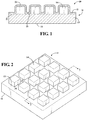
- a light emitting diode (LED) device 10 formed in accordance with the method of the present invention, includes an LED array 11 having a preformed lamination layer 12 (PL layer 12) conformally coated thereon.
- the PL layer 12 has become a conformed lamination layer in Figure 1 .
- the PL layer 12, and the related conformed lamination layer of the conformally coated article is constructed in a single layer form, as shown in Figures 1-6 .
- the related conformed lamination layer is constructed as a multi-layer laminate (not shown) and the method comprises fabricating a conformally coated article comprising the multi-layer laminate form of the conformed lamination layer and the object.
- the multi-layer laminate form of the conformed lamination layer may be constructed by any suitable method such as either (a) manufacturing the PL layer 12 as a multi-layer laminate, and using the multi-layer laminate form of PL layer 12 in the inventive method; or (b) using a single layer form of the PL layer 12 in the inventive method to give the single-layer laminate form of the conformed lamination layer, and then repeating the inventive method at least one time, with the same or different single layer form of the PL layer 12, to give a conformally coated article comprising, among other things, the multi-layer form of the conformed lamination layer.
- the LED array 11 includes a submount wafer 13 (an example of a substrate, which is an example of the object), having a first side 15 and a second side 16.
- the first side 15 of the submount wafer 13 has a perimeter portion 18 surrounding an inner portion 19.
- a submount wafer 13 is a type of substrate that comprises a plurality of light emitting diodes (LEDs) 14 arranged to enable fabrication of a plurality of laminated LEDs 14, which may then be singulated after lamination to give a plurality of individual laminated LEDs.
- the method employs the submount wafer as the substrate and further comprises singulating the conformally coated LED array to give a plurality of individual laminated LEDs.
- the LED array 11 also includes an array of LEDs 14 disposed on the inner portion 19 of the first side 15 of a submount wafer 13. Each individual LED 14 is spaced apart from the next adjacent LED 14 along the first side 15 of the inner portion 19.
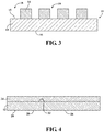
- Figures 1-3 illustrates one configuration of diodes 14 placed onto the inner portion 19 of the first side of the submount wafer
- the number, relative location, and spacing of the diodes 14 within the inner portion 19 can vary in terms of number, relative location, and/or spacing from that illustrated in Figures 1-3 .
- the size and shape of each of the individual diodes 14 defining the array of LEDs may be the same or different.
- the height of one diode 14 extending beyond the first side 15 of the submount wafer 13 may vary with respect to one or more of the additional diodes 14 in the array.
- the relative size of the diodes 14 to the size of the submount wafer 13 is also not limited by the illustrated configuration in Figures 2 and 3 .
- the shape of the submount wafer 13, as illustrated in Figure 1-3 as generally square along the first side 15, may vary in any number of ways.
- the shape may be circular, rectangular, regularly shaped, or irregularly shaped, depending upon its intended use.
- the size of the perimeter portion 18 relative to the inner portion 19 of the submount wafer 13 may also vary form the size illustrated in Figure 2 .
- the PL layer 12 includes a first surface 20 and a second surface 22 opposite the first surface 20.
- the PL layer 12 includes a middle portion 26 surrounded by an edge portion 28.
- the PL layer 12 may be a free-standing film.
- the PL layer 12 may be coupled to a support layer 24 for ease of handling.
- a support layer 24 Prior to being conformally coated to the LED array 11, a support layer 24 is typically coupled to one or both of the first surface 20 and second surface 22 (as shown in Figure 4 the support layer 24 is coupled to the second surface 22) of the PL layer 12 for easy handling.
- the support layer or layers 24, if present, are removed prior to heat softening the middle portion 26 of the PL layer 12, prior to forming the gastight seal and prior to conforming the PL layer 12 to the LED array 11 as described further below.
- the heat-softened middle portion 26 of the PL layer 12 is obtained by heating the middle portion 26 to the first temperature in a single heating step prior to the PL layer 12 being conformally coated over the LED array 11.
- the PL layer 12 generally shaped (sized or profiled) to correspond to the shape (size or profile) of the submount wafer 13 to which it is applied, wherein the middle portion 26 of the PL layer 12 generally corresponds in size and shape to the inner portion 19 of the submount wafer 13 and wherein the edge portion 28 generally corresponds in size and shape to the perimeter portion 18 of the submount wafer 13.
- the preformed lamination layer 12 typically includes a phosphor material, typically in powder form, disposed within a substantially uncured thermosetting material.
- the PL layer 12 is deformable (i.e., flexible at room temperature)
- substantially uncured refers to a thermosetting material has been prepared and kept at a temperature below about 30° C so as not to cure (i.e., crosslink) other than a minor amount of crosslinking that may occur during the mixing of the components and in storing the resultant material.
- Coatings of a slurry of the thermosetting material or silicone binder, with or without phosphor material, may be dried at about 70° C or less to give dried films thereof, and the dried films remain substantially uncured.
- the substantially uncured thermosetting material is a silicone binder.
- the PL layer 12 may be formed by mixing the phosphor material with the silicone binder to form a slurry and then applying the slurry to the support layer 24 and drying the slurry.
- the slurry may be formed with aid of a liquid vehicle such as an organic solvent such as toluene, butyl acetate, methyl ethyl ketone, dioxane, xylenes, or the like.
- the silicone binder or substantially uncured thermosetting material may be dispersed in the liquid vehicle to form a dispersion.
- the dispersion may have a nonvolatile content of 50 to 80 wt% (e.g., 65 wt%, 70 wt%, or 75 wt%).
- Phosphor particles may be mixed into the dispersion to form the slurry.
- the slurry may have a nonvolatile content of from > 50 to 90 wt% (e.g., 70 wt%, 80 wt%, or 85 wt%).
- Nonvolatile content refers to concentration of all constituents except the liquid vehicle.
- the PL layer 12 is conformally coated to the LED array 11, thereby becoming a conformed lamination layer.
- a conformal coating of the PL layer 12 to the LED array 11 is achieved wherein the first surface 20 of the middle portion 26 of the PL layer 12 is brought into sealing contact over each of the exposed portions of the diodes 14 and into contact with the first side 15 of the submount wafer 13 between each of the diodes 14 within the inner portion 19.
- the edge portion 28 of the PL layer 12 is brought into sealing contact over the perimeter portion 18 of the first side of the submount wafer 13.
- the PL layer 12 provides a protective and durable coating layer for the LEDs 14 of a consistent layer thickness that is substantially defect-free.
- the phosphor material contained within this conformed layer having uniform and consistent thickness allows light emitted from the diodes 14 individually and collective to be directed to provide a desired light effect.
- this invention is directed to vacuum lamination methods for forming electronic and optoelectronic devices such as semiconductor devices.
- the present invention is directed to vacuum lamination methods for forming these LED devices 10 as illustrated in Figure 1 , with exemplary methods described below with respect to the logic flow diagrams of Figures 7 and 8 below.
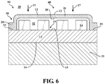
- the method for forming the LED devices 10 in accordance with the present invention includes the use of a fabrication device (shown as 50 in Figure 6 ) that includes a vacuum chamber (shown as 40 in Figure 6 ).
- Step 100 the method begins with Step 100, wherein the PL layer 12 is mounted over the LED array 11.
- the term "mounted”, as provided herein, refers to the placement of the PL layer 12 adjacent to the LED array 11, and is not intended to refer to or suggest that the PL layer 12 is fastened or otherwise secured to the array 11.
- the PL layer 12 is arranged wherein the first surface 20 of the PL layer 12 is located between the first side 15 of the submount wafer 13 and the second surface 22, and wherein the first side 15 of the submount wafer 13 is located between the first surface 20 and the second side 16.
- the middle portion 26 of the PL layer 12 is adjacent to the inner portion 19 of the array 11, and therefore adjacent to the corresponding array of diodes 14, while the edge portion 28 is adjacent to the perimeter portion 18.
- the mounting of the PL layer 12 to the LED array 11 of Step 100 is performed within the vacuum chamber 40, whereas in other embodiments the mounting of the PL layer 12 to the LED array 11 of Step 100 is performed prior to placing the PL layer 12 and LED array 11 into the vacuum chamber 40.
- Step 110 as shown in Figure 5 , a portion 29 of the edge portion 28 of the PL layer 12 is adhered to the perimeter portion 18 of the first side 15 of the submount wafer 13. This may alternatively be referred to as tacking, or spot-tacking, the portion 29 of the edge portion to the perimeter portion 18. In this arrangement, another portion 30 of the edge portion 28 is not adhered to the perimeter portion 18. As such, in Step 110, a gastight seal is not created along between the edge portion 28 and the perimeter portion 18. See also Figure 10 .
- portion 29 is heated to a first temperature to soften the portion 29 (i.e., to make the portion 29 flowable).
- the middle portion 26 and the portion 30 of the PL layer 12 are maintained a temperature below the first temperature (i.e., the middle portion 26 and the portion 30 are not softened or otherwise made flowable).
- portion 29 is heated by pressing on the support layer 24 at a location opposite portion 29 while not pressing on the support layer 24 at a location opposite portion 30 such that portion 29 of the edge portion 28 of the PL layer 12 is adhered to the perimeter portion 18 of the first side 15 of the submount wafer 13, while portion 30 of the PL layer 12 is not adhered to the perimeter portion 18 of the first side 15 of the submount wafer 13.
- the substantially uncured thermosetting material of the portion 29 of the PL layer 12 begins to react (i.e., begins to crosslink and cure), therein reducing the flow properties of the portion 29 over time as the degree of crosslinking increases.
- the portion 29 of the PL layer 12 becomes highly flowable upon reaching the first temperature, and then subsequently becomes less flowable as the degree of crosslinking within the portion 29 of the PL layer 12 increases.
- the first temperature is dependent upon the rheological properties and the curing properties (i.e., crosslinking) of the composition of the uncured thermosetting material used in the PL layer 12.
- the first temperature also cannot exceed the temperature wherein the chemical or physical properties of the submount wafer 13 or diodes 14 are negatively impacted.
- the uncured thermosetting materials include a silicone binder, as described above
- the first temperature is generally in the range of 110°-170° C, alternatively 110° to 150° C, alternatively 120° to 140° C, alternatively 150°-170° C, alternatively a temperature used in the examples later, to achieve flow and begin the crosslinking process, although the first temperature may be higher or lower depending upon the particular chemistry of the material used.
- a heater device (shown as 39 in Figure 6 ) that is positioned to be in thermal communication with the portion 29 of the PL layer 12.
- the term "thermal communication”, as referred to herein, describes wherein the heater device 39, when activated, is able to increase the temperature of the portion of the PL layer 12 to which it is directed.
- the heater device 39 may be a device that is capable of radiating heat to a desired portion of the PL layer 12 (wherein the device is either brought into contact with, or closely coupled to, the PL layer 12) to raise the temperature of the PL layer 12 to the first temperature.
- the heater device 39 may be a hot plate positioned to directly contact or be closely coupled to a desired location on the PL layer 12.
- the heater device 39 may be an infrared light emitting lamp or laser.
- the heater device 39 may be able to heat the PL layer 12 by methods other than by radiating heat.
- the heater device 39 may be a laser, alternatively an infrared lamp, which directs electromagnetic radiation to a desired portion of the PL layer 12.
- the heater device 39 is positioned within a portion of the vacuum chamber 40 such that it may be directed to the portion 29 of the PL layer 12.
- the softened portion 29 heated to the first temperature is pressed to the perimeter portion until adhesion is obtained between the first surface 20 of the softened portion 29 and the perimeter portion 18, and wherein adhesion is not obtained between the another portion 30 and the perimeter portion 18.
- the pressing may be done by applying pressure to the second surface 22 manually, through the use of a mechanical device, or by any other means that can create sufficient force to obtain adhesion between the softened portion 29 and the perimeter portion 18.
- the heating and pressing steps are done simultaneously, while in other embodiments the portion 29 may first be heated to the first temperature prior to being pressed onto the perimeter portion 18
- Step 110 may be performed wherein a vacuum has been applied within the vacuum chamber 40.
- Step 110 further includes removing (not shown in Figure 7 ) the support layer 24 from the second surface 22 prior to Step 120 below.
- the support layer 24 is removed from the second surface 20 by applying a pressure sensitive adhesive (PSA) tape to the support layer 24 to adhere it to the support layer 24 and pulling the PSA tape and adhered support layer 24 away from the second surface 20.
- PSA pressure sensitive adhesive
- Other technigues may be used to remove the support layer 24 from the second surface 20 such as using forceps or a knife blade to apply a mechanical force to the support layer 24 so as to separate it from the second surface 20.
- Figure 5A is a cross-sectional view of the PL layer 12 coupled over the LED array 11 after removal of the support layer 24 (not shown) in which a portion 29 of the edge portion 28 of the PL layer 12 is adhered to the perimeter portion 18 of the submount wafer 13 and another portion 30 of the edge portion 28 of the PL layer 12 is not adhered to the perimeter portion 18 of the submount wafer 13.
- Step 115 in certain embodiments, wherein Step 110 is not performed in the vacuum chamber 40, the LED array 11 of a submount wafer 13 having the portion 29 adhered to the perimeter portion 18 is placed into the vacuum chamber 40 of the fabrication device 50.
- Step 110 is performed in the vacuum chamber 40, the logic proceeds to Step 120.
- Step 120 a vacuum is applied within the vacuum chamber 40, and the PL layer 12, including both the edge portion 28 (and specifically portion 30 of the edge portion 28) and the middle portion 26, are heated to the first temperature to soften the middle portion 26 and portion 30 (i.e., make them flowable).
- the heat-softened middle portion 26 is obtained by heating the middle portion 26 of the PL layer 12 to the first temperature in a single heating step prior to the PL layer 12 being conformally coated over the LED array 11. Any support layer 24 has been removed before proceeding with step 120.
- the heating may occur after the vacuum is completely applied. Alternatively, the heating may occur simultaneously with applying the vacuum as long as the vacuum chamber is evacuated before the middle portion 26 and edge portion 28 (specifically portion 30 of the edge portion 28).
- a heater device 39 that is the same or different from the heater device 39 described above in Step 110, may be used to heat the preformed layer 12 to the first temperature.
- the heater device 39 is a heater device 39, such as a hot plate, that is positioned within the vacuum chamber 40 and in a position adjacent to, but not in thermal communication with, the second side 16 of the LED array 11 (i.e., wherein the second side 16 is positioned between the heater device 39 and the first side 15 of the LED array 11 and wherein the heater device 39 does not raise the temperature of the LED array 11 and mounted layer 12 even if activated).
- the LED array 11 is moved from a first position not in thermal communication with the heater device 39 to a second position in thermal communication device (i.e., the second side 16 of the LED array 11 is moved closer to or in contact with the heater device 39). In this second position, when the heater device 39 is activated, heat is transferred to the LED array and to the mounted layer 12 to heat the middle portion 26 and portion 30 to the first temperature to soften the middle portion 26 and portion 30 of the PL layer 12, as described above.
- the vacuum chamber 40 includes an external frame having at least one displaceable structure that is moveable between an engaged position and a disengaged position.
- the engaged position corresponding to the first position described in the previous paragraph
- the second side 16 of the LED array 11 is disposed on the at least one displaceable structure such that it is suspended adjacent to the heater device 39, wherein the LED array 11 is therefore not in thermal communication with the heater device 39.
- the LED array 11 When the at least one displaceable structure is moved from the engaged position to the disengaged position, the LED array 11 is no longer in contact at least one displaceable structure, therein allowing the LED array 11 to move into thermal communication with the heater device 39 ( i.e., move to the second position), which therefore allows the LED array and film to be heated when the heater portion is activated.
- the displaceable structure is a push pin or spring which can extend externally from the external frame in the engaged position and recede into the frame in the disengaged position.
- Step 130 the softened edge portion 28 is sealed to the perimeter portion 18 under the applied vacuum, thereby creating a sealed perimeter 33 between the edge portion 28 and the perimeter portion 18.
- the substantially uncured thermosetting material of the portion 30 of the PL layer 12 begins to react (i.e., crosslink or cure), therein reducing the flow properties of the portion 30 as the degree of crosslinking increases.
- a gastight inner region 32 is created, which is defined within the space between the softened middle portion 26, the first side 15 of the submount wafer 13 and the sealed perimeter 33.
- gas flow is prevented from moving from the gastight portion 32, through the sealed perimeter 33, and to the remainder of the vacuum chamber 40, otherwise referred to as area (shown as 35 in Figure 6 ) of vacuum chamber 40, and vice versa.
- Step 140 after the sealed perimeter 33 is created, the entire lamination layer 12 is conformed over the LED array 11. This is accomplished by raising the gas pressure within the area 35 of the vacuum chamber 40 relative to the gas pressure in the gastight inner region 32.
- the gas pressure may be raised within the area 35 by breaking the applied vacuum in the vacuum chamber 40 and allowing a gas to enter the vacuum chamber 40.
- the breaking the applied vacuum and allowing a gas to enter the vacuum chamber 40 may comprise venting or opening the vacuum chamber 40 to an environmental atmosphere (e.g., air) and/or (affirmatively) introducing a gas into the vacuum chamber 40 (e.g., from a source of compressed gas).
- the gas pressure in the vacuum chamber may be raised to a pressure greater than the reduced gas pressure in the gastight inner region 32 sufficient to achieve the conformal coating step, such as to a pressure from greater than the reduced gas pressure to a pressure less than ambient pressure (e.g., ⁇ 101 kilopascals (kPa)), to ambient pressure (about 101 kPa), or to a pressure greater than ambient pressure, e.g., up to 200 kPa.
- ambient pressure e.g., ⁇ 101 kilopascals (kPa)
- ambient pressure about 101 kPa
- ambient pressure e.g., up to 200 kPa.
- the increased pressure in area 35 therefore exerts force on the second surface 22 of the softened PL layer 12 (shown by arrow 37 in Figure 6 ), therein pushing the first surface 20 into sealing (i.e., conformal) contact with each of the features present on the first side 15 of the LED array 11, including over each of the array of diodes 14, over the inner portion 19 of the first side 15 of the wafer submount 13 between the diodes 14, and over first side of the perimeter portion 18 of the wafer submount 13.
- sealing i.e., conformal
- the substantially uncured thermosetting material of the middle portion 26 and portion 30 of the PL layer 12 continues to react and cure. Over time, the entire layer 12 forms a cured and conformed layer 12 over the entire first surface 15 of the LED array 11.
- the gas pressure increase of Step 140 is created by removing the vacuum from the vacuum chamber 40 (i.e. venting the vacuum chamber 40), thereby increasing the gas pressure within the vacuum chamber 40 in area 35. Still further, in other embodiments, the gas pressure in area 35 may alternatively or further be increased in Step 140 by introducing additional gas into the area 35 of the vacuum chamber 40.
- the gas pressure may be raised to ambient pressure, alternatively to a pressure greater than 101 kPa, e.g., up to 200 kPa.
- the present invention also provides an alternative lamination method than the embodiment provided in Figure 7 .
- this method as described in conjunction with the logic flow diagram illustrated in Figure 8 , the entire edge portion 28 of the PL layer 12 is sealed to the perimeter 18 portion in a single step, as opposed to first tacking (or adhering) a portion 29 of the edge portion 28 in a first step (Step 110 above) and then subsequently sealing the entire edge portion 28 to the perimeter portion 18 (Step 130 above) as described in conjunction with the logic flow diagram of Figure 7 .
- Step 200 the lamination method begins with Step 200, wherein the PL layer 12 is mounted over the LED array 11.
- the method of Step 200 is substantially as provided above with respect to Step 100 of Figure 7 and not repeated herein.
- the mounting of the PL layer 12 to the LED array 11 of Step 200 is performed within the vacuum chamber 40, whereas in other embodiments the mounting of the PL layer 12 to the LED array 11 of Step 200 is performed prior to placing the PL layer 12 and LED array 11 into the vacuum chamber 40.
- Step 210 in certain embodiments, wherein Step 200 is not performed in the vacuum chamber 40, the LED array 11 having the mounted PL layer 12 is placed into the vacuum chamber 40 of the fabrication device 50.
- Step 200 is performed in the vacuum chamber 40, the logic proceeds to Step 120. Any support layer (e.g., 24) has been removed before proceeding with step 220.
- Step 220 a vacuum is applied within the vacuum chamber 40, and the edge portion 28 of the PL layer 12 is heated to the first temperature to soften the edge portion 28 ( i.e., make them flowable).
- Step 230 the softened edge portion 28 is sealed to the perimeter portion 18 under the applied vacuum, thereby creating a sealed perimeter 33 between the edge portion 28 and the perimeter portion 18.
- the substantially uncured thermosetting material of the edge portion 28 of the PL layer 12 begins to react (i.e., crosslink or cure), therein reducing the flow properties of the edge portion 28 as the degree of crosslinking increases.
- a gastight inner region 32 is created, which is defined within the space between the middle portion 26, the first side 15 of the submount wafer 13 and the sealed perimeter 33. In other words, gas flow is prevented from moving from the gastight portion 32, through the sealed perimeter 33, and to the remainder 35 of the vacuum chamber 40, and vice versa.
- Step 230 further includes removing the support layer 24 from the second surface 22 prior to Step 240 below.
- the support layer 24 may be removed prior to beginning sealing (before Step 230).
- the support layer 24 is removed from the second surface 20 by applying a pressure sensitive adhesive (PSA) tape to the support layer 24 to adhere it to the support layer 24 and pulling the PSA tape and adhered support layer 24 away from the second surface 20.
- PSA pressure sensitive adhesive
- Step 240 while still under vacuum, the PL layer 12, including both the edge portion 28 and the middle portion 26, are heated to the first temperature to soften the middle portion 26 (i.e., make the middle portion flowable).
- the heat-softened middle portion 26 is obtained by heating the middle portion 26 of the PL layer 12 to the first temperature in a single heating step prior to the PL layer 12 being conformally coated over the LED array 11.
- a heater device 39 that is the same or different from the heater device 39 described above in anyone of Steps 110, Step 230, may be used to heat the preformed layer 12 to the first temperature.
- the heater device 39 is a heater device 39, such as a hot plate, that is positioned within the vacuum chamber 40 and in a position adjacent to, but not in thermal communication with, the second side 16 of the LED array 11 (i.e., wherein the second side 16 is positioned between the heater device 39 and the first side 15 of the LED array 11 and wherein the heater device 39 does not raise the temperature of the LED array 11 and mounted layer 12 even if activated).
- the LED array 11 is moved from a first position not in thermal communication with the heater device 39 to a second position in thermal communication device (i.e., the second side 16 of the LED array 11 is moved closer to or in contact with the heater device 39). In this second position, when the heater device 39 is activated, heat is transferred to the LED array and to the mounted layer 12 to heat the middle portion 26 and portion 30 to the first temperature to soften the middle portion 26 and portion 30 of the PL layer 12, as described above.
- the vacuum chamber 40 includes an external frame having at least one displaceable structure that is moveable between an engaged position and a disengaged position.
- the engaged position corresponding to the first position described in the previous paragraph
- the second side 16 of the LED array 11 is disposed on the at least one displaceable structure such that it is suspended adjacent to the heater device 39, wherein the LED array 11 is therefore not in thermal communication with the heater device 39.
- the LED array 11 When the at least one displaceable structure is moved from the engaged position to the disengaged position, the LED array 11 is no longer in contact at least one displaceable structure, therein allowing the LED array 11 to move into thermal communication with the heater device 39 ( i.e., move to the second position), which therefore allows the LED array and film to be heated when the heater portion is activated.
- the displaceable structure may be moved so as to impinge on the edge portion 28 of the lamination layer 12 on to the perimeter portion 18 of the submount wafer 13, thereby forcing gastight sealing around the perimeter.
- the displaceable structure is a push pin or spring which can extend from the external frame in the engaged position and recede into the frame in the disengaged position.
- Step 250 after the middle portion 26 of the lamination layer 12 is heated to the first temperature, the entire lamination layer 12 is conformed over the LED array 11. This is accomplished by raising the gas pressure within the vacuum chamber 40 in area 35 relative to the gastight inner region 32, as described above in Step 140 of Figure 7 .
- the increased pressure in area 35 therefore exerts force on the second surface 22 of the softened PL layer 12, as shown by arrow 37 in Figure 6 , therein pushing the first surface 20 into sealing (i.e., conformal) contact with each of the features present on the first side 15 of the LED array 11, including over each of the array of diodes 14, over the inner portion 19 of the first side 15 of the wafer submount 13 between the diodes 14, and over first side of the perimeter portion 18 of the wafer submount 13.
- sealing i.e., conformal
- the substantially uncured thermosetting material of the middle portion 26 continues to react and cure. Over time, the entire layer 12 forms a cured and conformed layer over the entire first surface 15 of the LED array 11.
- the gas pressure increase of Step 250 is created by removing the vacuum from the vacuum chamber 40 (i.e. venting the vacuum chamber 40), thereby increasing the gas pressure within area 35 relative to the gastight inner region 32. Still further, in other embodiments, the gas pressure may be increased in Step 250 by introducing additional gas into area 35 of the vacuum chamber 40.
- the resultant LED device 10 as illustrated and described with respect to Figure 1 above, as formed according to the method of the logic flow diagram associated with either Figure 7 or 8 , may then be removed from the vacuum chamber 40 of the fabrication device 50 and is available for use in a wide variety of lighting applications.
- the LED device 10 formed by the method of the present invention includes conformally coated PL layer 12 that provides a protective and durable coating layer for the LEDs 14 of a consistent layer thickness that is substantially defect-free.
- the PL layer 12 is shown as a conformed lamination layer.
- the phosphor material contained within this conformed layer 12, uniformly and consistently distributed within the conformed film layer 12, allows light emitted from the individual diodes 14, or collective from two or more of the array of diodes, to be directed or otherwise filtered to provide a desired light effect for its intended use.
- the vacuum lamination methods of the present invention offer numerous advantages over two-step vacuum lamination methods utilizing two distinct heating steps.
- the processing window for applying and conforming the preformed lamination layer (e.g., 12) is increased relative to the two-step vacuum lamination techniques in the prior art in which two distinct heating steps are utilized.
- This increased processing window allows for the use of preformed lamination layers (e.g., 12) having different phosphor levels, in combination with additional or differing binder compositions having varying rheologies or cure speeds, which may need longer heating times than two-step vacuum lamination techniques allow.
- Resulting LED devices e.g., 10) may therefore be formed having a wider variety of colors and quality of light than may be realized in LED devices formed with two-step vacuum lamination techniques.
- the increased processing time allows for the PL layer 12 to be conformed over an array of diodes 14 having different feature heights (such as, for example, an array of diodes 14 including shorter conventional diodes and taller sapphire diodes) while still achieving uniform thickness of the phosphor layer on the highest height LEDs.
- the desired lighting characteristics for these array of diodes can be precisely and predictably controlled.
- the PL layer 12 is shown not touching the tops of diodes 14. This configuration may occur when LED array has additional structures (not shown) that may be taller than diodes 14 and therefore may hold the PL layer 12 off of the diodes 14 prior to conformal coating step. Alternatively, if there are no additional structures that are taller than diodes 14, the PL layer 12 may be allowed to rest on and touch the tops (not indicated) of diodes 14.
- Figure 9 is a graphical plot of a process coordinate of an embodiment of a method of forming the conformally coated article from the assembly comprising the preformed lamination layer and the object having a first surface in need of lamination and a second surface opposite the first surface.
- the process coordinate is divided into three general successive stages 1, 2 and 3, starting with the assembly at the beginning of stage 1 (far left) and ending with the conformally coated article at the end of stage 3 (far right).
- the process coordinate plots temperature (solid line) of the preformed lamination layer and pressure (dashed line) within the vacuum chamber of the fabrication device.
- stage 1 which independently comprises embodiments of the Apply Vacuum portion of Step 120 of Fig. 7 (and may not comprise the And Heat Middle Portion of Step 120) and comprises Step 220 of Fig. 8 , the assembly is spaced apart from an activated heater (not shown) and the vacuum chamber is evacuated via the applied vacuum to remove gas from the vacuum chamber and from between the preformed lamination layer and the object.
- the process coordinate shows a substantial decrease in pressure within the vacuum chamber and at most a slight increase in the temperature of the preformed lamination layer of the assembly, wherein any temperature increase stage 1 is insignificant relative to the time it takes to evacuate the vacuum chamber and relative to the temperature needed for softening or curing the preformed lamination layer.
- Stage 1 includes the applying a vacuum step, which occurs prior to the heating step.
- the applying a vacuum within the vacuum chamber removes gas from the vacuum chamber, including from between the first surface of the preformed lamination layer and the first surface of the object, so as to create the applied vacuum in the vacuum chamber of the fabrication device.
- stage 2 which independently comprises embodiments of Step 130 of Fig. 7 and Steps 230 and 240 of Fig. 8 , the vacuum chamber and the space between the first surface of the preformed lamination layer and the first surface of the object are under the applied vacuum.
- the assembly is moved toward the activated heater (or vice versa) until the second surface of the object is brought into thermal communication with the activated heater.
- the thermal communication results in a rapid increase in temperature of the object, and in turn a rapid increase in the temperature of the preformed lamination layer in contact therewith.
- the heat-softened middle portion of the preformed lamination layer is obtained by heating the middle portion to the first temperature in a single heating step prior to the preformed lamination layer being conformally coated over the object.
- the temperature of the edge portion and middle portion of the preformed lamination layer has reached a first temperature wherein the edge and middle portions of the preformed lamination layer soften and the edge portion seals to the perimeter portion of the first surface of the object, thereby forming the gastight seal under the applied vacuum and such that the assembly contains the gastight inner region.
- the gastight inner region contains the reduced gas pressure, which is effectively equal to the applied vacuum in the vacuum chamber.
- stage 2 includes the heating and sealing steps, but not the conforming step.
- stage 3 which independently comprises embodiments of Step 140 of Fig. 7 and Step 250 of Fig. 8 , heating is maintained such that temperature of the preformed lamination layer is maintained at or above its softening temperature while gas pressure within the vacuum chamber is increased.
- the gas pressure within the vacuum chamber becomes greater than the reduced gas pressure within the gastight inner region.
- stage 3 is the conforming step and occurs after the heating and sealing steps.
- the first lamination temperature, duration of evacuation during the applied vacuum step, and timing of the applying a vacuum step relative to a heating step may depend on a number of factors that would be within the ordinary skill in the art to control. Such factors include pump rate of the fabrication device (i.e., how quickly a vacuum chamber of a given fabrication device may be evacuated), the vacuum chamber's thermal characteristics (i.e., its temperature and heat conduction ability), viscoelastic properties of the preformed lamination layer, and design and nature of the object being laminated (e.g., how small are the surface features on the inner portion of the first surface of the object, and thus how easily those surface features are conformally coated and how critical is achieving a quality conformal coating is for the use of the conformally coated article).
- pump rate of the fabrication device i.e., how quickly a vacuum chamber of a given fabrication device may be evacuated
- the vacuum chamber's thermal characteristics i.e., its temperature and heat conduction ability
- viscoelastic properties of the preformed lamination layer
- the first temperature of the preformed lamination layer may be sufficiently high to soften the preformed lamination layer and to allow formation and maintenance of the gastight seal, while not too high to cause premature sealing prior to achieving an extent of removing of gas from between the preformed lamination layer and the object in order to avoid entrapping air or other gas under the preformed lamination layer. If the preformed lamination layer is composed of a material that generates volatiles upon heating to high temperature, the first temperature of the preformed lamination layer may be kept below the volatilization temperature.
- the rate of evacuation may be adjusted to be sufficiently faster than the rate of heating of the preformed lamination layer such that timing of achieving a satisfactory applied vacuum in the vacuum chamber is achieved before the preformed lamination layer begins to soften and trap air or other gas.
- the preformed lamination layer may begin to be heated before the applied vacuum is achieved, but the rate of evacuation is controlled such that any heating of the preformed lamination layer prior to achieving full applied vacuum is insufficient to soften the same.
- the heating of the edge portion of the preformed lamination layer is begun soon after the applied vacuum is achieved and is sufficiently rapid to enable forming of the gastight seal soon after (e.g., less than 5 minutes after) heating is begun.
- the heating of the edge portion of the preformed lamination layer is begun before the applied vacuum is achieved but the rate of heating is sufficiently slow relative to the rate of evacuating the vacuum chamber such that the edge portion of the preformed lamination layer does not reach the first temperature or soften until after the applied vacuum is achieved.
- Figure 10 is a top view of an assembly 8 prepared by an embodiment of the method, wherein the assembly 8 is produced by an adhering step but before a gastight sealing step.
- the PL layer 12 is mounted over an array 11 of diodes 14, and middle portion 26 of the PL layer 12 is not conformally coating diodes 14.
- the edge portion 28 of the PL layer 12 is spot adhered at one or more locations 29 to the perimeter portion 18 of submount wafer 13 and not adhered at one or more locations 30 to perimeter portion 18 of submount wafer 13.
- the assembly 8 is ready for the applying vacuum step or the introducing step and applying vacuum step, etc.
- inventive embodiments are any one of the following numbered aspects 1 to 33.
- inventive aspects are any one of the following numbered aspects.
- the silicone is a macromolecule or a collection of macromolecules of a resin-linear organosiloxane.
- Resin-linear polyorganosiloxane macromolecules may be hydrosilylation cured resin-linear organosiloxane block copolymers (R-LOB Copolymers).
- R-LOB Copolymers have a different monomer arrangement than those of non-block copolymers such as statistical, random or alternating copolymers.
- R-LOB Copolymers may be diblock, triblock, or higher block copolymers.
- R-LOB Copolymers are composed of macromolecules that are characterized by distinct linear blocks and distinct resin blocks.
- the linear blocks typically contain mostly, substantially all, or all D-type organosiloxane units, which are primarily bonded together to form bivalent straight chain polymeric segments (e.g., having from 10 to 400 units each), which bivalent straight chain polymeric segments are referred to herein as "linear blocks.”
- the resin blocks contain a majority, substantially all, or all of T-type organosiloxane units or Q units, although typically they are T-type organosiloxane units.
- Q units SiO 4/2
- the R-LOB Copolymers may contain a relatively small number* of M-type organosiloxane units (R 3 SiO 1/2 ), wherein R is hydrocarbyl; *typically less than 5 mol% M-type units.)
- the T-type organosiloxane units are primarily bonded to each other to form polyvalent branched chain polymeric segments, which are referred to herein as "non-linear blocks.”
- the R-LOB Copolymers are composed of macromolecules wherein the linear blocks are bonded to the non-linear blocks. In solid forms of the R-LOB Copolymer, a significant number of these non-linear blocks may aggregate together to form nano-domains.
- the aggregated non-linear blocks of the R-LOB Copolymers may be referred to as hard domains and the linear blocks as soft domains.
- the R-LOB Copolymers may be characterized by higher glass transition temperatures (Tg) than those of non-block copolymers.
- Tg glass transition temperatures
- These R-LOB Copolymers may be designed to contain a low molar amount of unsaturated aliphatic groups, which enable cross-linking of the copolymers in downstream industrial applications such as sealing or encapsulating (opto)electronic devices.
- Some embodiments of these R-LOB Copolymers further contain an additional type of reactive group, which enables the R-LOB Copolymers so functionalized to be used in dual-cure mechanisms.
- Some R-LOB Copolymers are of the nanophase-separated type, which comprise nano-sized domains of linear blocks predominantly comprised of D units and of resin blocks predominantly comprised of T units.
- Resin-linear polyorganosiloxane macromolecules may comprise a hydrosilylation-cured resin-linear organosiloxane block copolymer comprising: 40 to 90 mole percent D-type units of the formula [R 1 2 SiO 2/2 ], 10 to 60 mole percent T-type units of the formula [R 2 SiO 3/2 ], 0.5 to 35 mole percent silanol groups [Si-OH]; wherein each R 1 and R 2 independently is a (C 1 -C 30 )hydrocarbyl that has 0 aliphatic unsaturated bond or a (C 1 -C 30 )hydrocarbyl which comprises at least 1 aliphatic unsaturated bond, wherein the resin-linear organosiloxane block copolymer comprises from 0.5 to 5 mole percent of the (C 1 -C 30 )hydrocarbyl comprising at least one aliphatic unsaturated bond; wherein the D-type units [R 1 2 SiO 2/2 ] are
- Any resin-linear organosiloxane block copolymer is contemplated, including R-LOB Copolymers that are known in the art. E.g., see US 2014/0357827 A1 ; US 2013/0165602 A1 ; US 2013/0168727 A1 ; US 2013/171354 A1 ; US 2013/0172496 A1 , which issued as US 8,921,495 B2 ; and US 2013/0245187 A1 .
- Lamination Yield Test Method in a conformally coated LED array containing x total number of LED diodes and thus x gaps between each pair of electrodes, the gaps are visually inspected to determine the number, f, of gaps that are completely filled with the conformal coating and the number, u, of gaps that are unfilled or have air pockets.
- Examples 1a to 1e preparations of conformally coated LED arrays (1a) to (1e) using vacuum laminator (1).
- an LED array (1) was conformally coated with a preformed lamination layer (1) using vacuum laminator (1) as follows.
- the hot plate in vacuum laminator (1) was activated such that the temperature of the hot plate was allowed to reach a set point (see Table 1 below).
- on LED array (1) was placed preformed lamination layer (1) to give an assembly, and the assembly was placed in a carrier tray. After the temperature of the hot plate reached its set point, the loaded carrier tray was placed on the springs in vacuum laminator (1) such that the bottom of the carrier tray was about 0.3 cm above the activated hot plate.
- the resulting loaded vacuum laminator (1) was closed, and a vacuum applied for 1 minute to evacuate the vacuum chamber and create an applied vacuum therein, all while the springs held the loaded carrier tray above the hot plate, thereby minimizing heating of the submount wafer of LED array (1), and in turn preformed lamination layer (1). Then, without contacting preformed lamination layer (1), the bladder of vacuum laminator (1) was lowered to push the loaded carrier tray onto the hot plate, where it remained under vacuum for an initial heating time of 1 minute and 30 seconds. This allowed the hot plate to heat the submount wafer, which in turn heated preformed lamination layer (1).
- Examples 1f to 1j preparations of conformally coated LED arrays (1f) to (1j) using vacuum laminator (2).
- Replicate Examples 1a to 1e except use vacuum laminator (2) instead of vacuum laminator (1) and place the loaded carrier tray directly on the hot plate instead of on the support springs of vacuum laminator (1) to give a different one of conformally coated LED arrays (1f) to (1j), respectively, which were then removed from the vacuum chamber.
- Table 2 below shows the lamination yield at various hot plate temperature set points ranging from 110° to 150° C.
- Table 2 conformally coated LED arrays (1a) to (1e) prepared using vacuum laminator (2).
- Examples 2a to 2e preparations of conformally coated LED arrays (2a) to (2e) using vacuum laminator (1): Replicate the procedure of Examples 1a to 1e except use preformed lamination layer (2) instead of preformed lamination layer (1) to give conformally coated LED arrays (2a) to (2e).
- Table 3 shows the lamination yield at various hot plate temperature set points ranging from 110° to 150° C.
- Table 3 conformally coated LED arrays (2a) to (2e) prepared using vacuum laminator (1).
- Example 2a As shown by the lamination yield data in Table 3, specifically for Example 2a relative to Examples 2b to 2e, if the hot plate set point temperature is too low, preformed lamination layer (2) does not soften sufficiently after only the 1 minute and 30 seconds and additional 2 minutes of heating time. Thus, the heating time may be increased if a set point temperature is otherwise too low in order to give the preformed lamination layer time to form the conformally coated article.
- the conditions in Example 2a may be improved so as to produce a conformal coating at a set point temperature of 110° C. In some embodiments Example 2a is excluded from this invention.
- Examples 2f to 2j preparations of conformally coated LED arrays (2f) to (2j) using vacuum laminator (2). Replicate Examples 1f to 1j except use preformed lamination layer (2) instead of preformed lamination layer (1) to give conformally coated LED arrays (2f) to (2j), respectively, which were then removed from the vacuum chamber. Table 4 below shows the lamination yield at various hot plate temperature set points ranging from 110° to 150° C. Table 4: conformally coated LED arrays (1a) to (1e) prepared using vacuum laminator (2).
- the rate of evacuation may be increased or the set point temperature may be decreased if a set point temperature is otherwise too high in order to give evacuation step time to remove air from between the preformed lamination layer (2) and LED arrays 2 in order to form the conformally coated article.
- the conditions in Example 2f and 2h to 2j may be improved so as to produce a conformal coating at a set point temperature of 110°, 130°, 140°, or 150° C. In some embodiments Examples 2f and 2h to 2j are excluded from this invention.
- Example 3 preparation of conformally coated LED array (3) using vacuum laminator (1): Replicate the procedure of Example 1d (140° C) except use preformed lamination layer (3) instead of preformed lamination layer (1) to give conformally coated LED array (3). The lamination yield was 100%. Compare with Comparative Example 1 described above.
- Examples 4a preparation of conformally coated LED array (4) using vacuum laminator (1): Replicate the procedure of Example 1d (140° C) except use preformed lamination layer (4) instead of preformed lamination layer (1) and use a perimeter stamping jig configured to contact the entire edge portion of the second surface of the preformed lamination layer (4) and press same against the perimeter portion of the first side of the submount wafer while maintaining a gap between the edge portion of the first surface of the preformed lamination layer (4) and the perimeter portion of the first side of the submount wafer of LED array (1) so that the pressing does not tear the softened preformed lamination layer; use an initial heating time (after contact with hot plate but prior to vacuum release) of 15 seconds instead of 1 minute and 30 seconds; and use an additional heating time (after vacuum release) of 15 seconds instead of 2 minutes to give conformally coated LED array (4a).
- Example 1d 140° C
- a perimeter stamping jig configured to contact the entire edge portion of the second surface of the preformed lamination layer (4) and press same against the perimeter
- Total process time of 1.5 minutes evacuation time 1 minute and total heating time of 30 seconds.
- the stamping jig is used to press or impinge the edge portion of the preformed lamination layer on to the perimeter portion of the submount wafer, thereby forcing gastight sealing around the perimeter.
- the lamination yield was 100%. Compare with Comparative Example 2 described above.
- the perimeter jig facilitates sealing of the heat-softened edge portion of the preformed lamination layer to the perimeter portion of the first surface of the object.
- Examples 5a to 5e preparations of conformally coated LED arrays (5a) to (5e) using vacuum laminator (1).
- an LED array (1) is conformally coated with a preformed lamination layer (5) using vacuum laminator (1) as follows.
- the hot plate in vacuum laminator (1) is activated such that the temperature of the hot plate is allowed to reach a set point of 110°, 120°, 130°, 140° or 150° C, respectively.
- preformed lamination layer (5) is placed preformed lamination layer (5) to give an assembly, and the assembly is placed in a carrier tray.
- the loaded carrier tray is placed on the springs in vacuum laminator (1) such that the bottom of the carrier tray is about 0.3 cm above the activated hot plate.
- the resulting loaded vacuum laminator (1) is closed, and a vacuum is applied for 1 minute to evacuate the vacuum chamber and create an applied vacuum therein, all while the springs hold the loaded carrier tray above the hot plate, thereby minimizing heating of the submount wafer of LED array (1), and in turn preformed lamination layer (5).
- the bladder of vacuum laminator (1) is lowered to push the loaded carrier tray onto the hot plate, where it remains under vacuum for an initial heating time of 1 minute and 30 seconds.
- Examples 6a to 6e (prophetic): Replicate Examples 5a to 5e except use preformed lamination layer (6) instead of preformed lamination layer (5) to give conformally coated LED arrays (6a) to (6e). Determine the lamination yield of conformally coated LED arrays (6a) to (6e).
- Examples 7a to 7e (prophetic): Replicate Examples 5a to 5e except use Object (2) instead of LED array (1) (Object (1)) to give conformally coated glass sheets (7a) to (7e), respectively.
Landscapes
- Physics & Mathematics (AREA)
- Fluid Mechanics (AREA)
- Life Sciences & Earth Sciences (AREA)
- Engineering & Computer Science (AREA)
- Wood Science & Technology (AREA)
- Encapsulation Of And Coatings For Semiconductor Or Solid State Devices (AREA)
- Led Device Packages (AREA)
- Optical Filters (AREA)
- Blow-Moulding Or Thermoforming Of Plastics Or The Like (AREA)
- Structures Or Materials For Encapsulating Or Coating Semiconductor Devices Or Solid State Devices (AREA)
Claims (13)
- Un procédé de fabrication d'un article revêtu de façon conforme à partir d'un ensemble qui est logé dans une chambre à vide d'un dispositif de fabrication ;
dans lequel la chambre à vide contient un vide appliqué ;
dans lequel l'ensemble comprend une couche de stratification préformée et un objet ayant une surface nécessitant une stratification ;
dans lequel la couche de stratification préformée a une première surface et une deuxième surface à l'opposé de la première surface, et une portion de milieu ramollie à la chaleur à une première température et entourée par une portion de bord ;
dans lequel l'objet a une première surface et une deuxième surface à l'opposé de la première surface, et la première surface nécessitant une stratification et comprenant une portion interne et une portion de contour entourant la portion interne ;
dans lequel l'ensemble est configuré de telle sorte que la première surface de la couche de stratification préformée est positionnée en face de la première surface de l'objet, dans lequel la portion de bord de la couche de stratification préformée forme un scellage imperméable aux gaz sur la portion de contour de la première surface de l'objet de telle sorte que l'ensemble contient une région interne imperméable aux gaz définie par une combinaison du scellage imperméable aux gaz, de la première surface de la couche de stratification préformée et de la première surface de l'objet, dans lequel la portion de milieu ramollie à la chaleur de la couche de stratification préformée est espacée de la portion interne de la première surface de l'objet par la région interne imperméable aux gaz, et dans lequel la région interne imperméable aux gaz contient une pression de gaz réduite ;
dans lequel le vide appliqué dans la chambre à vide est en réalité égal à la pression de gaz réduite dans la région interne imperméable aux gaz de l'ensemble ; et
le procédé comprenant :la conformation de la portion de milieu ramollie à la chaleur de la couche de stratification préformée à la portion interne de la première surface de l'objet en augmentant une pression de gaz à l'intérieur de la chambre à vide de telle sorte que la pression de gaz à l'intérieur de la chambre à vide est supérieure à la pression de gaz réduite à l'intérieur de la région interne imperméable aux gaz, poussant de ce fait de façon conforme la portion de milieu ramollie à la chaleur contre la portion interne de la première surface de l'objet de manière à fabriquer l'article revêtu de façon conforme ;dans lequel l'article revêtu de façon conforme comprend une couche de stratification conformée et l'objet, dans lequel la couche de stratification conformée est formée à partir de la couche de stratification préformée et a une première surface et une deuxième surface à l'opposé de la première surface, et une portion de milieu et une portion de bord entourant la portion de milieu ; dans lequel l'objet a une première surface ayant une portion interne et une portion de contour entourant la portion interne, dans lequel la portion interne de la première surface de l'objet est revêtue de façon conforme par la portion de milieu de la couche de stratification conformée ; et dans lequel la portion de bord de la couche de stratification conformée forme un scellage imperméable aux gaz sur la portion de contour de la première surface de l'objet, dans lequel la portion de milieu de la couche de stratification préformée est chauffée lors d'une étape de chauffage, caractérisé en ce que préalablement à l'étape de conformation, le scellage, sous le vide appliqué, de la portion de bord de la couche de stratification préformée sur la portion de contour de la première surface de l'objet par mise en contact de la portion de bord de la couche de stratification préformée avec la portion de contour de la première surface de l'objet de manière à former le scellage imperméable aux gaz et la région interne imperméable aux gaz de l'ensemble, dans lequel durant la mise en contact, la portion de bord de la couche de stratification préformée est ramollie à la chaleur à une deuxième température, dans lequel les première et deuxième températures sont identiques ou différentes. - Le procédé de la revendication 1 dans lequel lors de l'étape de conformation, la pression de gaz est augmentée à l'intérieur de la chambre à vide en mettant fin au vide appliqué dans la chambre à vide du dispositif de fabrication et en laissant un gaz entrer dans la chambre à vide.
- Le procédé de la revendication 1 dans lequel l'étape de scellage comprend le pressage de la portion de bord ramollie à la chaleur de la couche de stratification préformée contre la portion de contour de la première surface de l'objet.
- Le procédé de la revendication 1 ou de la revendication 2 comprenant en sus, préalablement à l'étape de scellage, le chauffage, sous le vide appliqué, de la portion de bord de la couche de stratification préformée jusqu'à la deuxième température afin de former la portion de bord ramollie à la chaleur de la couche de stratification préformée.
- Le procédé de n'importe quelle revendication précédente comprenant en sus, préalablement à l'étape de conformation, le chauffage, sous le vide appliqué, de la portion de milieu de la couche de stratification préformée jusqu'à la première température afin de ramollir la portion de milieu de la couche de stratification préformée pour former la portion de milieu ramollie à la chaleur de la couche de stratification préformée.
- Le procédé de la revendication 5 dans lequel le dispositif de fabrication inclut en sus un premier dispositif chauffage, qui est positionné de façon adjacente à la deuxième surface de l'objet d'une façon telle que toute communication thermique entre le premier chauffage et la deuxième surface de l'objet est insuffisante pour ramollir la couche de stratification préformée ; et
dans lequel l'étape de chauffage comprend :le déplacement de la deuxième surface de l'objet jusqu'à une communication thermique avec le premier dispositif chauffage, ou vice versa ; etl'activation du premier dispositif chauffage de façon qu'il produise de la chaleur ;dans lequel le premier dispositif chauffage activé chauffe l'objet, ce qui chauffe par conséquent la couche de stratification préformée jusqu'à la première température afin de ramollir indépendamment la portion de bord et la portion de milieu de la couche de stratification préformée. - Le procédé selon la revendication 6 dans lequel la chambre à vide inclut un cadre externe ayant au moins une structure pouvant changer de place qui peut être déplacée d'une position mise en prise à une position dégagée, et dans lequel l'ensemble est disposé sur l'au moins une structure pouvant changer de place afin de fournir une structure pouvant changer de place chargée, dans lequel la structure pouvant changer de place chargée est disposée dans la position mise en prise ; dans lequel l'étape de chauffage comprend le déplacement de la structure pouvant changer de place chargée de la position mise en prise à la position dégagée afin de déplacer la deuxième surface de l'objet jusqu'à une communication thermique avec le premier dispositif chauffage.
- Le procédé de n'importe laquelle des revendications 4 à 7 comprenant en sus, préalablement à l'étape de chauffage, l'application d'un vide à l'intérieur de la chambre à vide afin de retirer du gaz de la chambre à vide, ce qui inclut d'entre la première surface de la couche de stratification préformée et la première surface de l'objet, de manière à créer le vide appliqué dans la chambre à vide du dispositif de fabrication.
- Le procédé de la revendication 8 comprenant en sus, préalablement à l'étape d'application, l'introduction de la couche de stratification préformée et de l'objet dans la chambre à vide du dispositif de fabrication ; et préalablement à, durant ou après l'étape d'introduction, le montage de la couche de stratification préformée contre l'objet de telle sorte que la première surface de la couche de stratification préformée est positionnée en face de la première surface de l'objet ; dans lequel la couche de stratification préformée utilisée lors de l'étape de montage est couplée à une couche de support et le procédé comprenant en sus, après l'étape de montage et préalablement à l'étape d'introduction : le collage d'une première sous-portion de la portion de bord de la couche de stratification préformée à une première sous-portion de la portion de contour de la première surface de l'objet sans le collage d'une deuxième sous-portion de la portion de bord de la couche de stratification préformée à une deuxième sous-portion de la portion de contour de la première surface de l'objet, dans lequel l'étape de collage est réalisée pendant que la couche de stratification préformée est couplée à la couche de support ; et le retrait, après l'étape de collage, de la couche de support de la couche de stratification préformée montée.
- Le procédé de n'importe quelle revendication précédente dans lequel l'objet comprend en sus au moins un attribut supplémentaire nécessitant une stratification, dans lequel l'au moins un attribut supplémentaire est disposé en contact opérationnel avec la portion interne de la première surface de l'objet et à l'intérieur de la région interne imperméable aux gaz de l'ensemble et dans lequel l'au moins un attribut supplémentaire est revêtu de façon conforme lors de l'étape de conformation et par la couche de stratification conformée dans l'article revêtu de façon conforme.
- Le procédé de la revendication 10 dans lequel l'objet comprend une pluralité de diodes électroluminescentes (DEL) et une tranche d'embase, dans lequel la tranche d'embase a une première surface et une deuxième surface à l'opposé de la première surface et la première surface de la tranche d'embase a une portion interne et une portion de contour entourant la portion interne ; dans lequel les DEL sont arrangées sur la portion interne de la première surface de la tranche d'embase et dans lequel les DEL et la portion interne de la première surface de la tranche d'embase nécessitent conjointement une stratification.
- Le procédé de n'importe quelle revendication précédente, comprenant en sus le retrait de l'article revêtu de façon conforme du dispositif de fabrication.
- Le procédé de n'importe quelle revendication précédente comprenant un procédé pour fabriquer un dispositif à diodes électroluminescentes dans un dispositif de fabrication ayant une chambre à vide, le procédé comprenant :(A) le montage d'une couche de stratification préformée ayant une première surface et une deuxième surface par-dessus un arrangement de diodes électroluminescentes (DEL), ledit arrangement de DEL comprenant un arrangement de diodes électroluminescentes disposées sur une portion interne d'un premier côté d'une tranche d'embase, ladite tranche d'embase incluant en sus une portion de contour entourant ladite portion interne et un deuxième côté à l'opposé dudit premier côté ; dans lequel ladite première surface de ladite couche de stratification préformée est située entre ledit premier côté de ladite tranche d'embase et ladite deuxième surface de ladite couche de stratification préformée, ladite couche de stratification préformée ayant une portion de milieu entourée par une portion de bord ;(B) le collage d'une portion de ladite portion de bord de ladite couche de stratification préformée à ladite portion de contour dudit premier côté de ladite tranche d'embase ;(C) l'introduction dudit arrangement de DEL et de ladite couche de stratification préformée dans la chambre à vide ;(D) après l'étape (C), l'application d'un vide à l'intérieur de la chambre à vide et le chauffage de ladite couche de stratification préformée jusqu'à une première température suffisante pour ramollir ladite portion de bord et ladite portion de milieu de ladite couche de stratification préformée ;(E) le scellage de ladite portion de bord ramollie sur ladite portion de contour sous ledit vide appliqué afin de créer un scellage imperméable aux gaz entre celles-ci, créant de ce fait une région interne imperméable aux gaz définie par ledit scellage imperméable aux gaz, ladite première surface de ladite couche de stratification préformée et ledit premier côté de ladite tranche d'embase ; et(F) après l'étape (E), la conformation de ladite couche de stratification préformée ramollie par-dessus ledit arrangement de DEL en augmentant la pression de gaz à l'intérieur de la chambre à vide dans une zone non définie par ladite région interne imperméable aux gaz jusqu'à une pression supérieure à la pression de gaz à l'intérieur de ladite région interne imperméable aux gaz.
Applications Claiming Priority (2)
| Application Number | Priority Date | Filing Date | Title |
|---|---|---|---|
| US201462068312P | 2014-10-24 | 2014-10-24 | |
| PCT/US2015/056682 WO2016065016A1 (fr) | 2014-10-24 | 2015-10-21 | Procédé de stratification sous vide pour former un article à revêtement conforme et articles associés à revêtement conforme formé par celui-ci |
Publications (3)
| Publication Number | Publication Date |
|---|---|
| EP3210245A1 EP3210245A1 (fr) | 2017-08-30 |
| EP3210245A4 EP3210245A4 (fr) | 2018-03-21 |
| EP3210245B1 true EP3210245B1 (fr) | 2019-04-24 |
Family
ID=55761483
Family Applications (1)
| Application Number | Title | Priority Date | Filing Date |
|---|---|---|---|
| EP15851759.9A Active EP3210245B1 (fr) | 2014-10-24 | 2015-10-21 | Procédé de stratification sous vide pour former un article à revêtement conforme |
Country Status (7)
| Country | Link |
|---|---|
| US (1) | US10153409B2 (fr) |
| EP (1) | EP3210245B1 (fr) |
| JP (1) | JP6666340B2 (fr) |
| KR (1) | KR102468894B1 (fr) |
| CN (1) | CN107004676B (fr) |
| MY (1) | MY186042A (fr) |
| WO (1) | WO2016065016A1 (fr) |
Cited By (1)
| Publication number | Priority date | Publication date | Assignee | Title |
|---|---|---|---|---|
| DE102019110818B4 (de) | 2018-05-02 | 2022-04-07 | Eleadtk Co., Ltd. | Verfahren zur herstellung eines schutzfilms auf mindestens einem elektronischen modul hintergrund |
Families Citing this family (13)
| Publication number | Priority date | Publication date | Assignee | Title |
|---|---|---|---|---|
| TWI650238B (zh) * | 2017-01-17 | 2019-02-11 | 行家光電股份有限公司 | 真空貼膜裝置及方法 |
| US10623867B2 (en) * | 2017-05-01 | 2020-04-14 | Apple Inc. | Combined ambient pressure and acoustic MEMS sensor |
| TWI859121B (zh) | 2017-07-27 | 2024-10-21 | 美商杜邦電子材料國際有限責任公司 | 光電裝置及其製造方法、以及其用途 |
| TWI779077B (zh) | 2017-09-08 | 2022-10-01 | 日商杜邦東麗特殊材料股份有限公司 | 密封光半導體元件的製造方法 |
| TWI787326B (zh) | 2017-09-08 | 2022-12-21 | 日商杜邦東麗特殊材料股份有限公司 | 密封光半導體元件的製造方法 |
| CN110446383B (zh) * | 2018-05-02 | 2021-03-05 | 毅力科技有限公司 | 在至少一电子模块上形成保护膜的方法 |
| CN109377922B (zh) * | 2018-09-26 | 2022-03-08 | 京东方科技集团股份有限公司 | 用于微发光二极管基板的线路检测治具及方法 |
| CN111029451A (zh) * | 2018-10-09 | 2020-04-17 | 合肥彩虹蓝光科技有限公司 | 一种led封装方法 |
| TWI720418B (zh) * | 2019-01-31 | 2021-03-01 | 致伸科技股份有限公司 | 半導體發光單元及其封裝方法 |
| CN114429927B (zh) * | 2022-01-26 | 2022-09-27 | 深圳市锐博自动化设备有限公司 | 一种半导体芯片用自动共晶机 |
| US11735889B1 (en) * | 2022-02-01 | 2023-08-22 | Mellanox Technologies, Ltd. | Sealed optoelectronic components and associated optical devices |
| GB2621377B (en) | 2022-08-10 | 2025-05-28 | H K Wentworth Ltd | Method of forming an electronic assembly having a conformal coating |
| TW202534806A (zh) * | 2023-12-27 | 2025-09-01 | 日商東京威力科創股份有限公司 | 基板處理方法及基板處理系統 |
Family Cites Families (11)
| Publication number | Priority date | Publication date | Assignee | Title |
|---|---|---|---|---|
| JP4496774B2 (ja) * | 2003-12-22 | 2010-07-07 | 日亜化学工業株式会社 | 半導体装置の製造方法 |
| JP4593187B2 (ja) * | 2004-07-13 | 2010-12-08 | 新日鐵化学株式会社 | 半導体装置の製造方法 |
| JP5080881B2 (ja) | 2007-06-27 | 2012-11-21 | ナミックス株式会社 | 発光ダイオードチップの封止体の製造方法 |
| JP4915869B2 (ja) * | 2007-10-17 | 2012-04-11 | 日東電工株式会社 | 光半導体装置の製造方法 |
| JP2010098117A (ja) * | 2008-10-16 | 2010-04-30 | Nec Electronics Corp | 電子装置および電子装置の製造方法 |
| DE102008062130A1 (de) * | 2008-12-16 | 2010-06-17 | Tesa Se | Verfahren zur Kapselung einer elektronischen Anordnung |
| TW201216526A (en) | 2010-08-20 | 2012-04-16 | Koninkl Philips Electronics Nv | Lamination process for LEDs |
| JP5334135B2 (ja) * | 2010-08-20 | 2013-11-06 | ニチゴー・モートン株式会社 | 積層装置 |
| KR101294281B1 (ko) * | 2011-11-21 | 2013-08-07 | 전자부품연구원 | 컨포멀 코팅 박막을 갖는 반도체 장치 및 그 제조 방법 |
| CN105264675B (zh) * | 2013-06-06 | 2019-03-08 | 亮锐控股有限公司 | 层压有磷光体片的发光二极管及其制造方法 |
| CN203339218U (zh) * | 2013-07-05 | 2013-12-11 | 华南理工大学 | 一种薄膜型led器件 |
-
2015
- 2015-10-21 JP JP2017520358A patent/JP6666340B2/ja active Active
- 2015-10-21 MY MYPI2017000565A patent/MY186042A/en unknown
- 2015-10-21 CN CN201580063637.8A patent/CN107004676B/zh active Active
- 2015-10-21 US US15/516,772 patent/US10153409B2/en active Active
- 2015-10-21 EP EP15851759.9A patent/EP3210245B1/fr active Active
- 2015-10-21 WO PCT/US2015/056682 patent/WO2016065016A1/fr not_active Ceased
- 2015-10-21 KR KR1020177013449A patent/KR102468894B1/ko active Active
Non-Patent Citations (1)
| Title |
|---|
| None * |
Cited By (1)
| Publication number | Priority date | Publication date | Assignee | Title |
|---|---|---|---|---|
| DE102019110818B4 (de) | 2018-05-02 | 2022-04-07 | Eleadtk Co., Ltd. | Verfahren zur herstellung eines schutzfilms auf mindestens einem elektronischen modul hintergrund |
Also Published As
| Publication number | Publication date |
|---|---|
| JP2017535945A (ja) | 2017-11-30 |
| US20170309799A1 (en) | 2017-10-26 |
| CN107004676A (zh) | 2017-08-01 |
| WO2016065016A1 (fr) | 2016-04-28 |
| MY186042A (en) | 2021-06-16 |
| US10153409B2 (en) | 2018-12-11 |
| EP3210245A4 (fr) | 2018-03-21 |
| KR20170072920A (ko) | 2017-06-27 |
| JP6666340B2 (ja) | 2020-03-13 |
| EP3210245A1 (fr) | 2017-08-30 |
| KR102468894B1 (ko) | 2022-11-22 |
| CN107004676B (zh) | 2019-11-29 |
Similar Documents
| Publication | Publication Date | Title |
|---|---|---|
| EP3210245B1 (fr) | Procédé de stratification sous vide pour former un article à revêtement conforme | |
| CN103947292B (zh) | 有机el面板的制造方法及有机el面板的封固装置 | |
| TW201609350A (zh) | 光學裝置用熱熔型可固化聚矽氧組合物之壓印方法 | |
| US20230044439A1 (en) | Multilayer body and electronic component formed of same | |
| KR102111112B1 (ko) | 진공 필름 라미네이션 시스템 및 방법 | |
| US10347798B2 (en) | Photoluminescence material coating of LED chips | |
| JP5680210B2 (ja) | 封止層被覆半導体素子および半導体装置の製造方法 | |
| US10256432B2 (en) | Organic EL panel and method for producing same | |
| CN103847096A (zh) | 真空加热加压密封成形装置及真空加热加压密封成形方法 | |
| JP7107628B2 (ja) | 積層体および電子部品の製造方法 | |
| JP5828477B2 (ja) | 真空加圧接合装置 | |
| TWI779077B (zh) | 密封光半導體元件的製造方法 | |
| TWI787326B (zh) | 密封光半導體元件的製造方法 | |
| EP3658646B1 (fr) | Procédé de fabrication d'un dispositif optoélectronique | |
| KR101364438B1 (ko) | 에너지선 반응형 내열성 점착시트를 이용한 반도체 장치의 제조방법 | |
| JP2014127525A (ja) | 封止用樹脂付き金型成型用離型フィルム、それを用いた光半導体素子の封止方法及び該封止された光半導体素子を備えた光半導体デバイス | |
| TWI916347B (zh) | 積層體之製造方法 | |
| CN118265763A (zh) | 可固化的自粘波长转换膜和包括其的发光器件 | |
| JP2017216436A (ja) | 被覆素子部材の製造方法 |
Legal Events
| Date | Code | Title | Description |
|---|---|---|---|
| STAA | Information on the status of an ep patent application or granted ep patent |
Free format text: STATUS: THE INTERNATIONAL PUBLICATION HAS BEEN MADE |
|
| PUAI | Public reference made under article 153(3) epc to a published international application that has entered the european phase |
Free format text: ORIGINAL CODE: 0009012 |
|
| STAA | Information on the status of an ep patent application or granted ep patent |
Free format text: STATUS: REQUEST FOR EXAMINATION WAS MADE |
|
| 17P | Request for examination filed |
Effective date: 20170523 |
|
| AK | Designated contracting states |
Kind code of ref document: A1 Designated state(s): AL AT BE BG CH CY CZ DE DK EE ES FI FR GB GR HR HU IE IS IT LI LT LU LV MC MK MT NL NO PL PT RO RS SE SI SK SM TR |
|
| AX | Request for extension of the european patent |
Extension state: BA ME |
|
| DAV | Request for validation of the european patent (deleted) | ||
| DAX | Request for extension of the european patent (deleted) | ||
| A4 | Supplementary search report drawn up and despatched |
Effective date: 20180220 |
|
| RIC1 | Information provided on ipc code assigned before grant |
Ipc: H01L 33/52 20100101AFI20180214BHEP Ipc: H01L 33/20 20100101ALI20180214BHEP Ipc: B32B 37/10 20060101ALI20180214BHEP |
|
| RAP1 | Party data changed (applicant data changed or rights of an application transferred) |
Owner name: DOW SILICONES CORPORATION |
|
| GRAP | Despatch of communication of intention to grant a patent |
Free format text: ORIGINAL CODE: EPIDOSNIGR1 |
|
| STAA | Information on the status of an ep patent application or granted ep patent |
Free format text: STATUS: GRANT OF PATENT IS INTENDED |
|
| INTG | Intention to grant announced |
Effective date: 20181029 |
|
| GRAJ | Information related to disapproval of communication of intention to grant by the applicant or resumption of examination proceedings by the epo deleted |
Free format text: ORIGINAL CODE: EPIDOSDIGR1 |
|
| STAA | Information on the status of an ep patent application or granted ep patent |
Free format text: STATUS: REQUEST FOR EXAMINATION WAS MADE |
|
| GRAR | Information related to intention to grant a patent recorded |
Free format text: ORIGINAL CODE: EPIDOSNIGR71 |
|
| GRAS | Grant fee paid |
Free format text: ORIGINAL CODE: EPIDOSNIGR3 |
|
| STAA | Information on the status of an ep patent application or granted ep patent |
Free format text: STATUS: GRANT OF PATENT IS INTENDED |
|
| GRAA | (expected) grant |
Free format text: ORIGINAL CODE: 0009210 |
|
| STAA | Information on the status of an ep patent application or granted ep patent |
Free format text: STATUS: THE PATENT HAS BEEN GRANTED |
|
| INTC | Intention to grant announced (deleted) | ||
| AK | Designated contracting states |
Kind code of ref document: B1 Designated state(s): AL AT BE BG CH CY CZ DE DK EE ES FI FR GB GR HR HU IE IS IT LI LT LU LV MC MK MT NL NO PL PT RO RS SE SI SK SM TR |
|
| INTG | Intention to grant announced |
Effective date: 20190319 |
|
| REG | Reference to a national code |
Ref country code: GB Ref legal event code: FG4D |
|
| REG | Reference to a national code |
Ref country code: CH Ref legal event code: EP |
|
| REG | Reference to a national code |
Ref country code: AT Ref legal event code: REF Ref document number: 1125179 Country of ref document: AT Kind code of ref document: T Effective date: 20190515 Ref country code: IE Ref legal event code: FG4D |
|
| REG | Reference to a national code |
Ref country code: DE Ref legal event code: R096 Ref document number: 602015029092 Country of ref document: DE |
|
| REG | Reference to a national code |
Ref country code: NL Ref legal event code: MP Effective date: 20190424 |
|
| REG | Reference to a national code |
Ref country code: LT Ref legal event code: MG4D |
|
| PG25 | Lapsed in a contracting state [announced via postgrant information from national office to epo] |
Ref country code: NL Free format text: LAPSE BECAUSE OF FAILURE TO SUBMIT A TRANSLATION OF THE DESCRIPTION OR TO PAY THE FEE WITHIN THE PRESCRIBED TIME-LIMIT Effective date: 20190424 |
|
| PG25 | Lapsed in a contracting state [announced via postgrant information from national office to epo] |
Ref country code: AL Free format text: LAPSE BECAUSE OF FAILURE TO SUBMIT A TRANSLATION OF THE DESCRIPTION OR TO PAY THE FEE WITHIN THE PRESCRIBED TIME-LIMIT Effective date: 20190424 Ref country code: PT Free format text: LAPSE BECAUSE OF FAILURE TO SUBMIT A TRANSLATION OF THE DESCRIPTION OR TO PAY THE FEE WITHIN THE PRESCRIBED TIME-LIMIT Effective date: 20190824 Ref country code: LT Free format text: LAPSE BECAUSE OF FAILURE TO SUBMIT A TRANSLATION OF THE DESCRIPTION OR TO PAY THE FEE WITHIN THE PRESCRIBED TIME-LIMIT Effective date: 20190424 Ref country code: ES Free format text: LAPSE BECAUSE OF FAILURE TO SUBMIT A TRANSLATION OF THE DESCRIPTION OR TO PAY THE FEE WITHIN THE PRESCRIBED TIME-LIMIT Effective date: 20190424 Ref country code: HR Free format text: LAPSE BECAUSE OF FAILURE TO SUBMIT A TRANSLATION OF THE DESCRIPTION OR TO PAY THE FEE WITHIN THE PRESCRIBED TIME-LIMIT Effective date: 20190424 Ref country code: NO Free format text: LAPSE BECAUSE OF FAILURE TO SUBMIT A TRANSLATION OF THE DESCRIPTION OR TO PAY THE FEE WITHIN THE PRESCRIBED TIME-LIMIT Effective date: 20190724 Ref country code: SE Free format text: LAPSE BECAUSE OF FAILURE TO SUBMIT A TRANSLATION OF THE DESCRIPTION OR TO PAY THE FEE WITHIN THE PRESCRIBED TIME-LIMIT Effective date: 20190424 Ref country code: FI Free format text: LAPSE BECAUSE OF FAILURE TO SUBMIT A TRANSLATION OF THE DESCRIPTION OR TO PAY THE FEE WITHIN THE PRESCRIBED TIME-LIMIT Effective date: 20190424 |
|
| PG25 | Lapsed in a contracting state [announced via postgrant information from national office to epo] |
Ref country code: PL Free format text: LAPSE BECAUSE OF FAILURE TO SUBMIT A TRANSLATION OF THE DESCRIPTION OR TO PAY THE FEE WITHIN THE PRESCRIBED TIME-LIMIT Effective date: 20190424 Ref country code: RS Free format text: LAPSE BECAUSE OF FAILURE TO SUBMIT A TRANSLATION OF THE DESCRIPTION OR TO PAY THE FEE WITHIN THE PRESCRIBED TIME-LIMIT Effective date: 20190424 Ref country code: GR Free format text: LAPSE BECAUSE OF FAILURE TO SUBMIT A TRANSLATION OF THE DESCRIPTION OR TO PAY THE FEE WITHIN THE PRESCRIBED TIME-LIMIT Effective date: 20190725 Ref country code: LV Free format text: LAPSE BECAUSE OF FAILURE TO SUBMIT A TRANSLATION OF THE DESCRIPTION OR TO PAY THE FEE WITHIN THE PRESCRIBED TIME-LIMIT Effective date: 20190424 Ref country code: BG Free format text: LAPSE BECAUSE OF FAILURE TO SUBMIT A TRANSLATION OF THE DESCRIPTION OR TO PAY THE FEE WITHIN THE PRESCRIBED TIME-LIMIT Effective date: 20190724 |
|
| REG | Reference to a national code |
Ref country code: AT Ref legal event code: MK05 Ref document number: 1125179 Country of ref document: AT Kind code of ref document: T Effective date: 20190424 |
|
| PG25 | Lapsed in a contracting state [announced via postgrant information from national office to epo] |
Ref country code: IS Free format text: LAPSE BECAUSE OF FAILURE TO SUBMIT A TRANSLATION OF THE DESCRIPTION OR TO PAY THE FEE WITHIN THE PRESCRIBED TIME-LIMIT Effective date: 20190824 |
|
| REG | Reference to a national code |
Ref country code: DE Ref legal event code: R097 Ref document number: 602015029092 Country of ref document: DE |
|
| PG25 | Lapsed in a contracting state [announced via postgrant information from national office to epo] |
Ref country code: SK Free format text: LAPSE BECAUSE OF FAILURE TO SUBMIT A TRANSLATION OF THE DESCRIPTION OR TO PAY THE FEE WITHIN THE PRESCRIBED TIME-LIMIT Effective date: 20190424 Ref country code: RO Free format text: LAPSE BECAUSE OF FAILURE TO SUBMIT A TRANSLATION OF THE DESCRIPTION OR TO PAY THE FEE WITHIN THE PRESCRIBED TIME-LIMIT Effective date: 20190424 Ref country code: CZ Free format text: LAPSE BECAUSE OF FAILURE TO SUBMIT A TRANSLATION OF THE DESCRIPTION OR TO PAY THE FEE WITHIN THE PRESCRIBED TIME-LIMIT Effective date: 20190424 Ref country code: DK Free format text: LAPSE BECAUSE OF FAILURE TO SUBMIT A TRANSLATION OF THE DESCRIPTION OR TO PAY THE FEE WITHIN THE PRESCRIBED TIME-LIMIT Effective date: 20190424 Ref country code: EE Free format text: LAPSE BECAUSE OF FAILURE TO SUBMIT A TRANSLATION OF THE DESCRIPTION OR TO PAY THE FEE WITHIN THE PRESCRIBED TIME-LIMIT Effective date: 20190424 Ref country code: AT Free format text: LAPSE BECAUSE OF FAILURE TO SUBMIT A TRANSLATION OF THE DESCRIPTION OR TO PAY THE FEE WITHIN THE PRESCRIBED TIME-LIMIT Effective date: 20190424 |
|
| PG25 | Lapsed in a contracting state [announced via postgrant information from national office to epo] |
Ref country code: SM Free format text: LAPSE BECAUSE OF FAILURE TO SUBMIT A TRANSLATION OF THE DESCRIPTION OR TO PAY THE FEE WITHIN THE PRESCRIBED TIME-LIMIT Effective date: 20190424 Ref country code: IT Free format text: LAPSE BECAUSE OF FAILURE TO SUBMIT A TRANSLATION OF THE DESCRIPTION OR TO PAY THE FEE WITHIN THE PRESCRIBED TIME-LIMIT Effective date: 20190424 |
|
| PLBE | No opposition filed within time limit |
Free format text: ORIGINAL CODE: 0009261 |
|
| STAA | Information on the status of an ep patent application or granted ep patent |
Free format text: STATUS: NO OPPOSITION FILED WITHIN TIME LIMIT |
|
| PG25 | Lapsed in a contracting state [announced via postgrant information from national office to epo] |
Ref country code: TR Free format text: LAPSE BECAUSE OF FAILURE TO SUBMIT A TRANSLATION OF THE DESCRIPTION OR TO PAY THE FEE WITHIN THE PRESCRIBED TIME-LIMIT Effective date: 20190424 |
|
| 26N | No opposition filed |
Effective date: 20200127 |
|
| PG25 | Lapsed in a contracting state [announced via postgrant information from national office to epo] |
Ref country code: MC Free format text: LAPSE BECAUSE OF FAILURE TO SUBMIT A TRANSLATION OF THE DESCRIPTION OR TO PAY THE FEE WITHIN THE PRESCRIBED TIME-LIMIT Effective date: 20190424 Ref country code: SI Free format text: LAPSE BECAUSE OF FAILURE TO SUBMIT A TRANSLATION OF THE DESCRIPTION OR TO PAY THE FEE WITHIN THE PRESCRIBED TIME-LIMIT Effective date: 20190424 |
|
| REG | Reference to a national code |
Ref country code: CH Ref legal event code: PL |
|
| PG25 | Lapsed in a contracting state [announced via postgrant information from national office to epo] |
Ref country code: LU Free format text: LAPSE BECAUSE OF NON-PAYMENT OF DUE FEES Effective date: 20191021 Ref country code: LI Free format text: LAPSE BECAUSE OF NON-PAYMENT OF DUE FEES Effective date: 20191031 Ref country code: CH Free format text: LAPSE BECAUSE OF NON-PAYMENT OF DUE FEES Effective date: 20191031 |
|
| REG | Reference to a national code |
Ref country code: BE Ref legal event code: MM Effective date: 20191031 |
|
| PG25 | Lapsed in a contracting state [announced via postgrant information from national office to epo] |
Ref country code: BE Free format text: LAPSE BECAUSE OF NON-PAYMENT OF DUE FEES Effective date: 20191031 |
|
| GBPC | Gb: european patent ceased through non-payment of renewal fee |
Effective date: 20191021 |
|
| PG25 | Lapsed in a contracting state [announced via postgrant information from national office to epo] |
Ref country code: GB Free format text: LAPSE BECAUSE OF NON-PAYMENT OF DUE FEES Effective date: 20191021 Ref country code: IE Free format text: LAPSE BECAUSE OF NON-PAYMENT OF DUE FEES Effective date: 20191021 Ref country code: FR Free format text: LAPSE BECAUSE OF NON-PAYMENT OF DUE FEES Effective date: 20191031 |
|
| PG25 | Lapsed in a contracting state [announced via postgrant information from national office to epo] |
Ref country code: CY Free format text: LAPSE BECAUSE OF FAILURE TO SUBMIT A TRANSLATION OF THE DESCRIPTION OR TO PAY THE FEE WITHIN THE PRESCRIBED TIME-LIMIT Effective date: 20190424 |
|
| PG25 | Lapsed in a contracting state [announced via postgrant information from national office to epo] |
Ref country code: HU Free format text: LAPSE BECAUSE OF FAILURE TO SUBMIT A TRANSLATION OF THE DESCRIPTION OR TO PAY THE FEE WITHIN THE PRESCRIBED TIME-LIMIT; INVALID AB INITIO Effective date: 20151021 Ref country code: MT Free format text: LAPSE BECAUSE OF FAILURE TO SUBMIT A TRANSLATION OF THE DESCRIPTION OR TO PAY THE FEE WITHIN THE PRESCRIBED TIME-LIMIT Effective date: 20190424 |
|
| PG25 | Lapsed in a contracting state [announced via postgrant information from national office to epo] |
Ref country code: MK Free format text: LAPSE BECAUSE OF FAILURE TO SUBMIT A TRANSLATION OF THE DESCRIPTION OR TO PAY THE FEE WITHIN THE PRESCRIBED TIME-LIMIT Effective date: 20190424 |
|
| P01 | Opt-out of the competence of the unified patent court (upc) registered |
Effective date: 20230526 |
|
| REG | Reference to a national code |
Ref country code: DE Ref legal event code: R079 Ref document number: 602015029092 Country of ref document: DE Free format text: PREVIOUS MAIN CLASS: H01L0033520000 Ipc: H10H0020852000 |
|
| PGFP | Annual fee paid to national office [announced via postgrant information from national office to epo] |
Ref country code: DE Payment date: 20250902 Year of fee payment: 11 |