EP3210957B1 - Composite en ceramique/cuivre - Google Patents
Composite en ceramique/cuivre Download PDFInfo
- Publication number
- EP3210957B1 EP3210957B1 EP17156389.3A EP17156389A EP3210957B1 EP 3210957 B1 EP3210957 B1 EP 3210957B1 EP 17156389 A EP17156389 A EP 17156389A EP 3210957 B1 EP3210957 B1 EP 3210957B1
- Authority
- EP
- European Patent Office
- Prior art keywords
- copper
- ceramic substrate
- ceramic
- max
- grain
- Prior art date
- Legal status (The legal status is an assumption and is not a legal conclusion. Google has not performed a legal analysis and makes no representation as to the accuracy of the status listed.)
- Active
Links
Images


Classifications
-
- C—CHEMISTRY; METALLURGY
- C04—CEMENTS; CONCRETE; ARTIFICIAL STONE; CERAMICS; REFRACTORIES
- C04B—LIME, MAGNESIA; SLAG; CEMENTS; COMPOSITIONS THEREOF, e.g. MORTARS, CONCRETE OR LIKE BUILDING MATERIALS; ARTIFICIAL STONE; CERAMICS; REFRACTORIES; TREATMENT OF NATURAL STONE
- C04B37/00—Joining burned ceramic articles with other burned ceramic articles or other articles by heating
- C04B37/02—Joining burned ceramic articles with other burned ceramic articles or other articles by heating with metallic articles
- C04B37/021—Joining burned ceramic articles with other burned ceramic articles or other articles by heating with metallic articles in a direct manner, e.g. direct copper bonding [DCB]
-
- C—CHEMISTRY; METALLURGY
- C04—CEMENTS; CONCRETE; ARTIFICIAL STONE; CERAMICS; REFRACTORIES
- C04B—LIME, MAGNESIA; SLAG; CEMENTS; COMPOSITIONS THEREOF, e.g. MORTARS, CONCRETE OR LIKE BUILDING MATERIALS; ARTIFICIAL STONE; CERAMICS; REFRACTORIES; TREATMENT OF NATURAL STONE
- C04B2237/00—Aspects relating to ceramic laminates or to joining of ceramic articles with other articles by heating
- C04B2237/30—Composition of layers of ceramic laminates or of ceramic or metallic articles to be joined by heating, e.g. Si substrates
- C04B2237/32—Ceramic
- C04B2237/34—Oxidic
-
- C—CHEMISTRY; METALLURGY
- C04—CEMENTS; CONCRETE; ARTIFICIAL STONE; CERAMICS; REFRACTORIES
- C04B—LIME, MAGNESIA; SLAG; CEMENTS; COMPOSITIONS THEREOF, e.g. MORTARS, CONCRETE OR LIKE BUILDING MATERIALS; ARTIFICIAL STONE; CERAMICS; REFRACTORIES; TREATMENT OF NATURAL STONE
- C04B2237/00—Aspects relating to ceramic laminates or to joining of ceramic articles with other articles by heating
- C04B2237/30—Composition of layers of ceramic laminates or of ceramic or metallic articles to be joined by heating, e.g. Si substrates
- C04B2237/32—Ceramic
- C04B2237/34—Oxidic
- C04B2237/343—Alumina or aluminates
-
- C—CHEMISTRY; METALLURGY
- C04—CEMENTS; CONCRETE; ARTIFICIAL STONE; CERAMICS; REFRACTORIES
- C04B—LIME, MAGNESIA; SLAG; CEMENTS; COMPOSITIONS THEREOF, e.g. MORTARS, CONCRETE OR LIKE BUILDING MATERIALS; ARTIFICIAL STONE; CERAMICS; REFRACTORIES; TREATMENT OF NATURAL STONE
- C04B2237/00—Aspects relating to ceramic laminates or to joining of ceramic articles with other articles by heating
- C04B2237/30—Composition of layers of ceramic laminates or of ceramic or metallic articles to be joined by heating, e.g. Si substrates
- C04B2237/32—Ceramic
- C04B2237/36—Non-oxidic
-
- C—CHEMISTRY; METALLURGY
- C04—CEMENTS; CONCRETE; ARTIFICIAL STONE; CERAMICS; REFRACTORIES
- C04B—LIME, MAGNESIA; SLAG; CEMENTS; COMPOSITIONS THEREOF, e.g. MORTARS, CONCRETE OR LIKE BUILDING MATERIALS; ARTIFICIAL STONE; CERAMICS; REFRACTORIES; TREATMENT OF NATURAL STONE
- C04B2237/00—Aspects relating to ceramic laminates or to joining of ceramic articles with other articles by heating
- C04B2237/30—Composition of layers of ceramic laminates or of ceramic or metallic articles to be joined by heating, e.g. Si substrates
- C04B2237/40—Metallic
- C04B2237/407—Copper
-
- C—CHEMISTRY; METALLURGY
- C04—CEMENTS; CONCRETE; ARTIFICIAL STONE; CERAMICS; REFRACTORIES
- C04B—LIME, MAGNESIA; SLAG; CEMENTS; COMPOSITIONS THEREOF, e.g. MORTARS, CONCRETE OR LIKE BUILDING MATERIALS; ARTIFICIAL STONE; CERAMICS; REFRACTORIES; TREATMENT OF NATURAL STONE
- C04B2237/00—Aspects relating to ceramic laminates or to joining of ceramic articles with other articles by heating
- C04B2237/50—Processing aspects relating to ceramic laminates or to the joining of ceramic articles with other articles by heating
- C04B2237/70—Forming laminates or joined articles comprising layers of a specific, unusual thickness
- C04B2237/704—Forming laminates or joined articles comprising layers of a specific, unusual thickness of one or more of the ceramic layers or articles
-
- C—CHEMISTRY; METALLURGY
- C04—CEMENTS; CONCRETE; ARTIFICIAL STONE; CERAMICS; REFRACTORIES
- C04B—LIME, MAGNESIA; SLAG; CEMENTS; COMPOSITIONS THEREOF, e.g. MORTARS, CONCRETE OR LIKE BUILDING MATERIALS; ARTIFICIAL STONE; CERAMICS; REFRACTORIES; TREATMENT OF NATURAL STONE
- C04B2237/00—Aspects relating to ceramic laminates or to joining of ceramic articles with other articles by heating
- C04B2237/50—Processing aspects relating to ceramic laminates or to the joining of ceramic articles with other articles by heating
- C04B2237/70—Forming laminates or joined articles comprising layers of a specific, unusual thickness
- C04B2237/706—Forming laminates or joined articles comprising layers of a specific, unusual thickness of one or more of the metallic layers or articles
Definitions
- the present invention relates to a copper-ceramic composite and a module containing this composite, which can be used in power electronics components.
- Ceramic circuit carriers are due to their high thermal conductivity, high dimensional stability or mechanical strength and their high insulation resistance, especially in the field of high-performance electronics of interest.
- DCB Direct Copper Bonding
- AMB Active Metal Brazing
- the composite material obtained after metallization of the ceramic substrate is also referred to as metal-ceramic substrate or metal-ceramic composite.
- metal-ceramic substrate or metal-ceramic composite.
- DCB substrate is often used.
- oxygen is used to reduce the melting point of the copper from 1083 ° C to the eutectic melting temperature of 1065 ° C.
- the oxidation of copper foils before the metallization of the ceramic substrate or by supplying oxygen during the high-temperature process creates a thin eutectic melt layer. This reacts with the surface of the ceramic substrate, so that ceramic and metal can be firmly bonded together.
- DCB methods are used, for example, in US 3,744,120 or DE 23 19 854 described.
- the metallization may, for example, occur only on one side of the ceramic substrate ("single-layer bonding" SLB) or alternatively also on both sides of the ceramic substrate simultaneously ("double-layer bonding" DLB).
- SLB single-layer bonding
- DLB double-layer bonding
- the metal-ceramic composite is subject to high thermal cycling, where significant temperature changes (e.g., in the range of -40 ° C to + 150 ° C) may occur.
- a copper-ceramic composite for applications in electronics are also its thermal conductivity and mechanical strength (in particular the thermal conductivity and mechanical strength of the ceramic substrate), a good bonding behavior of the copper coating to bonding wires and the strongest possible bonding of the metal coating to the ceramic surface, this bond should remain sufficiently strong even under prolonged thermal cycling.
- the ceramic substrate of the metal-ceramic composite is defined in more detail with respect to its grain structure (ie its structure at the microscopic level).
- the ceramic substrate contains a zirconia-reinforced alumina, the average grain size of the alumina being in the range of 2-8 ⁇ m, and the ratio of the grain boundary lengths of the Al 2 O 3 grains to the total grain boundary length being> 0.6. According to the information of DE 10 2012 110 322 contributes this grain structure to improve the thermal conductivity.
- EP1365637 discloses a copper-ceramic composite for a printed circuit board.
- JP 2014 222619 discloses a copper-ceramic composite.
- An object of the present invention is to provide a metal-ceramic composite having an improved property profile, in particular a good thermal shock resistance.
- the copper coating of a copper-ceramic composite is generally a polycrystalline material consisting of small crystallites (also called grains). At the microscopic level, polycrystalline materials can be further characterized by their grain structure (e.g., grain size distributions, shape of grains, texture, ...., etc.).
- thermal shock resistance the resistance or resistance of the copper layer against delamination of the ceramic of a copper-ceramic substrate, wherein the resistance in consequence of at least one temperature change of the copper layer is determined relative to the ceramic.
- Improved thermal shock resistance means that the number of resistive temperature changes increases.
- an improved wire bonding means that the force with which the bonding wire can be detached from the copper surface of a copper-ceramic composite is increased.
- an improved copper adhesion strength is understood as meaning an adhesion strength of the copper to the copper-ceramic composite, so that the force with which the bonded copper foil can be detached from the ceramic surface of a copper-ceramic composite is increased.
- an improved bending strength of the ceramic is understood to mean that in the case of a three-point bend, the force leading to breakage is increased.
- a person skilled in the art, for example, for determination of the bending strength of the ceramic is DIN EN 843-1 (2008).
- the sample geometry differs from DIN EN 843-1 (2008) in that the samples have a dimension of 20 ⁇ 40 ⁇ 0.38 mm 3 or 20 ⁇ 40 ⁇ 0.63 mm 3 .
- the mean grain shape factor R a (Cu) of the copper or copper alloy is obtained. For example, if a copper material contains a high proportion of elongated grains, then the average grain form factor of this copper will assume a relatively low value. On the other hand, the higher the proportion of round, circular grains, the more the average grain form factor approaches 1.0.
- the mean grain shape factor R a (Cu) of the copper or copper alloy is ⁇ 0.80.
- Suitable methods by which the shape of the grains in the copper, for example, already in the copper starting film can be adjusted, are known in the art.
- the grain shape in a copper foil may be influenced by a suitable processing temperature or a rolling process.
- Copper starting films, which can be used in the final copper-ceramic composite of the above mean grain shape factor R a (Cu) can be realized, are commercially available or can be obtained by standard methods.
- the grain sizes of the copper or the copper alloy are in the range of 10 microns to 300 microns, more preferably in the range of 15 microns to 250 microns or in the range of 20 microns to 210 microns.
- these values are not to be regarded as strict upper and lower limits for the particle size distribution, but may vary by +/- 10%. In a preferred embodiment, however, it is the lower limit, which is not exceeded, and the upper limit, which is not exceeded, the grain size distribution of the copper or copper alloy. In this preferred embodiment, therefore, the copper or copper alloy does not have grains that are outside the above ranges.
- the desired grain sizes in the copper-ceramic composite can be adjusted.
- Such copper foils are commercially available or can be obtained by standard methods.
- a fine adjustment of the particle sizes may optionally be effected by a thermal treatment of the starting film.
- the determination of the particle size distribution may be made by reference to the number of grains (i.e., number distribution) or alternatively by reference to mass (i.e., mass distribution) or the volume of the grains.
- the distribution of the grain sizes is determined on the basis of the number of grains.
- the copper or copper alloy has a number distribution of grain sizes in which at most 5% of the grains have a grain size of less than 15 ⁇ m, preferably less than 20 ⁇ m, more preferably less than 25 ⁇ m; and / or in which at least 95% of the grains have a particle size of less than 250 ⁇ m, preferably less than 230 ⁇ m, more preferably less than 200 ⁇ m.
- characteristic values of a grain size distribution include its d 50 value, d 5 value and d 95 value.
- d 50 value which is often referred to as the median value
- 50% of the grains have a diameter smaller than the d 50 value.
- d 5 value 5% of the grains have a diameter smaller than this d 5 value
- d 95 value 95% of the grains have a diameter smaller than this d 95 value.
- the arithmetic mean d arith of a grain size distribution results from the sum of the grain sizes of the individual grains divided by the number of grains.
- the number distribution of the grain sizes of the copper or the copper alloy preferably has a d 95 value of ⁇ 250 ⁇ m, more preferably in the range of 140 ⁇ m to 250 ⁇ m, more preferably in the range of 140 ⁇ m to 230 ⁇ m, even more preferably in the range of 150 ⁇ m up to 200 ⁇ m.
- the d 5 value of the particle size distribution of the copper or the copper alloy is preferably ⁇ 15 ⁇ m; more preferably, the d 5 value is in the range of 15 microns to 80 microns, more preferably in the range of 20 microns to 75 microns, even more preferably in the range of 25 microns to 70 microns.
- a preferred d 50 value of the particle size distribution of the copper or copper alloy is, for example, in the range of 55 ⁇ m to 115 ⁇ m.
- the d 5 , d 95 and d 50 values of the particle size distribution of the copper or the copper alloy are selected such that they satisfy the following condition: 4.0 ⁇ d 95 - d 5 / d 50 ⁇ 0.5
- the symmetry of a grain size distribution can be expressed by the ratio of median d 50 to the arithmetic mean d arith of that distribution (ie by the quotient d 50 / d arith , hereinafter also referred to as the symmetry value S).
- the copper or copper alloy has a number distribution of grain sizes with a median d 50 and an arithmetic mean d arith , where the ratio of d 50 to d arith (ie d 50 / d arith ) is in the range of 0.75 to 1.10, more preferably in the range of 0.78 to 1.05, even more preferably in the range of 0.80 to 1.00.
- a further optimization of thermal shock resistance and Drahtbondingeigenschaften can be achieved.
- Suitable methods with which the symmetry of the particle size distribution in the copper, for example, already in the copper starting film, can be adjusted, are known in the art.
- the symmetry of the grain size distribution in a copper foil can be influenced by a suitable processing temperature or a rolling process.
- Copper starting films, with which the symmetry values given above can be realized in the final copper-ceramic composite, are commercially available or can be obtained by standard methods.
- the width of a grain size distribution can be expressed by the ratio of d 5 value to d 95 value.
- the copper or copper alloy has a number distribution of grain sizes with a d 5 value and a d 95 value, the ratio of d 5 to d 95 being in the range of 0.1 to 0.4, more preferably Range of 0.11 to 0.35, more preferably in the range of 0.12 to 0.30.
- a suitable thickness of the coating of copper or a copper alloy in a copper-ceramic composite is known in the art. As explained below, at some points of the coating, in particular in edge regions, a portion of the copper or the copper alloy can be removed again, for example, to form edge attenuations. Therefore, it is possible within the scope of the present invention that the thickness of the metal coating varies.
- the coating of copper or a copper alloy over at least 70% of its area has a thickness in the range of 0.2-1.2 mm. For example, it is possible that the thickness is about 300 ⁇ m.
- the thickness of the coating of copper or a copper alloy (D Cu ) and the median d 50 of the grain size number distribution of the copper or copper alloy are selected so that the ratio D Cu to d 50 is in the range of 0.05 to 0.40.
- the thickness D Cu of the copper or the copper alloy is determined at a point of the coating and divided by the median value d 50 of the particle size distribution of the copper or the copper alloy.
- the ratio D Cu / d 50 is at least 70%, more preferably at least 90%, of the area of the coating of copper or a copper alloy in the range of 0.05 to 0.40.
- the copper of the coating preferably has a purity of ⁇ 99.50%, more preferably ⁇ 99.90%, even more preferably ⁇ 99.95% or even ⁇ 99.99%.
- spinel crystallites may be present between the coating of copper or a copper alloy and the ceramic substrate (e.g., copper-aluminum spinels).
- the coating of copper or a copper alloy may be mounted on only one side of the ceramic substrate.
- both sides (ie, top and bottom) of the ceramic substrate are provided with the coating of copper or a copper alloy.
- An exemplary copper-ceramic composite in which a ceramic substrate 1 has a coating 2 made of copper or a copper alloy both on its lower side and on its upper side is disclosed in US Pat FIG. 2 shown.
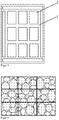
- An exemplary copper-ceramic composite in which the ceramic substrate 1 has a plurality of regions each provided with a coating 2 of copper or copper alloy is disclosed in US Pat FIG. 3 shown.
- the individual metallized areas can be replaced by predetermined breaking lines (not shown in FIG. 3 ) be separated from each other, so that a separation of these areas can be done by breaking along these predetermined breaking lines.
- the coating of copper or a copper alloy may at least partially have a structuring.
- the structuring of the metal coating can take place in a known manner, in particular via an etching process (for example using an etching mask).
- the copper or the copper alloy can be completely removed in partial areas, so that in these partial areas the surface of the ceramic substrate is exposed.
- the coating made of copper or a copper alloy to have one or more recesses (preferably round recesses) which are obtained, for example, in the etching process by only partially removing the copper or copper alloy in the region of the depression to be applied Therefore, the surface of the ceramic substrate in this area is still covered with copper or copper alloy.
- the ceramic substrate contains an oxide, a nitride, a carbide, or a mixture or composite of at least two of these materials.
- the ceramic substrate can consist of only one layer or alternatively of several layers.
- Suitable oxides include alumina (Al 2 O 3 ) or BeO. If the oxide is an aluminum oxide, this may optionally be reinforced with zirconium oxide (ZrO 2 ). Such a ZrO 2 -reinforced Al 2 O 3 , based on its total mass, usually contains the zirconium oxide in a proportion of 0.5-30% by weight.
- the zirconium oxide may optionally be doped with one or more doping oxide (s), in particular yttrium oxide, calcium oxide, cerium oxide or magnesium oxide, usually in an amount of up to 0.01% by weight or even up to 5% by weight, based on the total mass Zirconia and alumina.
- doping oxide s
- the ceramic substrate contains a nitride, this may be, for example, an aluminum nitride, a silicon nitride or a titanium nitride.
- the ceramic substrate may be a multilayer ceramic substrate containing at least one layer of aluminum nitride and at least one layer of Al 2 O 3 and wherein the coating of copper or a copper alloy is present on the layer of Al 2 O 3 .
- the ceramic substrate contains a carbide, this may be, for example, a silicon carbide.
- the ceramic substrate contains alumina (Al 2 O 3 ). As already mentioned above, this may be an Al 2 O 3 reinforced with ZrO 2 .
- the ceramic substrate preferably contains at least 65% by weight Al 2 O 3 . If no ZrO 2 is present for reinforcing the Al 2 O 3 , the ceramic substrate may for example consist of at least 95% by weight, preferably 96% by weight, of Al 2 O 3 .
- the ceramic substrate may be at least 96% by weight, more preferably at least 98% by weight, of this ZrO 2 -reinforced Al 2 O 3 consist.
- the particle sizes of the aluminum oxide are preferably in the range from 0.01 ⁇ m to 25 ⁇ m, more preferably in the range from 0.3 ⁇ m to 23 ⁇ m, even more preferably in the range from 0.5 ⁇ m to 20 ⁇ m.
- the ceramic substrate of the copper-ceramic composite has both high mechanical strength and high thermal conductivity.
- these values are not to be regarded as strict upper and lower limits for the particle size distribution, but may vary by +/- 10%. In a preferred embodiment, however, it is the lower limit, which is not exceeded, and upper limits, which is not exceeded, the grain size distribution of the alumina. In this preferred embodiment, therefore, the alumina has no grains which are outside the above ranges.
- d min (Al 2 O 3 ) ⁇ 0.01 ⁇ m and d max (Al 2 O 3 ) ⁇ 25 ⁇ m, more preferably d min (Al 2 O 3 ) ⁇ 0.3 ⁇ m and d max ( Al 2 O 3 ) ⁇ 23 ⁇ m, more preferably d min (Al 2 O 3 ) ⁇ 0.5 ⁇ m and d max (Al 2 O 3 ) ⁇ 20 ⁇ m, where d min (Al 2 O 3 ) and d max ( Al 2 O 3 ) are the minimum and maximum grain sizes of the alumina.
- the desired Al 2 O 3 Komuccn can be set in the copper-ceramic composite.
- Such ceramics are commercially available or can be obtained by standard methods.
- a fine adjustment of the grain sizes can optionally be done by a thermal treatment of the ceramic starting material.
- the distribution of the grain sizes is determined on the basis of the number of grains (ie grain size-number distribution).
- the alumina of the ceramic substrate has a number distribution of grain sizes in which at most 5% of the grains have a grain size of less than 0.1 ⁇ m, more preferably less than 0.3 ⁇ m, even more preferably less than 0.5 ⁇ m; and / or in which at least 95% of the grains have a particle size of less than 15 ⁇ m, more preferably less than 10 ⁇ m, even more preferably less than 7 ⁇ m.
- An improvement or optimization of the mechanical strength and the thermal conductivity of the ceramic substrate in the metal-ceramic composite can be achieved if the d 5 and d 95 values of the grain size distribution of Al 2 O 3 meet certain requirements.
- the number distribution of the grain sizes of the alumina has a d 95 value of ⁇ 15.0 ⁇ m, more preferably in the range of 4.0 ⁇ m to 15.0 ⁇ m, still more preferably in the range of 4.5 ⁇ m to 10.0 ⁇ m more preferably in the range of 5.0 microns to 8.0 microns.
- the d 5 value of the particle size distribution of the alumina is preferably ⁇ 0.1 ⁇ m; more preferably, the d 5 value is in the range of 0.1 ⁇ m to 2.5 ⁇ m, more preferably in the range of 0.3 ⁇ m to 2.5 ⁇ m, still more preferably in the range of 0.5 ⁇ m to 2.0 ⁇ m ,
- a further optimization of the mechanical strength and the thermal conductivity of the ceramic substrate in the metal-ceramic composite can be achieved.
- a preferred d 50 value of the particle size distribution of the aluminum oxide is, for example, in the range from 1.0 ⁇ m to 3.0 ⁇ m.
- the d5, d95 and d50 values of the grain size number distribution of the alumina are selected to satisfy the following condition: 9.5 ⁇ d 95 - d 5 / d 50 ⁇ 0.7
- the alumina has a number distribution of grain sizes with a median d 50 and an arithmetic mean d arith , the ratio of d 50 to d arith (ie d 50 / d arith , hereinafter also referred to as symmetry value S (Al 2 O 3 ) of the alumina particle size distribution) is in the range of 0.75 to 1.10, more preferably in the range of 0.78 to 1.05, still more preferably in the range of 0.80 to 1.00.
- symmetry value S Al 2 O 3
- Suitable methods by means of which the symmetry of the particle size distribution in the aluminum oxide, for example already during the preparation of the starting substrate, can be set are known to the person skilled in the art.
- the Symmetry of the particle size distribution can be influenced by sintering time and sintering temperature in the preparation of the starting substrate.
- Al 2 O 3 substrates, with which the above symmetry values can be realized in the final copper-ceramic composite, are commercially available or can be obtained by standard methods.
- the width of the particle size distribution can be expressed by the ratio of d 5 value to d 95 value.
- the alumina has a number distribution of grain sizes with a d 5 value and a d 95 value, the ratio of d 5 to d 95 being in the range of 0.1 to 0.4, more preferably in the range of 0 , 11 to 0.35, more preferably in the range of 0.12 to 0.30.
- the mean grain shape factor R a (Al 2 O 3 ) of the alumina is ⁇ 0.40, more preferably ⁇ 0.60, even more preferably ⁇ 0.80.
- Suitable methods by which the shape of the aluminum oxide grains can be adjusted, for example, already in the preparation of the starting substrate, are known to the person skilled in the art.
- the shape of the Al 2 O 3 grains may be affected by sintering time and sintering temperature in the preparation of the starting substrate.
- Al 2 O 3 substrates, with which the above-mentioned grain form factor R a (Al 2 O 3 ) can be realized in the final copper-ceramic composite, are commercially available or can be obtained by standard methods.
- a suitable thickness of the ceramic substrate in a copper-ceramic composite is known to those skilled in the art.
- the ceramic substrate has a thickness in the range of 0.2-1.2 mm over at least 70% of its area, more preferably at least 90% of its area.
- a thickness of the ceramic substrate is, for example, about 0.38 mm or about 0.63 mm.
- the thickness of the ceramic substrate (D cer ) and the median d 50 of the grain size number distribution of the alumina in the ceramic substrate are selected such that the ratio D cer to d 50 (ie D cer / d 50 ) ranges from 0.001 to 0.01 , more preferably in the range of 0.002 to 0.009, more preferably in the range of 0.004 to 0.008.
- the thickness D cer of the ceramic substrate is determined at one point and divided by the median d 50 of the particle size distribution of the alumina.
- the ratio D cer / d 50 is preferably at least over 70%, more preferably at least 90%, of the area of the ceramic substrate in the range of 0.05 to 0.40.
- the ceramic substrate may for example have a thermal conductivity of ⁇ 20 W / mK, and / or a bending strength of ⁇ 400 MPa.
- the ceramic substrate may be in the form of a single substrate.
- the ceramic substrate has one or more (preferably rectilinear) predetermined breaking lines, which divide the ceramic substrate into two or more areas and at least in one of these areas, the coating of copper or a copper alloy is applied.
- predetermined breaking lines can be exemplified DE 43 19 944 A1 and DE 199 27 046 A1 to get expelled.
- Suitable dimensions (length x width) of the ceramic substrate (either as a single substrate or as a multiple substrate) in a metal-ceramic composite are known to the person skilled in the art.
- the ceramic substrate may have a dimension, length x width, of (180-200 mm) x (130-150 mm) or (180-200 mm) x (270-290 mm). Even smaller dimensions, for example (8-12 mm) x (8-12 mm), are possible.
- Further improvement in the properties of the copper-ceramic composite can be realized by matching the grain properties of the copper or copper alloy and the grain properties of the aluminum oxide in the ceramic substrate.
- the ratio of d 50 (Al 2 O 3 ) to d 50 (Cu) is in the range of 0.008 to 0.055, more preferably in the range of 0.010 to 0.045.
- the alumina has a number distribution of grain sizes with a median value d 50
- an arithmetic mean d arith and a symmetry value S (Al 2 O 3 ) d 50 / d arith
- S (Al 2 O 3 ) and S (Cu) satisfy the following condition: 0.7 ⁇ S al 2 O 3 / S Cu ⁇ 1.4.
- S (Al 2 O 3 ) and S (Cu) satisfy the following condition: 0.74 ⁇ S al 2 O 3 / S Cu ⁇ 1.35 ; more preferably, the following condition 0.80 ⁇ S al 2 O 3 / S Cu ⁇ 1.25.
- the mean grain shape factor of the alumina R a (Al 2 O 3 ) and the average grain form factor of the copper or copper alloy R a (Cu) satisfy the following condition: 0.5 ⁇ R a (Al 2 O 3 ) / R a (Cu) ⁇ 2.0.
- the present invention relates to a module comprising at least one copper-ceramic composite according to the above description and one or more bonding wires.
- the bonding wire or wires are bonded to the copper or copper alloy coating. Suitable bonding methods for bonding wires to a metal coating are known to those skilled in the art.
- the module may also include one or more electronic components such as electronic components. contain one or more chips.
- the grain structures of the copper or of the copper alloy and of the aluminum oxide of the ceramic substrate are determined in the context of the present invention as follows:
- the grain sizes are determined by a line-cutting method. Line-cut methods are known to those skilled in the art and are described, for example, in ASTM 112-13.
- the magnification is chosen so that the line grid cuts at least 50 grains.
- two parallel lines in the x-direction and two parallel lines in the y-direction were respectively placed in the optical micrograph.
- the lines divide the recording into three equally wide stripes. This is in FIG. 4 shown schematically.
- this length L is taken as a grain size.
- a grain size is obtained.
- two values for a grain both of which are included in the determination of the particle size distribution.
- d 5 , d 50 and d 95 values and the arimethical mean d arith can be determined.
- the d 50 value which is frequently also referred to as median value
- 50% of the grains have a diameter which is smaller than the d 50 value.
- 5% of the grains have a diameter smaller than this d 5 value
- the d 95 value 95% of the grains have a diameter smaller than this d 95 value.
- the arithmetic mean of the particle size distribution results from the sum of the grain sizes of the individual grains divided by the number of cut grains.
- SEM image From the surface of the ceramic substrate, a scanning electron micrograph (SEM image) is taken. A special sample preparation in the form of a microsection is not required. The SEM photograph is taken at a location of the ceramic substrate that was previously copper-plated and exposed by etching.
- the grain sizes are determined by a line-cutting method. Line-cut methods are known to those skilled in the art and are described, for example, in ASTM 112-13.
- the magnification is chosen so that the line grid cuts at least 50 Al 2 O 3 grains. If the ceramic substrate still contains grains of a different chemical composition, for example ZrO 2 -Kömer, they can be distinguished well in the SEM image by means of secondary electron contrast from the Al 2 O 3 -Kömem and are therefore not included in the following calculations.
- a different chemical composition for example ZrO 2 -Kömer
- Both the grain sizes of the copper or the copper alloy and the grain sizes of the Al 2 O 3 are thus determined in a plane which is parallel to the coated substrate surface or coplanar with this.
- the light micrograph was used, which was also used in the determination of the particle size distribution.
- the following procedure is used to determine the shape factor of an individual grain: Its longest dimension d K, max is determined. Subsequently, at half the length of d K, max the diameter d K, ortho of the grain running perpendicular to d K, max is determined.
- the form factor is therefore also a measure of the circularity / roundness of the grains. See also FIG. 1 ,
- the form factor is determined for at least 50 grains of the light micrograph. Usually, the grains are evaluated, which were also cut in line intersection of the lines.
- the mean grain form factor of the copper or copper alloy then results from the arithmetic mean of the shape factors of the individual grains (i.e., the sum of the individual shape factors divided by the number of grains examined).
- the SEM image is used, which was also used to determine the particle size distribution.
- Both the grain shape factors of the copper and the copper alloy, as well as the grain shape factors of the Al 2 O 3 are thus determined in a plane which is parallel to the coplanar substrate surface or is coplanar with this.
- a typical process, which is preferably used in the context of the present invention for the application of the copper coating on the ceramic substrate is, for example, from the documents US 3,744,120 . US 3,994,430 . EP 0 085 914 A or the DE 23 19 854 A the disclosure of which is incorporated by reference into the present invention.
- this production method disclosed there is common in that a copper foil is first oxidized in such a way that a substantially uniform copper oxide layer results. The resulting copper foil is then positioned on a ceramic substrate and the ceramic substrate / copper foil composite is heated to a bonding temperature between about 1025-1083 ° C, thereby forming a metallized ceramic substrate. The copper foil thus forms a coating after bonding. Finally, the resulting metallized ceramic substrate is cooled.
- DCB process direct copper bonding process
- bonding furnaces The bonding of ceramic substrate and copper foil takes place in an oven, so-called bonding furnaces generally being used.
- bonding ovens often referred to as tunnel ovens include, inter alia, an elongated tunnel-like furnace chamber (also called muffle) and a transport device with a transport element, for example in the form of a flexible and heat-resistant conveyor belt for transporting the material to be treated by the heated furnace with a heater chamber.
- the ceramic substrates are positioned together with the copper foil on a carrier on the conveyor belt and then passed through in the bonding oven by the conveyor belt driven a heating area in which the required bonding temperature is reached.
- the resulting ceramic substrate / copper foil composite is recooled according to the invention.
- This method can be used in principle for the production of single-sidedly metallized ceramic substrates as well as for the production of double-sided metallized substrates.
- the production of double-sided metallized substrates usually takes place via a two-stage bonding process, i. using a two-stage single-layer process (SLB method).
- a two-stage bonding process is preferably used.
- the ceramic is bonded in two furnace passes to the copper foils on opposite sides of the ceramic substrate.
- a ceramic substrate is first positioned on a carrier and then covered on the overhead, ie on the side facing away from the carrier, with a copper foil.
- this side of the ceramic substrate is connected to the metal layer and subsequently the resulting assembly is cooled.
- the substrate is turned over and in a second bonding step, the other side of the substrate is provided in the same way with a metal layer, ie the copper foil.
- the following examples show how the shape factor of the grains of the copper coating affects the thermal shock resistance of a copper-ceramic composite.
- both the top and the bottom of the ceramic substrate was provided with a copper coating.
- the copper coating was first bonded to one side of the ceramic substrate by means of the SLB process.
- the opposite side of the ceramic substrate was made by the SLB method with another copper coating, so that a copper-ceramic substrate is formed in which a copper foil is bonded on both sides of the ceramic.
- One of the two copper coatings was subsequently patterned in each sample via an etching process (same structuring for all samples).
- the thickness of the copper coating was 0.3 mm and the length x width of the copper coating was 181 ⁇ 132 mm 2 .
- the exemplary embodiment is pure copper.
- both samples contained an Al 2 O 3 ceramic substrate (Al 2 O 3 content: 96% by weight), ceramic substrate thickness: 0.38 mm; Length x width of the ceramic substrate: 190 x 140 mm 2 .
- the choice of the copper coating was chosen so that the effect according to the invention, namely a good thermal shock resistance after the two-stage SLB bonding (inventive copper-ceramic substrate) was realized.
- FIG. 5 shows a light micrograph of the surface of the copper coating of KKV. 1
- the copper coating of KKV 2 had a mean shape factor R a (Cu) of 0.27.
- Table 1 below summarizes the results: Table 1: Thermal shock resistance of the copper-ceramic composites Thermal shock resistance Sample KKV 1 (according to the invention) Average grain form factor R a (Cu) of copper: 0.84 + Sample KKV 2 (comparison) Average grain form factor R a (Cu) of copper: 0.27 -
- the grain structure according to the invention which has a high proportion of relatively round or circular grains, to achieve an improvement in thermal shock resistance.
Landscapes
- Chemical & Material Sciences (AREA)
- Engineering & Computer Science (AREA)
- Ceramic Engineering (AREA)
- Materials Engineering (AREA)
- Structural Engineering (AREA)
- Organic Chemistry (AREA)
- Ceramic Products (AREA)
- Cooling Or The Like Of Semiconductors Or Solid State Devices (AREA)
Claims (8)
- Composite cuivre-céramique, comprenant :- un substrat en céramique,- un revêtement en cuivre ou en alliage de cuivre présent sur le substrat en céramique,les particules de cuivre ou de l'alliage de cuivre ayant à chaque fois un diamètre de particules maximal dK,max, un diamètre de particules dK,ortho s'étendant perpendiculairement à dK,max, déterminé à la moitié de la longueur de dK,max, et un facteur de forme RK=dK,ortho/dK,max et le cuivre ou l'alliage de cuivre présentant un facteur de forme de particules moyen Ra(Cu), déterminé comme moyenne arithmétique des facteurs de forme RK des particules de cuivre ou de l'alliage de cuivre, d'au moins 0,60, et le revêtement de cuivre ou d'alliage de cuivre étant appliqué par un procédé de métallisation directe au cuivre, DCB, sur le substrat en céramique.
- Composite cuivre-céramique selon la revendication 1, dans lequel les tailles de particules du cuivre ou de l'alliage de cuivre se situent dans la plage allant de 10 µm a 300 µm, de préférence dans la plage allant de 15 µm à 250 µm, de manière encore davantage préférée dans la plage allant de 20 µm à 210 µm.
- Composite cuivre-céramique selon la revendication 1 ou 2, dans lequel le facteur de forme moyen des particules Ra(Cu) du cuivre ou de l'alliage de cuivre est ≥ 0,80.
- Composite cuivre-céramique selon l'une quelconque des revendications précédentes, dans lequel le revêtement en cuivre ou en alliage de cuivre présente au moins en partie une structuration pour la formation de surfaces de contact électriques.
- Composite cuivre-céramique selon l'une quelconque des revendications précédentes, dans lequel le substrat en céramique contient un oxyde, un nitrure, un carbure ou un mélange ou composite d'au moins deux de ces matériaux.
- Composite cuivre-céramique selon l'une quelconque des revendications précédentes, dans lequel le substrat en céramique est constitué d'au moins 65 % en poids d'Al2O3 .
- Composite cuivre-céramique selon l'une quelconque des revendications précédentes, dans lequel le revêtement en cuivre ou en alliage de cuivre présente sur au moins 70 % de sa surface une épaisseur dans la plage allant de 0,2 à 1,2 mm ; et/ou le substrat en céramique présente sur au moins 70 % de sa surface une épaisseur dans la plage allant de 0,2 à 1,2 mm.
- Module, contenant au moins un composite cuivre-céramique selon l'une quelconque des revendications 1 à 7 et au moins un ou plusieurs fils de liaison.
Applications Claiming Priority (1)
| Application Number | Priority Date | Filing Date | Title |
|---|---|---|---|
| DE102016203038 | 2016-02-26 |
Publications (2)
| Publication Number | Publication Date |
|---|---|
| EP3210957A1 EP3210957A1 (fr) | 2017-08-30 |
| EP3210957B1 true EP3210957B1 (fr) | 2019-01-02 |
Family
ID=58261477
Family Applications (1)
| Application Number | Title | Priority Date | Filing Date |
|---|---|---|---|
| EP17156389.3A Active EP3210957B1 (fr) | 2016-02-26 | 2017-02-16 | Composite en ceramique/cuivre |
Country Status (1)
| Country | Link |
|---|---|
| EP (1) | EP3210957B1 (fr) |
Families Citing this family (1)
| Publication number | Priority date | Publication date | Assignee | Title |
|---|---|---|---|---|
| CN110379793A (zh) * | 2019-07-08 | 2019-10-25 | 上海申和热磁电子有限公司 | 一种覆铜陶瓷基板母板结构 |
Citations (7)
| Publication number | Priority date | Publication date | Assignee | Title |
|---|---|---|---|---|
| DE2319854A1 (de) | 1972-04-20 | 1973-10-25 | Gen Electric | Verfahren zum direkten verbinden von metallen mit nichtmetallischen substraten |
| DE102004012231B4 (de) | 2004-03-09 | 2006-03-23 | Curamik Electronics Gmbh | Metall-Keramik-Substrat |
| DE102004056879A1 (de) | 2004-10-27 | 2006-05-04 | Curamik Electronics Gmbh | Verfahren zum Herstellen eines Metall-Keramik-Substrates bzw. Kupfer-Keramik-Substrates sowie Träger zur Verwendung bei diesem Verfahren |
| DE19927046B4 (de) | 1999-06-14 | 2007-01-25 | Electrovac Ag | Keramik-Metall-Substrat als Mehrfachsubstrat |
| DE102009033029A1 (de) | 2009-07-02 | 2011-01-05 | Electrovac Ag | Elektronische Vorrichtung |
| DE102012110322B4 (de) | 2012-10-29 | 2014-09-11 | Rogers Germany Gmbh | Metall-Keramik-Substrat sowie Verfahren zum Herstellen eines Metall-Keramik-Substrates |
| DE102013104739A1 (de) | 2013-03-14 | 2014-09-18 | Rogers Germany Gmbh | Metall-Keramik-Substrat sowie Verfahren zum Herstellen eines Metall-Keramik-Substrates |
Family Cites Families (8)
| Publication number | Priority date | Publication date | Assignee | Title |
|---|---|---|---|---|
| US3744120A (en) | 1972-04-20 | 1973-07-10 | Gen Electric | Direct bonding of metals with a metal-gas eutectic |
| US3994430A (en) | 1975-07-30 | 1976-11-30 | General Electric Company | Direct bonding of metals to ceramics and metals |
| DE3204167A1 (de) | 1982-02-06 | 1983-08-11 | Brown, Boveri & Cie Ag, 6800 Mannheim | Verfahren zum direkten verbinden von metallstuecken mit oxidkeramiksubstraten |
| DE4004844C1 (de) | 1990-02-16 | 1991-01-03 | Abb Ixys Semiconductor Gmbh | Verfahren zur Herstellung einer strukturierten Kupfermetallisierung auf einem Keramiksubstrat |
| DE4318241C2 (de) | 1993-06-02 | 1995-06-29 | Schulz Harder Juergen | Metallbeschichtetes Substrat mit verbesserter Widerstandsfähigkeit gegen Temperaturwechselbeanspruchung |
| DE4319944C2 (de) | 1993-06-03 | 1998-07-23 | Schulz Harder Juergen | Mehrfach-Substrat sowie Verfahren zu seiner Herstellung |
| US7476422B2 (en) * | 2002-05-23 | 2009-01-13 | Delphi Technologies, Inc. | Copper circuit formed by kinetic spray |
| JP6130209B2 (ja) * | 2013-05-14 | 2017-05-17 | Dowaエレクトロニクス株式会社 | 導電膜 |
-
2017
- 2017-02-16 EP EP17156389.3A patent/EP3210957B1/fr active Active
Patent Citations (7)
| Publication number | Priority date | Publication date | Assignee | Title |
|---|---|---|---|---|
| DE2319854A1 (de) | 1972-04-20 | 1973-10-25 | Gen Electric | Verfahren zum direkten verbinden von metallen mit nichtmetallischen substraten |
| DE19927046B4 (de) | 1999-06-14 | 2007-01-25 | Electrovac Ag | Keramik-Metall-Substrat als Mehrfachsubstrat |
| DE102004012231B4 (de) | 2004-03-09 | 2006-03-23 | Curamik Electronics Gmbh | Metall-Keramik-Substrat |
| DE102004056879A1 (de) | 2004-10-27 | 2006-05-04 | Curamik Electronics Gmbh | Verfahren zum Herstellen eines Metall-Keramik-Substrates bzw. Kupfer-Keramik-Substrates sowie Träger zur Verwendung bei diesem Verfahren |
| DE102009033029A1 (de) | 2009-07-02 | 2011-01-05 | Electrovac Ag | Elektronische Vorrichtung |
| DE102012110322B4 (de) | 2012-10-29 | 2014-09-11 | Rogers Germany Gmbh | Metall-Keramik-Substrat sowie Verfahren zum Herstellen eines Metall-Keramik-Substrates |
| DE102013104739A1 (de) | 2013-03-14 | 2014-09-18 | Rogers Germany Gmbh | Metall-Keramik-Substrat sowie Verfahren zum Herstellen eines Metall-Keramik-Substrates |
Also Published As
| Publication number | Publication date |
|---|---|
| EP3210957A1 (fr) | 2017-08-30 |
Similar Documents
| Publication | Publication Date | Title |
|---|---|---|
| DE10141910B4 (de) | Glaskeramiksinterprodukt und Verfahren zu seiner Herstellung | |
| EP3419950B1 (fr) | Composite cuivre-ceramique | |
| DE69317342T2 (de) | Leiterplatte aus Aluminiumnitrid und Verfahren zu ihrer Herstellung | |
| DE69713540T2 (de) | Siliziumnitrid-Platine und ihre Herstellung | |
| DE112018000457T5 (de) | Isoliertes wärmeableitungssubstrat | |
| DE60300230T2 (de) | Glas-Keramik-Zusammensetzung, Glas-Keramik gesintertes Material und keramisches Mehrschichtsubstrat | |
| DE102005042554B4 (de) | Metall-Keramik-Substrat und Verfahren zur Herstellung eines Metall-Keramik-Substrats | |
| EP3210956B1 (fr) | Composite en ceramique/cuivre | |
| EP3419949B1 (fr) | Composite en ceramique/cuivre | |
| EP3419952B1 (fr) | Composite cuivre-ceramique | |
| EP3210951B1 (fr) | Composite en ceramique/cuivre | |
| DE10120641B4 (de) | Keramik mit sehr guten Hochfrequenzeigenschaften und Verfahren zu ihrer Herstellung | |
| EP3419951B1 (fr) | Composite cuivre-ceramique | |
| DE69934909T2 (de) | Substrat auf der basis eines siliziumnitridkomposits | |
| EP3210957B1 (fr) | Composite en ceramique/cuivre | |
| EP4237390B1 (fr) | Substrat en cuivre-céramique | |
| DE102016203097B3 (de) | Kupfer-Keramik-Verbund und Modul | |
| DE112021000182T5 (de) | Keramiksinterkörper und Substrat für eine Halbleitervorrichtung | |
| DE202016008371U1 (de) | Kupfer-Keramik-Verbund | |
| DE202016008286U1 (de) | Kupfer-Keramik-Verbund | |
| DE202016008370U1 (de) | Kupfer-Keramik-Verbund | |
| DE202016008287U1 (de) | Kupfer-Keramik-Verbund | |
| DE202016008307U1 (de) | Kupfer-Keramik-Verbund | |
| DE112022007831T5 (de) | Substrat für eine halbleitervorrichtung und verfahren zur herstellung davon | |
| EP4644351A2 (fr) | Procédé de fabrication d'un substrat métal-céramique, élément céramique et couche métallique pour un tel procédé et substrat métal-céramique fabriqué par un tel procédé |
Legal Events
| Date | Code | Title | Description |
|---|---|---|---|
| PUAI | Public reference made under article 153(3) epc to a published international application that has entered the european phase |
Free format text: ORIGINAL CODE: 0009012 |
|
| STAA | Information on the status of an ep patent application or granted ep patent |
Free format text: STATUS: THE APPLICATION HAS BEEN PUBLISHED |
|
| AK | Designated contracting states |
Kind code of ref document: A1 Designated state(s): AL AT BE BG CH CY CZ DE DK EE ES FI FR GB GR HR HU IE IS IT LI LT LU LV MC MK MT NL NO PL PT RO RS SE SI SK SM TR |
|
| AX | Request for extension of the european patent |
Extension state: BA ME |
|
| STAA | Information on the status of an ep patent application or granted ep patent |
Free format text: STATUS: REQUEST FOR EXAMINATION WAS MADE |
|
| 17P | Request for examination filed |
Effective date: 20180228 |
|
| RBV | Designated contracting states (corrected) |
Designated state(s): AL AT BE BG CH CY CZ DE DK EE ES FI FR GB GR HR HU IE IS IT LI LT LU LV MC MK MT NL NO PL PT RO RS SE SI SK SM TR |
|
| GRAP | Despatch of communication of intention to grant a patent |
Free format text: ORIGINAL CODE: EPIDOSNIGR1 |
|
| STAA | Information on the status of an ep patent application or granted ep patent |
Free format text: STATUS: GRANT OF PATENT IS INTENDED |
|
| INTG | Intention to grant announced |
Effective date: 20181011 |
|
| RIN1 | Information on inventor provided before grant (corrected) |
Inventor name: HERBST, KAI Inventor name: MUSCHELKNAUTZ, CHRISTIAN |
|
| GRAS | Grant fee paid |
Free format text: ORIGINAL CODE: EPIDOSNIGR3 |
|
| GRAA | (expected) grant |
Free format text: ORIGINAL CODE: 0009210 |
|
| STAA | Information on the status of an ep patent application or granted ep patent |
Free format text: STATUS: THE PATENT HAS BEEN GRANTED |
|
| AK | Designated contracting states |
Kind code of ref document: B1 Designated state(s): AL AT BE BG CH CY CZ DE DK EE ES FI FR GB GR HR HU IE IS IT LI LT LU LV MC MK MT NL NO PL PT RO RS SE SI SK SM TR |
|
| REG | Reference to a national code |
Ref country code: GB Ref legal event code: FG4D Free format text: NOT ENGLISH |
|
| REG | Reference to a national code |
Ref country code: CH Ref legal event code: EP Ref country code: AT Ref legal event code: REF Ref document number: 1084164 Country of ref document: AT Kind code of ref document: T Effective date: 20190115 |
|
| REG | Reference to a national code |
Ref country code: IE Ref legal event code: FG4D Free format text: LANGUAGE OF EP DOCUMENT: GERMAN |
|
| REG | Reference to a national code |
Ref country code: DE Ref legal event code: R096 Ref document number: 502017000581 Country of ref document: DE |
|
| REG | Reference to a national code |
Ref country code: CH Ref legal event code: NV Representative=s name: DENNEMEYER AG, CH |
|
| REG | Reference to a national code |
Ref country code: NL Ref legal event code: MP Effective date: 20190102 |
|
| REG | Reference to a national code |
Ref country code: LT Ref legal event code: MG4D |
|
| PG25 | Lapsed in a contracting state [announced via postgrant information from national office to epo] |
Ref country code: NL Free format text: LAPSE BECAUSE OF FAILURE TO SUBMIT A TRANSLATION OF THE DESCRIPTION OR TO PAY THE FEE WITHIN THE PRESCRIBED TIME-LIMIT Effective date: 20190102 |
|
| PG25 | Lapsed in a contracting state [announced via postgrant information from national office to epo] |
Ref country code: PL Free format text: LAPSE BECAUSE OF FAILURE TO SUBMIT A TRANSLATION OF THE DESCRIPTION OR TO PAY THE FEE WITHIN THE PRESCRIBED TIME-LIMIT Effective date: 20190102 Ref country code: NO Free format text: LAPSE BECAUSE OF FAILURE TO SUBMIT A TRANSLATION OF THE DESCRIPTION OR TO PAY THE FEE WITHIN THE PRESCRIBED TIME-LIMIT Effective date: 20190402 Ref country code: SE Free format text: LAPSE BECAUSE OF FAILURE TO SUBMIT A TRANSLATION OF THE DESCRIPTION OR TO PAY THE FEE WITHIN THE PRESCRIBED TIME-LIMIT Effective date: 20190102 Ref country code: FI Free format text: LAPSE BECAUSE OF FAILURE TO SUBMIT A TRANSLATION OF THE DESCRIPTION OR TO PAY THE FEE WITHIN THE PRESCRIBED TIME-LIMIT Effective date: 20190102 Ref country code: PT Free format text: LAPSE BECAUSE OF FAILURE TO SUBMIT A TRANSLATION OF THE DESCRIPTION OR TO PAY THE FEE WITHIN THE PRESCRIBED TIME-LIMIT Effective date: 20190502 Ref country code: ES Free format text: LAPSE BECAUSE OF FAILURE TO SUBMIT A TRANSLATION OF THE DESCRIPTION OR TO PAY THE FEE WITHIN THE PRESCRIBED TIME-LIMIT Effective date: 20190102 Ref country code: LT Free format text: LAPSE BECAUSE OF FAILURE TO SUBMIT A TRANSLATION OF THE DESCRIPTION OR TO PAY THE FEE WITHIN THE PRESCRIBED TIME-LIMIT Effective date: 20190102 |
|
| PG25 | Lapsed in a contracting state [announced via postgrant information from national office to epo] |
Ref country code: LV Free format text: LAPSE BECAUSE OF FAILURE TO SUBMIT A TRANSLATION OF THE DESCRIPTION OR TO PAY THE FEE WITHIN THE PRESCRIBED TIME-LIMIT Effective date: 20190102 Ref country code: HR Free format text: LAPSE BECAUSE OF FAILURE TO SUBMIT A TRANSLATION OF THE DESCRIPTION OR TO PAY THE FEE WITHIN THE PRESCRIBED TIME-LIMIT Effective date: 20190102 Ref country code: GR Free format text: LAPSE BECAUSE OF FAILURE TO SUBMIT A TRANSLATION OF THE DESCRIPTION OR TO PAY THE FEE WITHIN THE PRESCRIBED TIME-LIMIT Effective date: 20190403 Ref country code: IS Free format text: LAPSE BECAUSE OF FAILURE TO SUBMIT A TRANSLATION OF THE DESCRIPTION OR TO PAY THE FEE WITHIN THE PRESCRIBED TIME-LIMIT Effective date: 20190502 Ref country code: BG Free format text: LAPSE BECAUSE OF FAILURE TO SUBMIT A TRANSLATION OF THE DESCRIPTION OR TO PAY THE FEE WITHIN THE PRESCRIBED TIME-LIMIT Effective date: 20190402 Ref country code: RS Free format text: LAPSE BECAUSE OF FAILURE TO SUBMIT A TRANSLATION OF THE DESCRIPTION OR TO PAY THE FEE WITHIN THE PRESCRIBED TIME-LIMIT Effective date: 20190102 |
|
| REG | Reference to a national code |
Ref country code: DE Ref legal event code: R026 Ref document number: 502017000581 Country of ref document: DE |
|
| PLBI | Opposition filed |
Free format text: ORIGINAL CODE: 0009260 |
|
| PLAX | Notice of opposition and request to file observation + time limit sent |
Free format text: ORIGINAL CODE: EPIDOSNOBS2 |
|
| PG25 | Lapsed in a contracting state [announced via postgrant information from national office to epo] |
Ref country code: DK Free format text: LAPSE BECAUSE OF FAILURE TO SUBMIT A TRANSLATION OF THE DESCRIPTION OR TO PAY THE FEE WITHIN THE PRESCRIBED TIME-LIMIT Effective date: 20190102 Ref country code: EE Free format text: LAPSE BECAUSE OF FAILURE TO SUBMIT A TRANSLATION OF THE DESCRIPTION OR TO PAY THE FEE WITHIN THE PRESCRIBED TIME-LIMIT Effective date: 20190102 Ref country code: SK Free format text: LAPSE BECAUSE OF FAILURE TO SUBMIT A TRANSLATION OF THE DESCRIPTION OR TO PAY THE FEE WITHIN THE PRESCRIBED TIME-LIMIT Effective date: 20190102 Ref country code: LU Free format text: LAPSE BECAUSE OF NON-PAYMENT OF DUE FEES Effective date: 20190216 Ref country code: RO Free format text: LAPSE BECAUSE OF FAILURE TO SUBMIT A TRANSLATION OF THE DESCRIPTION OR TO PAY THE FEE WITHIN THE PRESCRIBED TIME-LIMIT Effective date: 20190102 Ref country code: IT Free format text: LAPSE BECAUSE OF FAILURE TO SUBMIT A TRANSLATION OF THE DESCRIPTION OR TO PAY THE FEE WITHIN THE PRESCRIBED TIME-LIMIT Effective date: 20190102 Ref country code: CZ Free format text: LAPSE BECAUSE OF FAILURE TO SUBMIT A TRANSLATION OF THE DESCRIPTION OR TO PAY THE FEE WITHIN THE PRESCRIBED TIME-LIMIT Effective date: 20190102 Ref country code: AL Free format text: LAPSE BECAUSE OF FAILURE TO SUBMIT A TRANSLATION OF THE DESCRIPTION OR TO PAY THE FEE WITHIN THE PRESCRIBED TIME-LIMIT Effective date: 20190102 Ref country code: MC Free format text: LAPSE BECAUSE OF FAILURE TO SUBMIT A TRANSLATION OF THE DESCRIPTION OR TO PAY THE FEE WITHIN THE PRESCRIBED TIME-LIMIT Effective date: 20190102 |
|
| 26 | Opposition filed |
Opponent name: ROGERS GERMANY GMBH Effective date: 20191002 |
|
| REG | Reference to a national code |
Ref country code: BE Ref legal event code: MM Effective date: 20190228 |
|
| REG | Reference to a national code |
Ref country code: IE Ref legal event code: MM4A |
|
| PG25 | Lapsed in a contracting state [announced via postgrant information from national office to epo] |
Ref country code: SM Free format text: LAPSE BECAUSE OF FAILURE TO SUBMIT A TRANSLATION OF THE DESCRIPTION OR TO PAY THE FEE WITHIN THE PRESCRIBED TIME-LIMIT Effective date: 20190102 |
|
| PG25 | Lapsed in a contracting state [announced via postgrant information from national office to epo] |
Ref country code: IE Free format text: LAPSE BECAUSE OF NON-PAYMENT OF DUE FEES Effective date: 20190216 |
|
| PG25 | Lapsed in a contracting state [announced via postgrant information from national office to epo] |
Ref country code: SI Free format text: LAPSE BECAUSE OF FAILURE TO SUBMIT A TRANSLATION OF THE DESCRIPTION OR TO PAY THE FEE WITHIN THE PRESCRIBED TIME-LIMIT Effective date: 20190102 Ref country code: BE Free format text: LAPSE BECAUSE OF NON-PAYMENT OF DUE FEES Effective date: 20190228 |
|
| PLBB | Reply of patent proprietor to notice(s) of opposition received |
Free format text: ORIGINAL CODE: EPIDOSNOBS3 |
|
| PG25 | Lapsed in a contracting state [announced via postgrant information from national office to epo] |
Ref country code: TR Free format text: LAPSE BECAUSE OF FAILURE TO SUBMIT A TRANSLATION OF THE DESCRIPTION OR TO PAY THE FEE WITHIN THE PRESCRIBED TIME-LIMIT Effective date: 20190102 |
|
| PG25 | Lapsed in a contracting state [announced via postgrant information from national office to epo] |
Ref country code: MT Free format text: LAPSE BECAUSE OF FAILURE TO SUBMIT A TRANSLATION OF THE DESCRIPTION OR TO PAY THE FEE WITHIN THE PRESCRIBED TIME-LIMIT Effective date: 20190102 |
|
| PG25 | Lapsed in a contracting state [announced via postgrant information from national office to epo] |
Ref country code: CY Free format text: LAPSE BECAUSE OF FAILURE TO SUBMIT A TRANSLATION OF THE DESCRIPTION OR TO PAY THE FEE WITHIN THE PRESCRIBED TIME-LIMIT Effective date: 20190102 |
|
| PG25 | Lapsed in a contracting state [announced via postgrant information from national office to epo] |
Ref country code: HU Free format text: LAPSE BECAUSE OF FAILURE TO SUBMIT A TRANSLATION OF THE DESCRIPTION OR TO PAY THE FEE WITHIN THE PRESCRIBED TIME-LIMIT; INVALID AB INITIO Effective date: 20170216 |
|
| PLBP | Opposition withdrawn |
Free format text: ORIGINAL CODE: 0009264 |
|
| GBPC | Gb: european patent ceased through non-payment of renewal fee |
Effective date: 20210216 |
|
| PLBD | Termination of opposition procedure: decision despatched |
Free format text: ORIGINAL CODE: EPIDOSNOPC1 |
|
| REG | Reference to a national code |
Ref country code: DE Ref legal event code: R100 Ref document number: 502017000581 Country of ref document: DE |
|
| PG25 | Lapsed in a contracting state [announced via postgrant information from national office to epo] |
Ref country code: GB Free format text: LAPSE BECAUSE OF NON-PAYMENT OF DUE FEES Effective date: 20210216 |
|
| PLBM | Termination of opposition procedure: date of legal effect published |
Free format text: ORIGINAL CODE: 0009276 |
|
| 27C | Opposition proceedings terminated |
Effective date: 20211118 |
|
| PG25 | Lapsed in a contracting state [announced via postgrant information from national office to epo] |
Ref country code: MK Free format text: LAPSE BECAUSE OF FAILURE TO SUBMIT A TRANSLATION OF THE DESCRIPTION OR TO PAY THE FEE WITHIN THE PRESCRIBED TIME-LIMIT Effective date: 20190102 |
|
| REG | Reference to a national code |
Ref country code: AT Ref legal event code: MM01 Ref document number: 1084164 Country of ref document: AT Kind code of ref document: T Effective date: 20220216 |
|
| PG25 | Lapsed in a contracting state [announced via postgrant information from national office to epo] |
Ref country code: AT Free format text: LAPSE BECAUSE OF NON-PAYMENT OF DUE FEES Effective date: 20220216 |
|
| P01 | Opt-out of the competence of the unified patent court (upc) registered |
Effective date: 20230527 |
|
| REG | Reference to a national code |
Ref country code: DE Ref legal event code: R082 Ref document number: 502017000581 Country of ref document: DE Ref country code: DE Ref legal event code: R081 Ref document number: 502017000581 Country of ref document: DE Owner name: HERAEUS ELECTRONICS GMBH & CO. KG, DE Free format text: FORMER OWNER: HERAEUS DEUTSCHLAND GMBH & CO. KG, 63450 HANAU, DE |
|
| REG | Reference to a national code |
Ref country code: CH Ref legal event code: U11 Free format text: ST27 STATUS EVENT CODE: U-0-0-U10-U11 (AS PROVIDED BY THE NATIONAL OFFICE) Effective date: 20260301 |
|
| PGFP | Annual fee paid to national office [announced via postgrant information from national office to epo] |
Ref country code: DE Payment date: 20260218 Year of fee payment: 10 |
|
| PGFP | Annual fee paid to national office [announced via postgrant information from national office to epo] |
Ref country code: FR Payment date: 20260218 Year of fee payment: 10 |
|
| PGFP | Annual fee paid to national office [announced via postgrant information from national office to epo] |
Ref country code: CH Payment date: 20260301 Year of fee payment: 10 |