EP4237390B1 - Substrat en cuivre-céramique - Google Patents
Substrat en cuivre-céramique Download PDFInfo
- Publication number
- EP4237390B1 EP4237390B1 EP21805423.7A EP21805423A EP4237390B1 EP 4237390 B1 EP4237390 B1 EP 4237390B1 EP 21805423 A EP21805423 A EP 21805423A EP 4237390 B1 EP4237390 B1 EP 4237390B1
- Authority
- EP
- European Patent Office
- Prior art keywords
- copper
- ppm
- copper layer
- ceramic substrate
- content
- Prior art date
- Legal status (The legal status is an assumption and is not a legal conclusion. Google has not performed a legal analysis and makes no representation as to the accuracy of the status listed.)
- Active
Links
Images

Classifications
-
- C—CHEMISTRY; METALLURGY
- C04—CEMENTS; CONCRETE; ARTIFICIAL STONE; CERAMICS; REFRACTORIES
- C04B—LIME, MAGNESIA; SLAG; CEMENTS; COMPOSITIONS THEREOF, e.g. MORTARS, CONCRETE OR LIKE BUILDING MATERIALS; ARTIFICIAL STONE; CERAMICS; REFRACTORIES; TREATMENT OF NATURAL STONE
- C04B37/00—Joining burned ceramic articles with other burned ceramic articles or other articles by heating
- C04B37/02—Joining burned ceramic articles with other burned ceramic articles or other articles by heating with metallic articles
-
- B—PERFORMING OPERATIONS; TRANSPORTING
- B32—LAYERED PRODUCTS
- B32B—LAYERED PRODUCTS, i.e. PRODUCTS BUILT-UP OF STRATA OF FLAT OR NON-FLAT, e.g. CELLULAR OR HONEYCOMB, FORM
- B32B15/00—Layered products comprising a layer of metal
- B32B15/20—Layered products comprising a layer of metal comprising aluminium or copper
-
- B—PERFORMING OPERATIONS; TRANSPORTING
- B32—LAYERED PRODUCTS
- B32B—LAYERED PRODUCTS, i.e. PRODUCTS BUILT-UP OF STRATA OF FLAT OR NON-FLAT, e.g. CELLULAR OR HONEYCOMB, FORM
- B32B9/00—Layered products comprising a layer of a particular substance not covered by groups B32B11/00 - B32B29/00
- B32B9/005—Layered products comprising a layer of a particular substance not covered by groups B32B11/00 - B32B29/00 comprising one layer of ceramic material, e.g. porcelain, ceramic tile
-
- B—PERFORMING OPERATIONS; TRANSPORTING
- B32—LAYERED PRODUCTS
- B32B—LAYERED PRODUCTS, i.e. PRODUCTS BUILT-UP OF STRATA OF FLAT OR NON-FLAT, e.g. CELLULAR OR HONEYCOMB, FORM
- B32B9/00—Layered products comprising a layer of a particular substance not covered by groups B32B11/00 - B32B29/00
- B32B9/04—Layered products comprising a layer of a particular substance not covered by groups B32B11/00 - B32B29/00 comprising such particular substance as the main or only constituent of a layer, which is next to another layer of the same or of a different material
- B32B9/041—Layered products comprising a layer of a particular substance not covered by groups B32B11/00 - B32B29/00 comprising such particular substance as the main or only constituent of a layer, which is next to another layer of the same or of a different material of metal
-
- C—CHEMISTRY; METALLURGY
- C04—CEMENTS; CONCRETE; ARTIFICIAL STONE; CERAMICS; REFRACTORIES
- C04B—LIME, MAGNESIA; SLAG; CEMENTS; COMPOSITIONS THEREOF, e.g. MORTARS, CONCRETE OR LIKE BUILDING MATERIALS; ARTIFICIAL STONE; CERAMICS; REFRACTORIES; TREATMENT OF NATURAL STONE
- C04B37/00—Joining burned ceramic articles with other burned ceramic articles or other articles by heating
- C04B37/02—Joining burned ceramic articles with other burned ceramic articles or other articles by heating with metallic articles
- C04B37/021—Joining burned ceramic articles with other burned ceramic articles or other articles by heating with metallic articles in a direct manner, e.g. direct copper bonding [DCB]
-
- C—CHEMISTRY; METALLURGY
- C04—CEMENTS; CONCRETE; ARTIFICIAL STONE; CERAMICS; REFRACTORIES
- C04B—LIME, MAGNESIA; SLAG; CEMENTS; COMPOSITIONS THEREOF, e.g. MORTARS, CONCRETE OR LIKE BUILDING MATERIALS; ARTIFICIAL STONE; CERAMICS; REFRACTORIES; TREATMENT OF NATURAL STONE
- C04B37/00—Joining burned ceramic articles with other burned ceramic articles or other articles by heating
- C04B37/02—Joining burned ceramic articles with other burned ceramic articles or other articles by heating with metallic articles
- C04B37/023—Joining burned ceramic articles with other burned ceramic articles or other articles by heating with metallic articles characterised by the interlayer used
- C04B37/025—Joining burned ceramic articles with other burned ceramic articles or other articles by heating with metallic articles characterised by the interlayer used consisting of glass or ceramic material
-
- C—CHEMISTRY; METALLURGY
- C04—CEMENTS; CONCRETE; ARTIFICIAL STONE; CERAMICS; REFRACTORIES
- C04B—LIME, MAGNESIA; SLAG; CEMENTS; COMPOSITIONS THEREOF, e.g. MORTARS, CONCRETE OR LIKE BUILDING MATERIALS; ARTIFICIAL STONE; CERAMICS; REFRACTORIES; TREATMENT OF NATURAL STONE
- C04B37/00—Joining burned ceramic articles with other burned ceramic articles or other articles by heating
- C04B37/02—Joining burned ceramic articles with other burned ceramic articles or other articles by heating with metallic articles
- C04B37/023—Joining burned ceramic articles with other burned ceramic articles or other articles by heating with metallic articles characterised by the interlayer used
- C04B37/026—Joining burned ceramic articles with other burned ceramic articles or other articles by heating with metallic articles characterised by the interlayer used consisting of metals or metal salts
-
- B—PERFORMING OPERATIONS; TRANSPORTING
- B32—LAYERED PRODUCTS
- B32B—LAYERED PRODUCTS, i.e. PRODUCTS BUILT-UP OF STRATA OF FLAT OR NON-FLAT, e.g. CELLULAR OR HONEYCOMB, FORM
- B32B2307/00—Properties of the layers or laminate
- B32B2307/50—Properties of the layers or laminate having particular mechanical properties
- B32B2307/536—Hardness
-
- C—CHEMISTRY; METALLURGY
- C04—CEMENTS; CONCRETE; ARTIFICIAL STONE; CERAMICS; REFRACTORIES
- C04B—LIME, MAGNESIA; SLAG; CEMENTS; COMPOSITIONS THEREOF, e.g. MORTARS, CONCRETE OR LIKE BUILDING MATERIALS; ARTIFICIAL STONE; CERAMICS; REFRACTORIES; TREATMENT OF NATURAL STONE
- C04B2237/00—Aspects relating to ceramic laminates or to joining of ceramic articles with other articles by heating
- C04B2237/02—Aspects relating to interlayers, e.g. used to join ceramic articles with other articles by heating
- C04B2237/04—Ceramic interlayers
- C04B2237/06—Oxidic interlayers
- C04B2237/064—Oxidic interlayers based on alumina or aluminates
-
- C—CHEMISTRY; METALLURGY
- C04—CEMENTS; CONCRETE; ARTIFICIAL STONE; CERAMICS; REFRACTORIES
- C04B—LIME, MAGNESIA; SLAG; CEMENTS; COMPOSITIONS THEREOF, e.g. MORTARS, CONCRETE OR LIKE BUILDING MATERIALS; ARTIFICIAL STONE; CERAMICS; REFRACTORIES; TREATMENT OF NATURAL STONE
- C04B2237/00—Aspects relating to ceramic laminates or to joining of ceramic articles with other articles by heating
- C04B2237/02—Aspects relating to interlayers, e.g. used to join ceramic articles with other articles by heating
- C04B2237/12—Metallic interlayers
- C04B2237/124—Metallic interlayers based on copper
-
- C—CHEMISTRY; METALLURGY
- C04—CEMENTS; CONCRETE; ARTIFICIAL STONE; CERAMICS; REFRACTORIES
- C04B—LIME, MAGNESIA; SLAG; CEMENTS; COMPOSITIONS THEREOF, e.g. MORTARS, CONCRETE OR LIKE BUILDING MATERIALS; ARTIFICIAL STONE; CERAMICS; REFRACTORIES; TREATMENT OF NATURAL STONE
- C04B2237/00—Aspects relating to ceramic laminates or to joining of ceramic articles with other articles by heating
- C04B2237/02—Aspects relating to interlayers, e.g. used to join ceramic articles with other articles by heating
- C04B2237/12—Metallic interlayers
- C04B2237/126—Metallic interlayers wherein the active component for bonding is not the largest fraction of the interlayer
- C04B2237/127—The active component for bonding being a refractory metal
-
- C—CHEMISTRY; METALLURGY
- C04—CEMENTS; CONCRETE; ARTIFICIAL STONE; CERAMICS; REFRACTORIES
- C04B—LIME, MAGNESIA; SLAG; CEMENTS; COMPOSITIONS THEREOF, e.g. MORTARS, CONCRETE OR LIKE BUILDING MATERIALS; ARTIFICIAL STONE; CERAMICS; REFRACTORIES; TREATMENT OF NATURAL STONE
- C04B2237/00—Aspects relating to ceramic laminates or to joining of ceramic articles with other articles by heating
- C04B2237/02—Aspects relating to interlayers, e.g. used to join ceramic articles with other articles by heating
- C04B2237/12—Metallic interlayers
- C04B2237/126—Metallic interlayers wherein the active component for bonding is not the largest fraction of the interlayer
- C04B2237/128—The active component for bonding being silicon
-
- C—CHEMISTRY; METALLURGY
- C04—CEMENTS; CONCRETE; ARTIFICIAL STONE; CERAMICS; REFRACTORIES
- C04B—LIME, MAGNESIA; SLAG; CEMENTS; COMPOSITIONS THEREOF, e.g. MORTARS, CONCRETE OR LIKE BUILDING MATERIALS; ARTIFICIAL STONE; CERAMICS; REFRACTORIES; TREATMENT OF NATURAL STONE
- C04B2237/00—Aspects relating to ceramic laminates or to joining of ceramic articles with other articles by heating
- C04B2237/30—Composition of layers of ceramic laminates or of ceramic or metallic articles to be joined by heating, e.g. Si substrates
- C04B2237/32—Ceramic
- C04B2237/34—Oxidic
- C04B2237/343—Alumina or aluminates
-
- C—CHEMISTRY; METALLURGY
- C04—CEMENTS; CONCRETE; ARTIFICIAL STONE; CERAMICS; REFRACTORIES
- C04B—LIME, MAGNESIA; SLAG; CEMENTS; COMPOSITIONS THEREOF, e.g. MORTARS, CONCRETE OR LIKE BUILDING MATERIALS; ARTIFICIAL STONE; CERAMICS; REFRACTORIES; TREATMENT OF NATURAL STONE
- C04B2237/00—Aspects relating to ceramic laminates or to joining of ceramic articles with other articles by heating
- C04B2237/30—Composition of layers of ceramic laminates or of ceramic or metallic articles to be joined by heating, e.g. Si substrates
- C04B2237/32—Ceramic
- C04B2237/34—Oxidic
- C04B2237/345—Refractory metal oxides
- C04B2237/348—Zirconia, hafnia, zirconates or hafnates
-
- C—CHEMISTRY; METALLURGY
- C04—CEMENTS; CONCRETE; ARTIFICIAL STONE; CERAMICS; REFRACTORIES
- C04B—LIME, MAGNESIA; SLAG; CEMENTS; COMPOSITIONS THEREOF, e.g. MORTARS, CONCRETE OR LIKE BUILDING MATERIALS; ARTIFICIAL STONE; CERAMICS; REFRACTORIES; TREATMENT OF NATURAL STONE
- C04B2237/00—Aspects relating to ceramic laminates or to joining of ceramic articles with other articles by heating
- C04B2237/30—Composition of layers of ceramic laminates or of ceramic or metallic articles to be joined by heating, e.g. Si substrates
- C04B2237/32—Ceramic
- C04B2237/36—Non-oxidic
- C04B2237/366—Aluminium nitride
-
- C—CHEMISTRY; METALLURGY
- C04—CEMENTS; CONCRETE; ARTIFICIAL STONE; CERAMICS; REFRACTORIES
- C04B—LIME, MAGNESIA; SLAG; CEMENTS; COMPOSITIONS THEREOF, e.g. MORTARS, CONCRETE OR LIKE BUILDING MATERIALS; ARTIFICIAL STONE; CERAMICS; REFRACTORIES; TREATMENT OF NATURAL STONE
- C04B2237/00—Aspects relating to ceramic laminates or to joining of ceramic articles with other articles by heating
- C04B2237/30—Composition of layers of ceramic laminates or of ceramic or metallic articles to be joined by heating, e.g. Si substrates
- C04B2237/32—Ceramic
- C04B2237/36—Non-oxidic
- C04B2237/368—Silicon nitride
-
- C—CHEMISTRY; METALLURGY
- C04—CEMENTS; CONCRETE; ARTIFICIAL STONE; CERAMICS; REFRACTORIES
- C04B—LIME, MAGNESIA; SLAG; CEMENTS; COMPOSITIONS THEREOF, e.g. MORTARS, CONCRETE OR LIKE BUILDING MATERIALS; ARTIFICIAL STONE; CERAMICS; REFRACTORIES; TREATMENT OF NATURAL STONE
- C04B2237/00—Aspects relating to ceramic laminates or to joining of ceramic articles with other articles by heating
- C04B2237/30—Composition of layers of ceramic laminates or of ceramic or metallic articles to be joined by heating, e.g. Si substrates
- C04B2237/40—Metallic
- C04B2237/407—Copper
-
- C—CHEMISTRY; METALLURGY
- C04—CEMENTS; CONCRETE; ARTIFICIAL STONE; CERAMICS; REFRACTORIES
- C04B—LIME, MAGNESIA; SLAG; CEMENTS; COMPOSITIONS THEREOF, e.g. MORTARS, CONCRETE OR LIKE BUILDING MATERIALS; ARTIFICIAL STONE; CERAMICS; REFRACTORIES; TREATMENT OF NATURAL STONE
- C04B2237/00—Aspects relating to ceramic laminates or to joining of ceramic articles with other articles by heating
- C04B2237/50—Processing aspects relating to ceramic laminates or to the joining of ceramic articles with other articles by heating
- C04B2237/54—Oxidising the surface before joining
Definitions
- the invention relates to a copper-ceramic substrate having the features of the preamble of claim 1.
- Copper-ceramic substrates e.g. DCB, AMB
- DCB Direct Copper Bonding
- AMB Active Metal Brazing
- Ceramic plates made of mullite, Al 2 O 3 , Si 3 N 4 , AlN, ZTA, ATZ, TiO 2 , ZrO 2 , MgO, CaO, CaCO 3 or a mixture of at least two of these materials are used as ceramic carriers.
- copper-ceramic substrates with a copper layer with a fine structure for example with an average grain size of maximum 100 ⁇ m, at least on the free surface facing away from the ceramic carrier, generally have advantages in terms of suitability for optical inspection, for bondability in fine wire bonding for wire diameters less than 50 ⁇ m, the etching behavior for the finest structures, the formation of grain boundaries, the ability to electroplate and further processing in general. Accordingly, a fine and homogeneous structure in the copper layer, especially on the free surface, is advantageous. In addition, a fine and therefore harder structure offers higher mechanical resistance to mechanical damage (e.g. scratches).
- the process control in the DCB process takes place just below the melting point of copper at temperatures >1050°C.
- the soldering processes in the AMB process take place at temperatures ⁇ 800°C.
- the thermal influence in the AMB and DCB manufacturing processes coarsens the copper, and this tendency increases with increasing copper purity. Therefore, the copper or copper alloy must be more resistant to coarse grain formation.
- a higher proportion of alloying elements in the copper i.e. copper with a lower purity, is diametrically opposed to the requirements for the conductivity of the copper layer, which is in the range of at least 55 MS/m in accordance with the requirements in the end application of the copper-ceramic substrate. Furthermore, the copper-ceramic substrate should be cost-effective to manufacture.
- WO2020/162445 shows the bonding of a very pure copper plate to a ceramic substrate. Phosphorus counteracts the grain-refining behavior of the elements that cause grain growth. Therefore, the presence of phosphorus in the copper plate is limited to 1 ppm.
- the object of the invention is to provide a copper-ceramic substrate which has a fine and homogeneous microstructure and high conductivity and can be produced cost-effectively.
- a copper-ceramic substrate with a ceramic carrier and at least one copper layer bonded to a surface of the ceramic carrier is therefore proposed.
- the copper layer has a proportion of at least 99.5% Cu (copper).
- the copper layer also has a proportion of at least 50 ppm Ag (silver) and a proportion of a maximum of 3000 ppm Ag, and also 0.1-30 ppm P.
- the copper layer can contain further proportions of other elements.
- the copper-ceramic substrate has two copper layers, each of which is connected to a surface of the ceramic carrier.
- the copper layer has a proportion of at least 99.7% Cu (copper), for example 99.8% Cu.
- the proposed proportions can be used to achieve fine grain formation in the copper layer or layers of the copper-ceramic substrate. A fine and homogeneous structure is formed in the copper layer. Average grain sizes of a maximum of 100 ⁇ m can be achieved, which can also be maintained at the high required process temperatures.
- the copper layer has an average grain size between 40 ⁇ m and 100 ⁇ m, more preferably between 40 ⁇ m and 80 ⁇ m.
- the average grain size can further preferably be between 40 ⁇ m and 60 ⁇ m, further for example 50 ⁇ m.
- the standard deviation of the average grain size can be less than 30 ⁇ m, for example.
- the copper layer shows particularly good etching behavior for the finest structures and is particularly suitable for galvanic coating processes, in particular due to particularly flat grain boundary trenches and the associated low roughness.
- Homogeneous and constant mechanical properties of the surface and the structure help to achieve consistent properties in further processing.
- a corresponding further processing process can be, for example, wire bonding using an ultrasonic method, whereby bond wires with diameters in the range of 10 to 100 ⁇ m, for example, have to be joined with pinpoint accuracy.
- the structural homogeneity in the contact points of the bond wires is of great importance here.
- the fine grain formation can also increase the strength of the copper layer in accordance with the Hall-Petch relationship.
- the surface of the copper layer is particularly suitable for soldering chips, especially with increasing miniaturization of chips, since the homogeneous and fine structure can reduce stress gradients in the area of soldered chips, which increases the quality of the soldering as well as the service life of the solder connection compared to a coarse and inhomogeneous structure.
- the proposed copper-ceramic substrate simultaneously offers a high conductivity > 55 MS/m in the copper layer(s) due to the high copper content.
- the copper-ceramic substrate can be produced using both Active Metal Brazing (AMB) and Direct Copper Bonding (DCB).
- AMB Active Metal Brazing
- DCB Direct Copper Bonding
- the copper-ceramic substrate can also be produced using AMB with Ag-free solders that require higher soldering temperatures ⁇ 1000°C.
- the copper-ceramic substrate can also be produced using other thermal joining processes, such as thermal diffusion bonding.
- the proposed copper-ceramic substrate therefore has a high resistance to coarse grain formation.
- the copper layer has a penetration hardness of at least 0.7 GPa for penetration depths between 0.4 ⁇ m to 0.6 ⁇ m.
- the copper layer has a penetration hardness of at least 0.8 GPa for penetration depths between 0.1 ⁇ m and 0.25 ⁇ m.
- the high surface hardness of the copper layer results in greater resistance to mechanical influences (e.g. greater resistance to scratches) during further processing or during transport to these processes. This ensures a higher surface quality.
- a correspondingly high surface hardness in the range shown is also advantageous for a variety of further processing methods.
- the copper layer has a maximum Ag content of 800 ppm. This can in particular lead to a cost reduction.
- the copper layer has a content of at least 0.1 ppm P. A further reduction in the phosphorus content does not result in any further improvement in the properties of the copper layer.
- the copper layer has a proportion of a maximum of 10 ppm O (oxygen), more preferably a maximum of 5 ppm O.
- a correspondingly low oxygen proportion achieves sufficient hydrogen resistance so that various process steps can take place under a hydrogen atmosphere.
- a low oxygen content in particular a maximum of 5 ppm O, has a positive effect on the conductivity of the copper layer.
- the copper layer has a content of at least 0.1 ppm O. A further reduction in the oxygen content does not achieve any further improvement in the properties of the copper layer.
- the copper layer contains a maximum of 50 ppm of the elements Cd, Ce, Ge, V, Zn, Bi, Se, Sn, Te, Al, Sb, Ti, Zr, As, Co, In, Mn, Pb, Si, B, Be, Cr, Fe, Mn, Ni, S including other impurities. This can simplify the achievement of high conductivity and a corresponding fine microstructure.
- Power modules are semiconductor components in power electronics and are used as semiconductor switches. They contain several power semiconductors (chips) in a housing that are electrically insulated from the heat sink. These are applied to a metallized surface of an electrically insulating plate (e.g. made of ceramic) by soldering or bonding, so that heat is dissipated towards the base plate on the one hand, and electrical insulation is also ensured on the other.
- the composite of metallized layers and insulating plate is called a copper-ceramic substrate 1 and is produced on a large scale using the so-called DCB technology (Direct Copper Bonding) or via the so-called AMB technology (Active Metal Brazing).
- the chips are contacted by bonding with thin bonding wires.
- other components e.g. sensors, resistors can be present and integrated.
- ceramic carriers 2 e.g. Al 2 O 3 , Si 3 N 4 , AIN, ZTA, ATZ
- the copper layers 3, 4 can be oxidized on the surface (e.g. chemically or thermally) before being placed on the ceramic carrier 2 and then placed on the ceramic carrier 2.
- the bonding is created in a high-temperature process ⁇ 1050°C, whereby a eutectic melt is created on the surface of the copper layer 3, 4, which forms a bond with the ceramic carrier 2.
- this bond consists of a thin Cu-Al spinel layer.
- the copper layers 3, 4 are soldered onto a ceramic carrier 2 using a suitable brazing solder.
- the soldering process takes place in a vacuum or in a suitable protective atmosphere, e.g. hydrogen, at temperatures >800°C.
- a suitable protective atmosphere e.g. hydrogen
- These can be batch processes or continuous processes.
- silver-free solders e.g. CuAlTiSi solders
- processes can also be used to produce the copper-ceramic substrate 1 in which the connection between copper and ceramic is made using a diffusion-based joining process (e.g. thermal diffusion bonding).
- the process temperatures here are also ⁇ 1000°C.
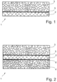
- FIG. 1 a schematic representation of an embodiment of a copper-ceramic substrate 1 with a ceramic carrier 2 and a proposed copper layer 3 is shown.
- the copper layer 3 has a high copper content of at least 99.5% Cu, with a silver content of at least 50 ppm Ag and a maximum of 3000 ppm Ag being provided.
- the copper layer 3 can be connected to the ceramic carrier 2, for example, using the DCB method described above or using the AMB method, so that it is connected to the ceramic carrier 2 by a material-locking connection in the surface edge zone 5.
- FIG 2 is a schematic representation of an embodiment of a copper-ceramic substrate 1 with a ceramic carrier 2 analogous to the embodiment of the Figure 1 shown, whereby two proposed copper layers 3 and 4 are provided.
- the copper layers 3 and 4 have a high copper content of at least 99.5% Cu, whereby a silver content of at least 50 ppm Ag and a maximum of 3000 ppm Ag is provided.
- the copper layers 3 and 4 can be connected to the ceramic carrier 2, for example, using the DCB method described above or using the AMB method, so that they can be connected by a materially bonded to the ceramic carrier 2 in the respective surface edge zones 5 and 6.
- the copper layers 3 and 4 with the proposed Cu and Ag proportions are highly conductive Cu materials and have a conductivity of 55 MS/m, preferably at least 57 MS/m and particularly preferably at least 58 MS/m.
- the limitation of the phosphorus content to a maximum of 30 ppm P and the presence of other elements in the copper layers 3, 4 means that the comparatively small proportions of Ag are sufficient to counteract a coarsening of the structure of the copper layers 3, 4 due to the thermal influence in the AMB process or DCB process, so that the copper layers 3, 4 of the copper-ceramic substrate 1 have a fine and homogeneous structure. This is particularly suitable for etching the finest structures, for example. Furthermore, the fine structure increases the strength of the copper layers 3, 4 and thus increases their resistance to mechanical damage in accordance with the Hall-patch relationship.
- the copper semi-finished products of the copper layers 3 and 4 can have a thickness of 0.1 to 1.0 mm and are placed in large dimensions on the ceramic carrier 2 and connected to the ceramic carrier 2 using the DCB process.
- the large-area copper-ceramic substrate 1 is then cut into smaller units and further processed.
- the connection can be made using the AMB process.
- Such copper semi-finished products for the copper layers 3, 4 can be manufactured, for example, in manufacturing processes under oxygen exclusion.
- the copper layers 3 and 4 can have a proportion of the elements Cd, Ce, Ge, V, Zn of a minimum of 0.01 to a maximum of 1 ppm each and/or a proportion of the elements Bi, Se, Sn, Te of a minimum of 0.01 to a maximum of 2 ppm each and/or a proportion of the elements Al, Sb, Ti, Zr of a minimum of 0.01 to a maximum of 3 ppm each and/or a proportion of the elements As, Co, In, Mn, Pb, Si of a minimum of 0.01 to a maximum of 5 ppm each and/or a proportion of the elements B, Be, Cr, Fe, Mn, Ni, S of a minimum of 0.01 to a maximum of 10 ppm each.
- the additional elements listed can be deliberately introduced into the structure by doping during the melting process immediately before casting or can already be present in the copper layers 3 and 4 due to impurities during the production of the copper semi-finished products. In any case, the proportion of these elements, including other impurities, should preferably not exceed 50 ppm.
- the copper layers 3, 4 can have a proportion of the elements Cd, Ce, Ge, V, Zn of a total of at least 0.05 ppm and a maximum of 5 ppm, a proportion of the elements Bi, Se, Sn, Te of a total of at least 0.1 ppm and a maximum of 8 ppm, a proportion of the elements Al, Sb, Ti, Zr of a total of at least 0.1 ppm and a maximum of 10 ppm, a proportion of the elements As, Co, In, Mn, Pb, Si of a total of at least 0.1 ppm and a maximum of 20 ppm and a proportion of the elements B, Be, Cr, Fe, Mn, Ni, S of a total of at least 0.1 ppm and a maximum of 50 ppm.
- the described proportions of the elements can help to achieve the suggested average grain size of the structure.
- the structure formation is particularly due to the grain refinement of the structure caused by the elements and to the reduction of secondary recrystallization in the structure during the bonding process.
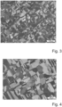
- FIG 3 a micrograph of one of the copper layers 3, 4 of the copper-ceramic substrate 1 is shown, which was produced using a DCB process.
- the structure of the copper layers 3, 4 in this embodiment is characterized by an average grain size of 56.5 ⁇ m with a standard deviation of 28.5 ⁇ m and is therefore below the requirements of 100 ⁇ m average grain size.
- the grain sizes were determined according to the line cutting method (DIN EN ISO 2624).
- FIG 4 a micrograph of one of the copper layers 3, 4 of the copper-ceramic substrate 1 is shown, which was produced using an AMB process.
- the structure of the copper layers 3, 4 in this embodiment is characterized by an average grain size of 78 ⁇ m with a standard deviation of 34.6 ⁇ m and is therefore below the requirements of 100 ⁇ m average grain size.
- the grain sizes were determined according to the line cutting method (DIN EN ISO 2624).
- FIG 6 are indentation hardnesses in GPa over a normal displacement in ⁇ m of a nanohardness measurement using depth-resolved QCSM method for a copper layer 3, 4 applied according to the DCB method (black circles), according to the AMB method (white circles) and a reference copper layer (black squares).
- the nanohardness measurements were carried out with several load levels, with the maximum test force being 100 mN.
- a Berkovich indenter was used as the indenter.
- the penetration hardness is accordingly applied depending on the penetration depth.
- the surfaces of the copper layers 3, 4 of the copper-ceramic substrates 1 according to the invention show a higher penetration hardness over all penetration depths up to 3.5 ⁇ m than the reference copper using both production methods.
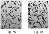
- the structures of the copper layers 3, 4 of the copper-ceramic substrate 1 according to the invention produced by the DCB process as well as by the AMB process are characterized by an increased formation of twins. Twins can be recognized in the micrograph as stripes that correspond to the middle area of a grain folded into the twin position.
- the structure can change depending on the selected production method, for example DCB ( Figure 7a ) or AMB ( Figure 7b ), of the copper-ceramic substrate 1 may differ slightly.
- Twinning is a known phenomenon in copper materials.
- the increased twinning is observed in the thermally activated joining process.
- Thermal twinning therefore occurs in the recrystallization process.
- This is thermally induced twinning (annealing twins).
- Twinning has a positive influence on the hardness of the material, particularly in the case of a fine structure.
- the twins are in the Figure 7 dark colored. According to the Figure 7a
- the area proportion of the twins is 19.4%.
- the copper layer 3, 4 according to the AMB process according to the embodiment of the Figure 7b This results in a surface area of twins of 21.6%.
- the surface areas mentioned differ only slightly from a reference copper, there are more smaller twins, which has a greater effect on the increase in hardness than a smaller number of large twins.
Landscapes
- Chemical & Material Sciences (AREA)
- Engineering & Computer Science (AREA)
- Ceramic Engineering (AREA)
- Materials Engineering (AREA)
- Structural Engineering (AREA)
- Organic Chemistry (AREA)
- Parts Printed On Printed Circuit Boards (AREA)
- Ceramic Products (AREA)
- Laminated Bodies (AREA)
Claims (8)
- Substrat en cuivre-céramique (1) comportant- un support de céramique (2) et- au moins une couche de cuivre (3, 4) reliée avec une surface du support de céramique (2),
caractérisé en ce que- la couche de cuivre (3, 4) présente une quantité d'au moins 99,5 % de Cu,- la couche de cuivre (3, 4) présente une quantité d'au moins 50 ppm d'Ag, et- la couche de cuivre (3, 4) présente une quantité d'au maximum 3000 ppm d'Ag, et- la couche de cuivre (3, 4) présente une quantité d'au maximum 30 ppm de P, et- la couche de cuivre (3, 4) présente une quantité d'au moins 0,1 ppm de P. Les quantités sont des quantités en poids. - Substrat en cuivre-céramique (1) selon la revendication 1, caractérisé en ce que la couche de cuivre (3, 4) présente une taille des grains moyenne entre 40 µm et 100 µm. Les tailles des grains ont été déterminées selon le la méthode de la moyenne des interceptions linéaires (DIN EN ISO 2624).
- Substrat en cuivre-céramique (1) selon la revendication 2, caractérisé en ce que la couche de cuivre (3, 4) présente une taille des grains moyenne entre 40 µm et 80 µm.
- Substrat en cuivre-céramique (1) selon l'une quelconque des revendications précédentes, caractérisé en ce que la couche de cuivre (3, 4) présente une dureté à la pénétration d'au moins 0,7 GPa pour des profondeurs de pénétration entre 0,4 µm à 0,6 µm.
- Substrat en cuivre-céramique (1) selon l'une quelconque des revendications précédentes, caractérisé en ce que la couche de cuivre (3. 4) présente une dureté à la pénétration d'au moins 0,8 GPa pour des profondeurs de pénétration entre 0,1 µm et 0,25 µm.
La mesure de la dureté nanométrique a été effectuée au moyen de la méthode code de spécialité commune, QCSM, basée sur la profondeur de pénétration. La mesure de la dureté nanométrique a été effectuée avec plusieurs niveaux de charge, où la charge d'essai maximale était de100 mN. On a utilisé le pénétrateur de Berkovich en tant qu'indenteur. - Substrat en cuivre-céramique (1) selon l'une quelconque des revendications précédentes, caractérisé en ce que- la couche de cuivre (3, 4) présente une quantité d'au maximum 10 ppm d'O.
- Substrat en cuivre-céramique (1) selon l'une quelconque des revendications précédentes, caractérisé en ce que- la couche de cuivre (3, 4) présente une quantité d'au moins 0,1 ppm d'O.
- Substrat en cuivre-céramique (1) selon l'une quelconque des revendications précédentes, caractérisé en ce que la couche de cuivre (3, 4) présente une quantité des éléments Cd, Ce, Ge, V, Zn, Bi, Se, Sn, Te, Al, Sb, Ti, Zr, As, Co, In, Mn, Pb, Si, B, Be, Cr, Fe, Mn, Ni, S, y compris d'autres impuretés, d'au maximum 50 ppm.
Applications Claiming Priority (2)
| Application Number | Priority Date | Filing Date | Title |
|---|---|---|---|
| DE102020213729.3A DE102020213729A1 (de) | 2020-11-02 | 2020-11-02 | Kupfer-Keramik-Substrat |
| PCT/EP2021/080163 WO2022090487A1 (fr) | 2020-11-02 | 2021-10-29 | Substrat en cuivre-céramique |
Publications (2)
| Publication Number | Publication Date |
|---|---|
| EP4237390A1 EP4237390A1 (fr) | 2023-09-06 |
| EP4237390B1 true EP4237390B1 (fr) | 2024-12-04 |
Family
ID=78536178
Family Applications (1)
| Application Number | Title | Priority Date | Filing Date |
|---|---|---|---|
| EP21805423.7A Active EP4237390B1 (fr) | 2020-11-02 | 2021-10-29 | Substrat en cuivre-céramique |
Country Status (9)
| Country | Link |
|---|---|
| US (1) | US20230399267A1 (fr) |
| EP (1) | EP4237390B1 (fr) |
| JP (1) | JP2023551759A (fr) |
| KR (1) | KR20230098154A (fr) |
| CN (1) | CN116390897A (fr) |
| DE (1) | DE102020213729A1 (fr) |
| ES (1) | ES3010057T3 (fr) |
| HU (1) | HUE070801T2 (fr) |
| WO (1) | WO2022090487A1 (fr) |
Families Citing this family (2)
| Publication number | Priority date | Publication date | Assignee | Title |
|---|---|---|---|---|
| CN118373699B (zh) * | 2024-04-24 | 2024-11-29 | 江苏富乐华半导体科技股份有限公司 | 一种dcb覆铜陶瓷载板生产的方法 |
| TWI893845B (zh) * | 2024-06-13 | 2025-08-11 | 聖崴科技股份有限公司 | 封裝結構及其形成方法 |
Citations (1)
| Publication number | Priority date | Publication date | Assignee | Title |
|---|---|---|---|---|
| JP2003096526A (ja) * | 2001-07-17 | 2003-04-03 | Nippon Mining & Metals Co Ltd | 銅張積層板用圧延銅箔およびその製造方法 |
Family Cites Families (15)
| Publication number | Priority date | Publication date | Assignee | Title |
|---|---|---|---|---|
| JP3856581B2 (ja) * | 1999-01-18 | 2006-12-13 | 日鉱金属株式会社 | フレキシブルプリント回路基板用圧延銅箔およびその製造方法 |
| JP2000328159A (ja) * | 1999-05-19 | 2000-11-28 | Kobe Steel Ltd | 銅合金箔 |
| JP2004263850A (ja) * | 2002-04-26 | 2004-09-24 | Nissan Motor Co Ltd | 摺動部材とその製造方法 |
| JP4915011B2 (ja) * | 2005-03-31 | 2012-04-11 | Dowaメタルテック株式会社 | 金属−セラミックス接合基板 |
| JP6425404B2 (ja) * | 2014-04-16 | 2018-11-21 | 株式会社Shカッパープロダクツ | セラミック配線基板用銅合金材、セラミック配線基板及びセラミック配線基板の製造方法 |
| JP6867102B2 (ja) * | 2014-10-22 | 2021-04-28 | Jx金属株式会社 | 銅放熱材、キャリア付銅箔、コネクタ、端子、積層体、シールド材、プリント配線板、金属加工部材、電子機器、及び、プリント配線板の製造方法 |
| JP2016179491A (ja) * | 2015-03-24 | 2016-10-13 | 関東冶金工業株式会社 | 多孔質金属部材の被覆接合方法、被覆接合部材、およびヒートシンク |
| DE102015224464A1 (de) * | 2015-12-07 | 2017-06-08 | Aurubis Stolberg Gmbh & Co. Kg | Kupfer-Keramik-Substrat, Kupferhalbzeug zur Herstellung eines Kupfer-Keramik-Substrats und Verfahren zur Herstellung eines Kupfer-Keramik-Substrats |
| JP6392268B2 (ja) * | 2016-02-05 | 2018-09-19 | Jx金属株式会社 | フレキシブルプリント基板用銅箔、それを用いた銅張積層体、フレキシブルプリント基板、及び電子機器 |
| JP6781562B2 (ja) * | 2016-03-28 | 2020-11-04 | Jx金属株式会社 | フレキシブルプリント基板用銅箔、それを用いた銅張積層体、フレキシブルプリント基板、及び電子機器 |
| JP6612168B2 (ja) * | 2016-03-30 | 2019-11-27 | Jx金属株式会社 | 銅箔、銅張積層板、並びにフレキシブルプリント基板及び電子機器 |
| EP3768654B1 (fr) | 2018-03-20 | 2022-04-20 | Aurubis Stolberg GmbH & Co. KG | Substrat cuivre-céramique |
| JP6572998B1 (ja) * | 2018-06-12 | 2019-09-11 | 千住金属工業株式会社 | Cu核ボール、はんだ継手、はんだペースト及びフォームはんだ |
| JP7212700B2 (ja) * | 2018-12-28 | 2023-01-25 | デンカ株式会社 | セラミックス-銅複合体、セラミックス回路基板、パワーモジュール及びセラミックス-銅複合体の製造方法 |
| KR20210123305A (ko) * | 2019-02-04 | 2021-10-13 | 미쓰비시 마테리알 가부시키가이샤 | 구리/세라믹스 접합체의 제조 방법, 절연 회로 기판의 제조 방법, 구리/세라믹스 접합체, 및 절연 회로 기판 |
-
2020
- 2020-11-02 DE DE102020213729.3A patent/DE102020213729A1/de not_active Ceased
-
2021
- 2021-10-29 CN CN202180066263.0A patent/CN116390897A/zh active Pending
- 2021-10-29 KR KR1020237012333A patent/KR20230098154A/ko active Pending
- 2021-10-29 WO PCT/EP2021/080163 patent/WO2022090487A1/fr not_active Ceased
- 2021-10-29 ES ES21805423T patent/ES3010057T3/es active Active
- 2021-10-29 EP EP21805423.7A patent/EP4237390B1/fr active Active
- 2021-10-29 JP JP2023518531A patent/JP2023551759A/ja active Pending
- 2021-10-29 US US18/033,573 patent/US20230399267A1/en not_active Abandoned
- 2021-10-29 HU HUE21805423A patent/HUE070801T2/hu unknown
Patent Citations (1)
| Publication number | Priority date | Publication date | Assignee | Title |
|---|---|---|---|---|
| JP2003096526A (ja) * | 2001-07-17 | 2003-04-03 | Nippon Mining & Metals Co Ltd | 銅張積層板用圧延銅箔およびその製造方法 |
Also Published As
| Publication number | Publication date |
|---|---|
| KR20230098154A (ko) | 2023-07-03 |
| US20230399267A1 (en) | 2023-12-14 |
| ES3010057T3 (en) | 2025-04-01 |
| DE102020213729A1 (de) | 2022-05-05 |
| JP2023551759A (ja) | 2023-12-13 |
| HUE070801T2 (hu) | 2025-07-28 |
| WO2022090487A1 (fr) | 2022-05-05 |
| CN116390897A (zh) | 2023-07-04 |
| EP4237390A1 (fr) | 2023-09-06 |
Similar Documents
| Publication | Publication Date | Title |
|---|---|---|
| EP3386934B1 (fr) | Substrat en cuivre-céramique, produit semi-fini en cuivre pour la fabrication d'un substrat en cuivre-céramique et procédé pour la fabrication d'un substrat en cuivre-céramique | |
| DE102020111700B4 (de) | Trägersubstrat und Verfahren zur Herstellung eines Trägersubstrats | |
| DE19961537B4 (de) | Verfahren zur Herstellung einer Glaskeramiktafel | |
| DE112017000184T5 (de) | Lotverbindung | |
| DE102009015520A1 (de) | Metall-Keramik-Substrat | |
| EP4237390B1 (fr) | Substrat en cuivre-céramique | |
| EP4037867B1 (fr) | Matériau de soudure, procédé de fabrication d'un tel matériau de soudure et utilisation d'un tel matériau de soudure pour relier une couche métallique à une couche céramique | |
| DE102019135099A1 (de) | Verfahren zur Herstellung eines Metall-Keramik-Substrats und Metall-Keramik-Substrat, hergestellt mit einem solchen Verfahren | |
| EP3419950B1 (fr) | Composite cuivre-ceramique | |
| DE102005042554A1 (de) | Metall-Keramik-Substrat | |
| EP3717236B1 (fr) | Procédé de fabrication d'un substrat métal-céramique | |
| DE102017128308B4 (de) | Verfahren zur Herstellung eines Metall-Keramik-Substrats | |
| EP3419949B1 (fr) | Composite en ceramique/cuivre | |
| EP3419952B1 (fr) | Composite cuivre-ceramique | |
| EP3210951B9 (fr) | Composite en ceramique/cuivre | |
| EP3210956B1 (fr) | Composite en ceramique/cuivre | |
| EP3768654B1 (fr) | Substrat cuivre-céramique | |
| EP3419951B1 (fr) | Composite cuivre-ceramique | |
| DE102020120188B4 (de) | Verfahren zur Herstellung eines Trägersubstrats und ein Trägersubstrat hergestellt mit einem solchen Verfahren | |
| EP4325227A1 (fr) | Matière composite en forme de ruban pour aiguilles de contrôle | |
| EP3210957B1 (fr) | Composite en ceramique/cuivre | |
| DE102020215574A1 (de) | Hochtemperaturfähiger und thermoschockbeständiger hartgelöteter artikel | |
| EP4644351A2 (fr) | Procédé de fabrication d'un substrat métal-céramique, élément céramique et couche métallique pour un tel procédé et substrat métal-céramique fabriqué par un tel procédé | |
| DE102023103850A1 (de) | Metall-Keramik-Substrat und Verfahren zur Herstellung eines Metall-Keramik-Substrats | |
| EP4311818A1 (fr) | Substrat métallique céramique pourvu de zone de contact |
Legal Events
| Date | Code | Title | Description |
|---|---|---|---|
| STAA | Information on the status of an ep patent application or granted ep patent |
Free format text: STATUS: UNKNOWN |
|
| STAA | Information on the status of an ep patent application or granted ep patent |
Free format text: STATUS: THE INTERNATIONAL PUBLICATION HAS BEEN MADE |
|
| PUAI | Public reference made under article 153(3) epc to a published international application that has entered the european phase |
Free format text: ORIGINAL CODE: 0009012 |
|
| STAA | Information on the status of an ep patent application or granted ep patent |
Free format text: STATUS: REQUEST FOR EXAMINATION WAS MADE |
|
| 17P | Request for examination filed |
Effective date: 20230601 |
|
| AK | Designated contracting states |
Kind code of ref document: A1 Designated state(s): AL AT BE BG CH CY CZ DE DK EE ES FI FR GB GR HR HU IE IS IT LI LT LU LV MC MK MT NL NO PL PT RO RS SE SI SK SM TR |
|
| DAV | Request for validation of the european patent (deleted) | ||
| DAX | Request for extension of the european patent (deleted) | ||
| GRAP | Despatch of communication of intention to grant a patent |
Free format text: ORIGINAL CODE: EPIDOSNIGR1 |
|
| STAA | Information on the status of an ep patent application or granted ep patent |
Free format text: STATUS: GRANT OF PATENT IS INTENDED |
|
| INTG | Intention to grant announced |
Effective date: 20240627 |
|
| GRAS | Grant fee paid |
Free format text: ORIGINAL CODE: EPIDOSNIGR3 |
|
| GRAA | (expected) grant |
Free format text: ORIGINAL CODE: 0009210 |
|
| STAA | Information on the status of an ep patent application or granted ep patent |
Free format text: STATUS: THE PATENT HAS BEEN GRANTED |
|
| AK | Designated contracting states |
Kind code of ref document: B1 Designated state(s): AL AT BE BG CH CY CZ DE DK EE ES FI FR GB GR HR HU IE IS IT LI LT LU LV MC MK MT NL NO PL PT RO RS SE SI SK SM TR |
|
| REG | Reference to a national code |
Ref country code: CH Ref legal event code: EP |
|
| REG | Reference to a national code |
Ref country code: DE Ref legal event code: R096 Ref document number: 502021006042 Country of ref document: DE |
|
| REG | Reference to a national code |
Ref country code: IE Ref legal event code: FG4D Free format text: LANGUAGE OF EP DOCUMENT: GERMAN |
|
| REG | Reference to a national code |
Ref country code: SE Ref legal event code: TRGR |
|
| REG | Reference to a national code |
Ref country code: LT Ref legal event code: MG9D |
|
| REG | Reference to a national code |
Ref country code: ES Ref legal event code: FG2A Ref document number: 3010057 Country of ref document: ES Kind code of ref document: T3 Effective date: 20250401 |
|
| REG | Reference to a national code |
Ref country code: NL Ref legal event code: MP Effective date: 20241204 |
|
| PG25 | Lapsed in a contracting state [announced via postgrant information from national office to epo] |
Ref country code: HR Free format text: LAPSE BECAUSE OF FAILURE TO SUBMIT A TRANSLATION OF THE DESCRIPTION OR TO PAY THE FEE WITHIN THE PRESCRIBED TIME-LIMIT Effective date: 20241204 |
|
| PG25 | Lapsed in a contracting state [announced via postgrant information from national office to epo] |
Ref country code: FI Free format text: LAPSE BECAUSE OF FAILURE TO SUBMIT A TRANSLATION OF THE DESCRIPTION OR TO PAY THE FEE WITHIN THE PRESCRIBED TIME-LIMIT Effective date: 20241204 |
|
| PG25 | Lapsed in a contracting state [announced via postgrant information from national office to epo] |
Ref country code: BG Free format text: LAPSE BECAUSE OF FAILURE TO SUBMIT A TRANSLATION OF THE DESCRIPTION OR TO PAY THE FEE WITHIN THE PRESCRIBED TIME-LIMIT Effective date: 20241204 |
|
| PG25 | Lapsed in a contracting state [announced via postgrant information from national office to epo] |
Ref country code: NO Free format text: LAPSE BECAUSE OF FAILURE TO SUBMIT A TRANSLATION OF THE DESCRIPTION OR TO PAY THE FEE WITHIN THE PRESCRIBED TIME-LIMIT Effective date: 20250304 |
|
| PG25 | Lapsed in a contracting state [announced via postgrant information from national office to epo] |
Ref country code: LV Free format text: LAPSE BECAUSE OF FAILURE TO SUBMIT A TRANSLATION OF THE DESCRIPTION OR TO PAY THE FEE WITHIN THE PRESCRIBED TIME-LIMIT Effective date: 20241204 Ref country code: GR Free format text: LAPSE BECAUSE OF FAILURE TO SUBMIT A TRANSLATION OF THE DESCRIPTION OR TO PAY THE FEE WITHIN THE PRESCRIBED TIME-LIMIT Effective date: 20250305 |
|
| PG25 | Lapsed in a contracting state [announced via postgrant information from national office to epo] |
Ref country code: RS Free format text: LAPSE BECAUSE OF FAILURE TO SUBMIT A TRANSLATION OF THE DESCRIPTION OR TO PAY THE FEE WITHIN THE PRESCRIBED TIME-LIMIT Effective date: 20250304 |
|
| PG25 | Lapsed in a contracting state [announced via postgrant information from national office to epo] |
Ref country code: NL Free format text: LAPSE BECAUSE OF FAILURE TO SUBMIT A TRANSLATION OF THE DESCRIPTION OR TO PAY THE FEE WITHIN THE PRESCRIBED TIME-LIMIT Effective date: 20241204 |
|
| PG25 | Lapsed in a contracting state [announced via postgrant information from national office to epo] |
Ref country code: SM Free format text: LAPSE BECAUSE OF FAILURE TO SUBMIT A TRANSLATION OF THE DESCRIPTION OR TO PAY THE FEE WITHIN THE PRESCRIBED TIME-LIMIT Effective date: 20241204 |
|
| PG25 | Lapsed in a contracting state [announced via postgrant information from national office to epo] |
Ref country code: PL Free format text: LAPSE BECAUSE OF FAILURE TO SUBMIT A TRANSLATION OF THE DESCRIPTION OR TO PAY THE FEE WITHIN THE PRESCRIBED TIME-LIMIT Effective date: 20241204 |
|
| PG25 | Lapsed in a contracting state [announced via postgrant information from national office to epo] |
Ref country code: IS Free format text: LAPSE BECAUSE OF FAILURE TO SUBMIT A TRANSLATION OF THE DESCRIPTION OR TO PAY THE FEE WITHIN THE PRESCRIBED TIME-LIMIT Effective date: 20250404 |
|
| PG25 | Lapsed in a contracting state [announced via postgrant information from national office to epo] |
Ref country code: PT Free format text: LAPSE BECAUSE OF FAILURE TO SUBMIT A TRANSLATION OF THE DESCRIPTION OR TO PAY THE FEE WITHIN THE PRESCRIBED TIME-LIMIT Effective date: 20250404 |
|
| PG25 | Lapsed in a contracting state [announced via postgrant information from national office to epo] |
Ref country code: EE Free format text: LAPSE BECAUSE OF FAILURE TO SUBMIT A TRANSLATION OF THE DESCRIPTION OR TO PAY THE FEE WITHIN THE PRESCRIBED TIME-LIMIT Effective date: 20241204 |
|
| PG25 | Lapsed in a contracting state [announced via postgrant information from national office to epo] |
Ref country code: SK Free format text: LAPSE BECAUSE OF FAILURE TO SUBMIT A TRANSLATION OF THE DESCRIPTION OR TO PAY THE FEE WITHIN THE PRESCRIBED TIME-LIMIT Effective date: 20241204 |
|
| PG25 | Lapsed in a contracting state [announced via postgrant information from national office to epo] |
Ref country code: CZ Free format text: LAPSE BECAUSE OF FAILURE TO SUBMIT A TRANSLATION OF THE DESCRIPTION OR TO PAY THE FEE WITHIN THE PRESCRIBED TIME-LIMIT Effective date: 20241204 |
|
| REG | Reference to a national code |
Ref country code: HU Ref legal event code: AG4A Ref document number: E070801 Country of ref document: HU |
|
| REG | Reference to a national code |
Ref country code: DE Ref legal event code: R097 Ref document number: 502021006042 Country of ref document: DE |
|
| PG25 | Lapsed in a contracting state [announced via postgrant information from national office to epo] |
Ref country code: DK Free format text: LAPSE BECAUSE OF FAILURE TO SUBMIT A TRANSLATION OF THE DESCRIPTION OR TO PAY THE FEE WITHIN THE PRESCRIBED TIME-LIMIT Effective date: 20241204 |
|
| PLBE | No opposition filed within time limit |
Free format text: ORIGINAL CODE: 0009261 |
|
| STAA | Information on the status of an ep patent application or granted ep patent |
Free format text: STATUS: NO OPPOSITION FILED WITHIN TIME LIMIT |
|
| 26N | No opposition filed |
Effective date: 20250905 |
|
| PGFP | Annual fee paid to national office [announced via postgrant information from national office to epo] |
Ref country code: HU Payment date: 20251029 Year of fee payment: 5 |
|
| PGFP | Annual fee paid to national office [announced via postgrant information from national office to epo] |
Ref country code: DE Payment date: 20251020 Year of fee payment: 5 |
|
| PGFP | Annual fee paid to national office [announced via postgrant information from national office to epo] |
Ref country code: GB Payment date: 20251024 Year of fee payment: 5 |
|
| PGFP | Annual fee paid to national office [announced via postgrant information from national office to epo] |
Ref country code: AT Payment date: 20260113 Year of fee payment: 5 |
|
| PGFP | Annual fee paid to national office [announced via postgrant information from national office to epo] |
Ref country code: IT Payment date: 20251031 Year of fee payment: 5 |
|
| PGFP | Annual fee paid to national office [announced via postgrant information from national office to epo] |
Ref country code: FR Payment date: 20251027 Year of fee payment: 5 |
|
| PGFP | Annual fee paid to national office [announced via postgrant information from national office to epo] |
Ref country code: SE Payment date: 20251023 Year of fee payment: 5 |
|
| PGFP | Annual fee paid to national office [announced via postgrant information from national office to epo] |
Ref country code: RO Payment date: 20251028 Year of fee payment: 5 |
|
| PGFP | Annual fee paid to national office [announced via postgrant information from national office to epo] |
Ref country code: ES Payment date: 20251114 Year of fee payment: 5 |