EP3214637A1 - Appareil de traitement de plasma - Google Patents
Appareil de traitement de plasma Download PDFInfo
- Publication number
- EP3214637A1 EP3214637A1 EP17158675.3A EP17158675A EP3214637A1 EP 3214637 A1 EP3214637 A1 EP 3214637A1 EP 17158675 A EP17158675 A EP 17158675A EP 3214637 A1 EP3214637 A1 EP 3214637A1
- Authority
- EP
- European Patent Office
- Prior art keywords
- electrode structure
- chamber
- inductively coupled
- plasma processing
- substrate
- Prior art date
- Legal status (The legal status is an assumption and is not a legal conclusion. Google has not performed a legal analysis and makes no representation as to the accuracy of the status listed.)
- Granted
Links
Images


Classifications
-
- H—ELECTRICITY
- H01—ELECTRIC ELEMENTS
- H01J—ELECTRIC DISCHARGE TUBES OR DISCHARGE LAMPS
- H01J37/00—Discharge tubes with provision for introducing objects or material to be exposed to the discharge, e.g. for the purpose of examination or processing thereof
- H01J37/32—Gas-filled discharge tubes
- H01J37/32431—Constructional details of the reactor
- H01J37/32532—Electrodes
- H01J37/32568—Relative arrangement or disposition of electrodes; moving means
-
- H—ELECTRICITY
- H01—ELECTRIC ELEMENTS
- H01J—ELECTRIC DISCHARGE TUBES OR DISCHARGE LAMPS
- H01J37/00—Discharge tubes with provision for introducing objects or material to be exposed to the discharge, e.g. for the purpose of examination or processing thereof
- H01J37/32—Gas-filled discharge tubes
- H01J37/32431—Constructional details of the reactor
- H01J37/32458—Vessel
- H01J37/32467—Material
-
- B—PERFORMING OPERATIONS; TRANSPORTING
- B08—CLEANING
- B08B—CLEANING IN GENERAL; PREVENTION OF FOULING IN GENERAL
- B08B7/00—Cleaning by methods not provided for in a single other subclass or a single group in this subclass
- B08B7/0035—Cleaning by methods not provided for in a single other subclass or a single group in this subclass by radiant energy, e.g. UV, laser, light beam or the like
-
- B—PERFORMING OPERATIONS; TRANSPORTING
- B08—CLEANING
- B08B—CLEANING IN GENERAL; PREVENTION OF FOULING IN GENERAL
- B08B9/00—Cleaning hollow articles by methods or apparatus specially adapted thereto
- B08B9/08—Cleaning containers, e.g. tanks
-
- C—CHEMISTRY; METALLURGY
- C23—COATING METALLIC MATERIAL; COATING MATERIAL WITH METALLIC MATERIAL; CHEMICAL SURFACE TREATMENT; DIFFUSION TREATMENT OF METALLIC MATERIAL; COATING BY VACUUM EVAPORATION, BY SPUTTERING, BY ION IMPLANTATION OR BY CHEMICAL VAPOUR DEPOSITION, IN GENERAL; INHIBITING CORROSION OF METALLIC MATERIAL OR INCRUSTATION IN GENERAL
- C23C—COATING METALLIC MATERIAL; COATING MATERIAL WITH METALLIC MATERIAL; SURFACE TREATMENT OF METALLIC MATERIAL BY DIFFUSION INTO THE SURFACE, BY CHEMICAL CONVERSION OR SUBSTITUTION; COATING BY VACUUM EVAPORATION, BY SPUTTERING, BY ION IMPLANTATION OR BY CHEMICAL VAPOUR DEPOSITION, IN GENERAL
- C23C16/00—Chemical coating by decomposition of gaseous compounds, without leaving reaction products of surface material in the coating, i.e. chemical vapour deposition [CVD] processes
- C23C16/44—Chemical coating by decomposition of gaseous compounds, without leaving reaction products of surface material in the coating, i.e. chemical vapour deposition [CVD] processes characterised by the method of coating
- C23C16/4401—Means for minimising impurities, e.g. dust, moisture or residual gas, in the reaction chamber
- C23C16/4405—Cleaning of reactor or parts inside the reactor by using reactive gases
-
- C—CHEMISTRY; METALLURGY
- C23—COATING METALLIC MATERIAL; COATING MATERIAL WITH METALLIC MATERIAL; CHEMICAL SURFACE TREATMENT; DIFFUSION TREATMENT OF METALLIC MATERIAL; COATING BY VACUUM EVAPORATION, BY SPUTTERING, BY ION IMPLANTATION OR BY CHEMICAL VAPOUR DEPOSITION, IN GENERAL; INHIBITING CORROSION OF METALLIC MATERIAL OR INCRUSTATION IN GENERAL
- C23C—COATING METALLIC MATERIAL; COATING MATERIAL WITH METALLIC MATERIAL; SURFACE TREATMENT OF METALLIC MATERIAL BY DIFFUSION INTO THE SURFACE, BY CHEMICAL CONVERSION OR SUBSTITUTION; COATING BY VACUUM EVAPORATION, BY SPUTTERING, BY ION IMPLANTATION OR BY CHEMICAL VAPOUR DEPOSITION, IN GENERAL
- C23C16/00—Chemical coating by decomposition of gaseous compounds, without leaving reaction products of surface material in the coating, i.e. chemical vapour deposition [CVD] processes
- C23C16/44—Chemical coating by decomposition of gaseous compounds, without leaving reaction products of surface material in the coating, i.e. chemical vapour deposition [CVD] processes characterised by the method of coating
- C23C16/448—Chemical coating by decomposition of gaseous compounds, without leaving reaction products of surface material in the coating, i.e. chemical vapour deposition [CVD] processes characterised by the method of coating characterised by the method used for generating reactive gas streams, e.g. by evaporation or sublimation of precursor materials
-
- C—CHEMISTRY; METALLURGY
- C23—COATING METALLIC MATERIAL; COATING MATERIAL WITH METALLIC MATERIAL; CHEMICAL SURFACE TREATMENT; DIFFUSION TREATMENT OF METALLIC MATERIAL; COATING BY VACUUM EVAPORATION, BY SPUTTERING, BY ION IMPLANTATION OR BY CHEMICAL VAPOUR DEPOSITION, IN GENERAL; INHIBITING CORROSION OF METALLIC MATERIAL OR INCRUSTATION IN GENERAL
- C23C—COATING METALLIC MATERIAL; COATING MATERIAL WITH METALLIC MATERIAL; SURFACE TREATMENT OF METALLIC MATERIAL BY DIFFUSION INTO THE SURFACE, BY CHEMICAL CONVERSION OR SUBSTITUTION; COATING BY VACUUM EVAPORATION, BY SPUTTERING, BY ION IMPLANTATION OR BY CHEMICAL VAPOUR DEPOSITION, IN GENERAL
- C23C16/00—Chemical coating by decomposition of gaseous compounds, without leaving reaction products of surface material in the coating, i.e. chemical vapour deposition [CVD] processes
- C23C16/44—Chemical coating by decomposition of gaseous compounds, without leaving reaction products of surface material in the coating, i.e. chemical vapour deposition [CVD] processes characterised by the method of coating
- C23C16/50—Chemical coating by decomposition of gaseous compounds, without leaving reaction products of surface material in the coating, i.e. chemical vapour deposition [CVD] processes characterised by the method of coating using electric discharges
- C23C16/503—Chemical coating by decomposition of gaseous compounds, without leaving reaction products of surface material in the coating, i.e. chemical vapour deposition [CVD] processes characterised by the method of coating using electric discharges using DC or AC discharges
-
- C—CHEMISTRY; METALLURGY
- C23—COATING METALLIC MATERIAL; COATING MATERIAL WITH METALLIC MATERIAL; CHEMICAL SURFACE TREATMENT; DIFFUSION TREATMENT OF METALLIC MATERIAL; COATING BY VACUUM EVAPORATION, BY SPUTTERING, BY ION IMPLANTATION OR BY CHEMICAL VAPOUR DEPOSITION, IN GENERAL; INHIBITING CORROSION OF METALLIC MATERIAL OR INCRUSTATION IN GENERAL
- C23C—COATING METALLIC MATERIAL; COATING MATERIAL WITH METALLIC MATERIAL; SURFACE TREATMENT OF METALLIC MATERIAL BY DIFFUSION INTO THE SURFACE, BY CHEMICAL CONVERSION OR SUBSTITUTION; COATING BY VACUUM EVAPORATION, BY SPUTTERING, BY ION IMPLANTATION OR BY CHEMICAL VAPOUR DEPOSITION, IN GENERAL
- C23C16/00—Chemical coating by decomposition of gaseous compounds, without leaving reaction products of surface material in the coating, i.e. chemical vapour deposition [CVD] processes
- C23C16/44—Chemical coating by decomposition of gaseous compounds, without leaving reaction products of surface material in the coating, i.e. chemical vapour deposition [CVD] processes characterised by the method of coating
- C23C16/50—Chemical coating by decomposition of gaseous compounds, without leaving reaction products of surface material in the coating, i.e. chemical vapour deposition [CVD] processes characterised by the method of coating using electric discharges
- C23C16/505—Chemical coating by decomposition of gaseous compounds, without leaving reaction products of surface material in the coating, i.e. chemical vapour deposition [CVD] processes characterised by the method of coating using electric discharges using radio frequency discharges
-
- H—ELECTRICITY
- H01—ELECTRIC ELEMENTS
- H01J—ELECTRIC DISCHARGE TUBES OR DISCHARGE LAMPS
- H01J37/00—Discharge tubes with provision for introducing objects or material to be exposed to the discharge, e.g. for the purpose of examination or processing thereof
- H01J37/32—Gas-filled discharge tubes
- H01J37/32009—Arrangements for generation of plasma specially adapted for examination or treatment of objects, e.g. plasma sources
- H01J37/32082—Radio frequency generated discharge
- H01J37/321—Radio frequency generated discharge the radio frequency energy being inductively coupled to the plasma
- H01J37/3211—Antennas, e.g. particular shapes of coils
-
- H—ELECTRICITY
- H01—ELECTRIC ELEMENTS
- H01J—ELECTRIC DISCHARGE TUBES OR DISCHARGE LAMPS
- H01J37/00—Discharge tubes with provision for introducing objects or material to be exposed to the discharge, e.g. for the purpose of examination or processing thereof
- H01J37/32—Gas-filled discharge tubes
- H01J37/32009—Arrangements for generation of plasma specially adapted for examination or treatment of objects, e.g. plasma sources
- H01J37/32082—Radio frequency generated discharge
- H01J37/32174—Circuits specially adapted for controlling the RF discharge
-
- H—ELECTRICITY
- H01—ELECTRIC ELEMENTS
- H01J—ELECTRIC DISCHARGE TUBES OR DISCHARGE LAMPS
- H01J37/00—Discharge tubes with provision for introducing objects or material to be exposed to the discharge, e.g. for the purpose of examination or processing thereof
- H01J37/32—Gas-filled discharge tubes
- H01J37/32431—Constructional details of the reactor
- H01J37/32532—Electrodes
- H01J37/32541—Shape
-
- H—ELECTRICITY
- H10—SEMICONDUCTOR DEVICES; ELECTRIC SOLID-STATE DEVICES NOT OTHERWISE PROVIDED FOR
- H10P—GENERIC PROCESSES OR APPARATUS FOR THE MANUFACTURE OR TREATMENT OF DEVICES COVERED BY CLASS H10
- H10P50/00—Etching of wafers, substrates or parts of devices
- H10P50/20—Dry etching; Plasma etching; Reactive-ion etching
- H10P50/24—Dry etching; Plasma etching; Reactive-ion etching of semiconductor materials
- H10P50/242—Dry etching; Plasma etching; Reactive-ion etching of semiconductor materials of Group IV materials
-
- H—ELECTRICITY
- H01—ELECTRIC ELEMENTS
- H01J—ELECTRIC DISCHARGE TUBES OR DISCHARGE LAMPS
- H01J2237/00—Discharge tubes exposing object to beam, e.g. for analysis treatment, etching, imaging
- H01J2237/32—Processing objects by plasma generation
- H01J2237/33—Processing objects by plasma generation characterised by the type of processing
- H01J2237/332—Coating
- H01J2237/3321—CVD [Chemical Vapor Deposition]
-
- H—ELECTRICITY
- H01—ELECTRIC ELEMENTS
- H01J—ELECTRIC DISCHARGE TUBES OR DISCHARGE LAMPS
- H01J2237/00—Discharge tubes exposing object to beam, e.g. for analysis treatment, etching, imaging
- H01J2237/32—Processing objects by plasma generation
- H01J2237/33—Processing objects by plasma generation characterised by the type of processing
- H01J2237/334—Etching
-
- H—ELECTRICITY
- H01—ELECTRIC ELEMENTS
- H01J—ELECTRIC DISCHARGE TUBES OR DISCHARGE LAMPS
- H01J2237/00—Discharge tubes exposing object to beam, e.g. for analysis treatment, etching, imaging
- H01J2237/32—Processing objects by plasma generation
- H01J2237/33—Processing objects by plasma generation characterised by the type of processing
- H01J2237/335—Cleaning
-
- H—ELECTRICITY
- H10—SEMICONDUCTOR DEVICES; ELECTRIC SOLID-STATE DEVICES NOT OTHERWISE PROVIDED FOR
- H10P—GENERIC PROCESSES OR APPARATUS FOR THE MANUFACTURE OR TREATMENT OF DEVICES COVERED BY CLASS H10
- H10P72/00—Handling or holding of wafers, substrates or devices during manufacture or treatment thereof
- H10P72/04—Apparatus for manufacture or treatment
- H10P72/0402—Apparatus for fluid treatment
- H10P72/0418—Apparatus for fluid treatment for etching
- H10P72/0421—Apparatus for fluid treatment for etching for drying etching
Definitions
- This invention relates to a plasma processing apparatus.
- the invention relates also to an associated method of plasma processing.
- ICP inductively coupled plasma
- RF power is applied to an externally positioned antenna, coil or band resulting in inductive coupling of energy into the process chamber through a dielectric container or window.
- a suitable gas or gaseous mixture is introduced into the process chamber at a relatively low pressure and a gas discharge is produced.
- Figures 1a and b show examples of prior art ICP designs.
- Figures 1a and b show a process chamber 10 having a dielectric cylindrical body, RF feed points 12, 14 and a tuning capacitor 20.
- Figure 1a shows a two turn ICP coil 16 which is externally positioned around the dielectric portion of the chamber 10.
- Figure 1b shows a single turn ICP coil externally positioned around the dielectric region of the chamber 10.
- the present invention in at least some of its embodiments, addresses the above mentioned problems and needs.
- a plasma processing apparatus for plasma processing a substrate comprising:
- the metallic electrode structure had the advantage of being relatively easy to cool. This can enable at least one of high power operation, high pressure operation, and high thermal loading to be achieved without requiring the use of a thermally robust dielectric chamber wall formed from an exotic material such as AlN.
- the electrode structure may be a single turn structure.
- the electrode structure may be a single non-continuous band forming a single turn around a periphery of the chamber.
- the electrode structure may comprise a plurality of spaced apart band segments.
- the band segments may form a single turn around a periphery of the chamber.
- the band segments may be spaced apart by portions of the chamber wall formed from a dielectric material.
- the band segments may be connected in parallel to the electrical signal supply device. This reduces the magnitude of the voltage that must be applied to each segment for operation of the apparatus. This assists in suppressing electric coupling around the feed points of the electrode structure.
- the electrode structure comprises two to six band segments.
- the band segments may be grounded at their midpoints. This can assist in minimizing sputtering or other undesirable affects associated with the applied electrical voltage.
- a lower region of the electrode structure may comprise one or more discontinuities which prevent the formation of a primary current flow in said lower region.
- the discontinuities may be slots formed in the electrode structure.
- the discontinuities may be filled with a dielectric material.
- the lower region of each band segment in the electrode array may comprise a discontinuity.
- the discontinuities can act break up the path of primary current flow. This forces the current to circulate only in the upper region of the electrode structure. As a result, the plasma can be confined to the upper region of the electrode structure.
- the metallic electrode structure is relatively easy to cool. This avoids undesirable heating of other areas of the apparatus which might be caused if the plasma were to extend beyond the electrode structure.
- the electrode structure may be a coil.
- the coil may be a single turn structure.
- the metallic material may be a metal such as aluminium.
- the electrode structure is in direct communication with the interior of the chamber. This reduces any transformer action leakage inductance since the primary winding (the electrode structure) is immediately adjacent to the secondary winding (the inductively coupled plasma). This leads to more efficient coupling. A further advantage is that it is possible to operate with a plasma over a wider range of power and pressure conditions.
- the electrode structure extends through at least one chamber wall from an outer surface to an inner surface thereof.
- the chamber may comprise a top portion, a body portion and a lower portion.
- the electrode structure may be located in the body portion.
- the body portion may be generally cylindrical.
- the body portion may comprise an upper section, a middle section and a lower section.
- the electrode structure may be located in the middle section.
- the upper and lower sections may be formed from a dielectric material.
- the apparatus may comprise a substrate support.
- the substrate support supports a substrate which is plasma processed by the apparatus.
- the substrate support may be positioned within the chamber. Alternatively, the substrate support may be positioned within a further chamber.
- the apparatus may further comprise a loading mechanism for loading the substrate onto the substrate support.
- the substrate support may be configured to receive a planar substrate such as a semiconductor wafer or a flat panel substrate.
- the remaining portion of the chamber wall or walls not constituted by the electrode structure is formed from one or more dielectric materials.
- Any suitable dielectric material such as a ceramic, alumina, or quartz, may be used.
- the apparatus may further comprise a cooling system for cooling the electrode structure.
- the cooling system may comprise channels formed in the electrode structure to permit a coolant fluid to be flowed therethrough. This is a very convenient way of achieving significant cooling of the electrode structure in a very straightforward manner.
- the apparatus may comprise a single chamber having the electrode structure or the apparatus may comprise multiple chambers.
- the apparatus may comprise a first chamber having the electrode structure which acts as a plasma source, and one of more further chambers in which plasma processing takes place.
- the apparatus may be configured as a source of one or both of ions and radicals which are used for the plasma processing.
- the electrical signal supply device may supply a RF electrical signal that drives the electrode structure.
- An additional electrical signal may be applied to the electrode structure in order to initially strike a plasma.
- the additional electrical signal may be a RF, AC or DC electrical signal.
- the additional electrical signal may be applied using an auxiliary electrical signal supply device. Additional electrical signal may be applied between source and ground.
- adjacent band segments can be powered using alternate polarities of the additional electrical signal.
- the RF electrical signal may be coupled by high pass filtering.
- a method of plasma processing a substrate comprising the steps of:
- the plasma processing may be performed to process a substrate which is positioned in the apparatus.
- the apparatus may comprise a substrate support.
- the method may comprise the step of loading the substrate onto the substrate support.
- a substrate support is present and the substrate may be positioned in the chamber in a different way.
- the plasma processing may form a feature or coating on the substrate.
- the substrate may be a semiconductor substrate.
- the semiconductor substrate may be a semiconductor wafer, such as a silicon wafer.
- the plasma processing may be a semiconductor processing technique.
- the substrate may be any substrate suitable for processing in this way.
- the semiconductor processing technique may process a semiconductor feature already present on the substrate or it may deposit a new feature onto to the substrate.
- the semiconductor processing technique may be an etch technique or a deposition technique such as Plasma enhanced chemical vapour deposition (PE-CVD).
- PE-CVD Plasma enhanced chemical vapour deposition
- a deposition technique may be used to deposit films of micron and sub-micron thickness.
- the substrate may be a flat panel, such as a LCD flat panel.
- the substrate may be formed from a metal or have a surface to be processed which is formed from a metal.
- the plasma processing may form a coating on the substrate.
- the coating may be a nitride coating.
- the substrate may be a tool part.
- the plasma processing may be a chamber cleaning process.
- the plasma processing may use one or both of ions and radicals which are produced in the plasma.
- the apparatus may comprise multiple chambers.
- the apparatus may comprise a first chamber having the electrode structure which acts as a plasma source, and one or more further chambers in which plasma processing takes place.
- the first chamber may provide a source of radicals.
- the plasma processing may be a radical based plasma process.
- the radicals may be F, N, 0 or any other suitable radical species.
- the plasma processing may be cleaning of a further chamber or processing of a substrate positioned in a further chamber. Processing of a substrate positioned in a further chamber may comprise a CVD process.
- the CVD process may be CVD epitaxy.
- FIG. 2 shows a first embodiment of a plasma processing apparatus of the invention, depicted generally at 100.
- the apparatus 100 comprises a chamber 102 having a suitable gas inlet 104 disposed in a top portion 102a thereof.
- the chamber 102 further comprises a generally cylindrical body 102b.
- the body 102b comprises an upper dielectric portion 102c, a lower dielectric portion, 102d and an electrode structure 102e which is positioned between the upper and lower dielectric sections 102c, d.
- the body portion 102b further comprises a base section 102f having a wafer loading slot 106 and a pumping port 108 which may be connected to a suitable pumping arrangement such as a vacuum line leading to a turbomolecular pump.
- the interior of the chamber 102 houses a platen 110 on which a substrate such as a wafer may be loaded.
- the platen 110 as shown in Figure 1 is in a lowered position for receiving the substrate.
- the platen 110 would then subsequently be raised into an elevated position prior to commencement of plasma processing.
- the platen 110 can be of any suitable form such as an electrostatic chuck. Other forms of clamping of the substrate, such as mechanical clamping, might be utilized as desired.
- an electrical bias signal such as RF bias signal
- the platen may be heated using known means.
- the body portion 102b of the chamber and each of the upper dielectric section 102c, lower dielectric section 102d and electrode structure 102e are generally cylindrical.
- the upper and lower dielectric sections 102c, d are formed from a suitable dielectric material such as a ceramic or quartz.
- the electrode structure 102e is formed from a suitable metallic material such as aluminium.
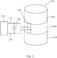
- Figure 3 is perspective view of the stack comprising the upper and lower dielectric sections 102c, d and the electrode structure 102e.
- the electrode structure 102e is in electrical connection with an RF power supply 130 through feed points 132, 134.
- a capacitor 136 is connected across the feed points 132, 134.
- the capacitor 136 tunes the electrode structure 102e to the drive frequency provided by the RF power supply 130.
- the frequency of the RF electrical signal provided by the RF power 130 may be 13.56MHz, 2MHz or any other convenient frequency. Frequency tuning may be employed to provide matching over a range of power and pressure conditions.
- the electrode structure 102e is in form of a non-continuous band which constitutes part of the chamber itself and also constitutes a single turn structure of an ICP plasma source for generating an inductively coupled plasma within the interior of the chamber 102.
- the skilled reader will appreciate that the single turn electrode structure 102e cannot extend completely around the periphery of the body portion of the chamber.
- a dielectric break 138 is provided which separates one circumferential end of the electrode structure from the other circumferential end.
- the dielectric break can be made of any convenient dielectric material. Typically the dielectric break is made of the same dielectric material that the upper and lower dielectric sections 102c, d are formed from.
- the electrode structure extends around the majority of the circumference of the chamber 102. For example, the electrode structure may extend around 320° or more of the periphery of the chamber and the dielectric break may extend around 40° or less of the periphery of the chamber.
- the apparatus described in Figures 2 and 3 utilises an ICP source which is fundamentally different from the prior art ICP sources of the type described above in relation to Figure 1 .
- the ICP source of the invention utilises the chamber wall itself as the primary winding of the ICP source. Therefore, the primary winding is immediately adjacent to the inductively coupled plasma itself within the chamber. This can lead to more efficient coupling and wider power/pressure operation regime. Operation at high power, high pressure, and/or high thermal loading is also possible.
- FIGs 4a and b show a second embodiment of the invention.
- Figure 4a shows a cylindrical electrode structure 140 which is another single turn structure that can be used as part of an ICP source.
- the single turn electrode structure 140 comprises a plurality of spaced apart band segments 140a, b, c, d. Adjacent band segments are separated by relatively thin dielectric breaks 142.
- the dielectric breaks can be formed from a dielectric material such as ceramic or quartz.
- Each band segment has apertures 144 formed therein allowing electrical connection to be made to the RF source. Additionally, each band segment comprises apertures 146 allowing connection to a cooling system which supplies a cooling fluid. The band segments further comprise internal passageways (not shown) which permit circulation for cooling fluid within the band segments.
- Figure 4b shows the band electrode structure 140 of Figure 4a interposed between an upper dielectric section 148 and a lower dielectric section 150. It will be appreciated that the three part cylindrical structure shown in Figure 4b is similar to the arrangement shown in Figure 3 . The structure shown in Figure 4b can be used as part of a chamber of the type shown in Figure 2 .
- RF feed lines 152 and tuning capacitors 154 which are connected across RF feed lines associated with adjacent band segments.
- Water cooling connections 156 are also shown in Figure 4b . The water cooling connections are in operative connection with the apertures 146 shown in Figure 4a .
- Figure 5 shows an electrical circuit which may be used to drive the band segments shown in Figure 4 with RF power from an RF power supply (not shown) via feed points 158, 159.
- the band segments 140a-d are connected in parallel with tuning capacitors 154 connected across adjacent band segments.
- the use of N sections connected in parallel reduces the applied voltage by a factor N. This can be advantageous in suppressing electric coupling around the dielectric breaks and feed points.
- the impedance may be less than 50 Ohms. In this instance, a step down from a typical generator may be required. In the four segment arrangement, the voltage applied is similar to that used in powering a single turn chamber wall. In these embodiments, the impedance may be reasonably close to 50 Ohms, allowing more efficient matching. High circulating currents only flow through the wall and the tuning capacitors.
- striking of the plasma can be assisted by using additional RF, AC or DC potentials briefly applied between the source and ground.
- additional RF, AC or DC potentials briefly applied between the source and ground is possible to power adjacent segments with alternate polarities of an additional power supply used for striking up a plasma.
- the band segments can have their midpoints grounded to minimize sputtering and other undesirable effects associated with the applied voltage. Selective grounding of the segments can also be used to assist in striking the plasma.
- Plasmas were produced using the apparatus shown in Figures 4 and 5 . Approximate dimensions of the electrode structure were ⁇ 70mm diameter, 30mm height with 6.35 mm thick aluminium band segment walls (ID ⁇ 57mm).
- the dielectric sections 148, 150 were formed from quartz with ⁇ 70mm OD and ⁇ 50mm height. Epoxy was used to bond the components together to provide a vacuum seal and isolation. Typical process conditions were ⁇ 3slpm N 2 , 10 Torr pressure using 1.3kW RF (at 13.65MHz). It will be appreciated that these conditions and configurations are merely representative and many other variations are possible.It is has been realised that, under many typical operating conditions, the plasma formed in the chamber is blown downstream (i.e., towards the substrate support and the pumping port).
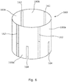
- FIG. 6 shows a further embodiment of an electrode structure, depicted generally at 160, which can reduce this unwanted thermal loading of the lower dielectric section.
- the electrode structure 160 comprises four band segments 160a-d which are separated by dielectric breaks 162.
- Each band segment has a discontinuity formed in a lower portion thereof, i.e., the region of each band segment which is closest to the pumping port.
- the discontinuities 164 can be a longer longitudinally extending slot, although other arrangements are possible.
- the discontinuities may be filled with a dielectric material although there may be instead no material disposed in the discontinuity.
- the discontinuities act to break up the path of primary current flow through the band segments. This results in primary current flow only circulating in the upper portions of the band segments. This can result in the plasma being confined to the upper regions of the band segments only so that, in use, the region of high thermal loading associated with the plasma remains inside the principally metallic electrode structure. This is advantageous because the metallic electrode structure is easy to cool, for example using a cooling fluid based system.
- the electrode structure may be connected to the upper and lower dielectric sections by any convenient means, such as through adhesives, flanges, o rings, or other means. In principle, it may be possible to provide a unitary structure formed using advanced deposition techniques.
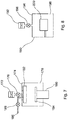
- FIG. 7 shows a third embodiment of a plasma processing apparatus of the invention, depicted generally at 170.
- the apparatus comprises a first chamber 172 and a second chamber 174.
- the first chamber 172 includes an electrode structure which is configured to act as a primary winding of inductively coupled plasma source in accordance with the principles set out above.
- the first chamber 172 acts as a plasma source for supplying radicals to the second chamber 174.
- the first chamber 172 is in communication with the second chamber 174 via an isolation valve 176.
- the second chamber 174 comprises a pumping port 178, a platen 180 and a shower head arrangement 182.
- the platen 180 supports a wafer 184.
- the shower head 182 introduces suitable process gases into the second chamber 174.
- the process gases are supplied through a gas supply system 186 which comprises an isolation valve 188.
- the apparatus 170 can function as a PE-CVD tool.
- the arrangement shown in Figure 7 is particularly useful for cleaning the second chamber 174. If the plasma was provided in the chamber 174 itself, either by electrically driving the shower head 182 or the platen 180, then ion-bombardment would occur which typically will wear down the chamber parts over a period of time.
- the first chamber 172 to supply radical species to the second chamber 174 with no significant concentrations of ions reaching the second chamber 174. In this way, a fast, low damage clean can be provided.
- the wafer 184 may not be present in the chamber during the cleaning process. In the case of silicon dioxide or silicon nitride cleans, fluorine radicals might be used, although the supply of other radicals is possible.
- FIG 8 shows a fourth embodiment of a plasma processing apparatus of the invention, depicted generally at 190.
- the apparatus 190 is another multiple chamber arrangement comprising a first chamber 192 and a second chamber 194. Similar to the arrangement shown in Figure 7 , the first chamber 192 comprises an electrode structure which is configured to act as a primary winding of an inductively coupled plasma source.
- the first chamber acts as a plasma source which supplies radicals to the second chamber 194 via an isolation valve 196.
- the second chamber 194 comprises a pumping port 198.
- a part 200 such as tool part, is suitably positioned in the second chamber 194.
- the radicals supplied by the first chamber 192 are used to modify the surface of the part 200 in a desired way.
- the part 200 may be a metal drill bit which is plasma processed to provide a nitride coating.
- the first chamber 192 can provide a source of radicals so that plasma processing can occur without any significant ion bombardment. Any suitable radical species, such as nitrogen or oxygen radicals, might be used.
- the apparatus 190 shown in Figure 8 might be used to provide other forms of radical based plasma processing where ion bombardment is unwanted.
- apparatus of this type can be used in epitaxial CVD. Ions (which tend to be quite directional) are unwanted because they can cause dislocations and defects in the growing crystal.
- a further advantage is that the temperature of the epitaxial cvd process can be reduced.
Landscapes
- Chemical & Material Sciences (AREA)
- Engineering & Computer Science (AREA)
- Physics & Mathematics (AREA)
- Plasma & Fusion (AREA)
- Analytical Chemistry (AREA)
- Mechanical Engineering (AREA)
- Materials Engineering (AREA)
- Metallurgy (AREA)
- Organic Chemistry (AREA)
- Chemical Kinetics & Catalysis (AREA)
- General Chemical & Material Sciences (AREA)
- Optics & Photonics (AREA)
- Chemical Vapour Deposition (AREA)
- Plasma Technology (AREA)
- Drying Of Semiconductors (AREA)
Applications Claiming Priority (1)
| Application Number | Priority Date | Filing Date | Title |
|---|---|---|---|
| GBGB1603581.8A GB201603581D0 (en) | 2016-03-01 | 2016-03-01 | Plasma processing apparatus |
Publications (2)
| Publication Number | Publication Date |
|---|---|
| EP3214637A1 true EP3214637A1 (fr) | 2017-09-06 |
| EP3214637B1 EP3214637B1 (fr) | 2020-09-23 |
Family
ID=55807153
Family Applications (1)
| Application Number | Title | Priority Date | Filing Date |
|---|---|---|---|
| EP17158675.3A Active EP3214637B1 (fr) | 2016-03-01 | 2017-03-01 | Appareil et méthode de traitement de plasma |
Country Status (7)
| Country | Link |
|---|---|
| US (1) | US10446374B2 (fr) |
| EP (1) | EP3214637B1 (fr) |
| JP (1) | JP6807777B2 (fr) |
| KR (1) | KR102770695B1 (fr) |
| CN (1) | CN107146754B (fr) |
| GB (1) | GB201603581D0 (fr) |
| TW (1) | TWI784944B (fr) |
Cited By (2)
| Publication number | Priority date | Publication date | Assignee | Title |
|---|---|---|---|---|
| EP3611752A1 (fr) | 2018-08-17 | 2020-02-19 | SPTS Technologies Limited | Appareil au plasma |
| EP4064324A4 (fr) * | 2020-02-19 | 2023-12-06 | En2Core Technology, Inc | Structure d'antenne et dispositif de génération de plasma l'utilisant |
Families Citing this family (1)
| Publication number | Priority date | Publication date | Assignee | Title |
|---|---|---|---|---|
| GB201813467D0 (en) * | 2018-08-17 | 2018-10-03 | Spts Technologies Ltd | Method of depositing silicon nitride |
Citations (3)
| Publication number | Priority date | Publication date | Assignee | Title |
|---|---|---|---|---|
| EP0467046A2 (fr) * | 1990-07-17 | 1992-01-22 | Balzers Aktiengesellschaft | Installation de gravure ou de dépôt |
| US20040026231A1 (en) * | 2001-10-09 | 2004-02-12 | Pribyl Patrick A. | Plasma production device and method and RF driver circuit with adjustable duty cycle |
| EP2299789A1 (fr) * | 2008-05-22 | 2011-03-23 | EMD Corporation | Appareil de génération de plasma et appareil de traitement par plasma |
Family Cites Families (18)
| Publication number | Priority date | Publication date | Assignee | Title |
|---|---|---|---|---|
| DE4018070A1 (de) | 1990-06-06 | 1991-12-12 | Bayer Ag | Morpholinoharnstoff-derivate |
| US6077384A (en) | 1994-08-11 | 2000-06-20 | Applied Materials, Inc. | Plasma reactor having an inductive antenna coupling power through a parallel plate electrode |
| US5589737A (en) | 1994-12-06 | 1996-12-31 | Lam Research Corporation | Plasma processor for large workpieces |
| US5710486A (en) * | 1995-05-08 | 1998-01-20 | Applied Materials, Inc. | Inductively and multi-capacitively coupled plasma reactor |
| JPH09120957A (ja) * | 1995-08-23 | 1997-05-06 | Fujitsu Ltd | プラズマ装置及びプラズマ処理方法 |
| US6178920B1 (en) * | 1997-06-05 | 2001-01-30 | Applied Materials, Inc. | Plasma reactor with internal inductive antenna capable of generating helicon wave |
| DE10147998A1 (de) * | 2001-09-28 | 2003-04-10 | Unaxis Balzers Ag | Verfahren und Vorrichtung zur Erzeugung eines Plasmas |
| KR20050059858A (ko) * | 2003-12-15 | 2005-06-21 | 주성엔지니어링(주) | 다수의 전극블록으로 이루어지는 플라즈마 전극과 이를 이용하는 전원공급 시스템 |
| KR20050077165A (ko) * | 2004-01-27 | 2005-08-01 | 삼성전자주식회사 | 건식 식각 장치 |
| JP2010098174A (ja) * | 2008-10-17 | 2010-04-30 | Shibaura Mechatronics Corp | プラズマ処理装置 |
| KR101312695B1 (ko) | 2009-08-21 | 2013-09-27 | 맷슨 테크놀로지, 인크. | 유도 플라즈마 소스 |
| KR101711687B1 (ko) * | 2009-09-28 | 2017-03-02 | 램 리써치 코포레이션 | 일체형 한정 링 배열 및 그 방법 |
| JP2013191593A (ja) * | 2012-03-12 | 2013-09-26 | Tokyo Electron Ltd | プラズマ処理装置 |
| JP2013254723A (ja) * | 2012-05-11 | 2013-12-19 | Hitachi High-Technologies Corp | プラズマ処理装置 |
| US20140053984A1 (en) * | 2012-08-27 | 2014-02-27 | Hyun Ho Doh | Symmetric return liner for modulating azimuthal non-uniformity in a plasma processing system |
| JP6001963B2 (ja) | 2012-08-31 | 2016-10-05 | 東京エレクトロン株式会社 | プラズマ処理装置、プラズマ生成装置、アンテナ構造体及びプラズマ生成方法 |
| US20140141619A1 (en) * | 2012-11-19 | 2014-05-22 | Tokyo Electron Limited | Capacitively coupled plasma equipment with uniform plasma density |
| US9607819B1 (en) * | 2016-02-03 | 2017-03-28 | The Charles Stark Draper Laboratory Inc. | Non-radioactive, capacitive discharge plasma ion source and method |
-
2016
- 2016-03-01 GB GBGB1603581.8A patent/GB201603581D0/en not_active Ceased
-
2017
- 2017-02-28 KR KR1020170026297A patent/KR102770695B1/ko active Active
- 2017-03-01 TW TW106106625A patent/TWI784944B/zh active
- 2017-03-01 US US15/446,052 patent/US10446374B2/en active Active
- 2017-03-01 CN CN201710116676.0A patent/CN107146754B/zh active Active
- 2017-03-01 EP EP17158675.3A patent/EP3214637B1/fr active Active
- 2017-03-01 JP JP2017038127A patent/JP6807777B2/ja active Active
Patent Citations (3)
| Publication number | Priority date | Publication date | Assignee | Title |
|---|---|---|---|---|
| EP0467046A2 (fr) * | 1990-07-17 | 1992-01-22 | Balzers Aktiengesellschaft | Installation de gravure ou de dépôt |
| US20040026231A1 (en) * | 2001-10-09 | 2004-02-12 | Pribyl Patrick A. | Plasma production device and method and RF driver circuit with adjustable duty cycle |
| EP2299789A1 (fr) * | 2008-05-22 | 2011-03-23 | EMD Corporation | Appareil de génération de plasma et appareil de traitement par plasma |
Cited By (4)
| Publication number | Priority date | Publication date | Assignee | Title |
|---|---|---|---|---|
| EP3611752A1 (fr) | 2018-08-17 | 2020-02-19 | SPTS Technologies Limited | Appareil au plasma |
| US10720308B2 (en) | 2018-08-17 | 2020-07-21 | Spts Technologies Limited | Plasma apparatus |
| EP4064324A4 (fr) * | 2020-02-19 | 2023-12-06 | En2Core Technology, Inc | Structure d'antenne et dispositif de génération de plasma l'utilisant |
| US12205794B2 (en) | 2020-02-19 | 2025-01-21 | En2core Technology Inc. | Antenna structure and plasma generating device using same |
Also Published As
| Publication number | Publication date |
|---|---|
| GB201603581D0 (en) | 2016-04-13 |
| KR102770695B1 (ko) | 2025-02-19 |
| EP3214637B1 (fr) | 2020-09-23 |
| CN107146754A (zh) | 2017-09-08 |
| CN107146754B (zh) | 2020-08-07 |
| US10446374B2 (en) | 2019-10-15 |
| JP6807777B2 (ja) | 2021-01-06 |
| TWI784944B (zh) | 2022-12-01 |
| KR20170102438A (ko) | 2017-09-11 |
| US20170256384A1 (en) | 2017-09-07 |
| JP2017157560A (ja) | 2017-09-07 |
| TW201742678A (zh) | 2017-12-16 |
Similar Documents
| Publication | Publication Date | Title |
|---|---|---|
| US9767996B2 (en) | Application of powered electrostatic faraday shield to recondition dielectric window in ICP plasmas | |
| US20210217591A1 (en) | Process chamber for cyclic and selective material removal and etching | |
| US7105102B2 (en) | Vacuum plasma processor having a chamber with electrodes and a coil for plasma excitation and method of operating same | |
| KR101094124B1 (ko) | 균일한 프로세스 레이트를 발생시키는 안테나 | |
| KR101546278B1 (ko) | 플라스마 챔버의 조정가능한 접지 평면 | |
| US6727654B2 (en) | Plasma processing apparatus | |
| CN1314072C (zh) | 抑制电弧放电的对应等离子体喷头rf顶电极调谐的merie等离子体反应器 | |
| US7767056B2 (en) | High-frequency plasma processing apparatus | |
| US7632375B2 (en) | Electrically enhancing the confinement of plasma | |
| CN114975064A (zh) | 混合等离子体源阵列 | |
| EP3214637B1 (fr) | Appareil et méthode de traitement de plasma | |
| EP3611752B1 (fr) | Appareil au plasma | |
| US20090151636A1 (en) | Rpsc and rf feedthrough | |
| KR20220017961A (ko) | 정전 척을 구비하는 기판 처리 시스템 | |
| US7323081B2 (en) | High-frequency plasma processing apparatus | |
| US6824363B2 (en) | Linear inductive plasma pump for process reactors | |
| US20240412957A1 (en) | High temperature biasable heater with advanced far edge electrode, electrostatic chuck, and embedded ground electrode | |
| KR20180072916A (ko) | 기판 처리 장치 | |
| US20250316520A1 (en) | Bipolar esc to prevent substrate backside discharging | |
| US20250391700A1 (en) | Hybrid vacuum electrostatic chuck | |
| JPH08335569A (ja) | プラズマ処理装置 |
Legal Events
| Date | Code | Title | Description |
|---|---|---|---|
| PUAI | Public reference made under article 153(3) epc to a published international application that has entered the european phase |
Free format text: ORIGINAL CODE: 0009012 |
|
| STAA | Information on the status of an ep patent application or granted ep patent |
Free format text: STATUS: THE APPLICATION HAS BEEN PUBLISHED |
|
| AK | Designated contracting states |
Kind code of ref document: A1 Designated state(s): AL AT BE BG CH CY CZ DE DK EE ES FI FR GB GR HR HU IE IS IT LI LT LU LV MC MK MT NL NO PL PT RO RS SE SI SK SM TR |
|
| AX | Request for extension of the european patent |
Extension state: BA ME |
|
| STAA | Information on the status of an ep patent application or granted ep patent |
Free format text: STATUS: REQUEST FOR EXAMINATION WAS MADE |
|
| 17P | Request for examination filed |
Effective date: 20180306 |
|
| RBV | Designated contracting states (corrected) |
Designated state(s): AL AT BE BG CH CY CZ DE DK EE ES FI FR GB GR HR HU IE IS IT LI LT LU LV MC MK MT NL NO PL PT RO RS SE SI SK SM TR |
|
| STAA | Information on the status of an ep patent application or granted ep patent |
Free format text: STATUS: EXAMINATION IS IN PROGRESS |
|
| 17Q | First examination report despatched |
Effective date: 20190725 |
|
| GRAP | Despatch of communication of intention to grant a patent |
Free format text: ORIGINAL CODE: EPIDOSNIGR1 |
|
| STAA | Information on the status of an ep patent application or granted ep patent |
Free format text: STATUS: GRANT OF PATENT IS INTENDED |
|
| INTG | Intention to grant announced |
Effective date: 20200421 |
|
| GRAS | Grant fee paid |
Free format text: ORIGINAL CODE: EPIDOSNIGR3 |
|
| GRAA | (expected) grant |
Free format text: ORIGINAL CODE: 0009210 |
|
| STAA | Information on the status of an ep patent application or granted ep patent |
Free format text: STATUS: THE PATENT HAS BEEN GRANTED |
|
| AK | Designated contracting states |
Kind code of ref document: B1 Designated state(s): AL AT BE BG CH CY CZ DE DK EE ES FI FR GB GR HR HU IE IS IT LI LT LU LV MC MK MT NL NO PL PT RO RS SE SI SK SM TR |
|
| REG | Reference to a national code |
Ref country code: GB Ref legal event code: FG4D |
|
| REG | Reference to a national code |
Ref country code: CH Ref legal event code: EP |
|
| REG | Reference to a national code |
Ref country code: DE Ref legal event code: R082 Ref document number: 602017023959 Country of ref document: DE Representative=s name: ZEITLER VOLPERT KANDLBINDER PATENT- UND RECHTS, DE Ref country code: DE Ref legal event code: R082 Ref document number: 602017023959 Country of ref document: DE Representative=s name: ZEITLER VOLPERT KANDLBINDER PATENTANWAELTE PAR, DE |
|
| REG | Reference to a national code |
Ref country code: DE Ref legal event code: R096 Ref document number: 602017023959 Country of ref document: DE |
|
| REG | Reference to a national code |
Ref country code: IE Ref legal event code: FG4D |
|
| REG | Reference to a national code |
Ref country code: AT Ref legal event code: REF Ref document number: 1317229 Country of ref document: AT Kind code of ref document: T Effective date: 20201015 |
|
| PG25 | Lapsed in a contracting state [announced via postgrant information from national office to epo] |
Ref country code: BG Free format text: LAPSE BECAUSE OF FAILURE TO SUBMIT A TRANSLATION OF THE DESCRIPTION OR TO PAY THE FEE WITHIN THE PRESCRIBED TIME-LIMIT Effective date: 20201223 Ref country code: SE Free format text: LAPSE BECAUSE OF FAILURE TO SUBMIT A TRANSLATION OF THE DESCRIPTION OR TO PAY THE FEE WITHIN THE PRESCRIBED TIME-LIMIT Effective date: 20200923 Ref country code: GR Free format text: LAPSE BECAUSE OF FAILURE TO SUBMIT A TRANSLATION OF THE DESCRIPTION OR TO PAY THE FEE WITHIN THE PRESCRIBED TIME-LIMIT Effective date: 20201224 Ref country code: HR Free format text: LAPSE BECAUSE OF FAILURE TO SUBMIT A TRANSLATION OF THE DESCRIPTION OR TO PAY THE FEE WITHIN THE PRESCRIBED TIME-LIMIT Effective date: 20200923 Ref country code: FI Free format text: LAPSE BECAUSE OF FAILURE TO SUBMIT A TRANSLATION OF THE DESCRIPTION OR TO PAY THE FEE WITHIN THE PRESCRIBED TIME-LIMIT Effective date: 20200923 Ref country code: NO Free format text: LAPSE BECAUSE OF FAILURE TO SUBMIT A TRANSLATION OF THE DESCRIPTION OR TO PAY THE FEE WITHIN THE PRESCRIBED TIME-LIMIT Effective date: 20201223 |
|
| REG | Reference to a national code |
Ref country code: AT Ref legal event code: MK05 Ref document number: 1317229 Country of ref document: AT Kind code of ref document: T Effective date: 20200923 |
|
| PG25 | Lapsed in a contracting state [announced via postgrant information from national office to epo] |
Ref country code: RS Free format text: LAPSE BECAUSE OF FAILURE TO SUBMIT A TRANSLATION OF THE DESCRIPTION OR TO PAY THE FEE WITHIN THE PRESCRIBED TIME-LIMIT Effective date: 20200923 Ref country code: LV Free format text: LAPSE BECAUSE OF FAILURE TO SUBMIT A TRANSLATION OF THE DESCRIPTION OR TO PAY THE FEE WITHIN THE PRESCRIBED TIME-LIMIT Effective date: 20200923 |
|
| REG | Reference to a national code |
Ref country code: NL Ref legal event code: MP Effective date: 20200923 |
|
| REG | Reference to a national code |
Ref country code: LT Ref legal event code: MG4D |
|
| PG25 | Lapsed in a contracting state [announced via postgrant information from national office to epo] |
Ref country code: SM Free format text: LAPSE BECAUSE OF FAILURE TO SUBMIT A TRANSLATION OF THE DESCRIPTION OR TO PAY THE FEE WITHIN THE PRESCRIBED TIME-LIMIT Effective date: 20200923 Ref country code: EE Free format text: LAPSE BECAUSE OF FAILURE TO SUBMIT A TRANSLATION OF THE DESCRIPTION OR TO PAY THE FEE WITHIN THE PRESCRIBED TIME-LIMIT Effective date: 20200923 Ref country code: LT Free format text: LAPSE BECAUSE OF FAILURE TO SUBMIT A TRANSLATION OF THE DESCRIPTION OR TO PAY THE FEE WITHIN THE PRESCRIBED TIME-LIMIT Effective date: 20200923 Ref country code: CZ Free format text: LAPSE BECAUSE OF FAILURE TO SUBMIT A TRANSLATION OF THE DESCRIPTION OR TO PAY THE FEE WITHIN THE PRESCRIBED TIME-LIMIT Effective date: 20200923 Ref country code: RO Free format text: LAPSE BECAUSE OF FAILURE TO SUBMIT A TRANSLATION OF THE DESCRIPTION OR TO PAY THE FEE WITHIN THE PRESCRIBED TIME-LIMIT Effective date: 20200923 Ref country code: PT Free format text: LAPSE BECAUSE OF FAILURE TO SUBMIT A TRANSLATION OF THE DESCRIPTION OR TO PAY THE FEE WITHIN THE PRESCRIBED TIME-LIMIT Effective date: 20210125 |
|
| PG25 | Lapsed in a contracting state [announced via postgrant information from national office to epo] |
Ref country code: PL Free format text: LAPSE BECAUSE OF FAILURE TO SUBMIT A TRANSLATION OF THE DESCRIPTION OR TO PAY THE FEE WITHIN THE PRESCRIBED TIME-LIMIT Effective date: 20200923 Ref country code: IS Free format text: LAPSE BECAUSE OF FAILURE TO SUBMIT A TRANSLATION OF THE DESCRIPTION OR TO PAY THE FEE WITHIN THE PRESCRIBED TIME-LIMIT Effective date: 20210123 Ref country code: ES Free format text: LAPSE BECAUSE OF FAILURE TO SUBMIT A TRANSLATION OF THE DESCRIPTION OR TO PAY THE FEE WITHIN THE PRESCRIBED TIME-LIMIT Effective date: 20200923 Ref country code: AT Free format text: LAPSE BECAUSE OF FAILURE TO SUBMIT A TRANSLATION OF THE DESCRIPTION OR TO PAY THE FEE WITHIN THE PRESCRIBED TIME-LIMIT Effective date: 20200923 Ref country code: AL Free format text: LAPSE BECAUSE OF FAILURE TO SUBMIT A TRANSLATION OF THE DESCRIPTION OR TO PAY THE FEE WITHIN THE PRESCRIBED TIME-LIMIT Effective date: 20200923 |
|
| REG | Reference to a national code |
Ref country code: DE Ref legal event code: R097 Ref document number: 602017023959 Country of ref document: DE |
|
| PG25 | Lapsed in a contracting state [announced via postgrant information from national office to epo] |
Ref country code: SK Free format text: LAPSE BECAUSE OF FAILURE TO SUBMIT A TRANSLATION OF THE DESCRIPTION OR TO PAY THE FEE WITHIN THE PRESCRIBED TIME-LIMIT Effective date: 20200923 |
|
| PLBE | No opposition filed within time limit |
Free format text: ORIGINAL CODE: 0009261 |
|
| STAA | Information on the status of an ep patent application or granted ep patent |
Free format text: STATUS: NO OPPOSITION FILED WITHIN TIME LIMIT |
|
| PG25 | Lapsed in a contracting state [announced via postgrant information from national office to epo] |
Ref country code: SI Free format text: LAPSE BECAUSE OF FAILURE TO SUBMIT A TRANSLATION OF THE DESCRIPTION OR TO PAY THE FEE WITHIN THE PRESCRIBED TIME-LIMIT Effective date: 20200923 Ref country code: DK Free format text: LAPSE BECAUSE OF FAILURE TO SUBMIT A TRANSLATION OF THE DESCRIPTION OR TO PAY THE FEE WITHIN THE PRESCRIBED TIME-LIMIT Effective date: 20200923 |
|
| 26N | No opposition filed |
Effective date: 20210624 |
|
| PG25 | Lapsed in a contracting state [announced via postgrant information from national office to epo] |
Ref country code: IT Free format text: LAPSE BECAUSE OF FAILURE TO SUBMIT A TRANSLATION OF THE DESCRIPTION OR TO PAY THE FEE WITHIN THE PRESCRIBED TIME-LIMIT Effective date: 20200923 Ref country code: MC Free format text: LAPSE BECAUSE OF FAILURE TO SUBMIT A TRANSLATION OF THE DESCRIPTION OR TO PAY THE FEE WITHIN THE PRESCRIBED TIME-LIMIT Effective date: 20200923 |
|
| REG | Reference to a national code |
Ref country code: CH Ref legal event code: PL |
|
| GBPC | Gb: european patent ceased through non-payment of renewal fee |
Effective date: 20210301 |
|
| REG | Reference to a national code |
Ref country code: BE Ref legal event code: MM Effective date: 20210331 |
|
| PG25 | Lapsed in a contracting state [announced via postgrant information from national office to epo] |
Ref country code: IE Free format text: LAPSE BECAUSE OF NON-PAYMENT OF DUE FEES Effective date: 20210301 Ref country code: LU Free format text: LAPSE BECAUSE OF NON-PAYMENT OF DUE FEES Effective date: 20210301 Ref country code: LI Free format text: LAPSE BECAUSE OF NON-PAYMENT OF DUE FEES Effective date: 20210331 Ref country code: CH Free format text: LAPSE BECAUSE OF NON-PAYMENT OF DUE FEES Effective date: 20210331 Ref country code: GB Free format text: LAPSE BECAUSE OF NON-PAYMENT OF DUE FEES Effective date: 20210301 |
|
| PG25 | Lapsed in a contracting state [announced via postgrant information from national office to epo] |
Ref country code: BE Free format text: LAPSE BECAUSE OF NON-PAYMENT OF DUE FEES Effective date: 20210331 |
|
| REG | Reference to a national code |
Ref country code: FR Ref legal event code: PLFP Year of fee payment: 7 |
|
| PG25 | Lapsed in a contracting state [announced via postgrant information from national office to epo] |
Ref country code: HU Free format text: LAPSE BECAUSE OF FAILURE TO SUBMIT A TRANSLATION OF THE DESCRIPTION OR TO PAY THE FEE WITHIN THE PRESCRIBED TIME-LIMIT; INVALID AB INITIO Effective date: 20170301 |
|
| PG25 | Lapsed in a contracting state [announced via postgrant information from national office to epo] |
Ref country code: NL Free format text: LAPSE BECAUSE OF NON-PAYMENT OF DUE FEES Effective date: 20200923 Ref country code: CY Free format text: LAPSE BECAUSE OF FAILURE TO SUBMIT A TRANSLATION OF THE DESCRIPTION OR TO PAY THE FEE WITHIN THE PRESCRIBED TIME-LIMIT Effective date: 20200923 |
|
| P01 | Opt-out of the competence of the unified patent court (upc) registered |
Effective date: 20230525 |
|
| REG | Reference to a national code |
Ref country code: DE Ref legal event code: R082 Ref document number: 602017023959 Country of ref document: DE Representative=s name: KANDLBINDER, MARKUS, DIPL.-PHYS., DE |
|
| PG25 | Lapsed in a contracting state [announced via postgrant information from national office to epo] |
Ref country code: MK Free format text: LAPSE BECAUSE OF FAILURE TO SUBMIT A TRANSLATION OF THE DESCRIPTION OR TO PAY THE FEE WITHIN THE PRESCRIBED TIME-LIMIT Effective date: 20200923 |
|
| PG25 | Lapsed in a contracting state [announced via postgrant information from national office to epo] |
Ref country code: MT Free format text: LAPSE BECAUSE OF FAILURE TO SUBMIT A TRANSLATION OF THE DESCRIPTION OR TO PAY THE FEE WITHIN THE PRESCRIBED TIME-LIMIT Effective date: 20200923 |
|
| PG25 | Lapsed in a contracting state [announced via postgrant information from national office to epo] |
Ref country code: TR Free format text: LAPSE BECAUSE OF FAILURE TO SUBMIT A TRANSLATION OF THE DESCRIPTION OR TO PAY THE FEE WITHIN THE PRESCRIBED TIME-LIMIT Effective date: 20200923 |
|
| PGFP | Annual fee paid to national office [announced via postgrant information from national office to epo] |
Ref country code: DE Payment date: 20260327 Year of fee payment: 10 |
|
| PGFP | Annual fee paid to national office [announced via postgrant information from national office to epo] |
Ref country code: FR Payment date: 20260325 Year of fee payment: 10 |