EP3217649A1 - Bilderfassungssensor mit erweiterter zeitverzögerung und integration - Google Patents
Bilderfassungssensor mit erweiterter zeitverzögerung und integration Download PDFInfo
- Publication number
- EP3217649A1 EP3217649A1 EP17158608.4A EP17158608A EP3217649A1 EP 3217649 A1 EP3217649 A1 EP 3217649A1 EP 17158608 A EP17158608 A EP 17158608A EP 3217649 A1 EP3217649 A1 EP 3217649A1
- Authority
- EP
- European Patent Office
- Prior art keywords
- image
- image data
- matrices
- vectors
- image sensor
- Prior art date
- Legal status (The legal status is an assumption and is not a legal conclusion. Google has not performed a legal analysis and makes no representation as to the accuracy of the status listed.)
- Granted
Links
Images

Classifications
-
- H—ELECTRICITY
- H04—ELECTRIC COMMUNICATION TECHNIQUE
- H04N—PICTORIAL COMMUNICATION, e.g. TELEVISION
- H04N25/00—Circuitry of solid-state image sensors [SSIS]; Control thereof
- H04N25/70—SSIS architectures; Circuits associated therewith
- H04N25/76—Addressed sensors, e.g. MOS or CMOS sensors
- H04N25/768—Addressed sensors, e.g. MOS or CMOS sensors for time delay and integration [TDI]
Definitions
- the invention relates to an image sensor of the type called "Time Delay and Integration” (TDI).
- TDI Time Delay and Integration
- Such a sensor is adapted to be embedded in a carrier (satellite or aircraft) moving over a scene to be observed; it is particularly suitable for space applications.
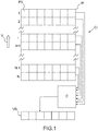
- the principle of a TDI image sensor is illustrated on the figure 1 .
- the IC sensor comprises an array M of pixels PX, arranged in rows (or rows) and columns; in the figure, the lines are numbered from 1 to N.
- the carrier in which it is embarked moves with a speed V in the direction D, perpendicular to the lines; therefore the image of the observed scene, formed on the matrix by an optical system not shown, scrolls in the same direction, with the opposite orientation to V.
- the interval ⁇ t depends both on the desired spatial resolution (function of the magnification of the optical system and the size of the pixels) and on the speed of displacement V of the carrier relative to the ground.
- An electronic circuit C integrates the signals generated by the different rows of pixels of the matrix and corresponding to the same line of the image.
- the circuit C provides a vector of image data VD representative of said line of the optical image, integrated over a time equal to N ⁇ ⁇ t, which makes it possible to increase the signal-to-noise ratio of the data of image acquired by the sensor.
- the document FR 2 967 754 teaches a technique to partially overcome this limitation.
- This document discloses a sensor comprising a plurality of TDI-type image detection arrays, aligned in the running direction of the image, and an optical motion sensor (or “motion detector”) consisting of elongated pixels oriented in two mutually orthogonal directions.
- Each of the individual detection matrices 1 carries out a TDI integration on N lines, the number N being small enough that the accumulation of imperfections remains tolerable.
- m image data vectors are thus obtained ("image data” is understood to mean a numerical value representing the luminous intensity associated with a pixel) each corresponding to a integration on N lines.
- the optical movement sensor makes it possible to associate a "shake" (shift) with each of these vectors; an electronic processing circuit corrects this shake and sum vectors associated with the same line of the optical image.
- the aim of the invention is to overcome these drawbacks of the prior art, and more particularly to provide a TDI-type image sensor which makes it possible to integrate a large number of lines while being able to be easily produced from standard components. .
- this object is achieved by detecting the shake performed directly from the image data acquired by a plurality of TDI detection arrays aligned in the running direction of the optical image, by a calculation of cross correlation.
- This "intrinsic" detection avoids the need to provide ad hoc sensors, unconventional and requiring extremely accurate alignment.
- the intrinsic nature of motion detection also makes it sensitive to the effects of optical distortion and misalignment.
- a programmable digital circuit such as an FPGA (acronym for "Field Programmable Gate Array ", that is, programmable gate array in situ ).
- Another object of the invention is an optical spatial or airborne image acquisition instrument comprising such an image sensor.
- the Figure 2A illustrates a CIM image sensor according to a first embodiment of the invention.
- This sensor comprises two detection matrices CTI, identified by the references M1 and M2, and a signal processing circuit CTS having two input ports connected to respective output ports of said detection matrices.
- Each of the detection matrices, M1, M2, constituted by a respective monolithic integrated circuit IC1, IC2, comprises a sensitive part, formed by lines L 1 1 -L 1 N , L 2 1 -L 2 N of M parallel light-sensitive pixels. between them and with the lines of the other matrix, and a processing circuit C1, C2 whose operation has been described above with reference to the figure 1 .
- the matrices M1, M2 can for example be performed in CCD technology (Charge-Coupled Device) or CMOS.
- the two matrices are aligned in a direction D, perpendicular to the orientation of the lines and coinciding with the direction of movement of a carrier in which the sensor is embarked; the arrow V indicates the direction of this movement.
- an optical image formed by an onboard optical system scrolls on the sensor in the direction D, with a direction opposite to that of the movement of the carrier.
- a line of the optical image first illuminates the pixel line L 1 N of the matrix M1, then its line L 1 N-1 and so on until the line L 1 1 , then the spacing E between the active regions of the two matrices, then the line L 2 1 of the matrix M2, then its line L 2 2 and so on until the line L 2 N.
- the two detection matrices are arranged "head-to-tail", with their active portions opposite, so as to minimize the width of the spacing E.
- the optical image scrolls on the matrix M1 in a direction opposite to that of the numbering of its lines; the processing circuit C1 of this matrix must therefore operate "in reverse mode", integrating the signals of the different lines in the inverse order, while the processing circuit C2 of the matrix M2 operates "in forward mode", as the circuit C of the figure 1 .
- This ability to integrate in either front or back mode is native to commercial CMOS sensors.
- the processing circuit C1 of the matrix M1 produces at its output a series of data vectors VD1 representative of respective lines of the optical image, integrated over a time equal to N ⁇ ⁇ t, where N is the number of rows of the matrix and ⁇ t is the time of integration of the image on each line.
- the processing circuit C1 of the matrix M2 produces at its output a series of data vectors VD2 representative of respective lines of the optical image, integrated over a time equal to N ⁇ ⁇ t.
- a data vector is generated at each integration step ⁇ t.
- the data vectors VD1, VD2 are in the form of digital electronic signals, the analog-digital conversion being performed inside the arrays, and in particular of their processing circuits C1, C2.
- the vectors VD1, VD2 could have an analog nature, a conversion in digital format then being performed by the CTS signal processing circuit.
- the signal processing circuit CTS receives at its inputs the vectors VD1 and VD2, and uses it to calculate a vector of VDI image data (generally in the form of a digital electronic signal) corresponding to a time of doubled integration, that is equal to 2 ⁇ N ⁇ ⁇ t. To do this, however, it must first detect the offset between VD1 and VD2 caused, then correct them by recalibrating the vectors, and finally add them to obtain the VDI accumulated image data vector.
- the offset between the vectors VD1, VD2 is caused by the fluctuations of the pointing direction during the integration time, but also by possible alignment errors of the two matrices between them and / or with the direction D, or even by optical distortions. Unlike the case of the document FR 2 967 754 this shift is not detected by dedicated motion sensors, but directly from the VD1, VD2 vectors themselves; we can speak of intrinsic shake detection. As discussed above, this approach has a number of advantages: first, it avoids the use of additional and non-standard sensors that would impact the cost of the CIM image sensor; secondly, it allows the detection of offsets due to imperfect alignment of the detection matrices and to optical distortions. In turn, this makes it possible to relax the manufacturing constraints, and more particularly to use detection matrices made in the form of separate integrated circuits.
- the intrinsic detection of the shake is performed by calculating a cross correlation between the image data vectors VD1 and VD2.
- the cross-correlation between two data vectors of M elements numbered from 1 to M is a vector containing (2M-1) elements numbered from - (M-1) to + (M-1).
- the offset between the vectors VD1 and VD2 is given by the index of the element of this vector corresponding to the maximum of the cross-correlation (M being large, while the offsets are generally quite small, it may be appropriate to calculate correlation only for a limited number of offsets around zero). In this way, there is an offset that necessarily corresponds to an integer number of pixels.
- a radiometric correction of the vectors VD1, VD2 is performed before proceeding with the detection and correction of the shake in order to correct the dispersion of the gains and the dark currents of the TDI sensors M1 and M2.
- the signal processing circuit CTS is preferably made from a programmable logic component such as an FPGA, but it can also be a timely programmed processor. It is preferably embedded on the same carrier as the detection matrices; it would also be possible to transmit the VD1, VD2 vectors to the ground and perform the treatments, but this solution is less advantageous because it induces an increase in the flow of data to be transmitted.
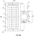
- each buffer function as shift registers: at each integration step, the oldest data vector is cleared, the other data vectors move one unit of memory, and a new data vector is stored.
- the contents of each buffer represent a matrix whose lines are the image data vectors.
- a two-dimensional cross-correlation (2DXC block in the CTS signal processing circuit of the Figure 2B ) makes it possible to find the offset, and thus the two-dimensional shake, between two matrices of image data acquired by separate sensors.
- the matrices are then recalibrated and integrated, as is done for the vectors in the first embodiment.
- the result is an accumulated image data matrix whose lines are VDI vectors.
- each buffer can store only a small number of data vectors images (typically three or four, usually no more than 10), which keeps the complexity of the calculations at an acceptable level.
- the buffers can be integrated in the CTS signal processing circuit, as in the case illustrated in FIG. Figure 2B but this is not essential; they may also be separate components. In principle, the buffers can even be integrated in the processing circuits C1, C2 associated with the detection matrices, but this then requires the use of non-standard components.
- the figure 3 very schematically illustrates a SAT carrier (for example a spacecraft, and more particularly a satellite) equipped with an optical image acquisition instrument comprising a conventional optical system SO, for example a telescope, coupled to an image sensor CIM according to one embodiment of the invention.
- a SAT carrier for example a spacecraft, and more particularly a satellite
- an optical image acquisition instrument comprising a conventional optical system SO, for example a telescope, coupled to an image sensor CIM according to one embodiment of the invention.
- each matrix will generally have a number of columns (M) different from the number of lines (N).
- the number of rows and columns may not be the same from one matrix to another. Even in the case where the number of matrices is equal to two, the back-to-back arrangement is not essential: it is only advantageous in order to reduce the gap E between the active parts of the matrices, and therefore the amplitude of the offset to correct; preferably this spacing should not exceed 3,000 or even 5,000 times the size of a pixel.
Landscapes
- Engineering & Computer Science (AREA)
- Multimedia (AREA)
- Signal Processing (AREA)
- Image Processing (AREA)
Applications Claiming Priority (1)
| Application Number | Priority Date | Filing Date | Title |
|---|---|---|---|
| FR1600405A FR3048842B1 (fr) | 2016-03-11 | 2016-03-11 | Capteur d'images par decalage temporel et integration etendue |
Publications (2)
| Publication Number | Publication Date |
|---|---|
| EP3217649A1 true EP3217649A1 (de) | 2017-09-13 |
| EP3217649B1 EP3217649B1 (de) | 2019-02-27 |
Family
ID=56555425
Family Applications (1)
| Application Number | Title | Priority Date | Filing Date |
|---|---|---|---|
| EP17158608.4A Active EP3217649B1 (de) | 2016-03-11 | 2017-03-01 | Bilderfassungssensor mit erweiterter zeitverzögerung und integration |
Country Status (3)
| Country | Link |
|---|---|
| EP (1) | EP3217649B1 (de) |
| ES (1) | ES2726732T3 (de) |
| FR (1) | FR3048842B1 (de) |
Cited By (1)
| Publication number | Priority date | Publication date | Assignee | Title |
|---|---|---|---|---|
| WO2023213598A1 (fr) | 2022-05-03 | 2023-11-09 | Airbus Defence And Space Sas | Procédé de génération d'image par un satellite par fusion à bord d'images acquises par ledit satellite |
Citations (4)
| Publication number | Priority date | Publication date | Assignee | Title |
|---|---|---|---|---|
| FR2893140A1 (fr) * | 2005-11-04 | 2007-05-11 | Atmel Grenoble Soc Par Actions | Capteur de vitesse au sol d'un vehicule |
| US20120127331A1 (en) * | 2010-11-22 | 2012-05-24 | Thomas J Grycewicz | Imaging Geometries for Scanning Optical Detectors with Overlapping Fields of Regard and Methods for Providing and Utilizing Same |
| FR2967754A1 (fr) | 2010-11-19 | 2012-05-25 | Gen Electric | Premelangeur pour chambre de combustion |
| FR2976754A1 (fr) * | 2011-06-15 | 2012-12-21 | Centre Nat Etd Spatiales | Capteur d'images avec correction de bouge par recalage numerique de prises de vue fractionnees |
-
2016
- 2016-03-11 FR FR1600405A patent/FR3048842B1/fr not_active Expired - Fee Related
-
2017
- 2017-03-01 ES ES17158608T patent/ES2726732T3/es active Active
- 2017-03-01 EP EP17158608.4A patent/EP3217649B1/de active Active
Patent Citations (4)
| Publication number | Priority date | Publication date | Assignee | Title |
|---|---|---|---|---|
| FR2893140A1 (fr) * | 2005-11-04 | 2007-05-11 | Atmel Grenoble Soc Par Actions | Capteur de vitesse au sol d'un vehicule |
| FR2967754A1 (fr) | 2010-11-19 | 2012-05-25 | Gen Electric | Premelangeur pour chambre de combustion |
| US20120127331A1 (en) * | 2010-11-22 | 2012-05-24 | Thomas J Grycewicz | Imaging Geometries for Scanning Optical Detectors with Overlapping Fields of Regard and Methods for Providing and Utilizing Same |
| FR2976754A1 (fr) * | 2011-06-15 | 2012-12-21 | Centre Nat Etd Spatiales | Capteur d'images avec correction de bouge par recalage numerique de prises de vue fractionnees |
Cited By (2)
| Publication number | Priority date | Publication date | Assignee | Title |
|---|---|---|---|---|
| WO2023213598A1 (fr) | 2022-05-03 | 2023-11-09 | Airbus Defence And Space Sas | Procédé de génération d'image par un satellite par fusion à bord d'images acquises par ledit satellite |
| FR3135329A1 (fr) * | 2022-05-03 | 2023-11-10 | Airbus Defence And Space Sas | Procédé de génération d’image par un satellite par fusion à bord d’images acquises par ledit satellite |
Also Published As
| Publication number | Publication date |
|---|---|
| EP3217649B1 (de) | 2019-02-27 |
| FR3048842B1 (fr) | 2018-03-02 |
| ES2726732T3 (es) | 2019-10-08 |
| FR3048842A1 (fr) | 2017-09-15 |
Similar Documents
| Publication | Publication Date | Title |
|---|---|---|
| EP2056590B1 (de) | Verfahren und Vorrichtung zum Pixelsauslesen aus einer bidimensionalen Matrix | |
| FR2961021A1 (fr) | Capteur d'image linéaire en technologie cmos a compensation d'effet de file | |
| EP3376544A1 (de) | Optische bildanzeigevorrichtung | |
| EP2735901B1 (de) | Bildgebungsgerät mit mehreren Erkennungseinheiten, die auf einer Brennebene angeordnet sind | |
| EP3122035B1 (de) | Bildsensor mit aktiven pixeln mit global-shutter-betriebsmodus, substraktion des reset-geräusches und nicht-destruktiver bildwiedergabe | |
| FR2991785A1 (fr) | Stabilisation d'une ligne de visee d'un systeme d'imagerie embarque a bord d'un satellite | |
| EP0738074A1 (de) | Detektionsverfahren mit verteilten Integrations- und Ausleseperioden für eine Abtastungskamera, und entsprechende Detektoranordnung | |
| EP3217649B1 (de) | Bilderfassungssensor mit erweiterter zeitverzögerung und integration | |
| EP3777129B1 (de) | Luftbildsensor zur aufnahme von matrixbildern durch zeitliche verschiebung und multispektrale summation | |
| EP3301644B1 (de) | Verfahren zur erstellung einer tiefenkarte einer szene und/oder eines vollkommen fokussierten bildes | |
| WO2014195622A1 (fr) | Capteur CMOS à photosites standard | |
| EP3402178B1 (de) | Bewegungssensor und bildsensor | |
| EP3839814B1 (de) | Bordseitiges optisches beobachtungsinstrument mit variabler räumlicher und spektraler auflösung | |
| FR3041458A1 (fr) | Dispositif d'imagerie, vehicule automobile equipe d'un tel dispositif d'imagerie, et procede associe | |
| EP4186227B1 (de) | Flugzeitsensor für abstandsmessung mit pixel mit mehreren speicherknoten | |
| EP4405648A1 (de) | Verfahren zur erfassung multispektraler bilder und panchromatischer miniaturbilder | |
| EP4203490A1 (de) | Beobachtungssystem und beobachtungsverfahren | |
| EP3165875B1 (de) | Verfahren zur bilderfassung mithilfe eines optischen instruments für die raumfahrt oder an bord eines luftfahrzeugs mit erweitertem sichtfeld | |
| EP0516543B1 (de) | Laufende, optoelektronische Bildaufnahmevorrichtung | |
| FR3066268A1 (fr) | Capteur d'images | |
| EP2649789A1 (de) | Verfahren zur verwendung eines bildsensors | |
| WO2022053219A1 (fr) | Procédé de capture d'une séquence d'images, dispositif imageur correspondant et système d'imagerie comportant un tel dispositif | |
| WO2012095582A1 (fr) | Capteur d'image lineaire en technologie cmos a compensation d'effet de file | |
| FR2779830A1 (fr) | Procede de poursuite d'etoile et procede pour la mise en oeuvre d'un tel procede | |
| FR2941329A1 (fr) | Detecteur bispectral. |
Legal Events
| Date | Code | Title | Description |
|---|---|---|---|
| PUAI | Public reference made under article 153(3) epc to a published international application that has entered the european phase |
Free format text: ORIGINAL CODE: 0009012 |
|
| STAA | Information on the status of an ep patent application or granted ep patent |
Free format text: STATUS: THE APPLICATION HAS BEEN PUBLISHED |
|
| AK | Designated contracting states |
Kind code of ref document: A1 Designated state(s): AL AT BE BG CH CY CZ DE DK EE ES FI FR GB GR HR HU IE IS IT LI LT LU LV MC MK MT NL NO PL PT RO RS SE SI SK SM TR |
|
| AX | Request for extension of the european patent |
Extension state: BA ME |
|
| STAA | Information on the status of an ep patent application or granted ep patent |
Free format text: STATUS: REQUEST FOR EXAMINATION WAS MADE |
|
| 17P | Request for examination filed |
Effective date: 20180124 |
|
| RBV | Designated contracting states (corrected) |
Designated state(s): AL AT BE BG CH CY CZ DE DK EE ES FI FR GB GR HR HU IE IS IT LI LT LU LV MC MK MT NL NO PL PT RO RS SE SI SK SM TR |
|
| GRAP | Despatch of communication of intention to grant a patent |
Free format text: ORIGINAL CODE: EPIDOSNIGR1 |
|
| STAA | Information on the status of an ep patent application or granted ep patent |
Free format text: STATUS: GRANT OF PATENT IS INTENDED |
|
| INTG | Intention to grant announced |
Effective date: 20180921 |
|
| RIN1 | Information on inventor provided before grant (corrected) |
Inventor name: PIGOUCHE, OLIVIER Inventor name: LEYRE, XAVIER Inventor name: LECONTE, PATRICK Inventor name: LEMASSON, FRANCK Inventor name: RENARD, CHRISTOPHE |
|
| GRAS | Grant fee paid |
Free format text: ORIGINAL CODE: EPIDOSNIGR3 |
|
| GRAA | (expected) grant |
Free format text: ORIGINAL CODE: 0009210 |
|
| STAA | Information on the status of an ep patent application or granted ep patent |
Free format text: STATUS: THE PATENT HAS BEEN GRANTED |
|
| AK | Designated contracting states |
Kind code of ref document: B1 Designated state(s): AL AT BE BG CH CY CZ DE DK EE ES FI FR GB GR HR HU IE IS IT LI LT LU LV MC MK MT NL NO PL PT RO RS SE SI SK SM TR |
|
| REG | Reference to a national code |
Ref country code: GB Ref legal event code: FG4D Free format text: NOT ENGLISH |
|
| REG | Reference to a national code |
Ref country code: CH Ref legal event code: EP |
|
| REG | Reference to a national code |
Ref country code: AT Ref legal event code: REF Ref document number: 1103062 Country of ref document: AT Kind code of ref document: T Effective date: 20190315 |
|
| REG | Reference to a national code |
Ref country code: IE Ref legal event code: FG4D Free format text: LANGUAGE OF EP DOCUMENT: FRENCH |
|
| REG | Reference to a national code |
Ref country code: DE Ref legal event code: R096 Ref document number: 602017002259 Country of ref document: DE |
|
| REG | Reference to a national code |
Ref country code: NL Ref legal event code: MP Effective date: 20190227 |
|
| REG | Reference to a national code |
Ref country code: LT Ref legal event code: MG4D |
|
| PG25 | Lapsed in a contracting state [announced via postgrant information from national office to epo] |
Ref country code: NO Free format text: LAPSE BECAUSE OF FAILURE TO SUBMIT A TRANSLATION OF THE DESCRIPTION OR TO PAY THE FEE WITHIN THE PRESCRIBED TIME-LIMIT Effective date: 20190527 Ref country code: FI Free format text: LAPSE BECAUSE OF FAILURE TO SUBMIT A TRANSLATION OF THE DESCRIPTION OR TO PAY THE FEE WITHIN THE PRESCRIBED TIME-LIMIT Effective date: 20190227 Ref country code: SE Free format text: LAPSE BECAUSE OF FAILURE TO SUBMIT A TRANSLATION OF THE DESCRIPTION OR TO PAY THE FEE WITHIN THE PRESCRIBED TIME-LIMIT Effective date: 20190227 Ref country code: PT Free format text: LAPSE BECAUSE OF FAILURE TO SUBMIT A TRANSLATION OF THE DESCRIPTION OR TO PAY THE FEE WITHIN THE PRESCRIBED TIME-LIMIT Effective date: 20190627 Ref country code: NL Free format text: LAPSE BECAUSE OF FAILURE TO SUBMIT A TRANSLATION OF THE DESCRIPTION OR TO PAY THE FEE WITHIN THE PRESCRIBED TIME-LIMIT Effective date: 20190227 Ref country code: LT Free format text: LAPSE BECAUSE OF FAILURE TO SUBMIT A TRANSLATION OF THE DESCRIPTION OR TO PAY THE FEE WITHIN THE PRESCRIBED TIME-LIMIT Effective date: 20190227 |
|
| PG25 | Lapsed in a contracting state [announced via postgrant information from national office to epo] |
Ref country code: LV Free format text: LAPSE BECAUSE OF FAILURE TO SUBMIT A TRANSLATION OF THE DESCRIPTION OR TO PAY THE FEE WITHIN THE PRESCRIBED TIME-LIMIT Effective date: 20190227 Ref country code: BG Free format text: LAPSE BECAUSE OF FAILURE TO SUBMIT A TRANSLATION OF THE DESCRIPTION OR TO PAY THE FEE WITHIN THE PRESCRIBED TIME-LIMIT Effective date: 20190527 Ref country code: GR Free format text: LAPSE BECAUSE OF FAILURE TO SUBMIT A TRANSLATION OF THE DESCRIPTION OR TO PAY THE FEE WITHIN THE PRESCRIBED TIME-LIMIT Effective date: 20190528 Ref country code: HR Free format text: LAPSE BECAUSE OF FAILURE TO SUBMIT A TRANSLATION OF THE DESCRIPTION OR TO PAY THE FEE WITHIN THE PRESCRIBED TIME-LIMIT Effective date: 20190227 Ref country code: RS Free format text: LAPSE BECAUSE OF FAILURE TO SUBMIT A TRANSLATION OF THE DESCRIPTION OR TO PAY THE FEE WITHIN THE PRESCRIBED TIME-LIMIT Effective date: 20190227 Ref country code: IS Free format text: LAPSE BECAUSE OF FAILURE TO SUBMIT A TRANSLATION OF THE DESCRIPTION OR TO PAY THE FEE WITHIN THE PRESCRIBED TIME-LIMIT Effective date: 20190627 |
|
| REG | Reference to a national code |
Ref country code: AT Ref legal event code: MK05 Ref document number: 1103062 Country of ref document: AT Kind code of ref document: T Effective date: 20190227 |
|
| REG | Reference to a national code |
Ref country code: ES Ref legal event code: FG2A Ref document number: 2726732 Country of ref document: ES Kind code of ref document: T3 Effective date: 20191008 |
|
| PG25 | Lapsed in a contracting state [announced via postgrant information from national office to epo] |
Ref country code: DK Free format text: LAPSE BECAUSE OF FAILURE TO SUBMIT A TRANSLATION OF THE DESCRIPTION OR TO PAY THE FEE WITHIN THE PRESCRIBED TIME-LIMIT Effective date: 20190227 Ref country code: AL Free format text: LAPSE BECAUSE OF FAILURE TO SUBMIT A TRANSLATION OF THE DESCRIPTION OR TO PAY THE FEE WITHIN THE PRESCRIBED TIME-LIMIT Effective date: 20190227 Ref country code: EE Free format text: LAPSE BECAUSE OF FAILURE TO SUBMIT A TRANSLATION OF THE DESCRIPTION OR TO PAY THE FEE WITHIN THE PRESCRIBED TIME-LIMIT Effective date: 20190227 Ref country code: IT Free format text: LAPSE BECAUSE OF FAILURE TO SUBMIT A TRANSLATION OF THE DESCRIPTION OR TO PAY THE FEE WITHIN THE PRESCRIBED TIME-LIMIT Effective date: 20190227 Ref country code: RO Free format text: LAPSE BECAUSE OF FAILURE TO SUBMIT A TRANSLATION OF THE DESCRIPTION OR TO PAY THE FEE WITHIN THE PRESCRIBED TIME-LIMIT Effective date: 20190227 Ref country code: SK Free format text: LAPSE BECAUSE OF FAILURE TO SUBMIT A TRANSLATION OF THE DESCRIPTION OR TO PAY THE FEE WITHIN THE PRESCRIBED TIME-LIMIT Effective date: 20190227 Ref country code: CZ Free format text: LAPSE BECAUSE OF FAILURE TO SUBMIT A TRANSLATION OF THE DESCRIPTION OR TO PAY THE FEE WITHIN THE PRESCRIBED TIME-LIMIT Effective date: 20190227 |
|
| REG | Reference to a national code |
Ref country code: DE Ref legal event code: R097 Ref document number: 602017002259 Country of ref document: DE |
|
| PG25 | Lapsed in a contracting state [announced via postgrant information from national office to epo] |
Ref country code: PL Free format text: LAPSE BECAUSE OF FAILURE TO SUBMIT A TRANSLATION OF THE DESCRIPTION OR TO PAY THE FEE WITHIN THE PRESCRIBED TIME-LIMIT Effective date: 20190227 Ref country code: SM Free format text: LAPSE BECAUSE OF FAILURE TO SUBMIT A TRANSLATION OF THE DESCRIPTION OR TO PAY THE FEE WITHIN THE PRESCRIBED TIME-LIMIT Effective date: 20190227 Ref country code: LU Free format text: LAPSE BECAUSE OF NON-PAYMENT OF DUE FEES Effective date: 20190301 |
|
| PG25 | Lapsed in a contracting state [announced via postgrant information from national office to epo] |
Ref country code: MC Free format text: LAPSE BECAUSE OF FAILURE TO SUBMIT A TRANSLATION OF THE DESCRIPTION OR TO PAY THE FEE WITHIN THE PRESCRIBED TIME-LIMIT Effective date: 20190227 Ref country code: AT Free format text: LAPSE BECAUSE OF FAILURE TO SUBMIT A TRANSLATION OF THE DESCRIPTION OR TO PAY THE FEE WITHIN THE PRESCRIBED TIME-LIMIT Effective date: 20190227 |
|
| PLBE | No opposition filed within time limit |
Free format text: ORIGINAL CODE: 0009261 |
|
| STAA | Information on the status of an ep patent application or granted ep patent |
Free format text: STATUS: NO OPPOSITION FILED WITHIN TIME LIMIT |
|
| PG25 | Lapsed in a contracting state [announced via postgrant information from national office to epo] |
Ref country code: IE Free format text: LAPSE BECAUSE OF NON-PAYMENT OF DUE FEES Effective date: 20190301 |
|
| 26N | No opposition filed |
Effective date: 20191128 |
|
| PG25 | Lapsed in a contracting state [announced via postgrant information from national office to epo] |
Ref country code: SI Free format text: LAPSE BECAUSE OF FAILURE TO SUBMIT A TRANSLATION OF THE DESCRIPTION OR TO PAY THE FEE WITHIN THE PRESCRIBED TIME-LIMIT Effective date: 20190227 |
|
| PG25 | Lapsed in a contracting state [announced via postgrant information from national office to epo] |
Ref country code: TR Free format text: LAPSE BECAUSE OF FAILURE TO SUBMIT A TRANSLATION OF THE DESCRIPTION OR TO PAY THE FEE WITHIN THE PRESCRIBED TIME-LIMIT Effective date: 20190227 |
|
| PG25 | Lapsed in a contracting state [announced via postgrant information from national office to epo] |
Ref country code: MT Free format text: LAPSE BECAUSE OF FAILURE TO SUBMIT A TRANSLATION OF THE DESCRIPTION OR TO PAY THE FEE WITHIN THE PRESCRIBED TIME-LIMIT Effective date: 20190227 |
|
| REG | Reference to a national code |
Ref country code: CH Ref legal event code: PL |
|
| PG25 | Lapsed in a contracting state [announced via postgrant information from national office to epo] |
Ref country code: CH Free format text: LAPSE BECAUSE OF NON-PAYMENT OF DUE FEES Effective date: 20200331 Ref country code: LI Free format text: LAPSE BECAUSE OF NON-PAYMENT OF DUE FEES Effective date: 20200331 |
|
| PG25 | Lapsed in a contracting state [announced via postgrant information from national office to epo] |
Ref country code: CY Free format text: LAPSE BECAUSE OF FAILURE TO SUBMIT A TRANSLATION OF THE DESCRIPTION OR TO PAY THE FEE WITHIN THE PRESCRIBED TIME-LIMIT Effective date: 20190227 |
|
| PG25 | Lapsed in a contracting state [announced via postgrant information from national office to epo] |
Ref country code: HU Free format text: LAPSE BECAUSE OF FAILURE TO SUBMIT A TRANSLATION OF THE DESCRIPTION OR TO PAY THE FEE WITHIN THE PRESCRIBED TIME-LIMIT; INVALID AB INITIO Effective date: 20170301 |
|
| PG25 | Lapsed in a contracting state [announced via postgrant information from national office to epo] |
Ref country code: MK Free format text: LAPSE BECAUSE OF FAILURE TO SUBMIT A TRANSLATION OF THE DESCRIPTION OR TO PAY THE FEE WITHIN THE PRESCRIBED TIME-LIMIT Effective date: 20190227 |
|
| REG | Reference to a national code |
Ref country code: DE Ref legal event code: R079 Ref document number: 602017002259 Country of ref document: DE Free format text: PREVIOUS MAIN CLASS: H04N0005374000 Ipc: H04N0025760000 |
|
| PGFP | Annual fee paid to national office [announced via postgrant information from national office to epo] |
Ref country code: ES Payment date: 20250411 Year of fee payment: 9 |
|
| PGFP | Annual fee paid to national office [announced via postgrant information from national office to epo] |
Ref country code: GB Payment date: 20260223 Year of fee payment: 10 |
|
| PGFP | Annual fee paid to national office [announced via postgrant information from national office to epo] |
Ref country code: DE Payment date: 20260218 Year of fee payment: 10 |
|
| PGFP | Annual fee paid to national office [announced via postgrant information from national office to epo] |
Ref country code: BE Payment date: 20260216 Year of fee payment: 10 |
|
| PGFP | Annual fee paid to national office [announced via postgrant information from national office to epo] |
Ref country code: FR Payment date: 20260223 Year of fee payment: 10 |