EP3224723B1 - Modules de mémoire à double rangée (dimm) supportant le stockage d'un/d'indicateur(s) de données dans une unité de stockage de code de correction d'erreur (ecc) dédiée au stockage d'un ecc - Google Patents
Modules de mémoire à double rangée (dimm) supportant le stockage d'un/d'indicateur(s) de données dans une unité de stockage de code de correction d'erreur (ecc) dédiée au stockage d'un ecc Download PDFInfo
- Publication number
- EP3224723B1 EP3224723B1 EP16704308.2A EP16704308A EP3224723B1 EP 3224723 B1 EP3224723 B1 EP 3224723B1 EP 16704308 A EP16704308 A EP 16704308A EP 3224723 B1 EP3224723 B1 EP 3224723B1
- Authority
- EP
- European Patent Office
- Prior art keywords
- burst
- data
- ecc
- dimm
- word
- Prior art date
- Legal status (The legal status is an assumption and is not a legal conclusion. Google has not performed a legal analysis and makes no representation as to the accuracy of the status listed.)
- Not-in-force
Links
Images


Classifications
-
- G—PHYSICS
- G06—COMPUTING OR CALCULATING; COUNTING
- G06F—ELECTRIC DIGITAL DATA PROCESSING
- G06F11/00—Error detection; Error correction; Monitoring
- G06F11/07—Responding to the occurrence of a fault, e.g. fault tolerance
- G06F11/08—Error detection or correction by redundancy in data representation, e.g. by using checking codes
- G06F11/10—Adding special bits or symbols to the coded information, e.g. parity check, casting out 9's or 11's
- G06F11/1008—Adding special bits or symbols to the coded information, e.g. parity check, casting out 9's or 11's in individual solid state devices
- G06F11/1012—Adding special bits or symbols to the coded information, e.g. parity check, casting out 9's or 11's in individual solid state devices using codes or arrangements adapted for a specific type of error
-
- H—ELECTRICITY
- H03—ELECTRONIC CIRCUITRY
- H03M—CODING; DECODING; CODE CONVERSION IN GENERAL
- H03M13/00—Coding, decoding or code conversion, for error detection or error correction; Coding theory basic assumptions; Coding bounds; Error probability evaluation methods; Channel models; Simulation or testing of codes
- H03M13/03—Error detection or forward error correction by redundancy in data representation, i.e. code words containing more digits than the source words
- H03M13/05—Error detection or forward error correction by redundancy in data representation, i.e. code words containing more digits than the source words using block codes, i.e. a predetermined number of check bits joined to a predetermined number of information bits
- H03M13/13—Linear codes
- H03M13/17—Burst error correction, e.g. error trapping, Fire codes
Definitions
- the technology of the disclosure relates to memory controllers providing an interface to memory systems in computer systems.
- Microprocessors perform computational tasks in a wide variety of applications.
- a typical microprocessor application includes one or more central processing units (CPUs) that execute software instructions.
- the software instructions may instruct a CPU to fetch data from a location in memory, perform one or more CPU operations using the fetched data, and generate a result.
- the result may then be stored in memory.
- this memory can be a cache local to the CPU, a shared local cache among CPUs in a CPU block, a shared cache among multiple CPU blocks, or main memory of the microprocessor.
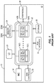
- FIG. 1 is a schematic diagram of an exemplary system-on-a-chip (SoC) 10 that includes a CPU-based system 12.
- the CPU-based system 12 includes a plurality of CPU blocks 14(1)-14(N) in this example, wherein 'N' is equal to any number of CPU blocks 14(1)-14(N) desired.
- each of the CPU blocks 14(1)-14(N) contains two CPUs 16(1), 16(2).
- the CPU blocks 14(1)-14(N) further contain shared Level 2 (L2) caches 18(1)-18(N), respectively.
- a shared Level 3 (L3) cache 20 is also provided for storing cached data that is used by any of, or shared among, each of the CPU blocks 14(1)-14(N).
- An internal system bus 22 is provided to enable each of the CPU blocks 14(1)-14(N) to access the shared L3 cache 20 as well as other shared resources.
- Other shared resources accessed by the CPU blocks 14(1)-14(N) through the internal system bus 22 may include a memory controller 24 for accessing a main, external memory (e.g., double-rate dynamic random access memory (DRAM) (DDR) provided in a dual in-line memory module (DIMM), as a non-limiting example), peripherals 26, other storage 28, an express peripheral component interconnect (PCI) (PCI-e) interface 30, a direct memory access (DMA) controller 32, and/or an integrated memory controller (IMC) 34.
- DRAM double-rate dynamic random access memory
- DIMM dual in-line memory module
- PCI-e express peripheral component interconnect
- DMA direct memory access
- IMC integrated memory controller
- CPU-based applications executing in the CPU-based system 12 in Figure 1 increase in complexity and performance
- memory capacity can be a constraint.
- providing additional memory capacity in a CPU-based system increases costs and area needed for memory on an integrated circuit (IC).
- IC integrated circuit
- SoC SoC 10
- adding additional memory capacity may increase the SoC packaging.
- Data compression may be employed to increase the effective memory capacity of a CPU-based system without increasing physical memory capacity. Data compression can also be employed to increase memory access bandwidth between a memory controller and memory.
- data for a write operation in the CPU-based system 12 in Figure 1 can be compressed, and the memory controller 24 may be configured to compress the data according to a defined compression algorithm. The compressed data is then written in compressed form at the data address in memory for the write operation.
- the memory controller 24 needs to be able to determine if the data stored at the accessed data address in memory is stored in compressed or uncompressed form.
- a data indicator may be provided that is associated with the data address in memory.
- the memory controller 24 can consult the data indicator for a read operation for a given data address to determine if the read data should be uncompressed.
- providing additional data indicators associated with the data addresses in memory increases memory size.
- the memory data bus width between the memory controller 24 and memory would have to be increased, which may be undesirable.
- WO2014/051625 discloses example methods, systems, and apparatus to dynamically select between memory error detection and memory error correction.
- DIMMs dual in-line memory modules
- ECC error correcting code
- the data indicator(s) may be stored in the DIMM without the need to provide additional data storage in the DIMM and increase the data width of the DIMM and/or the data bus width of the DIMM.
- Related memory controllers, memory systems, and methods are also disclosed. In this manner, additional memory is not required to be provided to store data indicators.
- Data indicators may be stored in an ECC storage unit in the DIMM for a variety of non-limiting applications.
- a data indicator may be stored in an ECC storage unit as a data indicator for indicating if data stored in memory is compressed or uncompressed.
- Another example where it may be desired to store a data indicator in an ECC storage unit in a DIMM may be to store cache coherency information in the DIMM used as a cache memory, such as whether each cache line of data in the DIMM is present on other processing nodes in the system.
- a dual in-line memory module that supports storage of a data indicator(s) in an error correcting code (ECC) storage unit dedicated to storing an ECC.
- the DIMM provides storage for data in a central processing unit (CPU)-based system.
- a memory controller provides an interface to the DIMM for read and write operations.
- the DIMM is configured in a plurality of burst data storage units.
- a burst data storage unit is a storage unit bit size in the DIMM for a burst data transaction according to a burst data length provided by the memory controller in the CPU-based system.
- a burst data length may be four (4) data line storage units in the DIMM, wherein each data line storage unit is sixty-four (64) data bit cells.
- the DIMM is also configured to provide a burst ECC storage unit striped over a plurality of ECC line storage units each corresponding to a data line storage unit.
- each ECC line storage unit includes an ECC byte storage unit comprising eight (8) data bit cells.
- the DIMM is seventy-two (72) bits wide (i.e., each data line storage unit being sixty-four (64) bit cells for storing sixty-four (64) data bits and an eight (8) bit cell ECC line storage unit for storing eight (8) ECC bits).
- each burst data storage unit can store two hundred fifty-six (256) bits of burst data (i.e., burst length of four (4) times sixty-four (64) bit data byte storage unit) and thirty-two (32) bits of a burst ECC word for the burst data (i.e., burst length of four (4) times eight (8) bit ECC byte storage unit).
- the DIMM is configured to receive a burst data word, a burst ECC word for the burst data word, and a data indicator for the burst data word. The DIMM is then configured to stripe the received burst data word across the burst data word storage unit in the burst data storage unit at a write data address for the write operation. The DIMM is also configured to stripe the received burst ECC word for the burst data word across the burst ECC storage unit in fewer bits than a number of data bit cells in the burst ECC storage unit.
- the DIMM can be configured to store at least one data indicator for the burst data word in the extra, leftover bit(s) in the burst ECC storage unit of the burst data storage unit, such that memory size does not have to be increased to store a data indicator(s).
- the memory data bus width of the DIMM does not have to be increased (e.g., beyond seventy-two (72) bits in the above referenced example) to avoid an increase in latency, because the data indicator can be written or read in the write or read operation for a burst data word in the DIMM as part of the ECC in the same burst cycle.
- a DIMM comprises a plurality of burst data storage units.
- Each burst data storage unit among the plurality of burst data storage units comprises a burst data word storage unit striped over a plurality of data line storage units totaling a burst length.
- Each data line storage unit among the plurality of data line storage units comprises sixty-four (64) data bit cells.
- Each burst data storage unit among the plurality of burst data storage units further comprises a burst ECC storage unit striped over a plurality of ECC line storage units.
- Each ECC line storage unit among the plurality of ECC line storage units corresponds to a data line storage unit, and comprises eight (8) data bit cells.
- the DIMM is configured to receive a write data address for a burst memory write request, and receive burst write data of a burst write data block length for the burst memory write request.
- the burst write data comprises a burst write data word, a burst ECC word for the burst write data word, and at least one data indicator for the burst write data word.
- the DIMM is further configured to stripe the received burst write data word across the burst data word storage unit at the received write data address.
- the DIMM is also configured to stripe the received burst ECC word for the burst write data word across the burst ECC storage unit in fewer bits than a number of data bit cells in the burst ECC storage unit at the received write data address.
- the DIMM is further configured to store the at least one data indicator for the burst write data word in the burst ECC storage unit of the burst data storage unit at the received write data address.
- a method of writing data to a DIMM in a CPU-based system comprises receiving a memory write request in a DIMM.
- the memory write request comprises a write data address and burst write data of a burst write data block length.
- the burst write data comprises a burst write data word, a burst ECC word for the burst write data word, and at least one data indicator for the burst write data word.
- the method also comprises striping the received burst write data word across a burst data word storage unit in a burst data storage unit at the received write data address in the DIMM.
- the DIMM comprises a plurality of burst data storage units.
- Each burst data storage unit among the plurality of burst data storage units comprises a burst data word storage unit striped over a plurality of data line storage units totaling a burst length.
- Each data line storage unit among the plurality of data line storage units comprises sixty-four (64) data bit cells.
- Each burst data storage unit among the plurality of burst data storage units further comprises a burst ECC storage unit striped over a plurality of ECC line storage units.
- Each ECC line storage unit among the plurality of ECC line storage units corresponds to a data line storage unit, and comprises eight (8) data bit cells.
- the method further comprises striping the received burst ECC word in the DIMM for the burst write data word across the burst ECC storage unit in fewer bits than a number of data bit cells in the burst ECC storage unit at the received write address.
- a memory system for a CPU-based system comprises a DIMM.
- the DIMM comprises a plurality of burst data storage units.
- Each burst data storage unit among the plurality of burst data storage units comprises a burst data word storage unit striped over a plurality of data line storage units totaling a burst length.
- Each data line storage unit among the plurality of data line storage units comprises sixty-four (64) data bit cells.
- Each burst data storage unit among the plurality of burst data storage units further comprises a burst ECC storage unit striped over a plurality of ECC line storage units.
- Each ECC line storage unit among the plurality of ECC line storage units corresponds to a data line storage unit, and comprises eight (8) data bit cells.
- the DIMM is configured to receive a burst memory write request comprising a write data address and burst write data of a burst write data block length.
- the burst write data comprises a burst write data word, a burst ECC word for the burst write data word, and at least one data indicator for the burst write data word.
- the DIMM is also configured to stripe the received burst write data word across the burst data word storage unit at the received write data address.
- the DIMM is further configured to stripe the received burst ECC word for the burst write data word across the burst ECC storage unit in fewer bits than a number of data bit cells in the burst ECC storage unit at the received write data address.
- the DIMM is further configured to store the at least one data indicator for the burst write data word in the burst ECC storage unit of the burst data storage unit at the received write data address.
- the memory system further comprises a memory controller.
- the memory controller is configured to receive a memory write request comprising the write data address and write data of a write data block length.
- the memory controller is configured to calculate one or more burst ECC words for the write data, each of the one or more burst ECC words having a length less than the number of data bit cells in the burst ECC storage unit, according to a defined ECC.
- the memory controller is also configured to construct one or more burst write data of the burst write data block length based on the write data.
- Each of the one or more burst write data comprises a burst write data word, a burst ECC word for the burst write data word, and at least one data indicator for the burst write data word.
- the memory controller is further configured to communicate the write data address and the one or more burst write data words to the DIMM to be stored at the write data address in the DIMM.
- a method of writing data to a memory system in a CPU-based system comprises receiving a memory write request comprising a write data address and write data of a write data block length.
- the method further comprises calculating one or more burst ECC words for the write data, each of the one or more burst ECC words having a length less than a number of data bit cells in a burst ECC storage unit, according to a defined ECC.
- the method also comprises constructing one or more burst write data of a burst write data block length based on the write data.
- Each of the one or more burst write data comprising a burst write data word, a burst ECC word for the burst write data word, and at least one data indicator for the burst write data word.
- the method further comprises communicating the write data address and one or more burst write data words to a DIMM to be stored at the write data address in the DIMM.
- the method also comprises receiving the memory write request in the DIMM.
- the memory write request comprises the write data address and the one or more burst write data of the burst write data block length, the one or more burst write data comprising a burst write data word, a burst ECC word for the burst write data word, and at least one data indicator for the burst write data word.
- the method further comprises striping the received burst write data word across a burst data word storage unit in a burst data storage unit at the received write data address in the DIMM.
- the DIMM comprises a plurality of burst data storage units.
- Each burst data storage unit among the plurality of burst data storage units comprises a burst data word storage unit striped over a plurality of data line storage units totaling a burst length.
- Each data line storage unit among the plurality of data line storage units comprises sixty-four (64) data bit cells.
- Each burst data storage unit among the plurality of burst data storage units comprises an ECC storage unit striped over a plurality of ECC line storage units, each ECC line storage unit among the plurality of ECC line storage units corresponding to a data line storage unit, and comprising eight (8) data bit cells.
- the method further comprises striping the received one or more burst ECC words in the DIMM for the burst write data word across the burst ECC storage unit in fewer bits than a number of data bit cells in the burst ECC storage unit at the received write data address.
- a data indicator is provided and associated with each data word in memory that can be written by a memory controller.
- the data indicator may be used to indicate if the memory controller compressed the written data word during a write operation.
- the data indicator can also be read and used by the memory controller.
- the memory controller may use the data indicator to determine if a read data word for a read operation was previously stored compressed, so that the read data word can be uncompressed.
- the aspects discussed herein of DIMMs that support storage of a data indicator(s) in an ECC storage unit dedicated to storing an ECC are not limited to storing data indicators to indicate data compression.
- FIG. 2 is a schematic diagram of an SoC 10' that includes an exemplary CPU-based system 12' having a plurality of CPU blocks 14(1)-14(N) similar to the CPU-based system 12 in Figure 1 .
- the CPU-based system 12' in Figure 2 includes some common components with the CPU-based system 12 in Figure 1 , which are noted by common element numbers between Figures 1 and 2 . For the sake of brevity, these elements will not be re-described.
- a memory controller 36 is provided in the CPU-based system 12' in Figure 2 .
- the memory controller 36 controls access to a system memory 38.
- the system memory 38 may comprise one or more double data rate (DDR) dynamic random access memories (DRAMs) 40(1)-40(R) (referred to hereinafter as "DRAM 40(1)-40(R)”), as a non-limiting example.
- DDR double data rate
- DRAM 40(1)-40(R) dynamic random access memories
- the memory controller 36 in this example employs memory bandwidth compression according to the aspects disclosed herein and below. Similar to the memory controller 24 of the CPU-based system 12 of Figure 1 , the memory controller 36 in the CPU-based system 12' in Figure 2 is shared by the CPU blocks 14(1)-14(N) through the internal system bus 22.
- Figure 3 To illustrate a more detailed schematic diagram of exemplary internal components of the memory controller 36 in Figure 2 , Figure 3 is provided.
- the memory controller 36 is provided on a separate semiconductor die 44 from semiconductor dies 46(1), 46(2) that contain the CPU blocks 14(1)-14(N) in Figure 2 .
- the memory controller 36 may be included in a common semiconductor die (not shown) with the CPU blocks 14(1)-14(N). Regardless of the die configurations, the memory controller 36 is provided such that the CPU blocks 14(1)-14(N) may make memory access requests via the internal system bus 22 to the memory controller 36, and receive data from memory through the memory controller 36.
- the memory controller 36 controls operations for memory accesses to the system memory 38, which is shown in Figures 2 and 3 as comprising DRAM 40(1)-40(R).
- the memory controller 36 includes a plurality of memory interfaces (MEM I/Fs) 48(1)-48(P) (e.g., DDR DRAM interfaces) used to service memory access requests (not shown).
- the memory controller 36 in this example includes a compression controller 50.
- the compression controller 50 controls compressing data stored to the system memory 38 and decompressing data retrieved from the system memory 38 in response to memory access requests from the CPU blocks 14(1)-14(N) in Figure 2 .
- the CPU blocks 14(1)-14(N) can be provided with a virtual memory address space greater than the actual capacity of memory accessed by the memory controller 36.
- the compression controller 50 can also be configured to perform bandwidth compression of information provided over the internal system bus 22 to the CPU blocks 14(1)-14(N).
- the compression controller 50 can perform any number of compression techniques and algorithms to provide memory bandwidth compression.
- a local memory 52 is provided for data structures and other information needed by the compression controller 50 to perform such compression techniques and algorithms.
- the local memory 52 is provided in the form of a static random access memory (SRAM) 54.
- SRAM static random access memory
- the local memory 52 is of sufficient size to be used for data structures and other data storage that may be needed for the compression controller 50 to perform compression techniques and algorithms.
- the local memory 52 may also be partitioned to contain a cache, such as a Level 4 (L4) cache, to provide additional cache memory for internal use within the memory controller 36.
- L4 controller 55 may also be provided in the memory controller 36 to provide access to the L4 cache.
- Enhanced compression techniques and algorithms may require a larger internal memory, as will be discussed in more detail below.
- the local memory 52 may provide 128 kilobytes (kB) of memory.
- an optional additional internal memory 56 can also be provided for the memory controller 36.
- the additional internal memory 56 may be provided as DRAM, as an example.
- the additional internal memory 56 can facilitate additional or greater amounts of storage of data structures and other data than in the local memory 52 for the memory controller 36 providing memory compression and decompression mechanisms to increase the memory bandwidth compression of the CPU-based system 12'.
- An internal memory controller 58 is provided in the memory controller 36 to control memory accesses to the additional internal memory 56 for use in compression. The internal memory controller 58 is not accessible or viewable to the CPU blocks 14(1)-14(N).
- the memory controller 36 in Figure 3 may perform memory bandwidth compression, including, in some aspects, zero-line compression.
- the local memory 52 can be used to store larger data structures used for such compression.
- memory bandwidth compression may reduce memory access latency and allow more CPUs 16(1), 16(2) or their respective threads to access a same number of memory channels while minimizing the impact to memory access latency.
- the number of memory channels may be reduced while achieving similar latency results compared to a greater number of memory channels if such compression was not performed by the memory controller 36, which may result in reduced system level power consumption.
- Each of the resources provided for memory bandwidth compression in the memory controller 36 in Figure 3 can be used individually or in conjunction with each other to achieve the desired balance among resources and area, power consumption, increased memory capacity through memory capacity compression, and increased performance through memory bandwidth compression.
- Memory bandwidth compression can be enabled or disabled, as desired. Further, the resources described above for use by the memory controller 36 can be enabled or disabled to achieve the desired tradeoffs among memory capacity and/or bandwidth compression efficiency, power consumption, and performance. Exemplary memory bandwidth compression techniques using these resources available to the memory controller 36 will now be discussed.
- One or more ECC bits may be included in a memory, such as in the CPU-based system 12 in Figure 1 , to perform ECC operations. However, it may also be desired to store at least one data indicator in association with a memory line for any number of reasons or purposes. For example, if a memory controller CPU-based system 12 is capable of performing data compression of stored data, the data indicator may be used to indicate whether the memory line is stored in compressed form or not. In this manner, when performing a memory access request to the system memory, a memory controller can check the data indicator associated with the memory line corresponding to the physical address to be addressed to determine if the memory line is compressed as part of processing of the memory access request.
- a data indicator stored in memory in association with a stored data word may be used for cache coherency to indicate whether the stored data is present in another memory in a CPU-based system.
- providing data indicators for memory lines in memory increases memory size.
- the memory data bus width between the memory controller and the memory may have to be increased, which may be undesirable, or latency may be increased.
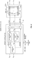
- Figure 4 is an exemplary memory system 130 that includes a memory controller 132, which may be the memory controller 36 in Figure 2 as an example.
- the memory system 130 can be provided in a CPU-based system, including the CPU-based system 12' discussed above and illustrated in Figure 2 .
- a DIMM 134 is provided to store memory data.
- the memory controller 132 and DIMM 134 are typically powered in the same voltage domain (shown as Vdd and Vss in Figure 4 ).
- the memory controller 132 is communicatively coupled to the DIMM 134 to provide memory access requests for read and write operations to the DIMM 134.
- the memory controller 132 is configured to receive memory read requests 136R and memory write requests 136W over a system bus 138.
- a memory read request 136R includes a read data address to be read in the DIMM 134.
- a memory write request 136W includes a write data address and write data to be written at the write data address in the DIMM 134.
- the memory controller 132 is configured to determine if the write data can be compressed, the memory controller 132 can compress the write data to be stored in the DIMM 134 according to a compression algorithm. Similar to the examples discussed above, the memory controller 132 is configured to provide at least one data indicator to the DIMM 134 as part of a write operation so that the DIMM 134 can provide the at least one data indicator to the memory controller 132 during a read operation.
- the data indicator may be used to indicate if the read data was stored compressed or uncompressed.
- the DIMM 134 is configured to support storage of at least one data indicator in an ECC storage unit dedicated to storing an ECC. In this manner, additional memory is not required to be provided to store the data indicator(s).
- the memory controller 132 includes a controller 140, which may be similar to the compression controller 50 in the memory controller 36 in Figure 3 .
- the controller 140 is configured to receive write data for a memory write request 136W. Regardless, the write data is provided as a data input (Din) to an ECC circuit 142.
- the ECC circuit 142 includes an ECC encoder 144E that is configured to calculate an ECC word for the write data.
- the write data, the ECC word for the write data, and a data indicator set by the controller 140 is communicated through a memory interface (I/F) 146 over a memory bus 148 to the DIMM 134 to be stored in conjunction with each other.
- I/F memory interface
- the controller 140 is configured to provide the command (e.g., write command) and data address (e.g., a write data address) as cmd/addr information along with the write data on the data input (Din) through the memory interface 146 to the DIMM 134.
- the memory interface 146 may be or may be similar to the memory interface 48 in the memory controller 36 in Figure 3 .
- the memory controller 132 may break up the write data into multiple burst write data words communicated to the DIMM 134 to be stored.
- the DIMM 134 in Figure 4 may be seventy-two (72) bits wide.
- the DIMM 134 in Figure 4 includes a plurality of data line storage units 150(0)-150(U) each comprising sixty-four (64) data bit cells 152. Multiple data line storage units 150(0)-150(U) may be partitioned in the DIMM 134 to provide a burst data storage unit.
- a burst data storage unit is a storage unit bit size in the DIMM 134 for a burst data transaction according to the burst data length.
- a burst data length may be equal to the size of four (4) data line storage units 150(0)-150(U) in the DIMM 134, wherein each data line storage unit 150(0)-150(U) is a data byte storage unit comprising sixty-four (64) data bit cells 152.
- a data burst is 32 bytes (i.e., 64 bits in a data line storage unit 150 times 4 data lines).
- the data word size for the memory system 130 is sixty-four (64) bytes
- eight (8) data line storage units 150(0)-150(U) will be employed in the DIMM 134 to store this data word totaling 64 bytes, which is provided in two data bursts of 32 bytes each.
- an ECC line storage unit 154(0)-154(U) is also provided in the DIMM 134 for each data line storage units 150(0)-150(U).
- the ECC line storage units 154(0)-154(U) are configured to store one or more ECC words corresponding to a data word striped over one or more data line storage units 150(0)-150(U) in the DIMM 134.
- the DIMM 134 is configured to stripe a calculated ECC for write data over the plurality of ECC line storage units 154(0)-154(U), if a burst data word is larger than the size of a single data line storage unit 150.
- a burst data word is 32 bytes and thus an ECC code for a data word can be striped by the DIMM 134 over 32 bits over four (4) ECC line storage units 154(0)-154(U) of eight (8) bits each (i.e., 32 bits) corresponding to four (4) data line storage units 150(0)-150(U).
- a plurality of data indicator units 156(0)-156(R) are provided in the DIMM 134 to provide a storage unit to store a data indicator that can be used to provide an indication about stored data words. Because as discussed below, the data indicator units 156(10)-156(R) are provided as part of the ECC line storage units 154(0)-154(U) based on the ECC bit error correction code selected for use, additional bits of storage are not required in the DIMM 134 to store the data indicator units 156(0)-156(R).
- each data indicator unit 156(0)-156(R) may differ from the number of data line storage units 150(0)-150(U) if the data burst length is such that stored data words are larger than the size of the data line storage units 150(0)-150(U) in the DIMM 134, because only one data indicator unit 156 is needed for each single data word.
- each data indicator unit 156(0)-156(R) can consist of one (1) bit to store a data indicator that simply indicates one of two states about the corresponding stored data word.
- the data indicator units 156(0)-156(R) can be configured to store multiple bits to also allow storage of multiple data indicators for given data word to be encoded and stored in the DIMM 134 in association with the given data word.
- the controller 140 is also configured to receive a memory read request 136R comprising a read data address over the system bus 138 to perform a read operation.
- the controller 140 provides the read operation and the read data address to the DIMM 134 through the cmd/addr information for the read data to be accessed by the DIMM 134 at the read address.
- the DIMM 134 provides the read data, the ECC associated with the read data, and the at least one data indicator associated with the read data as output data (Dout) to the memory interface 146 of the memory controller 132.
- the ECC associated with the read data is provided to an ECC decoder 144D in the ECC circuit 142 to determine if the read data contains a bit error(s).
- the ECC decoder 144D corrects any detected bit error(s), if possible, depending on the ECC bit error correction code employed by the memory controller 132.
- the bit error(s) is communicated to the controller 140 as a correction error signal (corr_er).
- the controller 140 can use the received data indicator(s) to determine if the read data is compressed or uncompressed. If compressed, the controller 140 decompresses the read data to provide the read data on the system bus 138 to the requestor that issued the memory read request 136R.
- Figure 5 is a diagram of an exemplary data partitioning of the data line storage units 150(0)-150(U) in the DIMM 134 of the memory system 130 in Figure 4 to illustrate an example of storing data indicators as part of an ECC line storage unit 154.
- the DIMM 134 is partitioned into a plurality of burst data storage units 160(0)-160(3).
- Four (4) burst data storage units 160(0)-160(3) of the DIMM 134 are shown in Figure 5 , which may be the size of a cache line for example (i.e., 256 bytes).
- each burst data storage unit 160(0)-160(3) is comprised of four (4) data line storage units 150(0)-150(3) to allow for a burst data word stored therein to be thirty-two (32) bytes in length.
- data line storage units 150(0)-150(15) are shown in the DIMM 134, because only four (4) burst data storage units 160(0)-160(3) are shown.
- a data word in a CPU-based system in which the memory system 130 in Figure 4 is provided is sixty-four (64) bytes, so each data word can be stored as two (2) burst data words in two (2) burst data storage units 160(0)-160(1) each able to store thirty-two (32) bytes each.
- each burst data word storage unit 160 is striped over four (4) data line storage units 150(0)-150(3) totaling the burst length, with each data line storage unit 150 each comprising sixty-four (64) data bit cells.
- the DIMM 134 is double data rate (DDR) clocked meaning that the DIMM 134 is clocked on both the rising and falling edge of a clock signal.
- DDR double data rate
- a clock signal status is shown to explain how the data line storage units 150(0)-150(15) are accessed by the DIMM 134 sequentially over time, as shown by a time arrow 158.
- the data line storage unit 150(0) is accessed on the rising edge of the clock signal in cycle '0' (i.e., clockO-r).
- the data line storage unit 150(1) is accessed on the falling edge of the clock signal in cycle '0" (clock0-f), and so on.
- the DIMM 134 is also partitioned into a plurality of burst ECC storage units 162 that are each capable of storing a burst ECC word.
- burst ECC storage units 162(0)-162(3) of the DIMM 134 are shown in Figure 5 , wherein each burst ECC storage unit 162(0)-162(3) is associated with a respective burst data storage unit 160(0)-160(3).
- each burst ECC storage unit 162(0)-162(3) is comprised of four (4) ECC line storage units 154(0)-154(3) to provide for each burst ECC word to be thirty-two (32) bits in length, since each ECC line storage unit 154 is comprised of eight (8) data bits.
- each ECC line storage unit 154 is comprised of eight (8) data bits.
- only sixteen (16) ECC line storage units 154(0)-154(15) are shown in the DIMM 134, because only four (4) burst data storage units 160(0)-160(3) are shown.
- a data word in the CPU-based system in which the memory system 130 in Figure 4 is provided is sixty-four (64) bytes, so each data word is comprised of two (2) burst data storage units 150(0)-150(1) each able to store thirty-two (32) bytes each.
- each burst ECC storage unit 162 is striped over four (4) ECC line storage units 154(0)-154(3) totaling the burst length, with each ECC line storage unit 154 each comprising eight (8) data bit cells to allow for a total of thirty-two (32) ECC bits to be stored as a burst ECC word for a burst data word.
- an ECC bit error correction code is chosen that provides for an ECC bit size to be less than thirty-two (32) bits for each burst data word.
- the chosen ECC bit error correction code be able to provide a highly capable bit error detection and correction scheme, where possible, to maintain the integrity of data words stored in the DIMM 134.
- RS code Reed-Solomon (RS) bit error correction code
- the RS code is a known ECC bit error correction code that can be employed according to the partition of the DIMM 134 shown in Figure 5 .
- the RS code of ⁇ 48, 43 ⁇ with a hamming distance of six (6) can be configured to allow the memory controller 132 to correct a single or two (2) data symbols 168 / check symbols 170 errors per code word 166 and can detect errors in three (3) data symbols 168 / check symbols 170 errors per code word 166.
- the RS code can be configured to allow the memory controller 132 to correct a single (1) data symbol 168 / check symbol 170 errors per code word 166 and can detect errors in four (4) data symbols 168 / check symbols 170 errors per code word 166.
- the DIMM 134 may be configured in 4-bit width DRAM chips.
- the ability to detect bit errors in multiple adjacent bit symbols i.e., data symbols 168 and/or check symbols 170 may be useful for detecting common types of memory failures, as will be described in more detail below with regard to Figures 9-14 .
- the burst ECC word for a burst data word can be striped across the burst ECC storage unit 162 in the DIMM 134 in fewer bits than a number of data bit cells in the burst ECC storage unit 162, to provide for the additional, unused extra bits 172.
- These extra bits 172 as shown in the DIMM 134 in Figure 5 are thus unused, and thus can be used to store a data indicator(s) for the burst data word stored in a code word 166.
- One or more of the four (4) extra bits 172 per data word of sixty-four (64) bytes over two (2) code words 166 in the DIMM 134 can be used.
- the data indicator(s) may be encoded over multiple extra bits 172. For example, with four (4) extra bits 172 per data word in this example, fifteen (15) different states about the data word could be encoded.
- FIG. 6 is a diagram illustrating more exemplary detail of the DIMM 134 that can be provided in the memory system 130 in Figure 4 and partitioned for data storage by the memory controller 132 according to the data partitioning shown in Figure 5 .
- the DIMM 134 is comprised of a plurality of DIMM chips 178(0)-178(X). In this example, nine (9) DIMM chips 178(0)-178(8) are included in the DIMM 134.
- a physical DIMM connector 180 is provided to interface the DIMM 134 and the DIMM chips 178(0)-178(8) therein to the memory bus 148 (see Figure 4 ). Exemplary detail for one DIMM chip 178 is shown in Figure 6 .
- each DIMM chip 178(0)-178(8) is addressable in thirty-two (32) rows (R1-R5) and thirty-two (32) columns (C1-C5) to address sixteen (16) bits of striped data in two (2) adjacent rows of the DIMM 134 in a cell matrix 181.
- nine (9) DIMM chips 178(0)-178(8) can store 128 bits, which is two (2) data line storage units 150(0)-150(1).
- a write data word provided to the DIMM 134 is striped across the DIMM chips 178(0)-178(8) on data inputs (Din) for the DIMM chips 178(0)-178(8).
- a read/write (R/W) signal is provided to the DIMM chips 178(0)-178(8) as cmd/addr information from the memory controller 132 to indicate either a memory read operation 136R or a memory write operation 136W.
- the access data stored in the DIMM chips 178(0)-178(8) is provided on respective data outputs (Dout) to be provided to the memory controller 132.
- the memory controller 132 in Figure 4 is configured to perform memory read and write operations in the DIMM 134 using a bit error correction code that allows for at least one extra bit(s) 172 to be provided for each data word stored therein.
- Figure 7A is a flowchart illustrating an exemplary process 190 of the memory controller 132 in Figure 4 processing a write operation to store a received data word in the DIMM 134 compatible with the exemplary data partitioning of the DIMM 134 in Figure 5 .
- Figure 7B is a flowchart illustrating an exemplary process 210 of the DIMM 134 in Figure 4 striping a burst write data word and a burst ECC word for the burst write data word in a burst data storage unit 160 and burst ECC storage unit 162 along with a data indicator(s) .
- the process 190 starts by the memory controller 132 in Figure 4 receiving a memory write request 136W comprising the write data address and the write data of a write data block length (block 192).
- the memory controller 132 may optionally compress the write data if the write data can be compressed according to a defined compression code (block 194).
- the memory controller 132 then calculates one or more burst ECC words for the write data, each of the one or more burst ECC words having a length less than a number of data bit cells in the burst ECC storage unit 162 in the DIMM 134, according to a defined ECC (block 196).
- the memory controller 132 then constructs one or more burst write data of a burst write data block length based on the write data, each of the one or more burst write data comprising a burst write data word and a burst ECC word for the burst write data word, and at least one data indicator for the burst write data word (block 198).
- the memory controller 132 then communicates the write operation and write data address as cmd/addr information and the one or more burst write data words as input data (Din) to the DIMM 134 to be stored at the write data address in the DIMM 134 (block 200).
- the process 210 in the DIMM 134 involves receiving the write data address for the memory write request 136W from the memory controller 132 (block 212).
- the DIMM 134 receives burst write data of a burst write data block length for the memory write request 136W, the burst write data comprising a burst write data word, a burst ECC word for the burst write data word, and at least one data indicator for the burst write data word.
- the DIMM 134 then stripes the received burst write data word across the burst data storage unit 160 at the received write data address (block 214).
- the DIMM 134 also stripes the received burst ECC word for the burst write data word across the burst ECC storage unit 162 in fewer bits than a number of data bit cells in the burst ECC storage unit 162, in the burst data storage unit 160 at the received write data address (block 216).
- the DIMM 134 stores the at least one data indicator for the burst write data word in the burst ECC storage unit 162 at the received write data address (block 218).
- Figure 8A is a flowchart illustrating an exemplary process 220 of the memory controller 132 in Figure 4 processing a read operation to request and a receive a read data word from the DIMM 134 compatible with the exemplary data partition of the DIMM 134 in Figure 5 .
- Figure 8B is a flowchart illustrating an exemplary process 240 of the DIMM 134 in Figure 4 accessing a burst read data word and a burst ECC word for the burst read data word in a burst data storage unit 160 along with a data indicator(s) .
- the process 220 for a memory read operation in the memory controller 132 starts by the memory controller 132 receiving a memory read request 136R comprising a read data address of a memory block in the DIMM 134 (block 222).
- the memory controller 132 then communicates the memory read request 136R to the DIMM 134 by providing the read operation and read data address as cmd/addr information to the DIMM 134, as shown in Figure 4 (block 224).
- the DIMM 134 processes the read operation (discussed below in Figure 8B ), the DIMM 134 communicates back the burst read data from the DIMM 134 to the memory controller 132.
- the memory controller 132 receives one or more burst read data from the DIMM 134 stored at the read data address in the DIMM 134 (block 226).
- the one or more burst read data each comprise a burst read data word, a burst ECC word for the burst read data word, and a data indicator(s) for the burst read data word.
- the memory controller 132 then calculates one or more burst ECC words for the one or more received burst read data for a read data word to perform error detection and correction, if necessary (block 228).
- the memory controller 132 compares the calculated one or more burst ECC words for the one or more burst read data to determine if the one or more burst read data words has an error(s), which may be correctable and corrected (block 230). For example, if the memory controller 132 is configured to perform data compression and use the data indicator(s) to indicate whether data is stored in compressed or uncompressed form, the memory controller 132 can optionally be configured to determine if the one or more burst read data words is compressed or uncompressed based on the data indicator(s) received for the one or more burst read data words (block 232).
- the memory controller 132 can be configured to optionally decompress the one or more burst read data words if the data indicator(s) indicates that the one or more burst read data words are compressed (block 234). The memory controller 132 then communicates the one or more burst read data words from the DIMM 134 onto the system bus 138 (block 236).
- the DIMM 134 when the DIMM 134 receives the memory read request 136R from the memory controller 132 that contains the read data address (block 242), the DIMM 134 accesses the data word stored at the read data address (block 244).
- the DIMM 134 retrieves one or more burst read data stored at the read data address in the DIMM 134 (block 244).
- the DIMM 134 then communicates the one or more burst read data stored at the read data address to the memory controller 132 (block 246).
- Each of the one or more burst read data comprises a burst read data word, a burst ECC word for the burst read data word, and at least one data indicator for the burst read data word.
- Figure 9 is a diagram of the DIMM 134 in Figure 6 according to the exemplary data partition in Figure 5 illustrating an exemplary single memory bit cell 250 failure in a data symbol 168 of a code word 166.
- the memory controller 132 can detect and correct this bit error as part of its ECC circuit 142 operation. Even if other bit errors were present in other data symbols 168 or check symbols 170, a single bit error in such other data symbols 168 or check symbols 170 could be detected and corrected.
- Figure 10 is a diagram of the DIMM 134 in Figure 6 according to the exemplary data partition in Figure 5 configured in eight (8) bit width and illustrating an exemplary memory bank or row failure.
- the code word 166 in Figure 10 is shown as having a bit failure in a row or bank 252.
- a failed memory row or bank 252 will appear as having at least one bit error in at least three (3) adjacent data symbols 168 or check symbols 170, because a bit error in two (2) adjacent data symbols168 or check symbols 170 could be a column or row failure with an eight (8) bit width.
- an exemplary memory bank or row failure 254 will appear in four (4) or more adjacent bit cells in adjacent data symbols 168 or check symbols 170 having a bit error.
- Figure 12 is a diagram of the DIMM 134 in Figure 6 according to the exemplary data partition in Figure 5 illustrating an exemplary memory column 256 failure.
- a failed memory column 256 will appear as having a bit error in the same column 256 in at least two (2) adjacent data symbols 168 or check symbols 170.
- Figure 13 is a diagram of the DIMM 134 in Figure 6 according to the exemplary data partition in Figure 5 illustrating an exemplary bit lane 258 failure in the DIMM 134.
- a bit lane 258 failure can be detected based on at least one bit error being detecting in a bit lane 258 in at least two (2) adjacent symbols in the data symbols 168 and/or check symbols 170 based on a bit error correction code.
- an exemplary four (4) bit word 260 failure will appear as four (4) adjacent bit cells, which cross adjacent symbols among the data symbols 168 and/or check symbols 170.
- DIMMs supporting storage of a data indicator(s) in an ECC storage unit dedicated to storing an ECC may be provided in or integrated into any processor-based device. Examples, without limitation, include a set top box, an entertainment unit, a navigation device, a communications device, a fixed location data unit, a mobile location data unit, a mobile phone, a cellular phone, a computer, a portable computer, a desktop computer, a personal digital assistant (PDA), a monitor, a computer monitor, a television, a tuner, a radio, a satellite radio, a music player, a digital music player, a portable music player, a digital video player, a video player, a digital video disc (DVD) player, and a portable digital video player.
- PDA personal digital assistant
- Figure 15 illustrates an example of a processor-based system 270 that can employ the SoC 10' of Figure 2 with the memory system 130 including the memory controller 132 and the DIMM 134 (shown as DIMMs 134(0)-134(X)) of Figure 4 .
- the processor-based system 270 includes one or more CPUs 272, each including one or more processors 274.
- the CPU(s) 272 may have cache memory 276 coupled to the processor(s) 274 for rapid access to temporarily stored data.
- the cache memory 276 could include a memory system like the memory system 130 in Figure 4 .
- the CPU(s) 272 is coupled to a system bus 278 and can intercouple devices included in the processor-based system 270.
- the CPU(s) 272 communicates with these other devices by exchanging address, control, and data information over the system bus 278.
- the CPU(s) 272 can communicate bus transaction requests to a memory controller 280 as an example of a slave device.
- a memory controller 280 as an example of a slave device.
- multiple system buses 278 could be provided.
- Other devices can be connected to the system bus 278. As illustrated in Figure 15 , these devices can include a memory system 281, one or more input devices 282, one or more output devices 284, one or more network interface devices 286, and one or more display controllers 288, as examples.
- the memory system 281 can include the memory system 130 in Figure 4 as an example.
- the input device(s) 282 can include any type of input device, including but not limited to input keys, switches, voice processors, etc.
- the output device(s) 284 can include any type of output device, including but not limited to audio, video, other visual indicators, etc.
- the network interface device(s) 286 can be any devices configured to allow exchange of data to and from a network 290.
- the network 290 can be any type of network, including but not limited to a wired or wireless network, a private or public network, a local area network (LAN), a wide local area network, wireless local area network, BLUETOOTH (BT), and the Internet.
- the network interface device(s) 286 can be configured to support any type of communications protocol desired.
- the memory system 281 can include the DIMMs 134(0)-134(X).
- the CPU(s) 272 may also be configured to access the display controller(s) 288 over the system bus 278 to control information sent to one or more displays 292.
- the display controller(s) 288 sends information to the display(s) 292 to be displayed via one or more video processors 294, which process the information to be displayed into a format suitable for the display(s) 292.
- the display(s) 292 can include any type of display, including but not limited to a cathode ray tube (CRT), a liquid crystal display (LCD), a light emitting diode (LED) display, a plasma display, etc.
- DSP Digital Signal Processor
- ASIC Application Specific Integrated Circuit
- FPGA Field Programmable Gate Array
- a processor may be a microprocessor, but in the alternative, the processor may be any conventional processor, controller, microcontroller, or state machine.
- a processor may also be implemented as a combination of computing devices, e.g., a combination of a DSP and a microprocessor, a plurality of microprocessors, one or more microprocessors in conjunction with a DSP core, or any other such configuration.
- RAM Random Access Memory
- ROM Read Only Memory
- EPROM Electrically Programmable ROM
- EEPROM Electrically Erasable Programmable ROM
- registers a hard disk, a removable disk, a CD-ROM, or any other form of computer readable medium known in the art.
- An exemplary storage medium is coupled to the processor such that the processor can read information from, and write information to, the storage medium.
- the storage medium may be integral to the processor.
- the processor and the storage medium may reside in an ASIC.
- the ASIC may reside in a remote station.
- the processor and the storage medium may reside as discrete components in a remote station, base station, or server.
- data, instructions, commands, information, signals, bits, symbols, and chips that may be referenced throughout the above description may be represented by voltages, currents, electromagnetic waves, magnetic fields or particles, optical fields or particles, or any combination thereof.
- the previous description of the disclosure is provided to enable any person skilled in the art to make or use the disclosure.
- Various modifications to the disclosure will be readily apparent to those skilled in the art, and the generic principles defined herein may be applied to other variations without departing from the scope of the disclosure.
- the disclosure is not intended to be limited to the examples and designs described herein, but is to be accorded the widest scope consistent with the principles and novel features disclosed herein.
Landscapes
- Engineering & Computer Science (AREA)
- Theoretical Computer Science (AREA)
- Physics & Mathematics (AREA)
- Quality & Reliability (AREA)
- General Engineering & Computer Science (AREA)
- General Physics & Mathematics (AREA)
- Probability & Statistics with Applications (AREA)
- Techniques For Improving Reliability Of Storages (AREA)
- Detection And Correction Of Errors (AREA)
Claims (17)
- Module de mémoire à double rangée en ligne, DIMM, (134), comprenant :une pluralité d'unités de stockage de données en rafales (160) ;chaque unité de stockage de données en rafales parmi la pluralité d'unités de stockage de données en rafales comprenant :une unité de stockage de mots de données en rafales (160) répartie sur une pluralité d'unités de stockage de lignes de données totalisant une longueur de rafales, chaque unité de stockage de lignes de données parmi la pluralité d'unités de stockage de lignes de données comprenant soixante-quatre (« 64 ») cellules de bits de données ; etune unité de stockage de code correcteur d'erreurs, ECC, en rafales, répartie sur une pluralité d'unités de stockage de lignes de codes ECC (154(0)-156(U)), chaque unité de stockage de lignes de codes ECC parmi la pluralité d'unités de stockage de lignes de codes ECC (154(0)-156(U)) correspondant à une unité de stockage de lignes de données, chaque unité de stockage de lignes de codes ECC comprenant huit (« 8 ») cellules de bits de données ; etdans lequel le module DIMM (134) est configuré de manière à :recevoir (212) une adresse de données d'écriture pour une demande d'écriture mémoire en rafales (136W) ;recevoir (212) des données d'écriture en rafales d'une longueur de bloc de données d'écriture en rafales pour la demande d'écriture mémoire en rafales (136W), les données d'écriture en rafales comprenant un mot de données d'écriture en rafales, un mot de code ECC en rafales pour le mot de données d'écriture en rafales, et au moins un indicateur de données pour le mot de données d'écriture en rafales ;répartir par bandes (214) le mot de données d'écriture en rafales reçu à travers l'unité de stockage de mots de données en rafales (160) à l'adresse de données d'écriture reçue ;répartir par bandes (216) le mot de code ECC en rafales reçu pour le mot de données d'écriture en rafales à travers l'unité de stockage de codes ECC en rafales (162) dans moins de bits qu'un nombre de cellules de bits de données dans l'unité de stockage de codes ECC en rafales (162) à l'adresse de données d'écriture reçue ; etstocker (218) ledit au moins un indicateur de données pour le mot de données d'écriture en rafales dans l'unité de stockage de codes ECC en rafales (162) de l'unité de stockage de données en rafales à l'adresse de données d'écriture reçue.
- Module DIMM (134) selon la revendication 1, dans lequel ledit au moins un indicateur de données pour le mot de données d'écriture en rafales est constitué d'un indicateur de données à un seul bit ;
dans lequel le module DIMM (134) est configuré de manière à stocker l'indicateur de données à un seul bit pour le mot de données d'écriture en rafales dans un seul bit de l'unité de stockage de codes ECC en rafales (162) de l'unité de stockage de données en rafales à l'adresse de données d'écriture reçue ; ou
dans lequel ledit au moins un indicateur de données pour le mot de données d'écriture en rafales est constitué d'un indicateur de données à bits multiples ; dans lequel le module DIMM (134) est configuré de manière à stocker l'indicateur de données à bits multiples pour le mot de données d'écriture en rafales dans de multiples bits de l'unité de stockage de codes ECC en rafales (162) de l'unité de stockage de données en rafales à l'adresse de données d'écriture reçue. - Module DIMM (134) selon la revendication 1, dans lequel le module DIMM (134) est configuré de manière à répartir par bandes le mot de code ECC en rafales reçu pour le mot de données d'écriture en rafales à travers l'unité de stockage de codes ECC en rafales (162) dans au moins deux bits de moins que le nombre de cellules de bits de données dans l'unité de stockage de codes ECC en rafales (162) à l'adresse de données d'écriture reçue.
- Module DIMM (134) selon la revendication 1, configuré en outre de manière à :recevoir une demande de lecture de mémoire (136R) comprenant une adresse de données de lecture ;accéder à l'adresse de données de lecture en vue de récupérer une ou plusieurs données de lecture en rafales stockées à l'adresse de données de lecture dans le module DIMM (134) ; etcommuniquer ladite une ou lesdites plusieurs données de lecture en rafales stockées à l'adresse de données de lecture à un contrôleur de mémoire, ladite une ou lesdites plusieurs données de lecture en rafales comprenant chacune un mot de données de lecture en rafales, un mot de code ECC en rafales pour le mot de données de lecture en rafales, et ledit au moins un indicateur de données pour le mot de données de lecture en rafales.
- Module DIMM (134) selon la revendication 1, dans lequel le module DIMM (134) est configuré de manière à recevoir ledit au moins un indicateur de données pour le mot de données d'écriture en rafales indiquant si le mot de données d'écriture en rafales est compressé.
- Module DIMM (134) selon la revendication 1, dans lequel chaque unité de stockage de données en rafales parmi la pluralité d'unités de stockage de données en rafales comprend l'unité de stockage de mots de données en rafales (160) répartie sur quatre unités de stockage de lignes de données totalisant la longueur de rafales.
- Module DIMM (134) selon la revendication 1, intégré dans un circuit intégré, IC, ou dans lequel le module DIMM (134) est intégré dans un dispositif sélectionné à partir du groupe constitué par : un boîtier décodeur ; une unité de divertissement ; un dispositif de navigation ; un dispositif de communication ; une unité de données de localisation fixe ; une unité de données de localisation mobile ; un téléphone mobile ; un téléphone cellulaire ; un ordinateur ; un ordinateur portable ; un ordinateur de bureau ; un assistant numérique personnel, PDA ; un moniteur ; un moniteur d'ordinateur ; un téléviseur ; un syntoniseur ; une radio ; une radio satellite ; un lecteur de musique ; un lecteur de musique numérique ; un lecteur de musique portable ; un lecteur vidéo numérique ; un lecteur vidéo ; un lecteur de disque vidéo numérique, DVD ; et un lecteur vidéo numérique portable.
- Procédé (210) d'écriture de données dans un module de mémoire à double rangée en ligne, DIMM (134), dans un système à base d'unité centrale de traitement, CPU, comprenant les étapes ci-dessous consistant à :recevoir (212) une demande d'écriture en mémoire (136W) dans un module DIMM (134), la demande d'écriture en mémoire (136W) comprenant une adresse de données d'écriture et des données d'écriture en rafales d'une longueur de bloc de données d'écriture en rafales, les données d'écriture en rafales comprenant un mot de données d'écriture en rafales, un mot de code correcteur d'erreurs, ECC, en rafales pour le mot de données d'écriture en rafales, et au moins un indicateur de données pour le mot de données d'écriture en rafales ;répartir par bandes (214) le mot de données d'écriture en rafales reçu à travers une unité de stockage de mots de données en rafales (160) dans une unité de stockage de données en rafales à l'adresse de données d'écriture reçue dans le module DIMM (134), le module DIMM (134) comprenant :
une pluralité d'unités de stockage de données en rafales, chaque unité de stockage de données en rafales parmi la pluralité d'unités de stockage de données en rafales comprenant :une unité de stockage de mots de données en rafales (160) répartie sur une pluralité d'unités de stockage de lignes de données totalisant une longueur de rafales, chaque unité de stockage de lignes de données parmi la pluralité d'unités de stockage de lignes de données comprenant soixante-quatre (« 64 ») cellules de bits de données ; etune unité de stockage de codes ECC en rafales (162) répartie sur une pluralité d'unités de stockage de lignes de codes ECC (154(0)-156(U)), chaque unité de stockage de lignes de codes ECC parmi la pluralité d'unités de stockage de lignes de codes ECC (154(0)-156(U)) correspondant à une unité de stockage de lignes de données, chaque unité de stockage de lignes de codes ECC comprenant huit (« 8 ») cellules de bits de données ;répartir par bandes (216) le mot de code ECC en rafales reçu dans le module DIMM (134) pour le mot de données d'écriture en rafales à travers l'unité de stockage de codes ECC en rafales (162) dans moins de bits qu'un nombre de cellules de bits de données dans l'unité de stockage de codes ECC en rafales (162) à l'adresse de données d'écriture reçue ; etstocker (218) ledit au moins un indicateur de données pour le mot de données d'écriture en rafales dans l'unité de stockage de codes ECC en rafales (162) de l'unité de stockage de données en rafales à l'adresse de données d'écriture reçue. - Système de mémoire (130) pour un système à base d'unité centrale de traitement, CPU, comprenant :un module de mémoire à double rangée en ligne, DIMM, (134) selon l'une quelconque des revendications 1 à 7, et comprenant en outre :un contrôleur de mémoire (132) configuré de manière à :recevoir une demande d'écriture en mémoire (136W) comprenant l'adresse de données d'écriture et des données d'écriture d'une longueur de bloc de données d'écriture ;calculer un ou plusieurs mots de code ECC en rafales pour les données d'écriture, chaque mot parmi ledit un ou lesdits plusieurs mots de code ECC en rafales présentant une longueur inférieure au nombre de cellules de bits de données dans l'unité de stockage de codes ECC en rafales (162), conformément à un code ECC défini ;construire une ou plusieurs données d'écriture en rafales de la longueur de bloc de données d'écriture en rafales sur la base des données d'écriture, chacune parmi ladite une ou lesdites plusieurs données d'écriture en rafales comprenant un mot de données d'écriture en rafales, un mot de code ECC en rafales pour le mot de données d'écriture en rafales, et au moins un indicateur de données pour le mot de données d'écriture en rafales ; etcommuniquer l'adresse de données d'écriture et ledit un ou lesdits plusieurs mots de données d'écriture en rafales au module DIMM (134) à des fins de stockage à l'adresse de données d'écriture dans le module DIMM (134).
- Système de mémoire (130) selon la revendication 9, dans lequel le contrôleur de mémoire (132) comprend en outre un codeur de code ECC configuré de manière à calculer ledit un ou lesdits plusieurs mots de code ECC en rafales pour les données d'écriture, chaque mot dudit un ou desdits plusieurs mots de code ECC en rafales présentant la longueur inférieure au nombre de cellules de bits de données dans l'unité de stockage de codes ECC en rafales (162), selon le code ECC défini.
- Système de mémoire (130) selon la revendication 9, dans lequel :le contrôleur de mémoire (132) est en outre configuré de manière à :recevoir une demande de lecture de mémoire (136R) comprenant une adresse de données de lecture d'un bloc de mémoire dans le module DIMM (134) ;communiquer la demande de lecture de mémoire (136R) au module DIMM (134) ;recevoir une ou plusieurs données de lecture en rafales en provenance du module DIMM (134), stockées à l'adresse de données de lecture dans le module DIMM (134), ladite une ou lesdites plusieurs données de lecture en rafales comprenant chacune un mot de données de lecture en rafales, un mot de code ECC en rafales pour le mot de données de lecture en rafales, et ledit au moins un indicateur de données pour le mot de données de lecture en rafales ;calculer ledit un ou lesdits plusieurs mots de code ECC en rafales pour ladite une ou lesdites plusieurs données de lecture en rafales ;comparer ledit un ou lesdits plusieurs mots de code ECC en rafales calculés pour ladite une ou lesdites plusieurs données de lecture en rafales en vue de déterminer si ladite une ou lesdites plusieurs données de lecture en rafales présentent une erreur de bit ; etcommuniquer ladite une ou lesdites plusieurs données de lecture en rafales à partir du module DIMM (134), sur un bus ; etle module DIMM (134) est en outre configuré de manière à :recevoir la demande de lecture de mémoire (136R) comprenant l'adresse de données de lecture ;accéder à l'adresse de données de lecture en vue de récupérer ladite une ou lesdites plusieurs données de lecture en rafales stockées à l'adresse de données de lecture dans le module DIMM (134) ; etcommuniquer ladite une ou lesdites plusieurs données de lecture en rafales stockées à l'adresse de données de lecture, au contrôleur de mémoire, ladite une ou lesdites plusieurs données de lecture en rafales comprenant chacune un mot de données de lecture en rafales, un mot de code ECC en rafales pour le mot de données de lecture en rafales, et ledit au moins un indicateur de données pour le mot de données de lecture en rafales.
- Système de mémoire (130) selon la revendication 11, dans lequel le contrôleur de mémoire (132) comprend en outre un décodeur de code ECC configuré de manière à :calculer ledit un ou lesdits plusieurs mots de code ECC en rafales pour ladite une ou lesdites plusieurs données de lecture en rafales ; etcomparer ledit un ou lesdits plusieurs mots de code ECC en rafales calculés pour ladite une ou lesdites plusieurs données de lecture en rafales, en vue de déterminer si ladite une ou lesdites plusieurs données de lecture en rafales présentent une erreur de bit et, facultativement, dans lequel le décodeur de code ECC est en outre configuré de manière à communiquer l'erreur de bit sur le bus.
- Système de mémoire (130) selon la revendication 11, dans lequel le contrôleur de mémoire (132) est en outre configuré de manière à coder chaque mot dudit un ou desdits plusieurs mots de données d'écriture en rafales en une pluralité de symboles de bits, en utilisant un code de correction d'erreurs sur les bits et, facultativement, dans lequel le code de correction d'erreurs sur les bits est constitué d'un code de Reed-Solomon, RS.
- Système de mémoire (130) selon la revendication 13, dans lequel le contrôleur de mémoire (132) est configuré de manière à coder chaque mot dudit un ou desdits plusieurs mots de données d'écriture en rafales avec le code RS, en ce qu'il est configuré de manière à :coder chaque mot dudit un ou desdits plusieurs mots de données d'écriture en rafales en quarante-trois (« 43 ») symboles de six (« 6 ») bits ; etcoder chaque mot dudit un ou desdits plusieurs mots de code ECC en rafales en cinq (« 5 ») symboles de six (« 6 ») bits.
- Système de mémoire (130) selon la revendication 13, dans lequel le contrôleur de mémoire (132) est en outre configuré de manière à :détecter une erreur de bit unique dans un symbole de bit pour une donnée de lecture en rafales parmi ladite une ou lesdites plusieurs données de lecture en rafales sur la base du code de correction d'erreurs sur les bits ; etcorriger l'erreur de bit unique du symbole de bit dans les données de lecture en rafales sur la base du code de correction d'erreurs sur les bits.
- Système de mémoire (130) selon la revendication 13, dans lequel le contrôleur de mémoire (132) est en outre configuré de manière à détecter une erreur de rangée sur la base d'au moins une erreur de bit qui est détectée dans au moins trois (« 3 ») symboles de bit adjacents pour une donnée de lecture en rafales parmi ladite une ou lesdites plusieurs données de lecture en rafales dans une rangée de mémoire dans le module DIMM (134) à l'adresse de données de lecture, sur la base du code de correction d'erreurs sur les bits ; ou
dans lequel le contrôleur de mémoire (132) est en outre configuré de manière à détecter une erreur de rangée sur la base d'au moins une erreur de bit détectée dans au moins deux (« 2 ») symboles de bits adjacents pour une donnée de lecture en rafales parmi ladite une ou lesdites plusieurs données de lecture en rafales dans une colonne de mémoire dans le module DIMM (134) à l'adresse de données de lecture, sur la base du code de correction d'erreurs sur les bits ; ou
dans lequel le contrôleur de mémoire (132) est en outre configuré de manière à détecter une erreur de rangée sur la base d'au moins une erreur de bit détectée dans un canal de bits dans au moins deux (« 2 ») symboles de bits adjacents pour une donnée de lecture en rafales parmi ladite une ou lesdites plusieurs données de lecture en rafales dans une colonne de mémoire dans le module DIMM (134) à l'adresse de données de lecture, sur la base du code de correction d'erreurs sur les bits. - Procédé d'écriture de données dans un système de mémoire (130) dans un système à base d'une unité centrale de traitement, CPU, comprenant les étapes ci-dessous consistant à :recevoir une demande d'écriture en mémoire (136W) comprenant une adresse de données d'écriture et des données d'écriture d'une longueur de bloc de données d'écriture ;calculer un ou plusieurs mots de code correcteur d'erreurs, ECC, en rafales, pour les données d'écriture, chaque mot parmi ledit un ou lesdits plusieurs mots de code ECC en rafales présentant une longueur inférieure à un nombre de cellules de bits de données dans une unité de stockage de codes ECC en rafales (162), selon un code ECC défini ;construire une ou plusieurs données d'écriture en rafales d'une longueur de bloc de données d'écriture en rafales sur la base des données d'écriture, chacune parmi ladite une ou lesdites plusieurs données d'écriture en rafales comprenant un mot de données d'écriture en rafales, un mot de code ECC en rafales pour le mot de données d'écriture en rafales, et au moins un indicateur de données pour le mot de données d'écriture en rafales ;communiquer l'adresse de données d'écriture et un ou plusieurs mots de données d'écriture en rafales à un module de mémoire à double rangée en ligne, DIMM, (134) à des fins de stockage à l'adresse de données d'écriture dans le module DIMM (134) ; et comprenant en outre le procédé d'écriture de données dans le module DIMM selon la revendication 8.
Applications Claiming Priority (3)
| Application Number | Priority Date | Filing Date | Title |
|---|---|---|---|
| US201562111358P | 2015-02-03 | 2015-02-03 | |
| US14/857,491 US9710324B2 (en) | 2015-02-03 | 2015-09-17 | Dual in-line memory modules (DIMMs) supporting storage of a data indicator(s) in an error correcting code (ECC) storage unit dedicated to storing an ECC |
| PCT/US2016/014686 WO2016126446A1 (fr) | 2015-02-03 | 2016-01-25 | Modules de mémoire à double rangée (dimm) supportant le stockage d'un/d'indicateur(s) de données dans une unité de stockage de code de correction d'erreur (ecc) dédiée au stockage d'un ecc |
Publications (2)
| Publication Number | Publication Date |
|---|---|
| EP3224723A1 EP3224723A1 (fr) | 2017-10-04 |
| EP3224723B1 true EP3224723B1 (fr) | 2020-07-29 |
Family
ID=56554295
Family Applications (1)
| Application Number | Title | Priority Date | Filing Date |
|---|---|---|---|
| EP16704308.2A Not-in-force EP3224723B1 (fr) | 2015-02-03 | 2016-01-25 | Modules de mémoire à double rangée (dimm) supportant le stockage d'un/d'indicateur(s) de données dans une unité de stockage de code de correction d'erreur (ecc) dédiée au stockage d'un ecc |
Country Status (6)
| Country | Link |
|---|---|
| US (1) | US9710324B2 (fr) |
| EP (1) | EP3224723B1 (fr) |
| JP (1) | JP2018503918A (fr) |
| KR (1) | KR20170109568A (fr) |
| CN (1) | CN107209703B (fr) |
| WO (1) | WO2016126446A1 (fr) |
Families Citing this family (16)
| Publication number | Priority date | Publication date | Assignee | Title |
|---|---|---|---|---|
| US20170288705A1 (en) * | 2016-04-05 | 2017-10-05 | Alibaba Group Holding Limited | Shared memory with enhanced error correction |
| US10268541B2 (en) * | 2016-08-15 | 2019-04-23 | Samsung Electronics Co., Ltd. | DRAM assist error correction mechanism for DDR SDRAM interface |
| US10236917B2 (en) | 2016-09-15 | 2019-03-19 | Qualcomm Incorporated | Providing memory bandwidth compression in chipkill-correct memory architectures |
| US10606692B2 (en) | 2017-12-20 | 2020-03-31 | International Business Machines Corporation | Error correction potency improvement via added burst beats in a dram access cycle |
| US10831653B2 (en) * | 2018-05-15 | 2020-11-10 | Micron Technology, Inc. | Forwarding code word address |
| US11003375B2 (en) | 2018-05-15 | 2021-05-11 | Micron Technology, Inc. | Code word format and structure |
| US11216333B2 (en) | 2018-10-16 | 2022-01-04 | Micron Technology, Inc. | Methods and devices for error correction |
| US10963336B2 (en) | 2019-08-29 | 2021-03-30 | Micron Technology, Inc. | Semiconductor device with user defined operations and associated methods and systems |
| US11042436B2 (en) | 2019-08-29 | 2021-06-22 | Micron Technology, Inc. | Semiconductor device with modified access and associated methods and systems |
| US11200118B2 (en) | 2019-08-29 | 2021-12-14 | Micron Technology, Inc. | Semiconductor device with modified command and associated methods and systems |
| EP4229511A1 (fr) * | 2020-10-16 | 2023-08-23 | Neuroblade, Ltd. | Appareils de mémoire pour des opérations gourmandes en mémoire |
| GB202018025D0 (en) * | 2020-11-17 | 2020-12-30 | Graphcore Ltd | System and method for error correction |
| US11404136B2 (en) | 2020-12-16 | 2022-08-02 | Micron Technology, Inc. | Memory device protection using interleaved multibit symbols |
| US12099408B2 (en) * | 2020-12-23 | 2024-09-24 | Intel Corporation | Memory striping approach that interleaves sub protected data words |
| KR20230052346A (ko) * | 2021-10-12 | 2023-04-20 | 삼성전자주식회사 | 메모리 모듈, 메모리 시스템, 및 메모리 컨트롤러의 동작 방법 |
| US11847022B2 (en) | 2022-03-07 | 2023-12-19 | International Business Machines Corporation | Computation and placement of error correcting codes (ECC) in a computing system data cache |
Family Cites Families (16)
| Publication number | Priority date | Publication date | Assignee | Title |
|---|---|---|---|---|
| US6092182A (en) | 1998-06-24 | 2000-07-18 | Advanced Micro Devices, Inc. | Using ECC/parity bits to store predecode information |
| US6618831B2 (en) | 2000-12-21 | 2003-09-09 | Intel Corporation | Increasing performance with memory compression |
| US6981119B1 (en) * | 2002-08-29 | 2005-12-27 | Advanced Micro Devices, Inc. | System and method for storing performance-enhancing data in memory space freed by data compression |
| US7200770B2 (en) * | 2003-12-31 | 2007-04-03 | Hewlett-Packard Development Company, L.P. | Restoring access to a failed data storage device in a redundant memory system |
| US7225297B2 (en) * | 2004-05-28 | 2007-05-29 | International Business Machines Corporation | Compressed cache lines incorporating embedded prefetch history data |
| US7340666B1 (en) | 2004-09-16 | 2008-03-04 | Sun Microsystems, Inc. | Method and apparatus for using memory compression to enhance error correction |
| US7437597B1 (en) | 2005-05-18 | 2008-10-14 | Azul Systems, Inc. | Write-back cache with different ECC codings for clean and dirty lines with refetching of uncorrectable clean lines |
| JP2009187139A (ja) * | 2008-02-04 | 2009-08-20 | Hitachi Ltd | ストレージシステム |
| US8533564B2 (en) | 2009-12-23 | 2013-09-10 | Sandisk Technologies Inc. | System and method of error correction of control data at a memory device |
| US8510518B2 (en) | 2010-06-22 | 2013-08-13 | Advanced Micro Devices, Inc. | Bandwidth adaptive memory compression |
| US8495464B2 (en) * | 2010-06-28 | 2013-07-23 | Intel Corporation | Reliability support in memory systems without error correcting code support |
| US8533550B2 (en) | 2010-06-29 | 2013-09-10 | Intel Corporation | Method and system to improve the performance and/or reliability of a solid-state drive |
| TWI455144B (zh) * | 2010-07-22 | 2014-10-01 | Silicon Motion Inc | 使用於快閃記憶體的控制方法與控制器 |
| KR101888074B1 (ko) * | 2012-01-09 | 2018-08-13 | 삼성전자주식회사 | 저장 장치 및 불휘발성 메모리 장치, 그리고 그것의 동작 방법 |
| US20150248316A1 (en) | 2012-09-28 | 2015-09-03 | Hewlett-Packard Development Company, L.P. | System and method for dynamically selecting between memory error detection and error correction |
| US9529670B2 (en) * | 2014-05-16 | 2016-12-27 | International Business Machines Corporation | Storage element polymorphism to reduce performance degradation during error recovery |
-
2015
- 2015-09-17 US US14/857,491 patent/US9710324B2/en not_active Expired - Fee Related
-
2016
- 2016-01-25 KR KR1020177021510A patent/KR20170109568A/ko not_active Withdrawn
- 2016-01-25 CN CN201680006310.1A patent/CN107209703B/zh not_active Expired - Fee Related
- 2016-01-25 JP JP2017539300A patent/JP2018503918A/ja active Pending
- 2016-01-25 WO PCT/US2016/014686 patent/WO2016126446A1/fr not_active Ceased
- 2016-01-25 EP EP16704308.2A patent/EP3224723B1/fr not_active Not-in-force
Non-Patent Citations (1)
| Title |
|---|
| None * |
Also Published As
| Publication number | Publication date |
|---|---|
| CN107209703B (zh) | 2020-06-19 |
| CN107209703A (zh) | 2017-09-26 |
| WO2016126446A1 (fr) | 2016-08-11 |
| US9710324B2 (en) | 2017-07-18 |
| KR20170109568A (ko) | 2017-09-29 |
| EP3224723A1 (fr) | 2017-10-04 |
| US20160224414A1 (en) | 2016-08-04 |
| JP2018503918A (ja) | 2018-02-08 |
Similar Documents
| Publication | Publication Date | Title |
|---|---|---|
| EP3224723B1 (fr) | Modules de mémoire à double rangée (dimm) supportant le stockage d'un/d'indicateur(s) de données dans une unité de stockage de code de correction d'erreur (ecc) dédiée au stockage d'un ecc | |
| US10236917B2 (en) | Providing memory bandwidth compression in chipkill-correct memory architectures | |
| KR100992256B1 (ko) | 동일한 메모리 타입을 사용하여 에러 체크 모드 및 비에러 체크 모드를 지원하기 위한 시스템, 방법 및 장치 | |
| US10503435B2 (en) | Providing extended dynamic random access memory (DRAM) burst lengths in processor-based systems | |
| US20160224241A1 (en) | PROVIDING MEMORY BANDWIDTH COMPRESSION USING BACK-TO-BACK READ OPERATIONS BY COMPRESSED MEMORY CONTROLLERS (CMCs) IN A CENTRAL PROCESSING UNIT (CPU)-BASED SYSTEM | |
| US20170365329A1 (en) | Apparatus, method and system for performing successive writes to a bank of a dynamic random access memory | |
| KR20170054182A (ko) | 반도체 장치 | |
| CN119003231B (zh) | 数据写入方法以及处理系统 | |
| US20230238049A1 (en) | Address mapping for improved memory reliability | |
| KR102457671B1 (ko) | 동적 랜덤 액세스 메모리(dram) 캐시 태그들을 위한 공간 효율적인 저장소의 제공 | |
| US8612832B2 (en) | Mechanisms and techniques for providing cache tags in dynamic random access memory | |
| US20140337573A1 (en) | Redirecting data from a defective data entry in memory to a redundant data entry prior to data access, and related systems and methods | |
| KR20180031857A (ko) | 메모리 셀의 에러 확인 기능을 갖는 메모리 장치 및 이를 포함하는 메모리 모듈 | |
| US10152261B2 (en) | Providing memory bandwidth compression using compression indicator (CI) hint directories in a central processing unit (CPU)-based system |
Legal Events
| Date | Code | Title | Description |
|---|---|---|---|
| STAA | Information on the status of an ep patent application or granted ep patent |
Free format text: STATUS: THE INTERNATIONAL PUBLICATION HAS BEEN MADE |
|
| PUAI | Public reference made under article 153(3) epc to a published international application that has entered the european phase |
Free format text: ORIGINAL CODE: 0009012 |
|
| STAA | Information on the status of an ep patent application or granted ep patent |
Free format text: STATUS: REQUEST FOR EXAMINATION WAS MADE |
|
| STAA | Information on the status of an ep patent application or granted ep patent |
Free format text: STATUS: EXAMINATION IS IN PROGRESS |
|
| 17P | Request for examination filed |
Effective date: 20170629 |
|
| AK | Designated contracting states |
Kind code of ref document: A1 Designated state(s): AL AT BE BG CH CY CZ DE DK EE ES FI FR GB GR HR HU IE IS IT LI LT LU LV MC MK MT NL NO PL PT RO RS SE SI SK SM TR |
|
| AX | Request for extension of the european patent |
Extension state: BA ME |
|
| 17Q | First examination report despatched |
Effective date: 20170913 |
|
| DAV | Request for validation of the european patent (deleted) | ||
| DAX | Request for extension of the european patent (deleted) | ||
| GRAP | Despatch of communication of intention to grant a patent |
Free format text: ORIGINAL CODE: EPIDOSNIGR1 |
|
| STAA | Information on the status of an ep patent application or granted ep patent |
Free format text: STATUS: GRANT OF PATENT IS INTENDED |
|
| INTG | Intention to grant announced |
Effective date: 20200107 |
|
| GRAJ | Information related to disapproval of communication of intention to grant by the applicant or resumption of examination proceedings by the epo deleted |
Free format text: ORIGINAL CODE: EPIDOSDIGR1 |
|
| STAA | Information on the status of an ep patent application or granted ep patent |
Free format text: STATUS: EXAMINATION IS IN PROGRESS |
|
| INTC | Intention to grant announced (deleted) | ||
| GRAR | Information related to intention to grant a patent recorded |
Free format text: ORIGINAL CODE: EPIDOSNIGR71 |
|
| GRAS | Grant fee paid |
Free format text: ORIGINAL CODE: EPIDOSNIGR3 |
|
| STAA | Information on the status of an ep patent application or granted ep patent |
Free format text: STATUS: GRANT OF PATENT IS INTENDED |
|
| GRAA | (expected) grant |
Free format text: ORIGINAL CODE: 0009210 |
|
| STAA | Information on the status of an ep patent application or granted ep patent |
Free format text: STATUS: THE PATENT HAS BEEN GRANTED |
|
| AK | Designated contracting states |
Kind code of ref document: B1 Designated state(s): AL AT BE BG CH CY CZ DE DK EE ES FI FR GB GR HR HU IE IS IT LI LT LU LV MC MK MT NL NO PL PT RO RS SE SI SK SM TR |
|
| INTG | Intention to grant announced |
Effective date: 20200622 |
|
| REG | Reference to a national code |
Ref country code: CH Ref legal event code: EP |
|
| REG | Reference to a national code |
Ref country code: DE Ref legal event code: R096 Ref document number: 602016040762 Country of ref document: DE |
|
| REG | Reference to a national code |
Ref country code: AT Ref legal event code: REF Ref document number: 1296593 Country of ref document: AT Kind code of ref document: T Effective date: 20200815 |
|
| REG | Reference to a national code |
Ref country code: IE Ref legal event code: FG4D |
|
| REG | Reference to a national code |
Ref country code: LT Ref legal event code: MG4D |
|
| REG | Reference to a national code |
Ref country code: NL Ref legal event code: MP Effective date: 20200729 |
|
| REG | Reference to a national code |
Ref country code: AT Ref legal event code: MK05 Ref document number: 1296593 Country of ref document: AT Kind code of ref document: T Effective date: 20200729 |
|
| PG25 | Lapsed in a contracting state [announced via postgrant information from national office to epo] |
Ref country code: FI Free format text: LAPSE BECAUSE OF FAILURE TO SUBMIT A TRANSLATION OF THE DESCRIPTION OR TO PAY THE FEE WITHIN THE PRESCRIBED TIME-LIMIT Effective date: 20200729 Ref country code: HR Free format text: LAPSE BECAUSE OF FAILURE TO SUBMIT A TRANSLATION OF THE DESCRIPTION OR TO PAY THE FEE WITHIN THE PRESCRIBED TIME-LIMIT Effective date: 20200729 Ref country code: BG Free format text: LAPSE BECAUSE OF FAILURE TO SUBMIT A TRANSLATION OF THE DESCRIPTION OR TO PAY THE FEE WITHIN THE PRESCRIBED TIME-LIMIT Effective date: 20201029 Ref country code: NO Free format text: LAPSE BECAUSE OF FAILURE TO SUBMIT A TRANSLATION OF THE DESCRIPTION OR TO PAY THE FEE WITHIN THE PRESCRIBED TIME-LIMIT Effective date: 20201029 Ref country code: AT Free format text: LAPSE BECAUSE OF FAILURE TO SUBMIT A TRANSLATION OF THE DESCRIPTION OR TO PAY THE FEE WITHIN THE PRESCRIBED TIME-LIMIT Effective date: 20200729 Ref country code: SE Free format text: LAPSE BECAUSE OF FAILURE TO SUBMIT A TRANSLATION OF THE DESCRIPTION OR TO PAY THE FEE WITHIN THE PRESCRIBED TIME-LIMIT Effective date: 20200729 Ref country code: GR Free format text: LAPSE BECAUSE OF FAILURE TO SUBMIT A TRANSLATION OF THE DESCRIPTION OR TO PAY THE FEE WITHIN THE PRESCRIBED TIME-LIMIT Effective date: 20201030 Ref country code: ES Free format text: LAPSE BECAUSE OF FAILURE TO SUBMIT A TRANSLATION OF THE DESCRIPTION OR TO PAY THE FEE WITHIN THE PRESCRIBED TIME-LIMIT Effective date: 20200729 Ref country code: LT Free format text: LAPSE BECAUSE OF FAILURE TO SUBMIT A TRANSLATION OF THE DESCRIPTION OR TO PAY THE FEE WITHIN THE PRESCRIBED TIME-LIMIT Effective date: 20200729 Ref country code: PT Free format text: LAPSE BECAUSE OF FAILURE TO SUBMIT A TRANSLATION OF THE DESCRIPTION OR TO PAY THE FEE WITHIN THE PRESCRIBED TIME-LIMIT Effective date: 20201130 |
|
| PG25 | Lapsed in a contracting state [announced via postgrant information from national office to epo] |
Ref country code: IS Free format text: LAPSE BECAUSE OF FAILURE TO SUBMIT A TRANSLATION OF THE DESCRIPTION OR TO PAY THE FEE WITHIN THE PRESCRIBED TIME-LIMIT Effective date: 20201129 Ref country code: PL Free format text: LAPSE BECAUSE OF FAILURE TO SUBMIT A TRANSLATION OF THE DESCRIPTION OR TO PAY THE FEE WITHIN THE PRESCRIBED TIME-LIMIT Effective date: 20200729 Ref country code: LV Free format text: LAPSE BECAUSE OF FAILURE TO SUBMIT A TRANSLATION OF THE DESCRIPTION OR TO PAY THE FEE WITHIN THE PRESCRIBED TIME-LIMIT Effective date: 20200729 Ref country code: RS Free format text: LAPSE BECAUSE OF FAILURE TO SUBMIT A TRANSLATION OF THE DESCRIPTION OR TO PAY THE FEE WITHIN THE PRESCRIBED TIME-LIMIT Effective date: 20200729 |
|
| PG25 | Lapsed in a contracting state [announced via postgrant information from national office to epo] |
Ref country code: NL Free format text: LAPSE BECAUSE OF FAILURE TO SUBMIT A TRANSLATION OF THE DESCRIPTION OR TO PAY THE FEE WITHIN THE PRESCRIBED TIME-LIMIT Effective date: 20200729 |
|
| PG25 | Lapsed in a contracting state [announced via postgrant information from national office to epo] |
Ref country code: SM Free format text: LAPSE BECAUSE OF FAILURE TO SUBMIT A TRANSLATION OF THE DESCRIPTION OR TO PAY THE FEE WITHIN THE PRESCRIBED TIME-LIMIT Effective date: 20200729 Ref country code: RO Free format text: LAPSE BECAUSE OF FAILURE TO SUBMIT A TRANSLATION OF THE DESCRIPTION OR TO PAY THE FEE WITHIN THE PRESCRIBED TIME-LIMIT Effective date: 20200729 Ref country code: CZ Free format text: LAPSE BECAUSE OF FAILURE TO SUBMIT A TRANSLATION OF THE DESCRIPTION OR TO PAY THE FEE WITHIN THE PRESCRIBED TIME-LIMIT Effective date: 20200729 Ref country code: DK Free format text: LAPSE BECAUSE OF FAILURE TO SUBMIT A TRANSLATION OF THE DESCRIPTION OR TO PAY THE FEE WITHIN THE PRESCRIBED TIME-LIMIT Effective date: 20200729 Ref country code: IT Free format text: LAPSE BECAUSE OF FAILURE TO SUBMIT A TRANSLATION OF THE DESCRIPTION OR TO PAY THE FEE WITHIN THE PRESCRIBED TIME-LIMIT Effective date: 20200729 Ref country code: EE Free format text: LAPSE BECAUSE OF FAILURE TO SUBMIT A TRANSLATION OF THE DESCRIPTION OR TO PAY THE FEE WITHIN THE PRESCRIBED TIME-LIMIT Effective date: 20200729 |
|
| REG | Reference to a national code |
Ref country code: DE Ref legal event code: R097 Ref document number: 602016040762 Country of ref document: DE |
|
| PG25 | Lapsed in a contracting state [announced via postgrant information from national office to epo] |
Ref country code: AL Free format text: LAPSE BECAUSE OF FAILURE TO SUBMIT A TRANSLATION OF THE DESCRIPTION OR TO PAY THE FEE WITHIN THE PRESCRIBED TIME-LIMIT Effective date: 20200729 |
|
| PLBE | No opposition filed within time limit |
Free format text: ORIGINAL CODE: 0009261 |
|
| STAA | Information on the status of an ep patent application or granted ep patent |
Free format text: STATUS: NO OPPOSITION FILED WITHIN TIME LIMIT |
|
| PG25 | Lapsed in a contracting state [announced via postgrant information from national office to epo] |
Ref country code: SK Free format text: LAPSE BECAUSE OF FAILURE TO SUBMIT A TRANSLATION OF THE DESCRIPTION OR TO PAY THE FEE WITHIN THE PRESCRIBED TIME-LIMIT Effective date: 20200729 |
|
| 26N | No opposition filed |
Effective date: 20210430 |
|
| REG | Reference to a national code |
Ref country code: DE Ref legal event code: R119 Ref document number: 602016040762 Country of ref document: DE |
|
| PG25 | Lapsed in a contracting state [announced via postgrant information from national office to epo] |
Ref country code: MC Free format text: LAPSE BECAUSE OF FAILURE TO SUBMIT A TRANSLATION OF THE DESCRIPTION OR TO PAY THE FEE WITHIN THE PRESCRIBED TIME-LIMIT Effective date: 20200729 Ref country code: SI Free format text: LAPSE BECAUSE OF FAILURE TO SUBMIT A TRANSLATION OF THE DESCRIPTION OR TO PAY THE FEE WITHIN THE PRESCRIBED TIME-LIMIT Effective date: 20200729 |
|
| REG | Reference to a national code |
Ref country code: CH Ref legal event code: PL |
|
| GBPC | Gb: european patent ceased through non-payment of renewal fee |
Effective date: 20210125 |
|
| PG25 | Lapsed in a contracting state [announced via postgrant information from national office to epo] |
Ref country code: LU Free format text: LAPSE BECAUSE OF NON-PAYMENT OF DUE FEES Effective date: 20210125 |
|
| REG | Reference to a national code |
Ref country code: BE Ref legal event code: MM Effective date: 20210131 |
|
| PG25 | Lapsed in a contracting state [announced via postgrant information from national office to epo] |
Ref country code: FR Free format text: LAPSE BECAUSE OF NON-PAYMENT OF DUE FEES Effective date: 20210131 |
|
| PG25 | Lapsed in a contracting state [announced via postgrant information from national office to epo] |
Ref country code: DE Free format text: LAPSE BECAUSE OF NON-PAYMENT OF DUE FEES Effective date: 20210803 Ref country code: CH Free format text: LAPSE BECAUSE OF NON-PAYMENT OF DUE FEES Effective date: 20210131 Ref country code: LI Free format text: LAPSE BECAUSE OF NON-PAYMENT OF DUE FEES Effective date: 20210131 Ref country code: GB Free format text: LAPSE BECAUSE OF NON-PAYMENT OF DUE FEES Effective date: 20210125 |
|
| PG25 | Lapsed in a contracting state [announced via postgrant information from national office to epo] |
Ref country code: IE Free format text: LAPSE BECAUSE OF NON-PAYMENT OF DUE FEES Effective date: 20210125 |
|
| PG25 | Lapsed in a contracting state [announced via postgrant information from national office to epo] |
Ref country code: IS Free format text: LAPSE BECAUSE OF FAILURE TO SUBMIT A TRANSLATION OF THE DESCRIPTION OR TO PAY THE FEE WITHIN THE PRESCRIBED TIME-LIMIT Effective date: 20201129 |
|
| PG25 | Lapsed in a contracting state [announced via postgrant information from national office to epo] |
Ref country code: BE Free format text: LAPSE BECAUSE OF NON-PAYMENT OF DUE FEES Effective date: 20210131 |
|
| PG25 | Lapsed in a contracting state [announced via postgrant information from national office to epo] |
Ref country code: HU Free format text: LAPSE BECAUSE OF FAILURE TO SUBMIT A TRANSLATION OF THE DESCRIPTION OR TO PAY THE FEE WITHIN THE PRESCRIBED TIME-LIMIT; INVALID AB INITIO Effective date: 20160125 |
|
| PG25 | Lapsed in a contracting state [announced via postgrant information from national office to epo] |
Ref country code: CY Free format text: LAPSE BECAUSE OF FAILURE TO SUBMIT A TRANSLATION OF THE DESCRIPTION OR TO PAY THE FEE WITHIN THE PRESCRIBED TIME-LIMIT Effective date: 20200729 |
|
| PG25 | Lapsed in a contracting state [announced via postgrant information from national office to epo] |
Ref country code: MK Free format text: LAPSE BECAUSE OF FAILURE TO SUBMIT A TRANSLATION OF THE DESCRIPTION OR TO PAY THE FEE WITHIN THE PRESCRIBED TIME-LIMIT Effective date: 20200729 |
|
| PG25 | Lapsed in a contracting state [announced via postgrant information from national office to epo] |
Ref country code: TR Free format text: LAPSE BECAUSE OF FAILURE TO SUBMIT A TRANSLATION OF THE DESCRIPTION OR TO PAY THE FEE WITHIN THE PRESCRIBED TIME-LIMIT Effective date: 20200729 |
|
| PG25 | Lapsed in a contracting state [announced via postgrant information from national office to epo] |
Ref country code: MT Free format text: LAPSE BECAUSE OF FAILURE TO SUBMIT A TRANSLATION OF THE DESCRIPTION OR TO PAY THE FEE WITHIN THE PRESCRIBED TIME-LIMIT Effective date: 20200729 |