EP3232463B1 - Dc magnetron sputtering - Google Patents
Dc magnetron sputtering Download PDFInfo
- Publication number
- EP3232463B1 EP3232463B1 EP17164773.8A EP17164773A EP3232463B1 EP 3232463 B1 EP3232463 B1 EP 3232463B1 EP 17164773 A EP17164773 A EP 17164773A EP 3232463 B1 EP3232463 B1 EP 3232463B1
- Authority
- EP
- European Patent Office
- Prior art keywords
- substrate
- film
- wafer
- stress
- substrate support
- Prior art date
- Legal status (The legal status is an assumption and is not a legal conclusion. Google has not performed a legal analysis and makes no representation as to the accuracy of the status listed.)
- Active
Links
Images




Classifications
-
- C—CHEMISTRY; METALLURGY
- C23—COATING METALLIC MATERIAL; COATING MATERIAL WITH METALLIC MATERIAL; CHEMICAL SURFACE TREATMENT; DIFFUSION TREATMENT OF METALLIC MATERIAL; COATING BY VACUUM EVAPORATION, BY SPUTTERING, BY ION IMPLANTATION OR BY CHEMICAL VAPOUR DEPOSITION, IN GENERAL; INHIBITING CORROSION OF METALLIC MATERIAL OR INCRUSTATION IN GENERAL
- C23C—COATING METALLIC MATERIAL; COATING MATERIAL WITH METALLIC MATERIAL; SURFACE TREATMENT OF METALLIC MATERIAL BY DIFFUSION INTO THE SURFACE, BY CHEMICAL CONVERSION OR SUBSTITUTION; COATING BY VACUUM EVAPORATION, BY SPUTTERING, BY ION IMPLANTATION OR BY CHEMICAL VAPOUR DEPOSITION, IN GENERAL
- C23C14/00—Coating by vacuum evaporation, by sputtering or by ion implantation of the coating forming material
- C23C14/22—Coating by vacuum evaporation, by sputtering or by ion implantation of the coating forming material characterised by the process of coating
- C23C14/34—Sputtering
- C23C14/35—Sputtering by application of a magnetic field, e.g. magnetron sputtering
-
- C—CHEMISTRY; METALLURGY
- C23—COATING METALLIC MATERIAL; COATING MATERIAL WITH METALLIC MATERIAL; CHEMICAL SURFACE TREATMENT; DIFFUSION TREATMENT OF METALLIC MATERIAL; COATING BY VACUUM EVAPORATION, BY SPUTTERING, BY ION IMPLANTATION OR BY CHEMICAL VAPOUR DEPOSITION, IN GENERAL; INHIBITING CORROSION OF METALLIC MATERIAL OR INCRUSTATION IN GENERAL
- C23C—COATING METALLIC MATERIAL; COATING MATERIAL WITH METALLIC MATERIAL; SURFACE TREATMENT OF METALLIC MATERIAL BY DIFFUSION INTO THE SURFACE, BY CHEMICAL CONVERSION OR SUBSTITUTION; COATING BY VACUUM EVAPORATION, BY SPUTTERING, BY ION IMPLANTATION OR BY CHEMICAL VAPOUR DEPOSITION, IN GENERAL
- C23C14/00—Coating by vacuum evaporation, by sputtering or by ion implantation of the coating forming material
- C23C14/22—Coating by vacuum evaporation, by sputtering or by ion implantation of the coating forming material characterised by the process of coating
- C23C14/50—Substrate holders
- C23C14/505—Substrate holders for rotation of the substrates
-
- C—CHEMISTRY; METALLURGY
- C23—COATING METALLIC MATERIAL; COATING MATERIAL WITH METALLIC MATERIAL; CHEMICAL SURFACE TREATMENT; DIFFUSION TREATMENT OF METALLIC MATERIAL; COATING BY VACUUM EVAPORATION, BY SPUTTERING, BY ION IMPLANTATION OR BY CHEMICAL VAPOUR DEPOSITION, IN GENERAL; INHIBITING CORROSION OF METALLIC MATERIAL OR INCRUSTATION IN GENERAL
- C23C—COATING METALLIC MATERIAL; COATING MATERIAL WITH METALLIC MATERIAL; SURFACE TREATMENT OF METALLIC MATERIAL BY DIFFUSION INTO THE SURFACE, BY CHEMICAL CONVERSION OR SUBSTITUTION; COATING BY VACUUM EVAPORATION, BY SPUTTERING, BY ION IMPLANTATION OR BY CHEMICAL VAPOUR DEPOSITION, IN GENERAL
- C23C14/00—Coating by vacuum evaporation, by sputtering or by ion implantation of the coating forming material
- C23C14/06—Coating by vacuum evaporation, by sputtering or by ion implantation of the coating forming material characterised by the coating material
- C23C14/0641—Nitrides
-
- C—CHEMISTRY; METALLURGY
- C23—COATING METALLIC MATERIAL; COATING MATERIAL WITH METALLIC MATERIAL; CHEMICAL SURFACE TREATMENT; DIFFUSION TREATMENT OF METALLIC MATERIAL; COATING BY VACUUM EVAPORATION, BY SPUTTERING, BY ION IMPLANTATION OR BY CHEMICAL VAPOUR DEPOSITION, IN GENERAL; INHIBITING CORROSION OF METALLIC MATERIAL OR INCRUSTATION IN GENERAL
- C23C—COATING METALLIC MATERIAL; COATING MATERIAL WITH METALLIC MATERIAL; SURFACE TREATMENT OF METALLIC MATERIAL BY DIFFUSION INTO THE SURFACE, BY CHEMICAL CONVERSION OR SUBSTITUTION; COATING BY VACUUM EVAPORATION, BY SPUTTERING, BY ION IMPLANTATION OR BY CHEMICAL VAPOUR DEPOSITION, IN GENERAL
- C23C14/00—Coating by vacuum evaporation, by sputtering or by ion implantation of the coating forming material
- C23C14/22—Coating by vacuum evaporation, by sputtering or by ion implantation of the coating forming material characterised by the process of coating
- C23C14/34—Sputtering
- C23C14/3407—Cathode assembly for sputtering apparatus, e.g. Target
-
- C—CHEMISTRY; METALLURGY
- C23—COATING METALLIC MATERIAL; COATING MATERIAL WITH METALLIC MATERIAL; CHEMICAL SURFACE TREATMENT; DIFFUSION TREATMENT OF METALLIC MATERIAL; COATING BY VACUUM EVAPORATION, BY SPUTTERING, BY ION IMPLANTATION OR BY CHEMICAL VAPOUR DEPOSITION, IN GENERAL; INHIBITING CORROSION OF METALLIC MATERIAL OR INCRUSTATION IN GENERAL
- C23C—COATING METALLIC MATERIAL; COATING MATERIAL WITH METALLIC MATERIAL; SURFACE TREATMENT OF METALLIC MATERIAL BY DIFFUSION INTO THE SURFACE, BY CHEMICAL CONVERSION OR SUBSTITUTION; COATING BY VACUUM EVAPORATION, BY SPUTTERING, BY ION IMPLANTATION OR BY CHEMICAL VAPOUR DEPOSITION, IN GENERAL
- C23C14/00—Coating by vacuum evaporation, by sputtering or by ion implantation of the coating forming material
- C23C14/22—Coating by vacuum evaporation, by sputtering or by ion implantation of the coating forming material characterised by the process of coating
- C23C14/34—Sputtering
- C23C14/3435—Applying energy to the substrate during sputtering
- C23C14/345—Applying energy to the substrate during sputtering using substrate bias
-
- C—CHEMISTRY; METALLURGY
- C23—COATING METALLIC MATERIAL; COATING MATERIAL WITH METALLIC MATERIAL; CHEMICAL SURFACE TREATMENT; DIFFUSION TREATMENT OF METALLIC MATERIAL; COATING BY VACUUM EVAPORATION, BY SPUTTERING, BY ION IMPLANTATION OR BY CHEMICAL VAPOUR DEPOSITION, IN GENERAL; INHIBITING CORROSION OF METALLIC MATERIAL OR INCRUSTATION IN GENERAL
- C23C—COATING METALLIC MATERIAL; COATING MATERIAL WITH METALLIC MATERIAL; SURFACE TREATMENT OF METALLIC MATERIAL BY DIFFUSION INTO THE SURFACE, BY CHEMICAL CONVERSION OR SUBSTITUTION; COATING BY VACUUM EVAPORATION, BY SPUTTERING, BY ION IMPLANTATION OR BY CHEMICAL VAPOUR DEPOSITION, IN GENERAL
- C23C14/00—Coating by vacuum evaporation, by sputtering or by ion implantation of the coating forming material
- C23C14/22—Coating by vacuum evaporation, by sputtering or by ion implantation of the coating forming material characterised by the process of coating
- C23C14/34—Sputtering
- C23C14/3485—Sputtering using pulsed power to the target
-
- C—CHEMISTRY; METALLURGY
- C23—COATING METALLIC MATERIAL; COATING MATERIAL WITH METALLIC MATERIAL; CHEMICAL SURFACE TREATMENT; DIFFUSION TREATMENT OF METALLIC MATERIAL; COATING BY VACUUM EVAPORATION, BY SPUTTERING, BY ION IMPLANTATION OR BY CHEMICAL VAPOUR DEPOSITION, IN GENERAL; INHIBITING CORROSION OF METALLIC MATERIAL OR INCRUSTATION IN GENERAL
- C23C—COATING METALLIC MATERIAL; COATING MATERIAL WITH METALLIC MATERIAL; SURFACE TREATMENT OF METALLIC MATERIAL BY DIFFUSION INTO THE SURFACE, BY CHEMICAL CONVERSION OR SUBSTITUTION; COATING BY VACUUM EVAPORATION, BY SPUTTERING, BY ION IMPLANTATION OR BY CHEMICAL VAPOUR DEPOSITION, IN GENERAL
- C23C14/00—Coating by vacuum evaporation, by sputtering or by ion implantation of the coating forming material
- C23C14/22—Coating by vacuum evaporation, by sputtering or by ion implantation of the coating forming material characterised by the process of coating
- C23C14/50—Substrate holders
-
- C—CHEMISTRY; METALLURGY
- C23—COATING METALLIC MATERIAL; COATING MATERIAL WITH METALLIC MATERIAL; CHEMICAL SURFACE TREATMENT; DIFFUSION TREATMENT OF METALLIC MATERIAL; COATING BY VACUUM EVAPORATION, BY SPUTTERING, BY ION IMPLANTATION OR BY CHEMICAL VAPOUR DEPOSITION, IN GENERAL; INHIBITING CORROSION OF METALLIC MATERIAL OR INCRUSTATION IN GENERAL
- C23C—COATING METALLIC MATERIAL; COATING MATERIAL WITH METALLIC MATERIAL; SURFACE TREATMENT OF METALLIC MATERIAL BY DIFFUSION INTO THE SURFACE, BY CHEMICAL CONVERSION OR SUBSTITUTION; COATING BY VACUUM EVAPORATION, BY SPUTTERING, BY ION IMPLANTATION OR BY CHEMICAL VAPOUR DEPOSITION, IN GENERAL
- C23C14/00—Coating by vacuum evaporation, by sputtering or by ion implantation of the coating forming material
- C23C14/22—Coating by vacuum evaporation, by sputtering or by ion implantation of the coating forming material characterised by the process of coating
- C23C14/54—Controlling or regulating the coating process
- C23C14/541—Heating or cooling of the substrates
-
- H—ELECTRICITY
- H01—ELECTRIC ELEMENTS
- H01J—ELECTRIC DISCHARGE TUBES OR DISCHARGE LAMPS
- H01J37/00—Discharge tubes with provision for introducing objects or material to be exposed to the discharge, e.g. for the purpose of examination or processing thereof
- H01J37/32—Gas-filled discharge tubes
- H01J37/32431—Constructional details of the reactor
- H01J37/32697—Electrostatic control
- H01J37/32706—Polarising the substrate
-
- H—ELECTRICITY
- H01—ELECTRIC ELEMENTS
- H01J—ELECTRIC DISCHARGE TUBES OR DISCHARGE LAMPS
- H01J37/00—Discharge tubes with provision for introducing objects or material to be exposed to the discharge, e.g. for the purpose of examination or processing thereof
- H01J37/32—Gas-filled discharge tubes
- H01J37/32431—Constructional details of the reactor
- H01J37/32715—Workpiece holder
-
- H—ELECTRICITY
- H01—ELECTRIC ELEMENTS
- H01J—ELECTRIC DISCHARGE TUBES OR DISCHARGE LAMPS
- H01J37/00—Discharge tubes with provision for introducing objects or material to be exposed to the discharge, e.g. for the purpose of examination or processing thereof
- H01J37/32—Gas-filled discharge tubes
- H01J37/34—Gas-filled discharge tubes operating with cathodic sputtering
-
- H—ELECTRICITY
- H01—ELECTRIC ELEMENTS
- H01J—ELECTRIC DISCHARGE TUBES OR DISCHARGE LAMPS
- H01J37/00—Discharge tubes with provision for introducing objects or material to be exposed to the discharge, e.g. for the purpose of examination or processing thereof
- H01J37/32—Gas-filled discharge tubes
- H01J37/34—Gas-filled discharge tubes operating with cathodic sputtering
- H01J37/3402—Gas-filled discharge tubes operating with cathodic sputtering using supplementary magnetic fields
- H01J37/3405—Magnetron sputtering
-
- H—ELECTRICITY
- H01—ELECTRIC ELEMENTS
- H01J—ELECTRIC DISCHARGE TUBES OR DISCHARGE LAMPS
- H01J37/00—Discharge tubes with provision for introducing objects or material to be exposed to the discharge, e.g. for the purpose of examination or processing thereof
- H01J37/32—Gas-filled discharge tubes
- H01J37/34—Gas-filled discharge tubes operating with cathodic sputtering
- H01J37/3411—Constructional aspects of the reactor
-
- H—ELECTRICITY
- H01—ELECTRIC ELEMENTS
- H01J—ELECTRIC DISCHARGE TUBES OR DISCHARGE LAMPS
- H01J37/00—Discharge tubes with provision for introducing objects or material to be exposed to the discharge, e.g. for the purpose of examination or processing thereof
- H01J37/32—Gas-filled discharge tubes
- H01J37/34—Gas-filled discharge tubes operating with cathodic sputtering
- H01J37/3411—Constructional aspects of the reactor
- H01J37/3435—Target holders (includes backing plates and endblocks)
-
- H—ELECTRICITY
- H01—ELECTRIC ELEMENTS
- H01J—ELECTRIC DISCHARGE TUBES OR DISCHARGE LAMPS
- H01J37/00—Discharge tubes with provision for introducing objects or material to be exposed to the discharge, e.g. for the purpose of examination or processing thereof
- H01J37/32—Gas-filled discharge tubes
- H01J37/34—Gas-filled discharge tubes operating with cathodic sputtering
- H01J37/3464—Operating strategies
- H01J37/3467—Pulsed operation, e.g. HIPIMS
-
- C—CHEMISTRY; METALLURGY
- C23—COATING METALLIC MATERIAL; COATING MATERIAL WITH METALLIC MATERIAL; CHEMICAL SURFACE TREATMENT; DIFFUSION TREATMENT OF METALLIC MATERIAL; COATING BY VACUUM EVAPORATION, BY SPUTTERING, BY ION IMPLANTATION OR BY CHEMICAL VAPOUR DEPOSITION, IN GENERAL; INHIBITING CORROSION OF METALLIC MATERIAL OR INCRUSTATION IN GENERAL
- C23C—COATING METALLIC MATERIAL; COATING MATERIAL WITH METALLIC MATERIAL; SURFACE TREATMENT OF METALLIC MATERIAL BY DIFFUSION INTO THE SURFACE, BY CHEMICAL CONVERSION OR SUBSTITUTION; COATING BY VACUUM EVAPORATION, BY SPUTTERING, BY ION IMPLANTATION OR BY CHEMICAL VAPOUR DEPOSITION, IN GENERAL
- C23C14/00—Coating by vacuum evaporation, by sputtering or by ion implantation of the coating forming material
- C23C14/06—Coating by vacuum evaporation, by sputtering or by ion implantation of the coating forming material characterised by the coating material
- C23C14/0617—AIII BV compounds, where A is Al, Ga, In or Tl and B is N, P, As, Sb or Bi
-
- H—ELECTRICITY
- H01—ELECTRIC ELEMENTS
- H01J—ELECTRIC DISCHARGE TUBES OR DISCHARGE LAMPS
- H01J37/00—Discharge tubes with provision for introducing objects or material to be exposed to the discharge, e.g. for the purpose of examination or processing thereof
- H01J37/32—Gas-filled discharge tubes
- H01J37/34—Gas-filled discharge tubes operating with cathodic sputtering
- H01J37/3411—Constructional aspects of the reactor
- H01J37/3414—Targets
- H01J37/3426—Material
Definitions
- This invention relates to a DC magnetron sputtering apparatus for depositing a film on a substrate.
- the invention relates also to an associated method of depositing a film on a substrate.
- MEMS micro electro mechanical systems
- piezoelectric materials such as aluminium nitride (AlN) and bimetallic nitrides such as aluminium scandium nitride (AlScN) as components in device control.
- AlN aluminium nitride
- AlScN aluminium scandium nitride
- the stress state of the deposited piezoelectric thin film has a direct influence on the properties and usefulness of the device.
- Devices such as membranes and cantilevers are examples of devices where the stress state of the deposited piezoelectric thin film is extremely important. Some devices are suited to films having a moderately compressive stress whilst other devices are suited to films having a moderately tensile stress. Many devices require that there is only a small variation in the stress, whether it is compressive or tensile in nature.
- Highly oriented (002) aluminium nitride grains are critical for the proper function of many MEMS devices. To achieve good grain texture, it is important to use a high vacuum deposition environment and high wafer temperatures. High target powers (greater than 5kW for a 200mm wafer) result in elevated temperatures due to the exothermic enthalpy of condensation of aluminium nitride. Ideally, the stress state of the deposited film would be entirely uniform across a wafer with a value close to zero. This would give rise to uniform device properties suitable for high yield device manufacture. However, this ideal state is not achieved due to variations in factors such as film thickness, ion bombardment and temperature.
- Figure 1 shows stress values of a thermally deposited aluminium nitride film as a function of radial position across the wafer. It can be seen that the overall stress state of the film is highly tensile. It can also be seen that there is a variation of about 100MPa in the stress values across the film.
- FIG. 2 shows stress as a function of radial position for an aluminium nitride film deposited using DC magnetron sputtering with an applied RF power to induce DC bias. It can be seen that the average stress value is substantially reduced in comparison to Figure 1 . In the stress profile shown in Figure 2 , the average stress is around 50MPa and the maximum stress value is around 250MPa. The stress profile in Figure 2 is significantly less uniform than the stress profile of Figure 1 , with a variation of nearly 500MPa being observed in Figure 2 .
- the applied RF power induces a DC bias and an associated electric field at the wafer surface. This increases ion bombardment from the plasma onto the wafer surface. The ion bombardment compacts the deposited film to produce a more compressive stress state. Aluminium nitride films having lower tensile stresses can be desirable for use in many MEMs devices. For many applications a stress value in the range -50 to +50MPa is desirable, but the high degree of stress non-uniformity across the film is undesirable.
- the stress non-uniformity is due to the typical design of a magnetron in the sputtering system, which is configured to achieve a uniform deposition thickness on the wafer. This leads to more erosion of the target at the target edge than in the centre of the target. This in turn leads to "minor” erosion zones associated with the centre of the target and "major” erosion zones associated with the edge of the target. Whilst this configuration is ideal for maintaining uniform film thickness, the present inventors have realised that is posses a problem when using applied RF power to control average stress. The position of the major erosion zones at the edge of the target results in a far greater degree of ionisation at the edge of the target compared to the centre.
- the electric field at the wafer surface then generates a far greater amount of ion bombardment at the edge compared to the centre and this gives rise to a more tensile centre and a more compressive edge of the film.
- an increasing wafer size will result in a larger difference between the stress at the centre and at the edge of the wafer due to the large influence of the major erosion zones.
- US2015/0311046 discloses a plasma vapour deposition (PVD) system and method for depositing a piezoelectric layer over a substrate.
- PVD plasma vapour deposition
- US2003/0211757 discloses a substrate support utilised in high-density plasma chemical vapour deposition (HDP-CVD) processing functions as a radio frequency (RF) electrode.
- HDP-CVD high-density plasma chemical vapour deposition
- US5554266 discloses a semiconductor device manufacturing apparatus having a holder for holding a semiconductor wafer to be process within a reaction vessel.
- a substrate support for use in a substrate processing chamber may include an electrostatic chuck having a top substrate support surface and a bottom surface, and a cooling ring assembly having a central opening disposed proximate the bottom surface of the electrostatic chuck, the cooling ring assembly including, a cooling section having a top surface thermally coupled to the bottom surface of the electrostatic chuck, the cooling section having a cooling channel formed in a bottom surface of the cooling section, and a cap coupled to a bottom surface of the cooling section and fluidly sealing the cooling channel formed in the cooling section.
- the present invention in at least some of its embodiments, addresses these problems and needs. Whilst the invention is particularly applicable to the deposition of aluminium nitride films, it is also applicable to the deposition of other materials.
- a DC magnetron sputtering apparatus for depositing a film on a substrate according to claim 1.
- a planar substrate is positioned on the central region of the substrate support so that a portion of the substrate overlays the edge region. The portion of the substrate overlaying the edge region is then spaced apart from the edge region.
- the substrate support may comprise a step leading from the edge region to the central region.
- the step may have a height in the range 0.1 to 1.0mm.
- the step has height in the range 0.2 to 0.5mm.
- the central region may define a substantially planar plateau region.
- the electrical signal supply device may supply an RF bias signal.
- the electrical bias signal may cause a DC bias to be induced which causes ions to bombard the substrate.
- the electrical bias signal is supplied to the substrate support.
- the DC magnetron may be a pulsed DC magnetron.
- the DC magnetron may be a non-pulsed DC magnetron.
- the DC magnetron comprises a target.
- the target is made from a suitable material which may be sputtered from the target as part of the film forming process.
- the DC magnetron may be a balanced magnetron or an unbalanced magnetron.
- the apparatus may comprise a rotation device for rotating the substrate during film deposition.
- the rotation device may form part of the substrate support.
- the rotation device may be a puck located in the substrate support.
- the substrate support may be a platen.
- the substrate support of the invention comprising the central region and the edge region can be manufactured conveniently in a number of ways.
- a milling process may be used to manufacture the substrate support. This is particularly convenient when the substrate support comprises a step between the edge region and the central region.
- the film may be a metal nitride film.
- the film may be an aluminium nitride film.
- the film may be a [002] oriented aluminium nitride film.
- the film may be a bimetallic nitride film such as an AlScN film.
- the film can be any film that may be deposited by DC magnetron sputtering.
- the invention is particularly suited to deposition of films where tolerances are strict and a tight control over stress uniformity is required.
- the film may be deposited by reactive sputtering.
- the electrical bias signal may produce a DC bias.
- the electrical bias signal may be an RF bias signal.
- the substrate extends beyond the edge region.
- the substrate support has an associated diameter and the substrate has an associated diameter.
- the diameter of the substrate is greater than the diameter of the substrate support.
- the substrate may be rotated during the deposition of the film. It has been found that this can give rise to further improvements in the uniformity of film stress across the film.
- the film may be a thin film. After deposition has been completed, the film may have a thickness of 100 microns or less. However, the invention can be used to deposit films of any desired thickness.
- the DC magnetron sputtering process may be performed with a chamber pressure in the range 1 to 20mTorr.
- the substrate support may be at a temperature in the range 100 to 400°C.
- the electrical bias signal may have a voltage in the range -20 to 50 V.
- the substrate is a planar substrate, such as a wafer.
- the substrate may be a semiconductor substrate, such as a semiconductor wafer.
- the substrate may be a silicon substrate.
- FIG. 3 shows an apparatus of the invention, depicted generally at 30.
- the apparatus 30 comprises a chamber 32 which contains a DC magnetron device 34, a target 36 from which material is sputtered by the magnetron device 34 and a substrate support 38 which supports a substrate (not shown) on which a desired material is deposited.
- the chamber is cylindrical, although in principle other chamber shapes might be utilised.
- other common aspects of magnetron sputtering devices such as gas inlets and outlets, are not shown in Figure 3 .
- the DC magnetron device 34 comprises a target backing plate 34a which acts as a lid of the chamber 32.
- a target 36 is bonded to the target backing plate 34a.
- Rotatable magnets 34b are positioned close to and opposite the face of the target backing plate 34a and the target 36.
- Pulsed DC power is applied to the target 36 from a DC power supply 40.
- RF power is applied to the substrate support 38 from a RF power supply 42 in order to provide a DC electrical bias to the substrate support.
- the substrate support 38 is driven at 13.56 MHz out of convention, although the invention is not limited in this regard.
- the operation of the power supplies 40 42 is controlled with a controller 44.
- the controller 44 may be a computer having a suitable graphical user interface.
- a wafer is positioned on the substrate support 38 which is driven to produce a negative DC bias.
- a suitable gas mixture is introduced into the chamber and a pulsed, negative, high DC voltage is applied to the target backing plate 34a/target 36 which thereby acts as a cathode.
- the wafer sits inside the main erosion track of the cathode which is dictated by the rotating path of the magnets 34b.
- Figure 4 shows the substrate support 38 in more detail. It can be seen that the substrate support is in the form of a stepped platen having an edge region 38a which is in communication with a raised central region 38b via a step 38c. The edge region 38a and central region 38b are supported on a support structure 38d. The support structure 38d can enable the platen to be raised and lowered, as is well known in the art.
- Figure 4 also shows a substrate wafer 46 positioned on the substrate support 38.
- the planar substrate wafer 46 lies flush with the central region 38b and is therefore raised with respect to the edge portion 38a as shown in Figure 4 .
- the substrate wafer 46 is sized so that it overhangs the edge region 38a and is spaced apart therefrom.
- the stepped profile of the substrate support 38 has two effects. Firstly, RF coupling is reduced at the edge of the wafer substrate, which reduces ion bombardment relative to the centre of the wafer. This makes the edge profile of the deposited film more tensile. Since the centre of the wafer is also tensile, the variation in stress across the wafer is reduced. Secondly, there is no direct contact between the substrate support and the wafer substrate at the edges of the wafer substrate, which is believed to reduce contact cooling of the wafer by the substrate support. The wafer substrate is heated throughout deposition by ion bombardment.
- the centre of the wafer Since the centre of the wafer is in thermal contact with the centre region 38b of the substrate support, the centre region of the wafer is cooled by the substrate support.
- the edges of the wafer substrate do not receive direct contact cooling and therefore experience higher temperatures. This makes the edge of the substrate more tensile which again acts to reduce the overall variation in stress across the wafer.
- Table 1 provides dimensions for a conventional, planar prior art platen and two embodiments of platens of the invention, denoted as mark 1 and mark 2.
- X corresponds to the height of the step
- Y corresponds to the diameter of the central region
- Z corresponds to the diameter of the edge region.
- the height of the step is less than 1.0mm, although it will be appreciated that the step height and the other dimensions of the substrate support can be varied as appropriate in order to produce the optimal combination of heating and RF conditions for a desired substrate size and with a desired average stress characteristic of the deposited film while maintaining a "dark space", i.e. no plasma, below the wafer.
- Experiments were performed depositing AlN films onto wafers using the mark 1 and mark 2 substrate supports. The associated process conditions are shown below in Table 2.
- Table 1 Platen dimensions for 200mm wafers for standard and 2 stepped variants. Standard Platen Mark 1 Mark 2 X (mm) 0 0.2-0.5 0.2-0.5 Y(mm) 194 114 60 Z(mm) 194 194 194 Table 2.
- Process parameter range for AlN depositions Process Step Parameter Range Pulsed DC power (kW) 1- 10 Pulse frequency (kHz) & duration ( ⁇ sec) 5-100, 1-10 Chamber Pressure (mT) 1- 12 Gas flows (sccm) 5-40Ar/5-80N 2 Platen temperature (°C) 100-400 Substrate bias (Volts) -20-45 Target to wafer separation (cm) 3-9
- Figure 5 shows stress profiles as a function of wafer radial position obtained using the mark 1 and mark 2 platens of the invention.
- the curve 50 shows the stress profile obtained using the mark 1 platen and the curve 52 shows the stress profile obtained using the mark 2 platen.
- the variation in stress across the film is around 140 MPa for the mark 1 platen and around 100 MPa for the mark 2 platen.
- AlN films deposited using the conventional planar platen exhibited a variation in stress across the film of about 250 MPa.
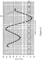
- Figure 6 shows a stress profile 60 which exhibits an asymmetrical profile from one half of the wafer to the other. Without wishing to be limited by any particular theory or conjecture, it is believed that the asymmetry is likely due to small variations in plasma potential through the chamber. A change of 1-2V in potential at the wafer surface can lead to stress differences of the order of 100 MPa. In practice, it is difficult to avoid voltage variations of this order due to small asymmetries in hardware.
- FIG. 7 shows a stepped platen 70 having a puck 72 at the centre of the platen which raises and rotates the wafer between deposition steps. This is a convenient way in which the wafer can be rotated through the deposition process.
- Figure 8 shows a stress profile 80 as a function of wafer radial position obtained using the substrate support shown in Figure 7 .It can be seen that an excellent, almost completely symmetric profile is attained with a relatively small variation (about 90 MPa) in stress across the wafer.
- the invention can be applied to a range of films, including other metal nitrides.
- the invention is particularly applicable to deposition processes where the tolerances tight, especially where it is required that the stress of the deposited film is highly uniform.
Landscapes
- Chemical & Material Sciences (AREA)
- Engineering & Computer Science (AREA)
- Organic Chemistry (AREA)
- Materials Engineering (AREA)
- Mechanical Engineering (AREA)
- Metallurgy (AREA)
- Chemical Kinetics & Catalysis (AREA)
- Physics & Mathematics (AREA)
- Plasma & Fusion (AREA)
- Analytical Chemistry (AREA)
- Physical Vapour Deposition (AREA)
- Electrodes Of Semiconductors (AREA)
- Physical Deposition Of Substances That Are Components Of Semiconductor Devices (AREA)
Applications Claiming Priority (1)
| Application Number | Priority Date | Filing Date | Title |
|---|---|---|---|
| GB201606115 | 2016-04-11 |
Publications (2)
| Publication Number | Publication Date |
|---|---|
| EP3232463A1 EP3232463A1 (en) | 2017-10-18 |
| EP3232463B1 true EP3232463B1 (en) | 2020-06-24 |
Family
ID=58489244
Family Applications (1)
| Application Number | Title | Priority Date | Filing Date |
|---|---|---|---|
| EP17164773.8A Active EP3232463B1 (en) | 2016-04-11 | 2017-04-04 | Dc magnetron sputtering |
Country Status (6)
| Country | Link |
|---|---|
| US (2) | US11008651B2 (ko) |
| EP (1) | EP3232463B1 (ko) |
| JP (1) | JP6948140B2 (ko) |
| KR (1) | KR102353256B1 (ko) |
| CN (2) | CN117568770A (ko) |
| TW (1) | TWI755387B (ko) |
Families Citing this family (10)
| Publication number | Priority date | Publication date | Assignee | Title |
|---|---|---|---|---|
| CN111349899B (zh) * | 2018-12-20 | 2022-02-25 | 上海陛通半导体能源科技股份有限公司 | 物理气相沉积材料的方法和设备 |
| US11384423B2 (en) | 2018-12-26 | 2022-07-12 | Ulvac, Inc. | Sputtering apparatus and sputtering method |
| GB201909538D0 (en) * | 2019-07-02 | 2019-08-14 | Spts Technologies Ltd | Deposition apparatus |
| CN110643962A (zh) * | 2019-09-20 | 2020-01-03 | 深圳市晶相技术有限公司 | 一种半导体设备 |
| CN110643961B (zh) * | 2019-09-20 | 2024-02-06 | 深圳市晶相技术有限公司 | 一种半导体设备的使用方法 |
| KR102778496B1 (ko) * | 2019-10-25 | 2025-03-06 | 어플라이드 머티어리얼스, 인코포레이티드 | 고품질 pvd 막들을 증착하기 위한 방법 |
| EP4085159A4 (en) * | 2019-12-31 | 2023-09-27 | Applied Materials, Inc. | Method and apparatus for deposition of piezo-electric materials |
| GB202001781D0 (en) | 2020-02-10 | 2020-03-25 | Spts Technologies Ltd | Pe-Cvd apparatus and method |
| KR102430218B1 (ko) * | 2020-10-20 | 2022-08-11 | 한국전자기술연구원 | AlN(질화알루미늄) 박막 증착 방법 |
| CN114774872B (zh) * | 2022-04-29 | 2023-09-08 | 北京北方华创微电子装备有限公司 | 磁控管装置及磁控溅射设备 |
Citations (1)
| Publication number | Priority date | Publication date | Assignee | Title |
|---|---|---|---|---|
| US20140268479A1 (en) * | 2013-03-15 | 2014-09-18 | Applied Materials, Inc. | Substrate support chuck cooling for deposition chamber |
Family Cites Families (18)
| Publication number | Priority date | Publication date | Assignee | Title |
|---|---|---|---|---|
| JPS619571A (ja) | 1984-06-22 | 1986-01-17 | Tanaka Kikinzoku Kogyo Kk | 薄膜製造方法 |
| JPH0211761A (ja) * | 1988-06-28 | 1990-01-16 | Tokuda Seisakusho Ltd | スパッタリング装置 |
| JPH06306599A (ja) * | 1993-04-23 | 1994-11-01 | Toshiba Corp | 半導体素子用製造装置 |
| JP3220619B2 (ja) * | 1995-05-24 | 2001-10-22 | 松下電器産業株式会社 | ガス伝熱プラズマ処理装置 |
| US6524971B1 (en) | 1999-12-17 | 2003-02-25 | Agere Systems, Inc. | Method of deposition of films |
| US6506291B2 (en) * | 2001-06-14 | 2003-01-14 | Applied Materials, Inc. | Substrate support with multilevel heat transfer mechanism |
| US6682603B2 (en) | 2002-05-07 | 2004-01-27 | Applied Materials Inc. | Substrate support with extended radio frequency electrode upper surface |
| US6808607B2 (en) * | 2002-09-25 | 2004-10-26 | Advanced Energy Industries, Inc. | High peak power plasma pulsed supply with arc handling |
| US20040060812A1 (en) | 2002-09-27 | 2004-04-01 | Applied Materials, Inc. | Method for modulating stress in films deposited using a physical vapor deposition (PVD) process |
| US6884718B2 (en) | 2003-03-18 | 2005-04-26 | Micron Technology, Inc. | Semiconductor manufacturing process and apparatus for modifying in-film stress of thin films, and product formed thereby |
| JP4721878B2 (ja) * | 2005-11-22 | 2011-07-13 | キヤノンアネルバ株式会社 | スパッタリング装置 |
| US7838800B2 (en) * | 2006-09-25 | 2010-11-23 | Tokyo Electron Limited | Temperature controlled substrate holder having erosion resistant insulating layer for a substrate processing system |
| US8062487B2 (en) * | 2007-06-25 | 2011-11-22 | United Microelectronics Corp. | Wafer supporting device of a sputtering apparatus |
| US8808513B2 (en) | 2008-03-25 | 2014-08-19 | Oem Group, Inc | Stress adjustment in reactive sputtering |
| JP5870568B2 (ja) * | 2011-05-12 | 2016-03-01 | 東京エレクトロン株式会社 | 成膜装置、プラズマ処理装置、成膜方法及び記憶媒体 |
| US9719166B2 (en) * | 2011-06-21 | 2017-08-01 | Spts Technologies Limited | Method of supporting a workpiece during physical vapour deposition |
| US20150311046A1 (en) * | 2014-04-27 | 2015-10-29 | Avago Technologies General Ip (Singapore) Pte. Ltd. | Fabricating low-defect rare-earth doped piezoelectric layer |
| JP6318869B2 (ja) * | 2014-05-30 | 2018-05-09 | 東京エレクトロン株式会社 | 成膜装置 |
-
2017
- 2017-04-04 US US15/478,283 patent/US11008651B2/en active Active
- 2017-04-04 EP EP17164773.8A patent/EP3232463B1/en active Active
- 2017-04-06 JP JP2017076123A patent/JP6948140B2/ja active Active
- 2017-04-10 CN CN202311604805.2A patent/CN117568770A/zh active Pending
- 2017-04-10 TW TW106111883A patent/TWI755387B/zh active
- 2017-04-10 CN CN201710228703.3A patent/CN107313021A/zh active Pending
- 2017-04-11 KR KR1020170046674A patent/KR102353256B1/ko active Active
-
2021
- 2021-04-27 US US17/241,237 patent/US11718908B2/en active Active
Patent Citations (1)
| Publication number | Priority date | Publication date | Assignee | Title |
|---|---|---|---|---|
| US20140268479A1 (en) * | 2013-03-15 | 2014-09-18 | Applied Materials, Inc. | Substrate support chuck cooling for deposition chamber |
Also Published As
| Publication number | Publication date |
|---|---|
| TW201802863A (zh) | 2018-01-16 |
| CN117568770A (zh) | 2024-02-20 |
| KR20170116587A (ko) | 2017-10-19 |
| TWI755387B (zh) | 2022-02-21 |
| US11718908B2 (en) | 2023-08-08 |
| CN107313021A (zh) | 2017-11-03 |
| US20210246545A1 (en) | 2021-08-12 |
| EP3232463A1 (en) | 2017-10-18 |
| JP2017190526A (ja) | 2017-10-19 |
| US20170294294A1 (en) | 2017-10-12 |
| KR102353256B1 (ko) | 2022-01-18 |
| JP6948140B2 (ja) | 2021-10-13 |
| US11008651B2 (en) | 2021-05-18 |
Similar Documents
| Publication | Publication Date | Title |
|---|---|---|
| EP3232463B1 (en) | Dc magnetron sputtering | |
| US11961722B2 (en) | Method and apparatus for controlling stress variation in a material layer formed via pulsed DC physical vapor deposition | |
| TWI616552B (zh) | 製程工具防護板及具有防護板之物理氣相沉積室 | |
| EP3075876B1 (en) | Method and apparatus for depositing a material | |
| US9928997B2 (en) | Apparatus for PVD dielectric deposition | |
| TWI899147B (zh) | 形成壓電膜之方法以及處理基板之設備 | |
| US20190051768A1 (en) | Method for graded anti-reflective coatings by physical vapor deposition | |
| US6607640B2 (en) | Temperature control of a substrate | |
| TWI754503B (zh) | 用於沉積壓電材料的方法及裝置 | |
| EP2905354B1 (en) | Method of processing a substrate | |
| US20180057929A1 (en) | Method of Depositing Aluminum Oxide Film, Method of Forming the Same, and Sputtering Apparatus | |
| US20250364210A1 (en) | Pecvd trench bottom profile control with pulsed dual rf plasma | |
| US9960023B2 (en) | Methods and apparatus for nodule control in a titanium-tungsten target |
Legal Events
| Date | Code | Title | Description |
|---|---|---|---|
| PUAI | Public reference made under article 153(3) epc to a published international application that has entered the european phase |
Free format text: ORIGINAL CODE: 0009012 |
|
| STAA | Information on the status of an ep patent application or granted ep patent |
Free format text: STATUS: THE APPLICATION HAS BEEN PUBLISHED |
|
| AK | Designated contracting states |
Kind code of ref document: A1 Designated state(s): AL AT BE BG CH CY CZ DE DK EE ES FI FR GB GR HR HU IE IS IT LI LT LU LV MC MK MT NL NO PL PT RO RS SE SI SK SM TR |
|
| AX | Request for extension of the european patent |
Extension state: BA ME |
|
| STAA | Information on the status of an ep patent application or granted ep patent |
Free format text: STATUS: REQUEST FOR EXAMINATION WAS MADE |
|
| 17P | Request for examination filed |
Effective date: 20180418 |
|
| RBV | Designated contracting states (corrected) |
Designated state(s): AL AT BE BG CH CY CZ DE DK EE ES FI FR GB GR HR HU IE IS IT LI LT LU LV MC MK MT NL NO PL PT RO RS SE SI SK SM TR |
|
| STAA | Information on the status of an ep patent application or granted ep patent |
Free format text: STATUS: EXAMINATION IS IN PROGRESS |
|
| 17Q | First examination report despatched |
Effective date: 20190726 |
|
| GRAP | Despatch of communication of intention to grant a patent |
Free format text: ORIGINAL CODE: EPIDOSNIGR1 |
|
| STAA | Information on the status of an ep patent application or granted ep patent |
Free format text: STATUS: GRANT OF PATENT IS INTENDED |
|
| INTG | Intention to grant announced |
Effective date: 20200415 |
|
| GRAS | Grant fee paid |
Free format text: ORIGINAL CODE: EPIDOSNIGR3 |
|
| GRAA | (expected) grant |
Free format text: ORIGINAL CODE: 0009210 |
|
| STAA | Information on the status of an ep patent application or granted ep patent |
Free format text: STATUS: THE PATENT HAS BEEN GRANTED |
|
| AK | Designated contracting states |
Kind code of ref document: B1 Designated state(s): AL AT BE BG CH CY CZ DE DK EE ES FI FR GB GR HR HU IE IS IT LI LT LU LV MC MK MT NL NO PL PT RO RS SE SI SK SM TR |
|
| REG | Reference to a national code |
Ref country code: GB Ref legal event code: FG4D |
|
| REG | Reference to a national code |
Ref country code: CH Ref legal event code: EP |
|
| REG | Reference to a national code |
Ref country code: AT Ref legal event code: REF Ref document number: 1284741 Country of ref document: AT Kind code of ref document: T Effective date: 20200715 |
|
| REG | Reference to a national code |
Ref country code: DE Ref legal event code: R096 Ref document number: 602017018543 Country of ref document: DE |
|
| REG | Reference to a national code |
Ref country code: IE Ref legal event code: FG4D |
|
| PG25 | Lapsed in a contracting state [announced via postgrant information from national office to epo] |
Ref country code: SE Free format text: LAPSE BECAUSE OF FAILURE TO SUBMIT A TRANSLATION OF THE DESCRIPTION OR TO PAY THE FEE WITHIN THE PRESCRIBED TIME-LIMIT Effective date: 20200624 Ref country code: FI Free format text: LAPSE BECAUSE OF FAILURE TO SUBMIT A TRANSLATION OF THE DESCRIPTION OR TO PAY THE FEE WITHIN THE PRESCRIBED TIME-LIMIT Effective date: 20200624 Ref country code: GR Free format text: LAPSE BECAUSE OF FAILURE TO SUBMIT A TRANSLATION OF THE DESCRIPTION OR TO PAY THE FEE WITHIN THE PRESCRIBED TIME-LIMIT Effective date: 20200925 Ref country code: NO Free format text: LAPSE BECAUSE OF FAILURE TO SUBMIT A TRANSLATION OF THE DESCRIPTION OR TO PAY THE FEE WITHIN THE PRESCRIBED TIME-LIMIT Effective date: 20200924 Ref country code: LT Free format text: LAPSE BECAUSE OF FAILURE TO SUBMIT A TRANSLATION OF THE DESCRIPTION OR TO PAY THE FEE WITHIN THE PRESCRIBED TIME-LIMIT Effective date: 20200624 |
|
| REG | Reference to a national code |
Ref country code: LT Ref legal event code: MG4D |
|
| PG25 | Lapsed in a contracting state [announced via postgrant information from national office to epo] |
Ref country code: LV Free format text: LAPSE BECAUSE OF FAILURE TO SUBMIT A TRANSLATION OF THE DESCRIPTION OR TO PAY THE FEE WITHIN THE PRESCRIBED TIME-LIMIT Effective date: 20200624 Ref country code: RS Free format text: LAPSE BECAUSE OF FAILURE TO SUBMIT A TRANSLATION OF THE DESCRIPTION OR TO PAY THE FEE WITHIN THE PRESCRIBED TIME-LIMIT Effective date: 20200624 Ref country code: BG Free format text: LAPSE BECAUSE OF FAILURE TO SUBMIT A TRANSLATION OF THE DESCRIPTION OR TO PAY THE FEE WITHIN THE PRESCRIBED TIME-LIMIT Effective date: 20200924 Ref country code: HR Free format text: LAPSE BECAUSE OF FAILURE TO SUBMIT A TRANSLATION OF THE DESCRIPTION OR TO PAY THE FEE WITHIN THE PRESCRIBED TIME-LIMIT Effective date: 20200624 |
|
| REG | Reference to a national code |
Ref country code: NL Ref legal event code: MP Effective date: 20200624 |
|
| REG | Reference to a national code |
Ref country code: AT Ref legal event code: MK05 Ref document number: 1284741 Country of ref document: AT Kind code of ref document: T Effective date: 20200624 |
|
| PG25 | Lapsed in a contracting state [announced via postgrant information from national office to epo] |
Ref country code: NL Free format text: LAPSE BECAUSE OF FAILURE TO SUBMIT A TRANSLATION OF THE DESCRIPTION OR TO PAY THE FEE WITHIN THE PRESCRIBED TIME-LIMIT Effective date: 20200624 Ref country code: AL Free format text: LAPSE BECAUSE OF FAILURE TO SUBMIT A TRANSLATION OF THE DESCRIPTION OR TO PAY THE FEE WITHIN THE PRESCRIBED TIME-LIMIT Effective date: 20200624 |
|
| PG25 | Lapsed in a contracting state [announced via postgrant information from national office to epo] |
Ref country code: RO Free format text: LAPSE BECAUSE OF FAILURE TO SUBMIT A TRANSLATION OF THE DESCRIPTION OR TO PAY THE FEE WITHIN THE PRESCRIBED TIME-LIMIT Effective date: 20200624 Ref country code: IT Free format text: LAPSE BECAUSE OF FAILURE TO SUBMIT A TRANSLATION OF THE DESCRIPTION OR TO PAY THE FEE WITHIN THE PRESCRIBED TIME-LIMIT Effective date: 20200624 Ref country code: CZ Free format text: LAPSE BECAUSE OF FAILURE TO SUBMIT A TRANSLATION OF THE DESCRIPTION OR TO PAY THE FEE WITHIN THE PRESCRIBED TIME-LIMIT Effective date: 20200624 Ref country code: SM Free format text: LAPSE BECAUSE OF FAILURE TO SUBMIT A TRANSLATION OF THE DESCRIPTION OR TO PAY THE FEE WITHIN THE PRESCRIBED TIME-LIMIT Effective date: 20200624 Ref country code: EE Free format text: LAPSE BECAUSE OF FAILURE TO SUBMIT A TRANSLATION OF THE DESCRIPTION OR TO PAY THE FEE WITHIN THE PRESCRIBED TIME-LIMIT Effective date: 20200624 Ref country code: AT Free format text: LAPSE BECAUSE OF FAILURE TO SUBMIT A TRANSLATION OF THE DESCRIPTION OR TO PAY THE FEE WITHIN THE PRESCRIBED TIME-LIMIT Effective date: 20200624 Ref country code: PT Free format text: LAPSE BECAUSE OF FAILURE TO SUBMIT A TRANSLATION OF THE DESCRIPTION OR TO PAY THE FEE WITHIN THE PRESCRIBED TIME-LIMIT Effective date: 20201026 Ref country code: ES Free format text: LAPSE BECAUSE OF FAILURE TO SUBMIT A TRANSLATION OF THE DESCRIPTION OR TO PAY THE FEE WITHIN THE PRESCRIBED TIME-LIMIT Effective date: 20200624 |
|
| PG25 | Lapsed in a contracting state [announced via postgrant information from national office to epo] |
Ref country code: SK Free format text: LAPSE BECAUSE OF FAILURE TO SUBMIT A TRANSLATION OF THE DESCRIPTION OR TO PAY THE FEE WITHIN THE PRESCRIBED TIME-LIMIT Effective date: 20200624 Ref country code: PL Free format text: LAPSE BECAUSE OF FAILURE TO SUBMIT A TRANSLATION OF THE DESCRIPTION OR TO PAY THE FEE WITHIN THE PRESCRIBED TIME-LIMIT Effective date: 20200624 Ref country code: IS Free format text: LAPSE BECAUSE OF FAILURE TO SUBMIT A TRANSLATION OF THE DESCRIPTION OR TO PAY THE FEE WITHIN THE PRESCRIBED TIME-LIMIT Effective date: 20201024 |
|
| REG | Reference to a national code |
Ref country code: DE Ref legal event code: R097 Ref document number: 602017018543 Country of ref document: DE |
|
| PG25 | Lapsed in a contracting state [announced via postgrant information from national office to epo] |
Ref country code: DK Free format text: LAPSE BECAUSE OF FAILURE TO SUBMIT A TRANSLATION OF THE DESCRIPTION OR TO PAY THE FEE WITHIN THE PRESCRIBED TIME-LIMIT Effective date: 20200624 |
|
| PLBE | No opposition filed within time limit |
Free format text: ORIGINAL CODE: 0009261 |
|
| STAA | Information on the status of an ep patent application or granted ep patent |
Free format text: STATUS: NO OPPOSITION FILED WITHIN TIME LIMIT |
|
| 26N | No opposition filed |
Effective date: 20210325 |
|
| PG25 | Lapsed in a contracting state [announced via postgrant information from national office to epo] |
Ref country code: SI Free format text: LAPSE BECAUSE OF FAILURE TO SUBMIT A TRANSLATION OF THE DESCRIPTION OR TO PAY THE FEE WITHIN THE PRESCRIBED TIME-LIMIT Effective date: 20200624 |
|
| PG25 | Lapsed in a contracting state [announced via postgrant information from national office to epo] |
Ref country code: MC Free format text: LAPSE BECAUSE OF FAILURE TO SUBMIT A TRANSLATION OF THE DESCRIPTION OR TO PAY THE FEE WITHIN THE PRESCRIBED TIME-LIMIT Effective date: 20200624 |
|
| GBPC | Gb: european patent ceased through non-payment of renewal fee |
Effective date: 20210404 |
|
| PG25 | Lapsed in a contracting state [announced via postgrant information from national office to epo] |
Ref country code: LU Free format text: LAPSE BECAUSE OF NON-PAYMENT OF DUE FEES Effective date: 20210404 |
|
| REG | Reference to a national code |
Ref country code: BE Ref legal event code: MM Effective date: 20210430 |
|
| PG25 | Lapsed in a contracting state [announced via postgrant information from national office to epo] |
Ref country code: GB Free format text: LAPSE BECAUSE OF NON-PAYMENT OF DUE FEES Effective date: 20210404 Ref country code: CH Free format text: LAPSE BECAUSE OF NON-PAYMENT OF DUE FEES Effective date: 20210430 Ref country code: LI Free format text: LAPSE BECAUSE OF NON-PAYMENT OF DUE FEES Effective date: 20210430 |
|
| PG25 | Lapsed in a contracting state [announced via postgrant information from national office to epo] |
Ref country code: IE Free format text: LAPSE BECAUSE OF NON-PAYMENT OF DUE FEES Effective date: 20210404 |
|
| PG25 | Lapsed in a contracting state [announced via postgrant information from national office to epo] |
Ref country code: IS Free format text: LAPSE BECAUSE OF FAILURE TO SUBMIT A TRANSLATION OF THE DESCRIPTION OR TO PAY THE FEE WITHIN THE PRESCRIBED TIME-LIMIT Effective date: 20201024 |
|
| PG25 | Lapsed in a contracting state [announced via postgrant information from national office to epo] |
Ref country code: BE Free format text: LAPSE BECAUSE OF NON-PAYMENT OF DUE FEES Effective date: 20210430 |
|
| PG25 | Lapsed in a contracting state [announced via postgrant information from national office to epo] |
Ref country code: HU Free format text: LAPSE BECAUSE OF FAILURE TO SUBMIT A TRANSLATION OF THE DESCRIPTION OR TO PAY THE FEE WITHIN THE PRESCRIBED TIME-LIMIT; INVALID AB INITIO Effective date: 20170404 |
|
| PG25 | Lapsed in a contracting state [announced via postgrant information from national office to epo] |
Ref country code: CY Free format text: LAPSE BECAUSE OF FAILURE TO SUBMIT A TRANSLATION OF THE DESCRIPTION OR TO PAY THE FEE WITHIN THE PRESCRIBED TIME-LIMIT Effective date: 20200624 |
|
| P01 | Opt-out of the competence of the unified patent court (upc) registered |
Effective date: 20230525 |
|
| REG | Reference to a national code |
Ref country code: DE Ref legal event code: R082 Ref document number: 602017018543 Country of ref document: DE Representative=s name: KANDLBINDER, MARKUS, DIPL.-PHYS., DE |
|
| PG25 | Lapsed in a contracting state [announced via postgrant information from national office to epo] |
Ref country code: MK Free format text: LAPSE BECAUSE OF FAILURE TO SUBMIT A TRANSLATION OF THE DESCRIPTION OR TO PAY THE FEE WITHIN THE PRESCRIBED TIME-LIMIT Effective date: 20200624 |
|
| PG25 | Lapsed in a contracting state [announced via postgrant information from national office to epo] |
Ref country code: MT Free format text: LAPSE BECAUSE OF FAILURE TO SUBMIT A TRANSLATION OF THE DESCRIPTION OR TO PAY THE FEE WITHIN THE PRESCRIBED TIME-LIMIT Effective date: 20200624 |
|
| PGFP | Annual fee paid to national office [announced via postgrant information from national office to epo] |
Ref country code: DE Payment date: 20250429 Year of fee payment: 9 |
|
| PGFP | Annual fee paid to national office [announced via postgrant information from national office to epo] |
Ref country code: FR Payment date: 20250425 Year of fee payment: 9 |
|
| PG25 | Lapsed in a contracting state [announced via postgrant information from national office to epo] |
Ref country code: TR Free format text: LAPSE BECAUSE OF FAILURE TO SUBMIT A TRANSLATION OF THE DESCRIPTION OR TO PAY THE FEE WITHIN THE PRESCRIBED TIME-LIMIT Effective date: 20200624 |