EP3236309B1 - Anzeigevorrichtung - Google Patents
Anzeigevorrichtung Download PDFInfo
- Publication number
- EP3236309B1 EP3236309B1 EP17154020.6A EP17154020A EP3236309B1 EP 3236309 B1 EP3236309 B1 EP 3236309B1 EP 17154020 A EP17154020 A EP 17154020A EP 3236309 B1 EP3236309 B1 EP 3236309B1
- Authority
- EP
- European Patent Office
- Prior art keywords
- lines
- sub
- insulating layer
- pads
- display device
- Prior art date
- Legal status (The legal status is an assumption and is not a legal conclusion. Google has not performed a legal analysis and makes no representation as to the accuracy of the status listed.)
- Active
Links
Images







Classifications
-
- G—PHYSICS
- G02—OPTICS
- G02F—OPTICAL DEVICES OR ARRANGEMENTS FOR THE CONTROL OF LIGHT BY MODIFICATION OF THE OPTICAL PROPERTIES OF THE MEDIA OF THE ELEMENTS INVOLVED THEREIN; NON-LINEAR OPTICS; FREQUENCY-CHANGING OF LIGHT; OPTICAL LOGIC ELEMENTS; OPTICAL ANALOGUE/DIGITAL CONVERTERS
- G02F1/00—Devices or arrangements for the control of the intensity, colour, phase, polarisation or direction of light arriving from an independent light source, e.g. switching, gating or modulating; Non-linear optics
- G02F1/01—Devices or arrangements for the control of the intensity, colour, phase, polarisation or direction of light arriving from an independent light source, e.g. switching, gating or modulating; Non-linear optics for the control of the intensity, phase, polarisation or colour
- G02F1/13—Devices or arrangements for the control of the intensity, colour, phase, polarisation or direction of light arriving from an independent light source, e.g. switching, gating or modulating; Non-linear optics for the control of the intensity, phase, polarisation or colour based on liquid crystals, e.g. single liquid crystal display cells
- G02F1/133—Constructional arrangements; Operation of liquid crystal cells; Circuit arrangements
- G02F1/1333—Constructional arrangements; Manufacturing methods
- G02F1/1345—Conductors connecting electrodes to cell terminals
-
- H—ELECTRICITY
- H10—SEMICONDUCTOR DEVICES; ELECTRIC SOLID-STATE DEVICES NOT OTHERWISE PROVIDED FOR
- H10D—INORGANIC ELECTRIC SEMICONDUCTOR DEVICES
- H10D86/00—Integrated devices formed in or on insulating or conducting substrates, e.g. formed in silicon-on-insulator [SOI] substrates or on stainless steel or glass substrates
- H10D86/40—Integrated devices formed in or on insulating or conducting substrates, e.g. formed in silicon-on-insulator [SOI] substrates or on stainless steel or glass substrates characterised by multiple TFTs
- H10D86/441—Interconnections, e.g. scanning lines
- H10D86/443—Interconnections, e.g. scanning lines adapted for preventing breakage, peeling or short circuiting
-
- G—PHYSICS
- G02—OPTICS
- G02F—OPTICAL DEVICES OR ARRANGEMENTS FOR THE CONTROL OF LIGHT BY MODIFICATION OF THE OPTICAL PROPERTIES OF THE MEDIA OF THE ELEMENTS INVOLVED THEREIN; NON-LINEAR OPTICS; FREQUENCY-CHANGING OF LIGHT; OPTICAL LOGIC ELEMENTS; OPTICAL ANALOGUE/DIGITAL CONVERTERS
- G02F1/00—Devices or arrangements for the control of the intensity, colour, phase, polarisation or direction of light arriving from an independent light source, e.g. switching, gating or modulating; Non-linear optics
- G02F1/01—Devices or arrangements for the control of the intensity, colour, phase, polarisation or direction of light arriving from an independent light source, e.g. switching, gating or modulating; Non-linear optics for the control of the intensity, phase, polarisation or colour
- G02F1/13—Devices or arrangements for the control of the intensity, colour, phase, polarisation or direction of light arriving from an independent light source, e.g. switching, gating or modulating; Non-linear optics for the control of the intensity, phase, polarisation or colour based on liquid crystals, e.g. single liquid crystal display cells
- G02F1/133—Constructional arrangements; Operation of liquid crystal cells; Circuit arrangements
- G02F1/1333—Constructional arrangements; Manufacturing methods
- G02F1/133305—Flexible substrates, e.g. plastics, organic film
-
- G—PHYSICS
- G02—OPTICS
- G02F—OPTICAL DEVICES OR ARRANGEMENTS FOR THE CONTROL OF LIGHT BY MODIFICATION OF THE OPTICAL PROPERTIES OF THE MEDIA OF THE ELEMENTS INVOLVED THEREIN; NON-LINEAR OPTICS; FREQUENCY-CHANGING OF LIGHT; OPTICAL LOGIC ELEMENTS; OPTICAL ANALOGUE/DIGITAL CONVERTERS
- G02F1/00—Devices or arrangements for the control of the intensity, colour, phase, polarisation or direction of light arriving from an independent light source, e.g. switching, gating or modulating; Non-linear optics
- G02F1/01—Devices or arrangements for the control of the intensity, colour, phase, polarisation or direction of light arriving from an independent light source, e.g. switching, gating or modulating; Non-linear optics for the control of the intensity, phase, polarisation or colour
- G02F1/13—Devices or arrangements for the control of the intensity, colour, phase, polarisation or direction of light arriving from an independent light source, e.g. switching, gating or modulating; Non-linear optics for the control of the intensity, phase, polarisation or colour based on liquid crystals, e.g. single liquid crystal display cells
- G02F1/133—Constructional arrangements; Operation of liquid crystal cells; Circuit arrangements
- G02F1/1333—Constructional arrangements; Manufacturing methods
- G02F1/1345—Conductors connecting electrodes to cell terminals
- G02F1/13458—Terminal pads
-
- G—PHYSICS
- G02—OPTICS
- G02F—OPTICAL DEVICES OR ARRANGEMENTS FOR THE CONTROL OF LIGHT BY MODIFICATION OF THE OPTICAL PROPERTIES OF THE MEDIA OF THE ELEMENTS INVOLVED THEREIN; NON-LINEAR OPTICS; FREQUENCY-CHANGING OF LIGHT; OPTICAL LOGIC ELEMENTS; OPTICAL ANALOGUE/DIGITAL CONVERTERS
- G02F1/00—Devices or arrangements for the control of the intensity, colour, phase, polarisation or direction of light arriving from an independent light source, e.g. switching, gating or modulating; Non-linear optics
- G02F1/01—Devices or arrangements for the control of the intensity, colour, phase, polarisation or direction of light arriving from an independent light source, e.g. switching, gating or modulating; Non-linear optics for the control of the intensity, phase, polarisation or colour
- G02F1/13—Devices or arrangements for the control of the intensity, colour, phase, polarisation or direction of light arriving from an independent light source, e.g. switching, gating or modulating; Non-linear optics for the control of the intensity, phase, polarisation or colour based on liquid crystals, e.g. single liquid crystal display cells
- G02F1/133—Constructional arrangements; Operation of liquid crystal cells; Circuit arrangements
- G02F1/136—Liquid crystal cells structurally associated with a semi-conducting layer or substrate, e.g. cells forming part of an integrated circuit
- G02F1/1362—Active matrix addressed cells
- G02F1/136286—Wiring, e.g. gate line, drain line
-
- H—ELECTRICITY
- H10—SEMICONDUCTOR DEVICES; ELECTRIC SOLID-STATE DEVICES NOT OTHERWISE PROVIDED FOR
- H10D—INORGANIC ELECTRIC SEMICONDUCTOR DEVICES
- H10D86/00—Integrated devices formed in or on insulating or conducting substrates, e.g. formed in silicon-on-insulator [SOI] substrates or on stainless steel or glass substrates
- H10D86/40—Integrated devices formed in or on insulating or conducting substrates, e.g. formed in silicon-on-insulator [SOI] substrates or on stainless steel or glass substrates characterised by multiple TFTs
- H10D86/411—Integrated devices formed in or on insulating or conducting substrates, e.g. formed in silicon-on-insulator [SOI] substrates or on stainless steel or glass substrates characterised by multiple TFTs characterised by materials, geometry or structure of the substrates
-
- H—ELECTRICITY
- H10—SEMICONDUCTOR DEVICES; ELECTRIC SOLID-STATE DEVICES NOT OTHERWISE PROVIDED FOR
- H10D—INORGANIC ELECTRIC SEMICONDUCTOR DEVICES
- H10D86/00—Integrated devices formed in or on insulating or conducting substrates, e.g. formed in silicon-on-insulator [SOI] substrates or on stainless steel or glass substrates
- H10D86/40—Integrated devices formed in or on insulating or conducting substrates, e.g. formed in silicon-on-insulator [SOI] substrates or on stainless steel or glass substrates characterised by multiple TFTs
- H10D86/421—Integrated devices formed in or on insulating or conducting substrates, e.g. formed in silicon-on-insulator [SOI] substrates or on stainless steel or glass substrates characterised by multiple TFTs having a particular composition, shape or crystalline structure of the active layer
- H10D86/423—Integrated devices formed in or on insulating or conducting substrates, e.g. formed in silicon-on-insulator [SOI] substrates or on stainless steel or glass substrates characterised by multiple TFTs having a particular composition, shape or crystalline structure of the active layer comprising semiconductor materials not belonging to the Group IV, e.g. InGaZnO
-
- H—ELECTRICITY
- H10—SEMICONDUCTOR DEVICES; ELECTRIC SOLID-STATE DEVICES NOT OTHERWISE PROVIDED FOR
- H10D—INORGANIC ELECTRIC SEMICONDUCTOR DEVICES
- H10D86/00—Integrated devices formed in or on insulating or conducting substrates, e.g. formed in silicon-on-insulator [SOI] substrates or on stainless steel or glass substrates
- H10D86/40—Integrated devices formed in or on insulating or conducting substrates, e.g. formed in silicon-on-insulator [SOI] substrates or on stainless steel or glass substrates characterised by multiple TFTs
- H10D86/451—Integrated devices formed in or on insulating or conducting substrates, e.g. formed in silicon-on-insulator [SOI] substrates or on stainless steel or glass substrates characterised by multiple TFTs characterised by the compositions or shapes of the interlayer dielectrics
-
- H—ELECTRICITY
- H10—SEMICONDUCTOR DEVICES; ELECTRIC SOLID-STATE DEVICES NOT OTHERWISE PROVIDED FOR
- H10D—INORGANIC ELECTRIC SEMICONDUCTOR DEVICES
- H10D86/00—Integrated devices formed in or on insulating or conducting substrates, e.g. formed in silicon-on-insulator [SOI] substrates or on stainless steel or glass substrates
- H10D86/40—Integrated devices formed in or on insulating or conducting substrates, e.g. formed in silicon-on-insulator [SOI] substrates or on stainless steel or glass substrates characterised by multiple TFTs
- H10D86/60—Integrated devices formed in or on insulating or conducting substrates, e.g. formed in silicon-on-insulator [SOI] substrates or on stainless steel or glass substrates characterised by multiple TFTs wherein the TFTs are in active matrices
-
- H—ELECTRICITY
- H10—SEMICONDUCTOR DEVICES; ELECTRIC SOLID-STATE DEVICES NOT OTHERWISE PROVIDED FOR
- H10K—ORGANIC ELECTRIC SOLID-STATE DEVICES
- H10K59/00—Integrated devices, or assemblies of multiple devices, comprising at least one organic light-emitting element covered by group H10K50/00
- H10K59/10—OLED displays
- H10K59/12—Active-matrix OLED [AMOLED] displays
- H10K59/131—Interconnections, e.g. wiring lines or terminals
-
- H—ELECTRICITY
- H10—SEMICONDUCTOR DEVICES; ELECTRIC SOLID-STATE DEVICES NOT OTHERWISE PROVIDED FOR
- H10K—ORGANIC ELECTRIC SOLID-STATE DEVICES
- H10K77/00—Constructional details of devices covered by this subclass and not covered by groups H10K10/80, H10K30/80, H10K50/80 or H10K59/80
- H10K77/10—Substrates, e.g. flexible substrates
-
- G—PHYSICS
- G02—OPTICS
- G02F—OPTICAL DEVICES OR ARRANGEMENTS FOR THE CONTROL OF LIGHT BY MODIFICATION OF THE OPTICAL PROPERTIES OF THE MEDIA OF THE ELEMENTS INVOLVED THEREIN; NON-LINEAR OPTICS; FREQUENCY-CHANGING OF LIGHT; OPTICAL LOGIC ELEMENTS; OPTICAL ANALOGUE/DIGITAL CONVERTERS
- G02F1/00—Devices or arrangements for the control of the intensity, colour, phase, polarisation or direction of light arriving from an independent light source, e.g. switching, gating or modulating; Non-linear optics
- G02F1/01—Devices or arrangements for the control of the intensity, colour, phase, polarisation or direction of light arriving from an independent light source, e.g. switching, gating or modulating; Non-linear optics for the control of the intensity, phase, polarisation or colour
- G02F1/13—Devices or arrangements for the control of the intensity, colour, phase, polarisation or direction of light arriving from an independent light source, e.g. switching, gating or modulating; Non-linear optics for the control of the intensity, phase, polarisation or colour based on liquid crystals, e.g. single liquid crystal display cells
- G02F1/133—Constructional arrangements; Operation of liquid crystal cells; Circuit arrangements
- G02F1/1333—Constructional arrangements; Manufacturing methods
- G02F1/133345—Insulating layers
-
- G—PHYSICS
- G02—OPTICS
- G02F—OPTICAL DEVICES OR ARRANGEMENTS FOR THE CONTROL OF LIGHT BY MODIFICATION OF THE OPTICAL PROPERTIES OF THE MEDIA OF THE ELEMENTS INVOLVED THEREIN; NON-LINEAR OPTICS; FREQUENCY-CHANGING OF LIGHT; OPTICAL LOGIC ELEMENTS; OPTICAL ANALOGUE/DIGITAL CONVERTERS
- G02F2201/00—Constructional arrangements not provided for in groups G02F1/00 - G02F7/00
- G02F2201/50—Protective arrangements
-
- G—PHYSICS
- G09—EDUCATION; CRYPTOGRAPHY; DISPLAY; ADVERTISING; SEALS
- G09G—ARRANGEMENTS OR CIRCUITS FOR CONTROL OF INDICATING DEVICES USING STATIC MEANS TO PRESENT VARIABLE INFORMATION
- G09G2300/00—Aspects of the constitution of display devices
- G09G2300/04—Structural and physical details of display devices
- G09G2300/0421—Structural details of the set of electrodes
- G09G2300/0426—Layout of electrodes and connections
-
- H—ELECTRICITY
- H05—ELECTRIC TECHNIQUES NOT OTHERWISE PROVIDED FOR
- H05B—ELECTRIC HEATING; ELECTRIC LIGHT SOURCES NOT OTHERWISE PROVIDED FOR; CIRCUIT ARRANGEMENTS FOR ELECTRIC LIGHT SOURCES, IN GENERAL
- H05B45/00—Circuit arrangements for operating light-emitting diodes [LED]
- H05B45/60—Circuit arrangements for operating LEDs comprising organic material, e.g. for operating organic light-emitting diodes [OLED] or polymer light-emitting diodes [PLED]
-
- H—ELECTRICITY
- H10—SEMICONDUCTOR DEVICES; ELECTRIC SOLID-STATE DEVICES NOT OTHERWISE PROVIDED FOR
- H10K—ORGANIC ELECTRIC SOLID-STATE DEVICES
- H10K2102/00—Constructional details relating to the organic devices covered by this subclass
- H10K2102/301—Details of OLEDs
- H10K2102/311—Flexible OLED
-
- H—ELECTRICITY
- H10—SEMICONDUCTOR DEVICES; ELECTRIC SOLID-STATE DEVICES NOT OTHERWISE PROVIDED FOR
- H10K—ORGANIC ELECTRIC SOLID-STATE DEVICES
- H10K2102/00—Constructional details relating to the organic devices covered by this subclass
- H10K2102/301—Details of OLEDs
- H10K2102/341—Short-circuit prevention
-
- H—ELECTRICITY
- H10—SEMICONDUCTOR DEVICES; ELECTRIC SOLID-STATE DEVICES NOT OTHERWISE PROVIDED FOR
- H10K—ORGANIC ELECTRIC SOLID-STATE DEVICES
- H10K59/00—Integrated devices, or assemblies of multiple devices, comprising at least one organic light-emitting element covered by group H10K50/00
- H10K59/10—OLED displays
- H10K59/12—Active-matrix OLED [AMOLED] displays
- H10K59/124—Insulating layers formed between TFT elements and OLED elements
-
- H—ELECTRICITY
- H10—SEMICONDUCTOR DEVICES; ELECTRIC SOLID-STATE DEVICES NOT OTHERWISE PROVIDED FOR
- H10K—ORGANIC ELECTRIC SOLID-STATE DEVICES
- H10K59/00—Integrated devices, or assemblies of multiple devices, comprising at least one organic light-emitting element covered by group H10K50/00
- H10K59/80—Constructional details
- H10K59/87—Passivation; Containers; Encapsulations
- H10K59/873—Encapsulations
- H10K59/8731—Encapsulations multilayered coatings having a repetitive structure, e.g. having multiple organic-inorganic bilayers
-
- H—ELECTRICITY
- H10—SEMICONDUCTOR DEVICES; ELECTRIC SOLID-STATE DEVICES NOT OTHERWISE PROVIDED FOR
- H10K—ORGANIC ELECTRIC SOLID-STATE DEVICES
- H10K77/00—Constructional details of devices covered by this subclass and not covered by groups H10K10/80, H10K30/80, H10K50/80 or H10K59/80
- H10K77/10—Substrates, e.g. flexible substrates
- H10K77/111—Flexible substrates
-
- H—ELECTRICITY
- H10—SEMICONDUCTOR DEVICES; ELECTRIC SOLID-STATE DEVICES NOT OTHERWISE PROVIDED FOR
- H10W—GENERIC PACKAGES, INTERCONNECTIONS, CONNECTORS OR OTHER CONSTRUCTIONAL DETAILS OF DEVICES COVERED BY CLASS H10
- H10W20/00—Interconnections in chips, wafers or substrates
- H10W20/01—Manufacture or treatment
- H10W20/031—Manufacture or treatment of conductive parts of the interconnections
- H10W20/0698—Local interconnections
-
- Y—GENERAL TAGGING OF NEW TECHNOLOGICAL DEVELOPMENTS; GENERAL TAGGING OF CROSS-SECTIONAL TECHNOLOGIES SPANNING OVER SEVERAL SECTIONS OF THE IPC; TECHNICAL SUBJECTS COVERED BY FORMER USPC CROSS-REFERENCE ART COLLECTIONS [XRACs] AND DIGESTS
- Y02—TECHNOLOGIES OR APPLICATIONS FOR MITIGATION OR ADAPTATION AGAINST CLIMATE CHANGE
- Y02E—REDUCTION OF GREENHOUSE GAS [GHG] EMISSIONS, RELATED TO ENERGY GENERATION, TRANSMISSION OR DISTRIBUTION
- Y02E10/00—Energy generation through renewable energy sources
- Y02E10/50—Photovoltaic [PV] energy
- Y02E10/549—Organic PV cells
Definitions
- Embodiments of the inventive concept relate to a display device capable of preventing shorts between lines.
- a display device generally includes a display unit positioned on a substrate. Visibility from various angles may be improved and/or the area of a non-display area may be reduced by bending at least a portion of the display device.
- background art includes: EP2816604 , US2014361262 , and US2008180627 , as well as EP2814074 .
- EP2816604 describes an array substrate including a substrate, a buffer layer disposed on the substrate, a first insulating layer disposed on the buffer layer, a second insulating layer disposed on the first insulating layera plurality of wiring patterns disposed on the second insulating layer, and wherein the wiring patterns are separated from each other and a recess pattern disposed adjacent to the wiring patterns.
- US2014361262 describes a flexible display device including a substrate, a plurality of first pixels, and a plurality of second pixels.
- the substrate includes a foldable bending region and a non-foldable non-bending region.
- Each first pixel is disposed on the bending region.
- Each first pixel is spaced apart from an adjacent first pixel by a first distance.
- Each second pixel is disposed on the non-bending region.
- Each second pixel is spaced apart from an adjacent second pixel by a second distance. The first distance is greater than the second distance.
- US2008180627 describes a mounting terminal substrate including a substrate, mounting terminals arranged in staggered rows on the substrate, each mounting terminals includes a lower conductive film and an upper conductive film, lines that are provided between the mounting terminals in a direction of a row, an insulation film that covers the lines, and opening sections on the respective mounting terminals from which the insulation films are removed.
- a width of the upper conductive film in the direction of the row is greater than a width of the lower conductive film in the direction of the row so as to cover the lower conductive films exposed through the opening sections and is equal to or smaller than a width of the opening section in the direction of the row.
- EP2814074 discloses a flexible display device (100) to reduce a width of a bezel.
- the flexible display device (100) includes a substrate (101) being formed of a flexible material, a plurality of gate lines (GL) and a plurality of data lines (DL) crossing each other, a plurality of pads (PD) formed in a pad area (PDA) of a non-display area (NA), a plurality of links (LK) formed in a link area (LKA) of the non-display area (NA), a plurality of insulation films (102-105) formed over the entire surface of the substrate (101), and a first bending hole (BH1) formed in a bending area (BA) of the non-display area (NA), the first bending hole (BH1) passing through at least one of the insulation films disposed under the link (LK), wherein the bending area (BA) is bent such that the pads (PD) are disposed on the lower surface of the substrate (101).
- a substrate (101) being formed of a flexible material,
- Embodiments of the inventive concept may minimize defects, such as disconnections or shorts, that occur during the manufacturing process for a display device, and may ensure a long life for the display device.
- FIG. 1 is a plan view of a display device according to an embodiment of the inventive concept and FIG. 2 is a perspective view of a display device of FIG. 1 .
- a display device may include a substrate SUB (as shown in FIG. 3 ), a plurality of pixels PXL provided on the substrate SUB, and a line part LP connected to the pixels PXL.
- the substrate SUB may include a display area DA and a non-display area NDA provided on at least one side of the display area DA.
- the substrate SUB may roughly have a rectangular shape. According to an embodiment of the inventive concept, the substrate SUB may include a pair of short sides parallel with each other in a first direction DR1 and a pair of long sides parallel with each other in a second direction DR2.
- the shape of the substrate SUB may be not limited thereto, and may have various shapes.
- the substrate SUB may be provided in a variety of shapes, such as a polygon in a closed form with sides formed by straight lines, a circle with sides formed by a curve, an ellipse, a semicircle including sides formed by a straight line and a curve, a semi elliptical shape, etc.
- the corners of the substrate SUB may be curved.
- portions where adjacent sides meet may be formed by a curve with a predetermined curvature.
- the curvature may be determined differently depending on the location. For example, the curvature may vary depending on where the curve starts and the length of the curve.
- the display area DA may be provided in a shape corresponding to the shape of the substrate SUB, as described above.
- the corners may be formed by a curve.
- the pixels PXL may be provided on or in the display area DA of the substrate SUB to display an image.
- the plurality of pixels PXL may be provided as a minimum unit for displaying the image.
- the pixels PXL may emit light in red, green, or blue, but are not limited thereto.
- the pixels PXL may emit light in cyan, magenta, or yellow.
- the pixels PXL may be an organic light emitting device including an organic layer, but are not limited thereto.
- the pixels PXL may be implemented in various forms, such as a liquid crystal device, an electrophoretic device, or an electrowetting device.
- the plurality of pixels PXL may be arranged in a matrix formation with rows extending in the first direction DR1 and columns extending in the second direction DR2.
- the arrangement of the pixels PXL is not limited thereto, and the pixels PXL may be arranged in a variety of ways.
- the pixels PXL may be arranged in a row direction or in an oblique direction with respect to the first direction DR1 or the second direction DR2.
- the non-display area NDA may be an area in which the pixels PXL are not provided and thus, the image is not displayed.
- the non-display area NDA may include the line part LP connected to the pixels PXL and a driver connected to the pixels PXL that drives the pixels PXL.
- the line part LP may be connected to the pixels PXL.
- the line part LP may provide a signal to each of the pixels PXL.
- the line part LP may include a scan line, a data line, and a driving voltage line, and may further includes other lines as needed.
- the line part LP may be provided over the display area DA and the non-display area NDA.
- the line part LP may be connected to the driver.
- the driver may provide a signal to each of the pixels PXL through the line part LP and control the driving of each of the pixels PXL.
- the driver may include a scan driver that provides a scan signal to each of the pixels PXL through the scan line, a data driver that provides a data signal to each of the pixels PXL through the data line, and a timing controller that controls the scan driver and the data driver.
- the scan driver may be directly mounted on the substrate SUB.
- the scan driver may be formed when the pixels PXL are formed.
- the inventive concept is not limited thereto.
- the scan driver may be formed on a separate chip and provided as a chip-on-glass type on the substrate SUB, or may be mounted on a printing circuit board and connected to the substrate SUB through a connecting member.
- the data driver may be directly mounted on the substrate SUB, but is not limited thereto.
- the data driver may be formed on a separate chip and provided as a chip-on-glass type on the substrate SUB, or mounted on a printing circuit board and connected to the substrate SUB through a connecting member.
- the data driver may be formed in a chip on layer or chip-on-film COF shape and connected to the substrate SUB.
- the non-display area NDA may further include an additional area ADA protruding from a portion thereof.
- the additional area ADA may protrude from the sides of the substrate SUB constituting the non-display area NDA.
- the additional area ADA may protrude from one of the short sides of the substrate SUB, as illustrated in FIG. 1 .
- the additional area ADA may protrude from one of the long sides or from two or more sides.
- the data driver may be provided with or connected to the additional area ADA, but the data driver is not limited thereto and may be provided in various constituent elements.
- the display device has flexibility and the display device is folded or bent at the flexible portion.
- the display device includes a bendable area BA (or foldable area) that has flexibility and can be bent in one direction, and a flat area provided on at least one side of the bendable area BA that is relatively flat (e.g., not bent).
- the flat area may or may not have flexibility.
- the bendable area BA may be provided on the additional area ADA.
- the flat area includes a first flat area FA1 and a second flat area FA2, spaced apart from each other with the bendable area BA disposed therebetween.
- the bendable area BA is spaced apart from the display area DA.
- a line where the display device is folded may be defined as a folding line.
- the folding line may be provided in the bendable area BA.
- the term "bendable” indicates that the structure is not fixed and to "fold” is to change the structure from an original type to a different type.
- one or more specific lines may be folded, curved, or rolled along the folding line.
- the sides of the flat area FA1 and the flat area FA2 nearest to the bendable area BA may be arranged in parallel and opposite to each other, as illustrated in FIG. 1 .
- the inventive concept is not limited thereto.
- these sides of the flat area FA1 and the flat area FA2 may be folded at a predetermined angle (e.g., an acute angle, a right angle, or an obtuse angle) with the bendable area BA disposed therebetween.
- the additional area ADA may be bent along the folding line, such that a width of a bezel may be reduced.
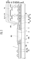
- FIG. 3 is a cross sectional view taken along line I-I' of FIG. 1 according to an embodiment of the inventive concept.
- the display device may have a partially bent shape as shown in FIG. 2 .
- FIG. 3 for convenience of explanation, a display device that is not bent is illustrated.
- the display device is configured to be bent and is illustrated in its form prior to bending.
- a display device prior to bending is illustrated in the cross sectional or plan views of the embodiments described below as well.
- the display area DA is provided with the plurality of pixels PXL.
- Each of the pixels PXL may include a transistor connected to a corresponding line in the line part LP, an organic light emitting device connected to the transistor, and a capacitor Cst.
- the transistor may include a driving transistor for controlling the organic light emitting device and a switching transistor for switching the driving transistor.
- the pixels PXL may be implemented with a stacked layer structure as shown in FIG. 3 .
- a single pixel PXL is illustrated with a single transistor and a single capacitor for convenience of explanation, but the inventive concept is not limited thereto.
- two or more transistors and one or more capacitors may be included in the single pixel PXL, or three or more transistors and two or more capacitors may be included in the single pixel PXL.
- the pixels PXL may be provided on the substrate SUB.
- the substrate SUB may be made of an insulating material such as glass or resin.
- the substrate SUB is made of a material having the flexibility to be bent or folded, and may have a single layer structure or a multilayer structure.
- the substrate SUB may include one of polystyrene, polyvinyl alcohol, polymethyl methacrylate, polyethersulfone, polyacrylate, polyetherimide, polyethylene naphthalate, polyethylene terephthalate, polyphenylene sulfide, polyarylate, polyimide, polycarbonate, cellulose triacetate, or cellulose acetate propionate.
- the material constituting the substrate SUB may be varied and may include fiber reinforced plastic (FRP) or the like.
- a buffer layer BF is formed on the substrate SUB.
- the buffer layer BF prevents diffusion of impurities to the switching transistors and the driving transistors.
- the buffer layer BF may be an inorganic insulating layer made of an inorganic material.
- the buffer layer BF may be formed of silicon nitride, silicon oxide, silicon oxynitride, etc.
- the buffer layer BF may be omitted depending on the material and process conditions of the substrate SUB.
- the active pattern ACT is provided on the buffer layer BF.
- the active pattern ACT may be formed of a semiconductor material.
- the active pattern ACT may include a source area, a drain area, and a channel area provided between the source area and the drain area.
- the active pattern ACT may be a semiconductor pattern formed of polysilicon, amorphous silicon, and an oxide semiconductor.
- the channel area may be an intrinsic semiconductor having a semiconductor pattern that is not doped with the impurities.
- the source area and the drain area may have a semiconductor pattern that is doped with the impurities.
- the impurities may be n-type impurity, p-type impurity, or other metals.
- a gate insulating layer GI is provided on the active pattern ACT.
- the gate insulating layer GI may be an inorganic insulating layer made of an inorganic material.
- the inorganic material may be used as an inorganic insulating material, such as polysiloxane, silicon nitride, silicon oxide, or silicon oxynitride.
- a gate electrode GE and a capacitor lower electrode LE are provided on the gate insulating layer GI.
- the gate electrode GE may be formed to cover an area corresponding to the channel area of the active pattern ACT.
- the gate electrode GE and the capacitor lower electrode LE may be made of metal.
- the gate electrode GE may be made of at least one of gold (Au), silver (Ag), aluminum (Al), molybdenum (Mo), chromium (Cr), titanium (Ti), nickel (Ni), neodymium (Nd), copper (Cu), or an alloy of metals.
- the gate electrode GE may be formed as a single layer, but is not limited thereto and may be formed with a multilayer structure in which the above-described metals and/or an alloy of two or more metals are formed.
- other lines including scan lines may be provided on the same layer as the gate electrode GE and the capacitor lower electrode LE with substantially the same material. These other lines may be directly or indirectly connected to a portion (e.g., the gate electrode GE) of the transistor in each of the pixels PXL.
- the insulating interlayer IL is provided on the gate electrode GE and the capacitor lower electrode LE.
- the insulating interlayer IL may be an inorganic insulating layer made of an inorganic material.
- the inorganic material may include polysiloxane, silicon nitride, silicon oxide, silicon oxynitride, or the like.
- a capacitor upper electrode UE is provided on the insulating interlayer IL.
- the capacitor upper electrode UE may be made of metal.
- the capacitor upper electrode UE may be formed of at least one gold (Au), silver (Ag), aluminum (Al), molybdenum (Mo), chromium (Cr), titanium (Ti), nickel (Ni), neodymium (Nd), copper (Cu), or an alloy of metals.
- the capacitor upper electrode UE may be formed with a single layer or multilayer structure, similar to the gate electrode GE as described above.
- the capacitor lower electrode LE and the capacitor upper electrode UE constitute a capacitor with the insulating interlayer IL interposed therebetween.
- the capacitor Cst includes the capacitor lower electrode LE and the capacitor upper electrode UE, but the capacitor Cst is not limited thereto and may be implemented in a variety of ways.
- a first insulating layer INS1 is provided on the capacitor upper electrode UE.
- the first insulating layer INS1 may be an inorganic insulating layer made of an inorganic material.
- the inorganic material may include polysiloxane, silicon nitride, silicon oxide, silicon oxynitride, or the like.
- a source electrode SE and a drain electrode DE are provided on the first insulating layer INS1.
- the source electrode SE and the drain electrode DE may contact the source area and the drain area, respectively, through a contact hole formed on the first insulating layer INS1, the insulating interlayer IL, and the gate insulating layer GI.
- the source electrode SE and the drain electrode DE may be made of metal.
- the source electrode SE and the drain electrode DE may be formed of gold (Au), silver (Ag), aluminum (Al), molybdenum (Mo), chromium (Cr), titanium (Ti), nickel (Ni), neodymium (Nd), copper (Cu), or an alloy of metals.
- the source electrode SE and the drain electrode DE may be formed with a single layer or multilayer structure, similar to the gate electrode GE as described above.
- data lines or power lines may be provided on the same layer as the source electrode SE and the drain electrode DE using substantially the same material.
- the data lines or the power lines may be directly or indirectly connected to a portion of the transistors in each of the pixels PXL, for example, the source electrode SE and/or the drain electrode DE.
- a passivation layer PSV is provided on the source electrode SE and the drain electrode DE.
- the passivation layer PSV may be an inorganic insulating layer made of an inorganic material.
- the inorganic material may include polysiloxane, silicon nitride, silicon oxide, silicon oxynitride, or the like.
- a third insulating layer INS3 is provided on the passivation layer PSV.
- the third insulating layer INS3 may be an organic insulating layer made of an organic material.
- the organic material may include an organic insulating material, such as a polyacrylic compound, a polyimide-based compound, a fluorine-containing carbon compound such as Teflon, or a benzocyclobutene compound.
- a connecting pattern CNP is provided on the third insulating layer INS3.
- the connecting pattern CNP may be connected to the drain electrode DE of the transistor via a contact hole passing through the third insulating layer INS3 and the passivation layer PSV.
- the connecting pattern CNP may be formed of at least one metal, for example, gold (Au), silver (Ag), aluminum (Al), molybdenum (Mo), chromium (Cr), titanium (Ti), nickel (Ni), neodymium (Nd), copper (Cu), or an alloy of metals.
- the connecting pattern CNP may be formed with a single layer or multilayer structure, similar to the gate electrode GE described above.
- other lines such as a dummy power line may be provided on the same layer as the connecting pattern CNP with substantially the same material.
- a fourth insulating layer INS4 is provided on the connecting pattern CNP.
- the fourth insulating layer INS4 may be an organic insulating layer made of an organic material.
- the organic material may include an organic insulating material, such as a polyacrylic compound, a polyimide-based compound, a fluorine-containing carbon compound such as Teflon, or a benzocyclobutene compound.
- a first electrode EL1 is provided on the fourth insulating layer INS4.
- the first electrode EL1 is connected to the connecting pattern CNP through a contact hole penetrating the fourth insulating layer INS4, and is connected to the drain electrode DE through the contact hole penetrating the third insulating layer INS3 and the passivation layer PSV.
- the first electrode EL1 may be used as one of an anode or a cathode.
- the passivation layer PSV, the third insulating layer INS3, and the fourth insulating layer INS4 may be provided on the drain electrode DE, but the arrangement of the layers may be changed.
- the passivation layer PSV may be provided on the drain electrode DE, and the first electrode EL1 may be provided on the passivation layer PSV.
- the passivation layer PSV and the third insulating layer INS3 may be provided, and the first electrode EL1 may be provided on the third insulating layer INS3.
- the connecting pattern CNP may be omitted and the first electrode EL1 may be directly connected to the drain electrode DE.
- the first electrode EL1 may be formed of a metal layer using an alloy of Ag, Mg, Al, Pt, Pd, Au, Ni, Nd, Ir, or Cr and/or indium tin oxide (ITO), indium zinc oxide (IZO), zinc oxide (ZnO), or indium tin zinc oxide (ITZO).
- ITO indium tin oxide
- IZO indium zinc oxide
- ZnO zinc oxide
- ITZO indium tin zinc oxide
- the first electrode EL1 is made of a single type of metal, but the first electrode EL1 is not limited thereto and may be made of two or more metals, e.g., an alloy of Ag and Mg.
- the first electrode EL1 may be formed of a transparent conductive layer when providing the image in a lower direction of the substrate SUB.
- the first electrode EL1 may be formed of a metal reflective layer and/or a transparent conductive layer when providing the image in an upper direction of the substrate SUB.
- a pixel defining layer PDL for partitioning an area so as to correspond to each of the pixels PXL is provided on the substrate SUB.
- the pixel defining layer PDL may be an organic insulating layer made of an organic material.
- the organic material may include an organic insulating material, such as a polyacrylic compound, a polyimide-based compound, a fluorine-containing carbon compound such as Teflon, or a benzocyclobutene compound.
- the pixel defining layer PDL exposes an upper surface of the first electrode EL1, and protrudes from the substrate SUB along a periphery of the pixel PXL.
- An organic layer OL is provided in an area surrounded by the pixel defining layer PDL.
- the organic layer OL may include a material with a low molecular weight or a polymer.
- the material with a low molecular weight includes copper phthalocyanine (CuPc), N,N-di(naphthalene-1-yl)-N,N'-diphenylbenzidine (NPB), or tris-8-hydroxyquinoline aluminum (Alq3). These materials may be formed by a vacuum deposition method.
- the polymer material may include PEDOT, poly phenylenevinylene (PPV), polyfluorene, or the like.
- the organic layer OL may be provided as a single layer or may be provided with multiple layers that include a variety of functional layers.
- a hole injection layer HIL, a hole transport layer HTL, an emitting layer EML, an electron transport layer ETL, an electron injection layer EIL, and the like may have a single structure or a composite structure.
- the organic layer OL may be formed by a screen printing method, an inkjet printing method, a laser induced thermal imaging (LITI) method, etc.
- LITI laser induced thermal imaging
- the organic layer OL may not be necessarily limited thereto, and may have a variety of structures. At least a portion of the organic layer OL may be integrally formed over the first electrode EL1, or may be separately provided to correspond to the first electrode EL1.
- a second electrode EL2 is formed on the organic layer OL.
- the second electrode EL2 may be provided for each of the pixels PXL.
- the plurality of second electrodes EL2 may be provided to cover most of the display area DA and shared by the plurality of pixels PXL.
- the second electrode EL2 may be used as one of an anode or a cathode.
- the second electrode EL2 may be used as a cathode, and when the first electrode EL1 is a cathode, the second electrode EL2 may be used as an anode.
- the second electrode EL2 may be formed of a metal layer including Ag, Mg, Al, Pt, Pd, Au, Ni, Nd, Ir, Cr, etc. or a transparent conductive layer including, e.g., indium tin oxide (ITO), indium zinc oxide (IZO), zinc oxide (ZnO), or indium tin zinc oxide (ITZO).
- ITO indium tin oxide
- IZO indium zinc oxide
- ZnO zinc oxide
- ITZO indium tin zinc oxide
- ITZO indium tin zinc oxide
- the second electrode EL2 may be formed with a double layer structure or a multiple layer structure containing a metal thin film.
- the second electrode EL2 may be formed of a triple layer of ITO/Ag/ITO.
- the second electrode EL2 When providing the image in the lower direction of the substrate SUB, the second electrode EL2 may be formed of a metal reflective layer and/or a transparent conductive layer. When providing the image in the upper direction of the substrate SUB, the second electrode EL2 may be formed of a transparent conductive layer.
- a sealing layer SL is provided on the second electrode EL2.
- the sealing layer SL may be made of a single layer or multiple layers.
- the sealing layer SL may be formed of a first sealing layer SL1, a second sealing layer SL2, and a third sealing layer SL3.
- the first sealing layer SL1 to the third sealing layer SL3 may be made of an organic material and/or an inorganic material.
- the third sealing layer SL3 arranged as the outermost sealing layer may be made of an inorganic material.
- the first sealing layer SL1 may be made of an inorganic material
- the second sealing layer SL2 may be made of an organic material
- the third sealing layer SL3 may be made of an inorganic material.
- infiltration of moisture or oxygen may be better prevented, but they are more susceptible to cracks due to less elasticity or flexibility.
- Spreading of cracks may be prevented by forming the first sealing layer SL1 and the third sealing layer SL3 with inorganic material, and forming the second sealing layer SL2 with organic material.
- the second sealing layer SL2 formed with organic material may be completely covered by the third sealing layer SL3 so that the end portions of the second sealing layer SL2 are not externally exposed.
- An organic insulating material may be used for the organic material, such as a polyacrylic compound, a polyimide-based compound, a fluorine-containing carbon compound such as Teflon, and a benzocyclobutene compound.
- Polysiloxane, silicon nitride, silicon oxide, or silicon oxynitride may be used for the inorganic material.
- the organic layer OL which forms a light emitting device, may be easily damaged by moisture or oxygen from external sources.
- the sealing layer SL covers the organic layer OL for protection.
- the sealing layer SL covers the display area DA and may extend to the outside of the display area DA.
- an insulating layer is made of organic material, although it may be more flexible and elastic, infiltration of moisture or oxygen may be relatively easier compared to an insulating layer made of inorganic material.
- the end portions of the insulating layer are covered by insulating layers made of the inorganic material so as not to be externally exposed.
- the third insulating layer INS3, the fourth insulating layer INS4, and/or the pixel defining layer PDL made of organic material may not continuously extend to the non-display area NDA, and may include a first opening OPN1 in which a portion thereof is removed along the periphery of the first opening OPN1. Accordingly, an upper surface of the pixel defining layer PDL, the third insulating layer INS3 exposed by the first opening OPN1, the fourth insulating layer INS4, and/or the side of the pixel defining layer PDL may be sealed by the insulating layer including the inorganic material, e.g., the sealing layer SL, so that the side of the pixel defining layer PDL may be prevented from being externally exposed
- the insulating layer including the inorganic material e.g., the sealing layer SL
- the layer structure and material of the sealing layer SL are not limited to thereto, but may be variously changed.
- the sealing layer SL may include a number of organic material layers and inorganic material layers alternately stacked on each other.
- the non-display area NDA will be described below and descriptions already made above will be omitted or briefly described to avoid repeat explanations.
- the line part LP is provided in the non-display area NDA, and the bendable area BA in which the substrate SUB is folded may be included therein.
- the line part LP includes the scan lines, the data lines, and the power lines.
- the lines constituting the line part LP may be the data lines.
- the lines constituting the line part LP may be differently formed.
- the line part LP includes a plurality of lines. Each line may connect the pixels PXL to the driver and approximately extend from the pixels PXL in the second direction DR2 to provide the connection.
- the lines may extend to an end portion of the additional area ADA in the second direction DR2, and the end portion may be provided in a contact electrode CTE.
- the pixels PXL may be connected to the driver, implemented as a chip on layer or the like, through the contact electrode CTE coupled to the lines.
- the line part LP includes first lines L1, second lines L2, and third lines L3.
- the first lines L1 and the second lines L2 may be connected one to one.
- the second lines L2 and the third lines L3 may be connected one to one.
- the line part LP may be implemented in a stacked structure in the non-display area NDA, as illustrated in FIG. 3 .
- FIG. 3 for convenience of explanation, since only portions of the first lines L1 and the second lines L2 are schematically illustrated, the relation between the first lines L1 and the second lines L2 will be described below.
- the buffer layer BF is provided on the non-display area NDA of the substrate SUB.
- the buffer layer BF may have a second opening OPN2 in the bendable area BA.
- the gate insulating layer GI is provided on the buffer layer BF.
- the first lines L1 and the third lines L3 may be provided on the gate insulating layer GI.
- the first line L1 may be provided in the first flat area FA1 and the third lines L3 may be provided in the second flat area FA2.
- the first lines L1 and the third lines L3 may be formed in the same process with substantially the same material as the gate electrode GE.
- the insulating interlayer IL is provided on the first lines 1 and the third lines L3.
- the first insulating layer INS1 may be provided on the insulating interlayer IL.
- the second opening OPN2 is provided in the insulating layers in the bendable area BA.
- the bendable area BA may be a portion of the substrate SUB that may be bent.
- the second opening OPN2 may be provided by removing areas, corresponding to the bendable area BA, in the buffer layer BF, the gate insulating layer GI, the insulating interlayer IL, and the first insulating layer INS 1.
- the second opening OPN2 corresponds to the bendable area BA
- the second opening OPN2 overlaps with the bendable area BA.
- the area of the second opening OPN2 may be greater than the area of the bendable area BA.
- a width of the second opening OPN2 and a width of the bendable area BA are substantially the same.
- the width of the second opening OPN2 may be greater than the width of the bendable area BA.
- the inner sides of the buffer layer BF, the gate insulating layer GI, the insulating interlayer IL, and the first insulating layer INS1 in the second opening OPN2 may be disposed in a straight line such that the openings of these layers are substantially the same, but the inventive concept is not limited thereto.
- an opening of the first insulating layer INS1 may be greater than an opening of the buffer layer BF.
- the area of the second opening OPN2 may be defined as a smallest area among those of the buffer layer BF, the gate insulating layer GI, the insulating interlayer IL, and the first insulating layer INS 1.
- a second insulating layer INS2 is provided in the second opening OPN2.
- the second insulating layer INS2 fills the second opening OPN2.
- FIG. 3 it is illustrated that the second insulating layer INS2 fills all of the second opening OPN2.
- the second insulating layer INS2 fills the second opening OPN2 and a portion adjacent to the second opening OPN2, e.g., an upper portion of the first insulating layer INS1 corresponding to the flat areas FA1 and FA2.
- the second insulating layer INS2 may be an organic insulating layer made of an organic material.
- the organic material may include an organic insulating material, such as a polyacrylic compound, a polyimide-based compound, a fluorine-containing carbon compound such as Teflon, and a benzocyclobutene compound.
- the second lines L2 are provided on the first insulating layer INS1 and the second insulating layer INS2.
- a lower contact electrode CTEa may be provided on the first insulating layer INS1.
- the second lines L2 and the lower contact electrode CTEa may be formed in the same process as the source electrode SE and the drain electrode DE with substantially the same material.
- the second lines L2 may extend from the first flat area FA1 to the second flat area FA2 over the bendable area BA and may be disposed on the second insulating layer INS2.
- the second lines L2 may be disposed on the first insulating layer INS1 in a portion in which the second insulating layer INS2 is not provided.
- the display device is illustrated prior to being bent.
- the display device may be bent in the bendable area BA.
- the display device may be formed to be flat, and is eventually bent.
- tensile stress may be applied to the second lines L2 during the process of the bending of the substrate SUB, etc.
- the second lines L2 are provided on the second insulating layer INS2 formed of organic material having elasticity and flexibility, thus minimizing defects on the second lines L2.
- the inorganic insulating layer made having low elasticity and flexibility are removed in the bendable area BA to maintain the flexibility and elasticity of the substrate SUB.
- defects may be reduced, which occur when the insulating layers made of inorganic materials, which have low elasticity and flexibility, are bent.
- the inorganic insulating layers such as the buffer layer BF, the gate insulating layer GI, the insulating interlayer IL, and/or the first insulating layer INS1
- great tensile stress may be applied to the lines provided on these inorganic insulating layers (e.g., the second lines L2) during the process of the bending the substrate SUB.
- the inorganic insulating layers are likely to have cracks because of the relatively high hardness and low flexibility compared with the organic insulating layer.
- the cracks may be propagated to the lines on the inorganic insulating layer (e.g., the second lines L2), and eventually may result in defects such as disconnection of the line.
- the bendable area BA is illustrated in FIG. 3 to coincide with a portion in which the inorganic insulating layer is removed, which is for the convenience of explanation.
- the bendable area BA and the removed portion of the inorganic insulating layer may not exactly overlap.
- the bendable area BA may generally correspond to the portion in which the inorganic insulating layer has been removed, or may be greater or smaller than the portion in which the inorganic insulating layer has been removed, as needed.
- only the bendable area BA is disposed in the non-display area NDA, but the inventive concept is not limited thereto.
- the bendable area BA may be provided over the non-display area NDA and the display area DA, or may be provided in the display area DA.
- the passivation layer PSV may be provided on the substrate SUB.
- the passivation layer PSV may not be provided in the area corresponding to the bendable area BA. Further, the passivation layer PSV may expose a portion of an upper surface of the lower contact electrode CTEa.
- the third insulating layer INS3 may be provided on the passivation layer PSV.
- the fourth insulating layer INS4 may be provided on the third insulating layer INS3.
- the first opening OPN1 along the periphery of the display area DA may be provided in the third insulating layer INS3 and the fourth insulating layer INS4. Accordingly, the third insulating layer INS3 and the fourth insulating layer INS4 may not continuously extend to the non-display area NDA from the display area DA, but may be disconnected at the edge of the display area DA.
- side surfaces of the third insulating layer INS3 and the fourth insulating layer INS4 provided on the side of the display area DA may be covered by the sealing layer SL, but in the non-display area NDA, the upper surface of the fourth insulating layer INS4 and side surfaces of the fourth insulating layer INS4 and the third insulating layer INS3 may be externally exposed.
- an upper contact electrode CTEb may be formed.
- the upper contact electrode CTEb may be formed in the same process as the connecting pattern CNP of the display area DA with substantially the same material.
- the lower contact electrode CTEa and the upper contact electrode CTEb may constitute the contact electrode CTE, and as described above, the lines may be connected to the driver, implemented as the chip on layer on the substrate SUB, through the contact electrode CTE.
- the connection between the first lines L1 and the second lines L2 will be described below.
- the second lines L2 and the third lines L3 may be connected substantially in the same manner as the first lines L1 and the second lines L2.
- the first lines L1 may include a contact unit to connect to the data lines near the display area DA.
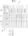
- FIG. 4 is a plan view of a portion corresponding to A1 of FIG. 1 according to an embodiment of the inventive concept.
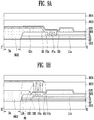
- FIG. 5A is a cross sectional view taken along line II-II' of FIG. 4
- FIG. 5B is a cross sectional view taken along line III-III' of FIG. 4
- FIG. 5C is a cross sectional view taken along line IV-IV' of FIG. 4 .
- the line part LP may include the first lines L1 and the second lines L2.
- the first lines L1 and the second lines L2 may be connected to each other one to one.
- the first lines L1 may generally extend in the second direction DR2 and be spaced apart from one another. Although it is illustrated in FIG. 4 that the first lines L1 are in parallel with one another, the first lines L1 are not limited thereto. As the first lines L1 extend in the second direction DR2, the distance among the first lines L1 may become smaller or larger. According to an embodiment of the inventive concept, the distance among the first lines L1 becomes smaller along the second direction DR2 and eventually the first lines L1 extend to be in parallel to maintain a predetermined distance.
- Each of the first lines L1 may have a first pad P1 at the end portion in the second direction DR2.
- a width of the portion including the first pads P1 e.g., a second width W2
- a width of the portion that does not include the first pads P1 e.g., a first width W1
- the second width W2 may be greater than the first width W1.
- a relatively larger width of the first pads P1 may facilitate contact with second pads P2.
- the second width W2 may be substantially equal to the first width W1.
- the first lines L1 may include first sub-lines L1a and second sub-lines L1b.
- a plurality of first sub-lines L1a and a plurality of second sub-lines L1b may be provided and alternately arranged in the first direction DR1.
- the first sub-lines L1a may be odd numbered lines of the first lines L1
- the second sub-lines L1b may be even numbered line of the first lines L1.
- the first sub-lines L1a may the even numbered line of the first lines L1
- the second sub-lines L1b may be odd numbered lines of the first lines L1.
- the first pads P1 include first sub-pads P1a and second sub-pads P1b that may be included in the end portions of the first sub-lines L1a and the second sub-lines L1b, respectively.
- the first sub-pads P1a and the second sub-pads P1b may be arranged with different distances from the display area DA along the second direction DR2. In other words, a minimum distance from the display area DA of the first sub-pad P1a may be shorter than a minimum distance from the display area DA of the second sub-pad P1b.
- the minimum distance from the display area DA of the first sub-pad P1a and the minimum distance from the display area DA of the second sub-pad P1b may be determined based on a length of the first sub-pads P1a and the second sub-pads P1b in the second direction DR2.
- the first sub-lines L1a and the second sub-lines L1b may be provided on the same layer. According to an embodiment of the inventive concept, the first sub-lines L1a and the second sub-lines L1b may be provided on the gate insulating layer GI, along with the gate electrode GE and the capacitor lower electrode LE. The first sub-lines L1a and the second sub-lines L1b may be formed in the same process as the gate electrode GE and the capacitor lower electrode LE with substantially the same material.
- the second lines L2 may substantially extend in the second direction DR2 and be separated from each other. Although the second lines L2 are illustrated in FIG. 4 to be parallel to each other, the second lines L2 are not limited thereto. As the second lines L2 extend in the second direction DR2, the distance among the second lines L2 may be widened or tapered.
- Each of the second lines L2 may have a second pad P2 in an end portion nearest to the bendable area BA.
- a portion of the second lines L2 without the second pad P2 has a third width W3.
- the second pad P2 has a fourth width W4.
- the fourth width W4 may be greater than the third width W3.
- the fourth width W4 of the second pads P2 may be relatively large to facilitate contact with the first pads P1.
- the fourth width W4 may be substantially equal to the third width W3 if needed.
- the second width W2 may be greater than the first width W1 and the fourth width W4 may be greater than the third width W3.
- widths of the first and second pads P1 and P2 e.g., W2 and W4 may be greater than widths of portions of the first and second lines L1 and L2 where the first and second pads are not overlapped (e.g., W1 and W3).
- the second width W2 may be substantially equal to the first width W1 and the fourth width W4 may be substantially equal to the third width W3.
- widths of the first and second pads P1 and P2 may be substantially the same as widths of portions of the first and second lines L1 and L2 where the first and second pads are not overlapped (e.g., W1 and W3).
- the second lines L2 may include third sub-lines L2a corresponding to the first sub-lines L1a of the first lines L1 and fourth sub-lines L2b corresponding to the second sub-lines L1b of the first lines L1.
- a plurality of third sub-lines L2a and a plurality of fourth sub-lines L2b may be alternately arranged along the first direction DR1.
- the third sub-lines L2a may be odd numbered lines of the second lines L2
- the fourth sub-lines L2b may be even numbered lines of the second lines L2.
- the third sub-lines L2a may be even numbered line of the second lines L2
- the fourth sub-lines L2b may be odd numbered lines of the second lines L2.
- the second pads P2 include third sub-pads P2a and fourth sub-pads P2b.
- the third sub-lines L2a and the fourth sub-lines L2b may include the third sub-pads P2a and the fourth sub-pads P2b, respectively, in the end portions nearest to the bendable area BA.
- the third sub-pads P2a may correspond to the first sub-pads P1a of the first sub-lines L1a
- the fourth sub-pads P2b may correspond to the second sub-pads P1b of the second sub-lines L1b.
- the third sub-pads P2a may overlap with the first sub-pads P1a and the fourth sub-pads P2b may overlap with the second sub-pads P1b.
- the third sub-pads P2a and the fourth sub-pads P2b may correspond to the positions of the first sub-pads P1a and the second sub-pads P1b, respectively, and may be formed to have different distances from the display area DA along the second direction DR2.
- a shortest distance from the display area DA of the third sub-pads P2a may be shorter than a shortest distance from the display area of DA of the fourth sub-pads P2b.
- the third sub-lines L2a and the fourth sub-lines L2b may be provided on the same layer.
- the third sub-lines L2a and the fourth sub-lines L2b may be provided on the first insulating layer INS1 and the second insulating layer INS2, along with the source electrode SE and the drain electrode DE of the display area DA.
- the third sub-lines L2a and the fourth sub-lines L2b may be formed in the same process with substantially the same material as the source electrode SE and the drain electrode DE.
- a width of each of the second pads P2 may be substantially the same as a width of each of the first pads P1, or may be different. In FIG. 4 , for convenience of explanation, the width of the second pad P2 is slightly greater than the width of the first pad P1. For example, according to an embodiment of the inventive concept, the width of the second pad P2 may be substantially the same as the width of the first pad P1.
- the second lines L2 may be provided between the second insulating layer INS2 and the third insulating layer INS3.
- the second lines L2 and the first lines L1 may correspond one to one and extend in a direction in which the first lines L1 extend.
- the end portion of the first lines L1 and the end portion of the second lines L2 may overlap with each other.
- the first pad P1 of the first lines L1 and the second pad P2 of the second lines L2 may overlap with each other.
- a first contact hole CH1 penetrating through the insulating interlayer IL and the first insulating layer INS1 may be provided.
- the first contact hole CH1 may be provided in at least one or more of overlapping portions of the sub-pads. According to an embodiment of the inventive concept, three first contact holes CH1 are illustrated in FIGS. 5A to 5C .
- a first hole HI may be provided in a position corresponding to the first sub-pads P1a and the second sub-pads P1b in the second insulating layer INS2.
- the first hole HI may expose the upper surfaces of the first sub-pads P1a and the second sub-pads P1b.
- the first hole HI may be formed to correspond to the first sub-pads P1a and the second sub-pads P1b and has a greater area than the area of each first sub-pad P1a and each second sub-pad P1b.
- a portion of the second pads P2 may be in contact with the first sub-pads P1a exposed by the first contact hole CH1 and the first hole HI
- the remaining portion of the second pads P2 e.g., the fourth sub-pads P2b
- the first sub-pads P1a and the third sub-pads P2a may be electrically connected to each other and the second sub-pads of P1b and the fourth sub-pads P2b may be electrically connected to each other.
- the edge of the second insulating layer INS2 is provided between the display area DA and a portion in which the first lines L1 overlap the second lines L2.
- the edge of the second insulating layer INS2 when viewed in a plan view, indicates an outermost boundary or side of the second insulating layer INS2 (e.g., the portion of the second insulating layer INS2 furthest from the bendable area BA as shown in FIG. 5A ), excluding boundaries or sides of the second insulating layer INS2 formed by the first hole H1.
- the edge of the second insulating layer INS2, the first sub-pads P1a and the third sub-pads P2a, and the second sub-pads P1b and the fourth pads P2b may be arranged sequentially along the second direction DR. Accordingly, an overlapping portion of the first sub-pads P1a and the third sub-pads P2a and an overlapping portion of the second sub-pads P1b and the fourth sub-pads P2b may be spaced from the edge of the second insulating layer INS2. According to an embodiment of the inventive concept, the edge of the second insulating layer INS2 may be spaced apart from the overlapping portion of the first sub-pads P1a and the third sub-pads P2a by at least one micrometer.
- the line part LP having the above structure may prevent shorts from occurring due to residue that may be generated during the formation of the line part LP.
- the overlapping portions of the first lines L1 and the second lines L2, e.g., the first pads P1 and the second pads P2 may be arranged to have the same minimum distance from the display area DA.
- the edge of the second insulating layer INS2 may partially overlap with at least a portion of the first pads P1 and the second pads P2. With respect to the first pads P1 and the second pads P2, since the width of the pads is greater than other portions of the lines so that the distance between adjacent pads is relatively small, the short distance between adjacent pads may result in residue.
- the first and the third sub-pads P1a and P2a and the second and fourth sub-pads P1b and P2b may be arranged with different distances from the display area DA along the second direction DR2, thus maximizing the space between adjacent pads.
- the second insulating layer INS2 may be manufactured by applying an organic material thereto, and a portion in which the second insulating layer INS2 is provided and a portion in which the second insulating layer INS2 is not provided may be placed at different heights from the substrate SUB.
- metal residue that was not yet removed may remain at the edge of the second insulating layer INS2. The metal residue may short the first and second lines L1 and L2 adjacent to each other, causing defects to occur in the display device.
- a first distance D1 is a minimum distance to the nearest of the second lines L2 in an area in which the fourth sub-pads P2b are not provided and a second distance D2 is a minimum distance to the nearest of the second lines L2 in an area in which the fourth sub-pads P2b are provided.
- the second distance D2 may be smaller than the first distance D1.
- the edge of the second insulating layer INS2 is spaced apart from the third sub-pads P2a where the space between the lines (e.g., the second lines L2) is relatively narrow, a short between the lines may be reduced or prevented even though metal residue may remain.
- the metal residue may be located in the conductive layer that is floated on the edge of the second insulating layer INS2.
- the first lines L1 may be arranged differently.
- repeat descriptions will be omitted to avoid redundancy.
- FIG. 6 is a plan view of a portion corresponding to A1 of a display device of FIG. 1 according to an embodiment of the present disclosure.
- FIG. 7A is a cross sectional view taken along line II-II' of FIG. 6
- FIG. 7B is a cross sectional view taken along line III-III' of FIG. 6
- FIG. 7C is a cross sectional view taken along line IV-IV' of FIG. 6 .
- the line part LP may include includes the first lines L1 and the second lines L2.
- the first lines L1 and the second lines L2 may be connected to correspond one to one.
- the first lines L1 may include the first sub-lines L1a and the second sub-lines L1b.
- the first sub-lines L1a and the second sub-lines L1b may be arranged alternately along the first direction DR1.
- the first sub-lines L1a and the second sub-lines L1b may include the first sub-pads P1a and the second sub-pads P1b, respectively, on end portions thereof.
- the first sub-lines L1a and the second sub-lines L1b are formed on different layers and are alternately arranged in the first direction DR1.
- the first sub-lines L1a may be provided on the gate insulating layer GI with the gate electrode GE of the display area DA and the capacitor lower electrode LE.
- the first sub-lines L1a may be formed in the same process as the gate electrode GE and the capacitor lower electrode LE with substantially the same material.
- the second sub-lines L1b may be provided on the insulating interlayer IL with the capacitor upper electrode UE of the display area DA.
- the second sub-lines L1b may be formed in the same process as the capacitor upper electrode UE with substantially the same material.
- the second lines L2 may include the third sub-lines L2a corresponding to the first sub-lines L1a and the fourth sub-lines L2b corresponding to the second sub-lines L1b.
- the third sub-lines L2a and the fourth sub-lines L2b may include the third sub-pads P2a and the fourth sub-pads P2b, respectively, at the end portions thereof nearest to the bendable area BA.
- the third sub-lines L2a and the fourth sub-lines L2b may be provided on the same layer.
- the third sub-lines L2a and the fourth sub-lines L2b may be provided on the first insulating layer INS1 and the second insulating layer INS2 with the source electrode SE and the drain electrode DE of the display area DA.
- the third sub-lines L2a and the fourth sub-lines L2b may be formed in the same process as the source electrode SE and the drain electrode DE with substantially the same material.
- the second lines L2 and the first lines L1 may correspond one on one.
- the first pad P1 of the first lines L1 and the second pad P2 of the second lines L may overlap with each other .
- the first contact hole CH1 penetrating through the insulating interlayer IL and the first insulating layer INS1 may be provided. At least one first contact hole CH1 may be provided. According to an embodiment of the inventive concept, three first contact holes CH1 are provided.
- a second contact hole CH2 penetrating through the first insulating layer INS1 may be provided. At least one second contact hole CH2 may be provided. According to an embodiment of the inventive concept, three second contact holes CH2 are provided.
- the first hole HI may be provided in a position corresponding to the first sub-pads P1a and the second sub-pads P1b in the second insulating layer INS2.
- a portion of the second pads P2 may be in contact with the first sub-pads P1a exposed by the first contact hole CH1 and the first hole HI
- a remaining portion of the second pads P2 e.g., the fourth sub-pads P2b
- the first sub-pads P1a and the third sub-pads P2a are electrically connected to each other and the second sub-pads P1b and the fourth sub-pads P2b are electrically connected to each other.
- the edge of the second insulating layer INS2 may be provided between the display area DA and the overlapping portion of the first lines L1 and the second lines L2.
- An overlapping portion of the first sub-pads P1a and the third sub-pads P2a and an overlapping portion of the second sub-pads P1b and the fourth sub-pads P2b may be spaced from the edge of the second insulating layer INS2.
- first sub-lines L1a and the second sub-lines L1b have the above described structure, a greater width may be established between adjacent lines among the first lines L1.
- first lines L1 are alternately formed on a single layer, spaces between adjacent first lines L1 is small.
- spaces between adjacent first lines L1 may be wider. As a result, the degree of freedom in designing the first lines L1 may increase.
- the most adjacent lines on the same layer may not be the second sub-lines L1b, but other first sub-lines L1a.
- the second sub-lines L1b may be on a different layer from the first sub-lines L1a.
- a third distance D3 may be a distance between adjacent first sub-lines L1a where the first sub-pad P1a is not provided.
- a fourth distance D4 may be a distance between adjacent first sub-lines L1a where the first sub-pad P1a is provided.
- the fourth distance D4 may be smaller than the third distance D3.
- spaces between adjacent lines may be larger since the first sub-lines L1a and the second sub-lines L1b are provided on different layers.
- more lines may be arranged in a narrower area because the lines are provided on different layers, and the degree of the freedom in design increases.
- shorts between adjacent lines may be reduced or prevented, as described above.
- FIG. 8 is a plan view of a portion corresponding to A1 of a display device of FIG. 1 according to an embodiment of the inventive concept.
- FIG. 9A is a cross sectional view taken along line II-II' of FIG. 8
- FIG. 9B is a cross sectional view taken along line III-III' of FIG. 8
- FIG. 9C is a cross sectional view taken along line IV-IV' of FIG. 8 .
- the first lines L1 may generally extend in the second direction DR2 and may be spaced apart from each other.
- Each of the first lines L1 has a first pad P1 in the second direction DR2.
- the first pads P1 may have a greater width than a width of the first lines L1 without the first pads P1.
- the first lines L1 may include the first sub-lines L1a and the second sub-lines L1b.
- the first sub-lines L1a and the second sub-lines L1b may be and alternately arranged along the first direction DR1.
- the first sub-lines L1a and the second sub-lines L1b may have the first sub-pads P1a and the second sub-pads P1b, respectively, at the end portions thereof.
- the first sub-lines L1a may be provided on the gate insulating layer GI with the gate electrode GE and the capacitor lower electrode LE.
- the first sub-lines L1a may be formed in the same process as the gate electrode GE and the capacitor lower electrode LE with substantially the same material.
- the second lines L2 may include the third sub-lines L2a corresponding to the first sub-lines L1a of the first lines L1 and the fourth sub-lines L2b corresponding to the second sub-lines L1b of the first lines L1.
- the third sub-lines L2a and the fourth sub-lines L2b may be alternately arranged along the first direction DR1.
- the third sub-lines L2a and the fourth sub-lines L2b may be provided on different layers.
- the third sub-lines L2a may be provided on the first insulating layer INS1 and the second insulating layer INS2 with the source electrode SE and the drain electrode DE of the display area DA.
- the third sub-lines L2a may be formed in the same process as the source electrode SE and the drain electrode DE with substantially the same material.
- the fourth sub-lines L2b may be provided on the third insulating layer INS3 with the connecting pattern CNP of the display area DA.
- the fourth sub-lines L2b may be formed in the same process as the connecting pattern CNP with substantially the same material.
- the third sub-lines L2a and the fourth sub-lines L2b may be formed on different layers and may be arranged sequentially and alternately in the first direction DR1. Accordingly, a large distance between adjacent second lines L2 may be established.
- space between adjacent second lines L2 is relatively narrow.
- the distance between adjacent second lines L2 may be wider. Therefore, the freedom of design of the second lines L2 may increase.
- the first contact hole CH1 penetrating the insulating interlayer IL and the first insulating layer INS1 may be provided in an area in which the first sub-pads P1a are formed.
- the second contact hole CH2 penetrating the first insulating layer INS1 may be provided in an area in which the second sub-pads P1b are formed.
- the first hole HI may be provided in a position corresponding to the first sub-pads P1a and the second sub-pads P1b in the second insulating layer INS2.
- the first hole HI may expose the upper surface of the first sub-pads P1a and the second sub-pads P1b.
- the third sub-pads P2a may contact the first sub-pads P1a exposed by the first contact hole CH1 and the first hole H1.
- a bridge pattern BR may be provided, which connects the second sub-pads P1b and the fourth sub-pads P2b.
- the bridge pattern BR may contact the second sub-pads P1b exposed by the second contact hole CH2 and the first hole HI.
- a third contact hole CH3 may be provided, which penetrates the passivation layer PSV and the third insulating layer INS3.
- One or more third contact holes CH3 may be provided. According to an embodiment of the inventive concept, three third contact holes CH3 are provided.
- the fourth sub-pads P2b may contact the bridge pattern BR through the third contact hole CH3, and the bridge pattern BR may contact the second sub-pads P1b through the second contact hole CH2.
- the second sub-pads P1b may be electrically connected to the fourth sub-pads P2b.
- the edge of the second insulating layer INS2 when viewed in a plan view, may be provided between the display area DA and an overlapping portion of the first lines L1 and second lines L2.
- the line part LP having such a structure may prevent shorts caused by residue that may be generated when the line part LP is formed.
- the most adjacent line on the same layer may not be the third sub-line L2a, but another fourth sub-line L2b because the third sub-lines L2a and the fourth sub-lines L2b are on different layers.
- a fifth distance D5 may be a distance between adjacent fourth sub-lines L2b where the fourth sub-pad P2b is not provided.
- a sixth distance D6 may be a distance between adjacent fourth sub-lines L2b where the fourth sub-pad P2b is provided. The sixth distance D6 may be smaller than the fifth distance D5.
- a distance between adjacent lines on the same layer may be larger.
- the space between adjacent lines is larger and the degree of design freedom increases accordingly.
- the first lines L1 and the second lines L2 may be provided on various layers, and may be combined with each other.
- the lines formed on different layers may be connected to one another through the contact holes.
- the second insulating layer INS2 may be provided in various forms.
- the hole that exposes a portion of the lines may have different shapes
- FIG. 10 is a cross sectional view taken along line I-I' of a display device of FIG. 1 according to an embodiment of the inventive concept.
- FIG. 11 is a plan view of a portion corresponding to A1 of a display device of FIG. 1 according to an embodiment of the inventive concept.
- FIG. 12A is a cross sectional view taken along line II-II' of FIG. 11
- FIG. 12B is a cross sectional view taken along line III-III' of FIG. 11
- FIG. 12C is a cross sectional view taken along line IV-IV' of FIG. 11 .
- the edge of the second insulating layer INS2 when view in a plan view, the edge of the second insulating layer INS2 may be provided between the display area DA and the overlapping portion of the first lines L1 and the second lines L2.
- the edge of the second insulating layer INS2 from the display area DA in the second direction DR2, the edge of the second insulating layer INS2, the first sub-pads P1a and the third sub-pads P2a, and the second sub-pads P1b and the fourth sub-pads P2b may be sequentially arranged.
- the second holes H2 may be provided in the second insulating layer INS2 in positions corresponding to the first sub-pads P1a and the second sub-pads P1b. Each second hole H2 may have a smaller area than the area of each first sub-pad P1a and the area of each second sub-pad P1b. In more detail, the second holes H2 may be provided in a position corresponding to a position in which the second contact holes CH2 are provided. In this case, when viewed in a plan view, the second holes H2 may overlap with the contact holes CH2. In FIGS. 12A to 12C , it is illustrated that the areas of the second holes H2 are slightly greater than those of the second contact holes CH2, but the inventive concept is not limited thereto. For example, the area of each of the second holes H2 may be substantially the same as the area of each of the contact holes CH2.
- the second insulating layer may be arranged differently to reduce or prevent shorts, which will be described below.
- FIG. 13 is a cross sectional view taken along line I-I' of a display device of FIG. 1 .
- FIG. 14 is a plan view of a portion corresponding to A1 of a display device of FIG. 1 .
- FIG. 15A is a cross sectional view taken along line II-II' of FIG. 14
- FIG. 15B is a cross sectional view taken along line III-III' of FIG. 14
- FIG. 15C is a cross sectional view taken along line IV-IV' of FIG. 14 .
- the line part LP may include the first lines L1 and the second lines L2.
- the first lines L1 and the second lines L2 may be connected to each other one to one.
- the first lines L1 may include the first sub-lines L1a and the second sub-lines L1b.
- the first sub-lines L1a and the second sub-lines L1b may be alternately arranged along the first direction DR1.
- the first sub-lines L1a and the second sub-lines L1b have the first sub-pads P1a and the second sub-pads P1b, respectively, on end portions thereof.
- the first sub-pads P1a and the second sub-pads P1b may be formed to have different distances from the display area DA in the second direction DR2.
- the first sub-lines L1a may be provided on the gate insulating layer GI with the gate electrode GE and the capacitor lower electrode LE of the display area DA.
- the first sub-lines L1a may be formed in the same process as the gate electrode GE and the capacitor lower electrode LE with substantially the same material.
- the second sub-lines L1b may be provided on the insulating interlayer IL with the capacitor upper electrode UE of the display area DA.
- the second sub-lines L1b may be formed in the same process as the capacitor upper electrode UE with substantially the same material
- the second lines L2 may be provided on the first insulating layer INS1 and the second insulating layer INS2.
- the second lines L2 and the first lines L1 may correspond one to one.
- the end portion of the first lines L1 and the end portion of the second lines L2 may overlap with each other.
- the first pads P1 of the first lines L1 and the second pads P2 of the second lines L2 may overlap with each other.
- the first contact hole CH1 penetrating the insulating interlayer IL and the first insulating layer INS1 may be provided.
- the second contact hole CH2 penetrating the first insulating layer INS1 may be provided.
- the third sub-lines L2a of the second lines L2 may correspond to the first sub-lines L1a and may be connected to the first sub-lines L1a through the contact hole CH1 penetrating the insulating interlayer IL and the first insulating layer INS1.
- the fourth sub-lines L2b of the second lines L2 may correspond to the second sub-lines L1b and may be connected to the second sub-lines L1b through the second contact hole CH2 penetrating the first insulating layer INS1.
- the first sub-pads P1a and the third sub-pads P2a may be electrically connected to each other and the second sub-pads P1b and the fourth sub-pad P2b may be electrically connected to each other.
- the edge of the second insulating layer INS2 may be spaced apart from the display area DA with the overlapping portion of the first lines L1 and second lines L2 interposed between.
- the display area DA, the overlapping portion of the first lines L1 and the second lines L2, and the edge of the second insulating layer INS2 may be sequentially arranged along the second direction DR2.
- the first sub-pads P1a and the third sub-pads P2a, the second sub-pads P1b and the fourth sub-pad P2b, and the edge of the second insulating layer INS2 may be sequentially arranged along the second direction DR2 from the display area DA.
- the edge of the second insulating layer INS2 are spaced apart a predetermined distance from the overlapping portion of the first lines L1 and the second lines L2. According to an embodiment of the inventive concept, the edge of the second insulating layer INS2 may be spaced apart from the ends of the second sub-pads P1b and the fourth sub-pads P2b by at least one micrometer.
- the second insulating layer INS2 is spaced apart from the overlapping portion of the first lines L1 and the second lines L2, unlike the above described embodiments, in the positions in which the first sub-pads P1a and the third sub-pads P2a are formed and the second sub-pads P1b and the fourth sub-pads P2b are formed, a hole may not be formed that exposes the first sub-pads P1a and the third sub-pads P2a and exposes the second sub-pads P1b and the fourth sub-pads P2b.
- each embodiment may be combined with each other.
- a display device may be employed in various types of electronic devices.
- the display device may be applied to devices such as a television, a laptop, a mobile phone, a smart phone, a smart pad, a portable media player (PMP), a personal digital assistant (PDA), etc.
- PMP portable media player
- PDA personal digital assistant
- a defect such as a disconnection or short during the manufacturing process of the display device may be minimized.
- a high quality display device may be provided.
Landscapes
- Physics & Mathematics (AREA)
- Nonlinear Science (AREA)
- Mathematical Physics (AREA)
- Chemical & Material Sciences (AREA)
- Crystallography & Structural Chemistry (AREA)
- General Physics & Mathematics (AREA)
- Optics & Photonics (AREA)
- Engineering & Computer Science (AREA)
- Microelectronics & Electronic Packaging (AREA)
- Electroluminescent Light Sources (AREA)
- Devices For Indicating Variable Information By Combining Individual Elements (AREA)
Claims (23)
- Anzeigevorrichtung, die Folgendes umfasst:ein Substrat (SUB) einschließend einen Anzeigebereich (DA) zum Anzeigen eines Bildes und einen auf mindestens einer Seite des Anzeigebereichs (DA) vorgesehenen Nichtanzeigebereich (NDA);eine Mehrzahl von Pixeln (PX), die auf dem Substrat (SUB) angeordnet und in einem Bereich, der dem Anzeigebereich (DA) entspricht, vorgesehen sind;eine erste Isolierschicht (INS1) mit einer ersten Öffnung (OPN2) in einem biegbaren Bereich (BA) des Nichtanzeigebereichs (NDA), wo die erste Isolierschicht (INS1) entfernt ist, wobei der biegbare Bereich (BA) zwischen einem ersten flachen Bereich (FA1) und einem zweiten flachen Bereich (FA2) der Anzeigevorrichtung angeordnet ist, wobei der biegbare Bereich (BA) eine Flexibilität hat und der erste und zweite flache Bereich (FA1, FA2) keine Flexibilität haben;eine zweite Isolierschicht (INS2), die die erste Öffnung (OPN2) füllt;erste Leitungen (L1), die auf dem Substrat (SUB) unter der ersten (INS1) und der zweiten (INS2) Isolierschicht vorgesehen und elektrisch mit der Mehrzahl von Pixeln (PX) verbunden sind; undzweite Leitungen (L2), die auf der ersten (INS1) und der zweiten (INS2) Isolierschicht vorgesehen und elektrisch mit den ersten Leitungen (L1) verbunden sind, wobei die zweiten Leitungen (L2) vom ersten flachen Bereich (FA1) zum zweiten flachen Bereich (FA2) über den biegbaren Bereich (BA) verlaufen,wobei ein Bereich, in dem die ersten Leitungen (L1) mit den zweiten Leitungen (L2) überlappen, von einem äußersten Rand der zweiten Isolierschicht (INS2) beabstandet ist, der in Draufsicht gesehen die erste Isolierschicht (INS1) überlappt, wobei der äußerste Rand der zweiten Isolierschicht (INS2), der zwischen dem Anzeigebereich (DA) und dem Bereich vorgesehen ist, in dem die ersten Leitungen (L1) mit den zweiten Leitungen (L2) überlappen, wobei die erste Isolierschicht (INS1) ein anorganisches Material umfasst und die zweite Isolierschicht (INS2) ein organisches Material umfasst.
- Anzeigevorrichtung nach Anspruch 1, wobei
die ersten Leitungen (L1) erste Pads (P1) aufweisen, die an einem Ende jeder ersten Leitung (L1) vorgesehen sind,
die zweiten Leitungen (L2) zweite Pads (P2) beinhalten, die an einem Ende jeder zweiten Leitung (L2) vorgesehen sind, und
die ersten Pads (P1) und die zweiten Pads (P2) in den Bereichen miteinander überlappen, in denen die ersten Leitungen (L1) in Draufsicht gesehen mit den zweiten Leitungen (L2) überlappen. - Anzeigevorrichtung nach Anspruch 2, wobei die erste Isolierschicht (INS1) mindestens ein Kontaktloch (CH1) in dem Bereich aufweist, in dem die ersten Pads (P1) mit den zweiten Pads (P2) überlappen, und die ersten Pads (P1) und die zweiten Pads (P2) durch das mindestens eine Kontaktloch (CH1) miteinander verbunden sind.
- Anzeigevorrichtung nach einem vorherigen Anspruch, die ferner eine Isolierzwischenschicht (IL) umfasst, die unterhalb der ersten Isolierschicht (INS1) vorgesehen ist und ebenso die erste Öffnung (OPN2) im biegbaren Bereich (BA) aufweist, wobei die zweite Isolierschicht (INS2) auch die erste Öffnung (OPN2) in der Isolierzwischenschicht (IL) füllt,
wobei die ersten Leitungen (L1) erste unterhalb der Isolierzwischenschicht (IL) vorgesehene Subleitungen (L1a) und auf der Isolierzwischenschicht (IL) vorgesehene zweite Subleitungen (L1b) aufweisen. - Anzeigevorrichtung nach Anspruch 4, wobei die ersten Subleitungen (L1a) und die zweiten Subleitungen (L1b) in Draufsicht gesehen abwechselnd angeordnet sind.
- Anzeigevorrichtung nach Anspruch 4 oder 5, wobei die zweiten Leitungen (L2) auf der zweiten Isolierschicht (INS2) vorgesehene dritte Subleitungen (L2a) und auf einer dritten Isolierschicht (INS3) vorgesehene vierte Subleitungen (L2b) einschließen, wobei die dritte Isolierschicht (INS3) auf der ersten Isolierschicht (INS1) und der zweiten Isolierschicht (INS2) vorgesehen ist.
- Anzeigevorrichtung nach Anspruch 6, wobei die dritten Subleitungen (L2a) und die vierten Subleitungen (L2b) in Draufsicht gesehen abwechselnd angeordnet sind.
- Anzeigevorrichtung nach Anspruch 7, wobei die ersten Subleitungen (L1a) mit den dritten Subleitungen (L2a) verbunden sind und die zweiten Subleitungen (L1b) mit den vierten Subleitungen (L2b) verbunden sind.
- Anzeigevorrichtung nach einem vorherigen Anspruch, wobei die zweite Isolierschicht (INS2) den biegbaren Bereich (BA) und einen Abschnitt des ersten und zweiten flachen Bereichs (FA1, FA2) neben dem biegbaren Bereich (BA) bedeckt.
- Anzeigevorrichtung nach Anspruch 3 oder einem von Anspruch 3 abhängigen Anspruch, wobei die zweite Isolierschicht (INS2) ein Loch (H1) zum Exponieren einer Oberseite der ersten Isolierschicht (INS1) in einer Position, die dem ersten und zweiten Pad (P1, P2) entspricht, in Draufsicht gesehen aufweist.
- Anzeigevorrichtung nach Anspruch 10, wobei das Loch (H1) einen größeren Bereich aufweist als das erste und zweite Pad (P1, P2).
- Anzeigevorrichtung nach Anspruch 10, wobei das Loch (H1) einen kleineren Bereich aufweist als das erste und zweite Pad (P1, P2).
- Anzeigevorrichtung nach Anspruch 12, wobei das Loch (H1) in einer Position, die dem mindestens einen Kontaktloch (CH1) der ersten Isolierschicht (INS1) entspricht, in Draufsicht gesehen vorgesehen ist.
- Anzeigevorrichtung nach Anspruch 2, wobei Breiten des ersten und zweiten Pads (P1, P2) größer sind als Breiten von Abschnitten der ersten und zweiten Leitungen (L1, L2), wo das erste und zweite Pad (P1, P2) nicht überlappt werden.
- Anzeigevorrichtung nach Anspruch 2, wobei Breiten des ersten und zweiten Pads (P1, P2) im Wesentlichen genauso groß sind wie Breiten von Abschnitten der ersten und zweiten Leitungen (L1, L2), wo das erste und zweite Pad (P1, P2) nicht überlappt werden.
- Anzeigevorrichtung nach Anspruch 2, wobei die zweiten Leitungen (L2) auf der zweiten Isolierschicht (INS2) vorgesehene dritte Subleitungen (L2a) und auf einer dritten Isolierschicht (INS3) vorgesehene vierte Subleitungen (L2b) umfassen, wobei die dritte Isolierschicht (INS3) auf der ersten Isolierschicht (INS1) und der zweiten Isolierschicht (INS2) vorgesehen ist.
- Anzeigevorrichtung nach Anspruch 16, wobei die dritten Subleitungen (L2a) und die vierten Subleitungen (L2b) in Draufsicht gesehen abwechselnd angeordnet sind.
- Anzeigevorrichtung nach Anspruch 1, die ferner eine dritte Isolierschicht (INS3) umfasst, die auf der ersten und der zweiten Isolierschicht (INS1, INS2) vorgesehen ist.
- Anzeigevorrichtung nach Anspruch 18, wobei die dritte Isolierschicht (INS3) eine zweite Öffnung (OPN1) entlang eines Randes des Anzeigebereichs (DA) aufweist, wobei die Anzeigevorrichtung eine Dichtungsschicht (SL) umfasst, die die durch die zweite Öffnung (OPN1) exponierte dritte Isolierschicht (INS3) abdichtet.
- Anzeigevorrichtung nach Anspruch 18 oder 19, wobei jedes Pixel (PX) Folgendes umfasst:ein aktives Muster (ACT), das auf dem Substrat (SUB) vorgesehen ist;eine Gate-Isolierschicht (GI), die auf dem aktiven Muster (ACT) vorgesehen ist;eine Gate-Elektrode (GE), die zwischen der Gate-Isolierschicht (GI) und der ersten Isolierschicht (INS1) vorgesehen ist;eine Source-Elektrode (SE) und eine Drain-Elektrode (DE), die auf der ersten Isolierschicht (INS1) vorgesehen sind;eine erste Elektrode (EL1), die auf der dritten Isolierschicht (INS3) vorgesehen und mit der Drain-Elektrode (DE) verbunden ist;eine organische Schicht (OL), die auf der ersten Elektrode (EL1) vorgesehen ist; undeine zweite Elektrode (EL2), die auf der organischen Schicht (OL) vorgesehen ist.
- Anzeigevorrichtung nach Anspruch 20, wobei die ersten Leitungen (L1) auf derselben Schicht und mit im Wesentlichen demselben Material vorgesehen sind wie die Gate-Elektrode (GE).
- Anzeigevorrichtung nach Anspruch 20 oder 21, wobei die zweiten Leitungen (L2) auf derselben Schicht und mit im Wesentlichen demselben Material vorgesehen sind wie die Source-Elektrode (SE) und die Drain-Elektrode (DE).
- Anzeigevorrichtung nach einem vorherigen Anspruch, wobei der äußerste Rand der zweiten Isolierschicht (INS2) und der biegbare Bereich (BA) in einer ersten Richtung (DR1) verlaufen und das Substrat (SUB) entlang einer Faltlinie gebogen ist, die sich in der ersten Richtung (DR1) erstreckt, wobei die Faltlinie im biegbaren Bereich (BA) ist.
Priority Applications (1)
| Application Number | Priority Date | Filing Date | Title |
|---|---|---|---|
| EP20181796.2A EP3734357A1 (de) | 2016-04-22 | 2017-01-31 | Anzeigevorrichtung |
Applications Claiming Priority (1)
| Application Number | Priority Date | Filing Date | Title |
|---|---|---|---|
| KR1020160049637A KR102587229B1 (ko) | 2016-04-22 | 2016-04-22 | 표시 장치 |
Related Child Applications (1)
| Application Number | Title | Priority Date | Filing Date |
|---|---|---|---|
| EP20181796.2A Division EP3734357A1 (de) | 2016-04-22 | 2017-01-31 | Anzeigevorrichtung |
Publications (2)
| Publication Number | Publication Date |
|---|---|
| EP3236309A1 EP3236309A1 (de) | 2017-10-25 |
| EP3236309B1 true EP3236309B1 (de) | 2020-06-24 |
Family
ID=57995029
Family Applications (2)
| Application Number | Title | Priority Date | Filing Date |
|---|---|---|---|
| EP17154020.6A Active EP3236309B1 (de) | 2016-04-22 | 2017-01-31 | Anzeigevorrichtung |
| EP20181796.2A Pending EP3734357A1 (de) | 2016-04-22 | 2017-01-31 | Anzeigevorrichtung |
Family Applications After (1)
| Application Number | Title | Priority Date | Filing Date |
|---|---|---|---|
| EP20181796.2A Pending EP3734357A1 (de) | 2016-04-22 | 2017-01-31 | Anzeigevorrichtung |
Country Status (4)
| Country | Link |
|---|---|
| US (3) | US10192896B2 (de) |
| EP (2) | EP3236309B1 (de) |
| KR (2) | KR102587229B1 (de) |
| CN (1) | CN107305305B (de) |
Families Citing this family (61)
| Publication number | Priority date | Publication date | Assignee | Title |
|---|---|---|---|---|
| US9911762B2 (en) * | 2015-12-03 | 2018-03-06 | Innolux Corporation | Display device |
| JP6756508B2 (ja) | 2016-04-04 | 2020-09-16 | 株式会社ジャパンディスプレイ | 表示装置 |
| KR102587229B1 (ko) | 2016-04-22 | 2023-10-12 | 삼성디스플레이 주식회사 | 표시 장치 |
| KR102687420B1 (ko) * | 2016-08-25 | 2024-07-22 | 엘지디스플레이 주식회사 | 표시패널 및 표시장치 |
| CN106972030B (zh) * | 2017-03-30 | 2019-09-03 | 京东方科技集团股份有限公司 | 一种柔性显示面板、显示装置及柔性显示面板的制作方法 |
| KR102386906B1 (ko) * | 2017-05-11 | 2022-04-18 | 삼성디스플레이 주식회사 | 표시 장치 |
| KR102465376B1 (ko) * | 2017-06-16 | 2022-11-10 | 삼성디스플레이 주식회사 | 표시 장치 및 표시 장치의 제조 방법 |
| JP6843710B2 (ja) * | 2017-07-12 | 2021-03-17 | 株式会社ジャパンディスプレイ | 表示装置、および表示装置の製造方法 |
| KR102393377B1 (ko) | 2017-08-07 | 2022-05-03 | 삼성디스플레이 주식회사 | 디스플레이 장치 |
| KR102341412B1 (ko) | 2017-08-29 | 2021-12-22 | 삼성디스플레이 주식회사 | 표시 장치 |
| WO2019064429A1 (ja) * | 2017-09-28 | 2019-04-04 | シャープ株式会社 | 表示装置 |
| KR102690983B1 (ko) * | 2018-02-13 | 2024-08-02 | 삼성디스플레이 주식회사 | 표시패널 및 그 제조방법 |
| KR102508445B1 (ko) * | 2017-12-28 | 2023-03-09 | 엘지디스플레이 주식회사 | 표시장치 |
| KR102414940B1 (ko) | 2017-10-31 | 2022-06-29 | 엘지디스플레이 주식회사 | 표시 장치 및 그의 제조방법 |
| CN109755256B (zh) * | 2017-11-01 | 2022-01-11 | 京东方科技集团股份有限公司 | 柔性显示面板及制备方法、柔性显示装置 |
| KR102476102B1 (ko) * | 2017-11-17 | 2022-12-12 | 삼성디스플레이 주식회사 | 표시 패널 및 이의 제조방법 |
| KR102606570B1 (ko) * | 2017-11-29 | 2023-11-30 | 삼성디스플레이 주식회사 | 표시패널 및 그 제조방법 |
| KR102018754B1 (ko) * | 2017-11-29 | 2019-09-05 | 엘지디스플레이 주식회사 | 플렉서블 표시 장치 |
| KR102416038B1 (ko) | 2017-11-30 | 2022-07-04 | 삼성디스플레이 주식회사 | 디스플레이 장치 및 그 제조 방법 |
| KR102436813B1 (ko) | 2017-12-08 | 2022-08-29 | 삼성디스플레이 주식회사 | 표시 패널 및 그 제조방법 |
| KR102552697B1 (ko) * | 2017-12-21 | 2023-07-05 | 엘지디스플레이 주식회사 | 플렉시블 발광 표시장치 |
| KR102526111B1 (ko) * | 2017-12-27 | 2023-04-25 | 엘지디스플레이 주식회사 | 표시 장치 |
| KR102524346B1 (ko) * | 2018-01-03 | 2023-04-25 | 삼성디스플레이 주식회사 | 표시 장치 및 표시 장치 제조 방법 |
| KR102535784B1 (ko) * | 2018-02-02 | 2023-05-24 | 삼성디스플레이 주식회사 | 표시 장치 및 그것의 제조 방법 |
| KR102550504B1 (ko) | 2018-02-09 | 2023-07-03 | 삼성전자주식회사 | 복수개의 배선층을 벤딩 영역에 포함하는 디스플레이 |
| US11404525B2 (en) * | 2018-03-01 | 2022-08-02 | Sharp Kabushiki Kaisha | Display device and method for manufacturing display device |
| US10734459B2 (en) | 2018-03-08 | 2020-08-04 | Samsung Display Co., Ltd. | Display device |
| KR20190117133A (ko) * | 2018-04-06 | 2019-10-16 | 삼성전자주식회사 | 벤딩 가능한 디스플레이를 포함하는 전자 장치 |
| US20190326329A1 (en) * | 2018-04-19 | 2019-10-24 | Innolux Corporation | Electronic device |
| KR102591811B1 (ko) * | 2018-05-18 | 2023-10-23 | 삼성디스플레이 주식회사 | 박막 트랜지스터 기판, 이의 제조 방법 및 이를 포함하는 표시 장치 |
| KR102772270B1 (ko) * | 2018-11-15 | 2025-02-24 | 삼성디스플레이 주식회사 | 표시 장치 |
| KR102761222B1 (ko) | 2018-11-26 | 2025-02-04 | 삼성디스플레이 주식회사 | 표시 장치 |
| KR102661283B1 (ko) * | 2018-11-26 | 2024-05-02 | 삼성디스플레이 주식회사 | 표시 기판, 이의 제조 방법, 및 이를 포함하는 표시 장치 |
| KR102748388B1 (ko) | 2018-11-28 | 2025-01-02 | 삼성디스플레이 주식회사 | 표시 장치 및 이의 제조 방법 |
| KR102726629B1 (ko) * | 2019-01-15 | 2024-11-07 | 삼성디스플레이 주식회사 | 표시 장치 |
| KR102770943B1 (ko) * | 2019-05-07 | 2025-02-24 | 삼성디스플레이 주식회사 | 표시장치 |
| CN110164933B (zh) * | 2019-05-24 | 2021-05-18 | 苏州清越光电科技股份有限公司 | 显示面板及显示装置 |
| CN110136651B (zh) * | 2019-06-12 | 2021-09-17 | 京东方科技集团股份有限公司 | 一种阵列基板、oled显示面板和显示装置 |
| CN110335875A (zh) * | 2019-07-02 | 2019-10-15 | 武汉华星光电技术有限公司 | 显示面板及其制作方法 |
| KR102903691B1 (ko) * | 2019-07-16 | 2025-12-24 | 삼성디스플레이 주식회사 | 표시장치 |
| KR102714129B1 (ko) | 2019-09-27 | 2024-10-10 | 삼성디스플레이 주식회사 | 표시 장치 및 표시 장치의 제조방법 |
| KR20210044356A (ko) * | 2019-10-14 | 2021-04-23 | 삼성디스플레이 주식회사 | 표시 장치 |
| KR20210059091A (ko) * | 2019-11-13 | 2021-05-25 | 삼성디스플레이 주식회사 | 표시 장치 |
| KR20210060715A (ko) * | 2019-11-18 | 2021-05-27 | 삼성디스플레이 주식회사 | 표시 장치 및 이의 제조 방법 |
| JP7680372B2 (ja) * | 2019-12-20 | 2025-05-20 | 京東方科技集團股▲ふん▼有限公司 | フレキシブル表示パネル及びその製造方法、並びにフレキシブル表示装置 |
| KR20210080687A (ko) * | 2019-12-20 | 2021-07-01 | 삼성디스플레이 주식회사 | 디스플레이 장치 |
| KR102756808B1 (ko) | 2019-12-27 | 2025-01-21 | 삼성디스플레이 주식회사 | 표시 장치 및 이의 제조 방법 |
| EP4095920B1 (de) * | 2020-01-22 | 2024-11-20 | BOE Technology Group Co., Ltd. | Anzeigetafel und anzeigevorrichtung |
| KR102867376B1 (ko) * | 2020-04-21 | 2025-10-02 | 삼성디스플레이 주식회사 | 표시장치 및 그 검사방법 |
| KR20210142808A (ko) * | 2020-05-18 | 2021-11-26 | 삼성디스플레이 주식회사 | 표시 장치 및 표시 장치의 제조방법 |
| CN111725436A (zh) * | 2020-06-09 | 2020-09-29 | 武汉华星光电半导体显示技术有限公司 | 基板及其制备方法、显示面板 |
| KR20200077477A (ko) * | 2020-06-18 | 2020-06-30 | 엘지디스플레이 주식회사 | 표시 장치 |
| CN111679525B (zh) * | 2020-06-22 | 2021-06-01 | 武汉华星光电技术有限公司 | 显示面板及其制作方法 |
| KR20220046750A (ko) * | 2020-10-07 | 2022-04-15 | 삼성디스플레이 주식회사 | 표시 장치 |
| US12219831B2 (en) * | 2020-10-14 | 2025-02-04 | Samsung Display Co., Ltd. | Display apparatus |
| KR102501143B1 (ko) * | 2020-10-27 | 2023-02-17 | 엘지디스플레이 주식회사 | 표시 장치의 제조방법 |
| KR20220099198A (ko) * | 2021-01-05 | 2022-07-13 | 삼성디스플레이 주식회사 | 표시 장치 및 그 제조 방법 |
| CN115552504B (zh) * | 2021-04-29 | 2025-02-25 | 京东方科技集团股份有限公司 | 显示面板 |
| US20240224652A1 (en) * | 2022-12-29 | 2024-07-04 | Lg Display Co., Ltd. | Display device |
| TWI830563B (zh) * | 2022-12-30 | 2024-01-21 | 友達光電股份有限公司 | 電子裝置 |
| KR20240156521A (ko) * | 2023-04-21 | 2024-10-30 | 삼성디스플레이 주식회사 | 표시 장치 |
Citations (1)
| Publication number | Priority date | Publication date | Assignee | Title |
|---|---|---|---|---|
| EP2814074A1 (de) * | 2013-05-28 | 2014-12-17 | LG Display Co., Ltd. | Flexible Anzeigevorrichtung und Herstellungsverfahren dafür |
Family Cites Families (50)
| Publication number | Priority date | Publication date | Assignee | Title |
|---|---|---|---|---|
| JP3272848B2 (ja) * | 1994-01-05 | 2002-04-08 | 株式会社日立製作所 | 液晶表示素子 |
| KR100831280B1 (ko) * | 2001-12-26 | 2008-05-22 | 엘지디스플레이 주식회사 | 액정표시장치 |
| US20050184392A1 (en) * | 2004-02-23 | 2005-08-25 | Kun-Hong Chen | Method for fabricating interconnect and interconnect fabricated thereby |
| US7764012B2 (en) * | 2004-04-16 | 2010-07-27 | Semiconductor Energy Laboratory Co., Ltd | Light emitting device comprising reduced frame portion, manufacturing method with improve productivity thereof, and electronic apparatus |
| CN1822385B (zh) | 2005-01-31 | 2013-02-06 | 株式会社半导体能源研究所 | 显示装置及含有其的电子设备 |
| JP4816297B2 (ja) * | 2006-07-21 | 2011-11-16 | 三菱電機株式会社 | 実装端子基板及びこれを用いた表示装置 |
| US20080204618A1 (en) * | 2007-02-22 | 2008-08-28 | Min-Kyung Jung | Display substrate, method for manufacturing the same, and display apparatus having the same |
| KR20080003962U (ko) | 2007-03-14 | 2008-09-19 | 이미지랩(주) | 플렉서블 멀티 디스플레이 장치 |
| KR100836472B1 (ko) | 2007-03-22 | 2008-06-09 | 삼성에스디아이 주식회사 | 반도체장치 및 그 제조방법 |
| CN101295717B (zh) | 2007-04-25 | 2010-07-14 | 北京京东方光电科技有限公司 | 薄膜晶体管面板及其制造方法 |
| TW201022779A (en) | 2008-12-12 | 2010-06-16 | Au Optronics Corp | Pixel array and manufacturing method thereof |
| KR101648806B1 (ko) * | 2009-07-20 | 2016-08-31 | 삼성디스플레이 주식회사 | 박막 트랜지스터 표시판 및 그 제조 방법 |
| KR101746198B1 (ko) | 2009-09-04 | 2017-06-12 | 가부시키가이샤 한도오따이 에네루기 켄큐쇼 | 표시장치 및 전자기기 |
| WO2011067964A1 (ja) | 2009-12-01 | 2011-06-09 | シャープ株式会社 | アクティブマトリクス基板及び表示装置 |
| KR101881020B1 (ko) | 2010-12-02 | 2018-07-24 | 삼성디스플레이 주식회사 | 액정 표시 장치 및 그 형성 방법 |
| TWI445170B (zh) | 2010-12-03 | 2014-07-11 | Au Optronics Corp | 有機發光二極體畫素陣列 |
| JP5720222B2 (ja) | 2010-12-13 | 2015-05-20 | ソニー株式会社 | 表示装置及び電子機器 |
| KR101802523B1 (ko) * | 2011-08-02 | 2017-11-28 | 엘지디스플레이 주식회사 | 유기전계발광표시장치와 이의 제조방법 |
| KR101885806B1 (ko) | 2012-05-01 | 2018-08-06 | 엘지디스플레이 주식회사 | 액정표시장치 및 그 제조방법 |
| KR101921965B1 (ko) * | 2012-08-07 | 2018-11-27 | 삼성디스플레이 주식회사 | 화소 및 이를 포함하는 유기발광 표시장치 |
| KR102025835B1 (ko) * | 2012-11-26 | 2019-11-27 | 삼성디스플레이 주식회사 | 표시 장치 및 유기 발광 표시 장치 |
| KR102222680B1 (ko) * | 2013-02-01 | 2021-03-03 | 엘지디스플레이 주식회사 | 플렉서블 디스플레이 기판, 플렉서블 유기 발광 표시 장치 및 플렉서블 유기 발광 표시 장치 제조 방법 |
| KR102018284B1 (ko) | 2013-02-28 | 2019-09-05 | 삼성디스플레이 주식회사 | 박막 트랜지스터 어레이 기판 및 이를 포함하는 유기 발광 표시 장치 |
| KR102076666B1 (ko) | 2013-04-11 | 2020-02-12 | 엘지디스플레이 주식회사 | 플렉서블 표시패널 |
| KR102047729B1 (ko) | 2013-04-30 | 2019-11-22 | 엘지디스플레이 주식회사 | 유기전계발광표시장치 및 그 제조방법 |
| KR102081287B1 (ko) * | 2013-06-07 | 2020-02-26 | 삼성디스플레이 주식회사 | 가요성 표시 장치 및 그 제조방법 |
| US9472507B2 (en) | 2013-06-17 | 2016-10-18 | Samsung Display Co., Ltd. | Array substrate and organic light-emitting display including the same |
| KR102085274B1 (ko) * | 2013-06-21 | 2020-03-06 | 삼성디스플레이 주식회사 | 유기 발광 표시 장치 |
| KR102086644B1 (ko) * | 2013-12-31 | 2020-03-09 | 엘지디스플레이 주식회사 | 플렉서블표시장치 및 이의 제조방법 |
| KR20160002018A (ko) * | 2014-06-30 | 2016-01-07 | 엘지디스플레이 주식회사 | 유기 발광 표시 장치 |
| KR102241248B1 (ko) * | 2014-09-23 | 2021-04-16 | 삼성디스플레이 주식회사 | 곡면형 표시 장치 |
| US9349758B2 (en) | 2014-09-30 | 2016-05-24 | Lg Display Co., Ltd. | Flexible display device with divided power lines and manufacturing method for the same |
| KR102199359B1 (ko) | 2014-10-13 | 2021-01-07 | 삼성디스플레이 주식회사 | 유기 발광 표시 장치 및 그 제조 방법 |
| US9535522B2 (en) | 2014-12-22 | 2017-01-03 | Lg Display Co., Ltd. | Flexible organic light emitting diode display device |
| KR102239481B1 (ko) | 2014-12-31 | 2021-04-13 | 엘지디스플레이 주식회사 | 디스플레이 장치 |
| KR102334553B1 (ko) | 2015-08-13 | 2021-12-03 | 엘지디스플레이 주식회사 | 플렉서블 표시장치 |
| US10516118B2 (en) | 2015-09-30 | 2019-12-24 | Semiconductor Energy Laboratory Co., Ltd. | Electronic device, display device, method for manufacturing the same, and system including a plurality of display devices |
| US10444877B2 (en) | 2015-12-27 | 2019-10-15 | Lg Display Co., Ltd. | Display device with touch sensor |
| KR102426742B1 (ko) | 2015-12-31 | 2022-07-27 | 엘지디스플레이 주식회사 | 어레이 기판 및 이를 포함하는 표시 장치 |
| US10354578B2 (en) | 2016-04-15 | 2019-07-16 | Samsung Display Co., Ltd. | Display device |
| KR102587229B1 (ko) | 2016-04-22 | 2023-10-12 | 삼성디스플레이 주식회사 | 표시 장치 |
| KR102457244B1 (ko) | 2016-05-19 | 2022-10-21 | 삼성디스플레이 주식회사 | 표시 장치 |
| JP6815159B2 (ja) | 2016-10-14 | 2021-01-20 | 株式会社ジャパンディスプレイ | 表示装置 |
| KR102615687B1 (ko) | 2016-11-15 | 2023-12-21 | 삼성디스플레이 주식회사 | 표시 장치 |
| KR102619425B1 (ko) | 2016-11-21 | 2023-12-29 | 엘지디스플레이 주식회사 | 표시장치 |
| KR102676492B1 (ko) | 2016-11-30 | 2024-06-18 | 엘지디스플레이 주식회사 | 박막 트랜지스터 및 이를 이용한 표시패널 |
| KR102793284B1 (ko) | 2017-02-21 | 2025-04-10 | 삼성디스플레이 주식회사 | 표시 장치 |
| JP6912080B2 (ja) | 2017-06-09 | 2021-07-28 | 株式会社Joled | 有機el表示パネル |
| KR102341412B1 (ko) | 2017-08-29 | 2021-12-22 | 삼성디스플레이 주식회사 | 표시 장치 |
| CN107978622B (zh) | 2017-11-22 | 2020-08-11 | 上海天马有机发光显示技术有限公司 | 一种阵列基板、显示面板和显示装置 |
-
2016
- 2016-04-22 KR KR1020160049637A patent/KR102587229B1/ko active Active
- 2016-10-14 US US15/293,779 patent/US10192896B2/en active Active
-
2017
- 2017-01-31 EP EP17154020.6A patent/EP3236309B1/de active Active
- 2017-01-31 EP EP20181796.2A patent/EP3734357A1/de active Pending
- 2017-02-24 CN CN201710102617.8A patent/CN107305305B/zh active Active
-
2019
- 2019-01-11 US US16/245,670 patent/US10886306B2/en active Active
-
2021
- 2021-01-04 US US17/140,521 patent/US11749690B2/en active Active
-
2023
- 2023-10-04 KR KR1020230132100A patent/KR102650168B1/ko active Active
Patent Citations (1)
| Publication number | Priority date | Publication date | Assignee | Title |
|---|---|---|---|---|
| EP2814074A1 (de) * | 2013-05-28 | 2014-12-17 | LG Display Co., Ltd. | Flexible Anzeigevorrichtung und Herstellungsverfahren dafür |
Also Published As
| Publication number | Publication date |
|---|---|
| US20210126020A1 (en) | 2021-04-29 |
| US11749690B2 (en) | 2023-09-05 |
| KR20170121392A (ko) | 2017-11-02 |
| EP3734357A1 (de) | 2020-11-04 |
| US20190148413A1 (en) | 2019-05-16 |
| KR102650168B1 (ko) | 2024-03-25 |
| US20170309651A1 (en) | 2017-10-26 |
| US10886306B2 (en) | 2021-01-05 |
| KR102587229B1 (ko) | 2023-10-12 |
| EP3236309A1 (de) | 2017-10-25 |
| US10192896B2 (en) | 2019-01-29 |
| CN107305305B (zh) | 2022-02-08 |
| KR20230147024A (ko) | 2023-10-20 |
| CN107305305A (zh) | 2017-10-31 |
Similar Documents
| Publication | Publication Date | Title |
|---|---|---|
| EP3236309B1 (de) | Anzeigevorrichtung | |
| KR102798596B1 (ko) | 표시 장치 | |
| EP3267489B1 (de) | Anzeigevorrichtung mit schutzstruktur | |
| KR20230154412A (ko) | 표시 장치 | |
| KR102675575B1 (ko) | 표시 장치 | |
| KR102733637B1 (ko) | 표시 장치 | |
| EP3680888A1 (de) | Anzeigevorrichtung mit lichtdurchlässigen bereichen | |
| KR102383745B1 (ko) | 표시 장치 | |
| CN110364548A (zh) | 显示设备 | |
| CN116744732A (zh) | 显示装置 | |
| KR20180051739A (ko) | 표시 장치 | |
| US12396322B2 (en) | Display device | |
| CN116347943B (zh) | 显示装置以及制造显示装置的方法 | |
| KR20230034702A (ko) | 표시 장치 | |
| KR20230102594A (ko) | 표시 장치 |
Legal Events
| Date | Code | Title | Description |
|---|---|---|---|
| PUAI | Public reference made under article 153(3) epc to a published international application that has entered the european phase |
Free format text: ORIGINAL CODE: 0009012 |
|
| STAA | Information on the status of an ep patent application or granted ep patent |
Free format text: STATUS: THE APPLICATION HAS BEEN PUBLISHED |
|
| AK | Designated contracting states |
Kind code of ref document: A1 Designated state(s): AL AT BE BG CH CY CZ DE DK EE ES FI FR GB GR HR HU IE IS IT LI LT LU LV MC MK MT NL NO PL PT RO RS SE SI SK SM TR |
|
| AX | Request for extension of the european patent |
Extension state: BA ME |
|
| STAA | Information on the status of an ep patent application or granted ep patent |
Free format text: STATUS: REQUEST FOR EXAMINATION WAS MADE |
|
| STAA | Information on the status of an ep patent application or granted ep patent |
Free format text: STATUS: EXAMINATION IS IN PROGRESS |
|
| 17P | Request for examination filed |
Effective date: 20180419 |
|
| RBV | Designated contracting states (corrected) |
Designated state(s): AL AT BE BG CH CY CZ DE DK EE ES FI FR GB GR HR HU IE IS IT LI LT LU LV MC MK MT NL NO PL PT RO RS SE SI SK SM TR |
|
| 17Q | First examination report despatched |
Effective date: 20180523 |
|
| RIC1 | Information provided on ipc code assigned before grant |
Ipc: H01L 21/768 20060101ALN20191128BHEP Ipc: H01L 51/00 20060101ALN20191128BHEP Ipc: G02F 1/1345 20060101AFI20191128BHEP Ipc: G02F 1/1362 20060101ALI20191128BHEP Ipc: H01L 27/12 20060101ALI20191128BHEP Ipc: H05B 33/08 20060101ALN20191128BHEP Ipc: H01L 27/32 20060101ALN20191128BHEP Ipc: G02F 1/1333 20060101ALI20191128BHEP |
|
| GRAP | Despatch of communication of intention to grant a patent |
Free format text: ORIGINAL CODE: EPIDOSNIGR1 |
|
| STAA | Information on the status of an ep patent application or granted ep patent |
Free format text: STATUS: GRANT OF PATENT IS INTENDED |
|
| INTG | Intention to grant announced |
Effective date: 20200116 |
|
| GRAS | Grant fee paid |
Free format text: ORIGINAL CODE: EPIDOSNIGR3 |
|
| GRAA | (expected) grant |
Free format text: ORIGINAL CODE: 0009210 |
|
| STAA | Information on the status of an ep patent application or granted ep patent |
Free format text: STATUS: THE PATENT HAS BEEN GRANTED |
|
| AK | Designated contracting states |
Kind code of ref document: B1 Designated state(s): AL AT BE BG CH CY CZ DE DK EE ES FI FR GB GR HR HU IE IS IT LI LT LU LV MC MK MT NL NO PL PT RO RS SE SI SK SM TR |
|
| REG | Reference to a national code |
Ref country code: GB Ref legal event code: FG4D |
|
| REG | Reference to a national code |
Ref country code: CH Ref legal event code: EP |
|
| REG | Reference to a national code |
Ref country code: AT Ref legal event code: REF Ref document number: 1284479 Country of ref document: AT Kind code of ref document: T Effective date: 20200715 |
|
| REG | Reference to a national code |
Ref country code: DE Ref legal event code: R096 Ref document number: 602017018529 Country of ref document: DE |
|
| REG | Reference to a national code |
Ref country code: IE Ref legal event code: FG4D |
|
| PG25 | Lapsed in a contracting state [announced via postgrant information from national office to epo] |
Ref country code: NO Free format text: LAPSE BECAUSE OF FAILURE TO SUBMIT A TRANSLATION OF THE DESCRIPTION OR TO PAY THE FEE WITHIN THE PRESCRIBED TIME-LIMIT Effective date: 20200924 Ref country code: GR Free format text: LAPSE BECAUSE OF FAILURE TO SUBMIT A TRANSLATION OF THE DESCRIPTION OR TO PAY THE FEE WITHIN THE PRESCRIBED TIME-LIMIT Effective date: 20200925 Ref country code: FI Free format text: LAPSE BECAUSE OF FAILURE TO SUBMIT A TRANSLATION OF THE DESCRIPTION OR TO PAY THE FEE WITHIN THE PRESCRIBED TIME-LIMIT Effective date: 20200624 Ref country code: LT Free format text: LAPSE BECAUSE OF FAILURE TO SUBMIT A TRANSLATION OF THE DESCRIPTION OR TO PAY THE FEE WITHIN THE PRESCRIBED TIME-LIMIT Effective date: 20200624 Ref country code: SE Free format text: LAPSE BECAUSE OF FAILURE TO SUBMIT A TRANSLATION OF THE DESCRIPTION OR TO PAY THE FEE WITHIN THE PRESCRIBED TIME-LIMIT Effective date: 20200624 |
|
| REG | Reference to a national code |
Ref country code: LT Ref legal event code: MG4D |
|
| PG25 | Lapsed in a contracting state [announced via postgrant information from national office to epo] |
Ref country code: HR Free format text: LAPSE BECAUSE OF FAILURE TO SUBMIT A TRANSLATION OF THE DESCRIPTION OR TO PAY THE FEE WITHIN THE PRESCRIBED TIME-LIMIT Effective date: 20200624 Ref country code: BG Free format text: LAPSE BECAUSE OF FAILURE TO SUBMIT A TRANSLATION OF THE DESCRIPTION OR TO PAY THE FEE WITHIN THE PRESCRIBED TIME-LIMIT Effective date: 20200924 Ref country code: RS Free format text: LAPSE BECAUSE OF FAILURE TO SUBMIT A TRANSLATION OF THE DESCRIPTION OR TO PAY THE FEE WITHIN THE PRESCRIBED TIME-LIMIT Effective date: 20200624 Ref country code: LV Free format text: LAPSE BECAUSE OF FAILURE TO SUBMIT A TRANSLATION OF THE DESCRIPTION OR TO PAY THE FEE WITHIN THE PRESCRIBED TIME-LIMIT Effective date: 20200624 |
|
| REG | Reference to a national code |
Ref country code: NL Ref legal event code: MP Effective date: 20200624 |
|
| REG | Reference to a national code |
Ref country code: AT Ref legal event code: MK05 Ref document number: 1284479 Country of ref document: AT Kind code of ref document: T Effective date: 20200624 |
|
| PG25 | Lapsed in a contracting state [announced via postgrant information from national office to epo] |
Ref country code: AL Free format text: LAPSE BECAUSE OF FAILURE TO SUBMIT A TRANSLATION OF THE DESCRIPTION OR TO PAY THE FEE WITHIN THE PRESCRIBED TIME-LIMIT Effective date: 20200624 Ref country code: NL Free format text: LAPSE BECAUSE OF FAILURE TO SUBMIT A TRANSLATION OF THE DESCRIPTION OR TO PAY THE FEE WITHIN THE PRESCRIBED TIME-LIMIT Effective date: 20200624 |
|
| PG25 | Lapsed in a contracting state [announced via postgrant information from national office to epo] |
Ref country code: PT Free format text: LAPSE BECAUSE OF FAILURE TO SUBMIT A TRANSLATION OF THE DESCRIPTION OR TO PAY THE FEE WITHIN THE PRESCRIBED TIME-LIMIT Effective date: 20201026 Ref country code: ES Free format text: LAPSE BECAUSE OF FAILURE TO SUBMIT A TRANSLATION OF THE DESCRIPTION OR TO PAY THE FEE WITHIN THE PRESCRIBED TIME-LIMIT Effective date: 20200624 Ref country code: AT Free format text: LAPSE BECAUSE OF FAILURE TO SUBMIT A TRANSLATION OF THE DESCRIPTION OR TO PAY THE FEE WITHIN THE PRESCRIBED TIME-LIMIT Effective date: 20200624 Ref country code: EE Free format text: LAPSE BECAUSE OF FAILURE TO SUBMIT A TRANSLATION OF THE DESCRIPTION OR TO PAY THE FEE WITHIN THE PRESCRIBED TIME-LIMIT Effective date: 20200624 Ref country code: SM Free format text: LAPSE BECAUSE OF FAILURE TO SUBMIT A TRANSLATION OF THE DESCRIPTION OR TO PAY THE FEE WITHIN THE PRESCRIBED TIME-LIMIT Effective date: 20200624 Ref country code: CZ Free format text: LAPSE BECAUSE OF FAILURE TO SUBMIT A TRANSLATION OF THE DESCRIPTION OR TO PAY THE FEE WITHIN THE PRESCRIBED TIME-LIMIT Effective date: 20200624 Ref country code: IT Free format text: LAPSE BECAUSE OF FAILURE TO SUBMIT A TRANSLATION OF THE DESCRIPTION OR TO PAY THE FEE WITHIN THE PRESCRIBED TIME-LIMIT Effective date: 20200624 Ref country code: RO Free format text: LAPSE BECAUSE OF FAILURE TO SUBMIT A TRANSLATION OF THE DESCRIPTION OR TO PAY THE FEE WITHIN THE PRESCRIBED TIME-LIMIT Effective date: 20200624 |
|
| PG25 | Lapsed in a contracting state [announced via postgrant information from national office to epo] |
Ref country code: IS Free format text: LAPSE BECAUSE OF FAILURE TO SUBMIT A TRANSLATION OF THE DESCRIPTION OR TO PAY THE FEE WITHIN THE PRESCRIBED TIME-LIMIT Effective date: 20201024 Ref country code: SK Free format text: LAPSE BECAUSE OF FAILURE TO SUBMIT A TRANSLATION OF THE DESCRIPTION OR TO PAY THE FEE WITHIN THE PRESCRIBED TIME-LIMIT Effective date: 20200624 Ref country code: PL Free format text: LAPSE BECAUSE OF FAILURE TO SUBMIT A TRANSLATION OF THE DESCRIPTION OR TO PAY THE FEE WITHIN THE PRESCRIBED TIME-LIMIT Effective date: 20200624 |
|
| REG | Reference to a national code |
Ref country code: DE Ref legal event code: R097 Ref document number: 602017018529 Country of ref document: DE |
|
| PG25 | Lapsed in a contracting state [announced via postgrant information from national office to epo] |
Ref country code: DK Free format text: LAPSE BECAUSE OF FAILURE TO SUBMIT A TRANSLATION OF THE DESCRIPTION OR TO PAY THE FEE WITHIN THE PRESCRIBED TIME-LIMIT Effective date: 20200624 |
|
| PLBE | No opposition filed within time limit |
Free format text: ORIGINAL CODE: 0009261 |
|
| STAA | Information on the status of an ep patent application or granted ep patent |
Free format text: STATUS: NO OPPOSITION FILED WITHIN TIME LIMIT |
|
| 26N | No opposition filed |
Effective date: 20210325 |
|
| PG25 | Lapsed in a contracting state [announced via postgrant information from national office to epo] |
Ref country code: MC Free format text: LAPSE BECAUSE OF FAILURE TO SUBMIT A TRANSLATION OF THE DESCRIPTION OR TO PAY THE FEE WITHIN THE PRESCRIBED TIME-LIMIT Effective date: 20200624 Ref country code: SI Free format text: LAPSE BECAUSE OF FAILURE TO SUBMIT A TRANSLATION OF THE DESCRIPTION OR TO PAY THE FEE WITHIN THE PRESCRIBED TIME-LIMIT Effective date: 20200624 |
|
| REG | Reference to a national code |
Ref country code: CH Ref legal event code: PL |
|
| PG25 | Lapsed in a contracting state [announced via postgrant information from national office to epo] |
Ref country code: LU Free format text: LAPSE BECAUSE OF NON-PAYMENT OF DUE FEES Effective date: 20210131 |
|
| REG | Reference to a national code |
Ref country code: BE Ref legal event code: MM Effective date: 20210131 |
|
| PG25 | Lapsed in a contracting state [announced via postgrant information from national office to epo] |
Ref country code: LI Free format text: LAPSE BECAUSE OF NON-PAYMENT OF DUE FEES Effective date: 20210131 Ref country code: CH Free format text: LAPSE BECAUSE OF NON-PAYMENT OF DUE FEES Effective date: 20210131 |
|
| PG25 | Lapsed in a contracting state [announced via postgrant information from national office to epo] |
Ref country code: IE Free format text: LAPSE BECAUSE OF NON-PAYMENT OF DUE FEES Effective date: 20210131 |
|
| PG25 | Lapsed in a contracting state [announced via postgrant information from national office to epo] |
Ref country code: BE Free format text: LAPSE BECAUSE OF NON-PAYMENT OF DUE FEES Effective date: 20210131 |
|
| PG25 | Lapsed in a contracting state [announced via postgrant information from national office to epo] |
Ref country code: HU Free format text: LAPSE BECAUSE OF FAILURE TO SUBMIT A TRANSLATION OF THE DESCRIPTION OR TO PAY THE FEE WITHIN THE PRESCRIBED TIME-LIMIT; INVALID AB INITIO Effective date: 20170131 |
|
| P01 | Opt-out of the competence of the unified patent court (upc) registered |
Effective date: 20230516 |
|
| PG25 | Lapsed in a contracting state [announced via postgrant information from national office to epo] |
Ref country code: CY Free format text: LAPSE BECAUSE OF FAILURE TO SUBMIT A TRANSLATION OF THE DESCRIPTION OR TO PAY THE FEE WITHIN THE PRESCRIBED TIME-LIMIT Effective date: 20200624 |
|
| PG25 | Lapsed in a contracting state [announced via postgrant information from national office to epo] |
Ref country code: MK Free format text: LAPSE BECAUSE OF FAILURE TO SUBMIT A TRANSLATION OF THE DESCRIPTION OR TO PAY THE FEE WITHIN THE PRESCRIBED TIME-LIMIT Effective date: 20200624 |
|
| PG25 | Lapsed in a contracting state [announced via postgrant information from national office to epo] |
Ref country code: MT Free format text: LAPSE BECAUSE OF FAILURE TO SUBMIT A TRANSLATION OF THE DESCRIPTION OR TO PAY THE FEE WITHIN THE PRESCRIBED TIME-LIMIT Effective date: 20200624 |
|
| PG25 | Lapsed in a contracting state [announced via postgrant information from national office to epo] |
Ref country code: TR Free format text: LAPSE BECAUSE OF FAILURE TO SUBMIT A TRANSLATION OF THE DESCRIPTION OR TO PAY THE FEE WITHIN THE PRESCRIBED TIME-LIMIT Effective date: 20200624 |
|
| PGFP | Annual fee paid to national office [announced via postgrant information from national office to epo] |
Ref country code: GB Payment date: 20251222 Year of fee payment: 10 |
|
| PGFP | Annual fee paid to national office [announced via postgrant information from national office to epo] |
Ref country code: FR Payment date: 20251223 Year of fee payment: 10 |
|
| PGFP | Annual fee paid to national office [announced via postgrant information from national office to epo] |
Ref country code: DE Payment date: 20251222 Year of fee payment: 10 |