EP3236724A1 - Système électronique de puissance et véhicule en étant équipé - Google Patents
Système électronique de puissance et véhicule en étant équipé Download PDFInfo
- Publication number
- EP3236724A1 EP3236724A1 EP17166538.3A EP17166538A EP3236724A1 EP 3236724 A1 EP3236724 A1 EP 3236724A1 EP 17166538 A EP17166538 A EP 17166538A EP 3236724 A1 EP3236724 A1 EP 3236724A1
- Authority
- EP
- European Patent Office
- Prior art keywords
- contact
- contact surface
- electronic device
- load connection
- connection element
- Prior art date
- Legal status (The legal status is an assumption and is not a legal conclusion. Google has not performed a legal analysis and makes no representation as to the accuracy of the status listed.)
- Granted
Links
Images


Classifications
-
- B—PERFORMING OPERATIONS; TRANSPORTING
- B60—VEHICLES IN GENERAL
- B60R—VEHICLES, VEHICLE FITTINGS, OR VEHICLE PARTS, NOT OTHERWISE PROVIDED FOR
- B60R16/00—Electric or fluid circuits specially adapted for vehicles and not otherwise provided for; Arrangement of elements of electric or fluid circuits specially adapted for vehicles and not otherwise provided for
- B60R16/02—Electric or fluid circuits specially adapted for vehicles and not otherwise provided for; Arrangement of elements of electric or fluid circuits specially adapted for vehicles and not otherwise provided for electric constitutive elements
- B60R16/03—Electric or fluid circuits specially adapted for vehicles and not otherwise provided for; Arrangement of elements of electric or fluid circuits specially adapted for vehicles and not otherwise provided for electric constitutive elements for supply of electrical power to vehicle subsystems or for
- B60R16/0307—Electric or fluid circuits specially adapted for vehicles and not otherwise provided for; Arrangement of elements of electric or fluid circuits specially adapted for vehicles and not otherwise provided for electric constitutive elements for supply of electrical power to vehicle subsystems or for using generators driven by a machine different from the vehicle motor
-
- H—ELECTRICITY
- H10—SEMICONDUCTOR DEVICES; ELECTRIC SOLID-STATE DEVICES NOT OTHERWISE PROVIDED FOR
- H10W—GENERIC PACKAGES, INTERCONNECTIONS, CONNECTORS OR OTHER CONSTRUCTIONAL DETAILS OF DEVICES COVERED BY CLASS H10
- H10W72/00—Interconnections or connectors in packages
-
- B—PERFORMING OPERATIONS; TRANSPORTING
- B60—VEHICLES IN GENERAL
- B60K—ARRANGEMENT OR MOUNTING OF PROPULSION UNITS OR OF TRANSMISSIONS IN VEHICLES; ARRANGEMENT OR MOUNTING OF PLURAL DIVERSE PRIME-MOVERS IN VEHICLES; AUXILIARY DRIVES FOR VEHICLES; INSTRUMENTATION OR DASHBOARDS FOR VEHICLES; ARRANGEMENTS IN CONNECTION WITH COOLING, AIR INTAKE, GAS EXHAUST OR FUEL SUPPLY OF PROPULSION UNITS IN VEHICLES
- B60K1/00—Arrangement or mounting of electrical propulsion units
- B60K1/04—Arrangement or mounting of electrical propulsion units of the electric storage means for propulsion
-
- B—PERFORMING OPERATIONS; TRANSPORTING
- B60—VEHICLES IN GENERAL
- B60K—ARRANGEMENT OR MOUNTING OF PROPULSION UNITS OR OF TRANSMISSIONS IN VEHICLES; ARRANGEMENT OR MOUNTING OF PLURAL DIVERSE PRIME-MOVERS IN VEHICLES; AUXILIARY DRIVES FOR VEHICLES; INSTRUMENTATION OR DASHBOARDS FOR VEHICLES; ARRANGEMENTS IN CONNECTION WITH COOLING, AIR INTAKE, GAS EXHAUST OR FUEL SUPPLY OF PROPULSION UNITS IN VEHICLES
- B60K1/00—Arrangement or mounting of electrical propulsion units
- B60K1/02—Arrangement or mounting of electrical propulsion units comprising more than one electric motor
-
- B—PERFORMING OPERATIONS; TRANSPORTING
- B60—VEHICLES IN GENERAL
- B60K—ARRANGEMENT OR MOUNTING OF PROPULSION UNITS OR OF TRANSMISSIONS IN VEHICLES; ARRANGEMENT OR MOUNTING OF PLURAL DIVERSE PRIME-MOVERS IN VEHICLES; AUXILIARY DRIVES FOR VEHICLES; INSTRUMENTATION OR DASHBOARDS FOR VEHICLES; ARRANGEMENTS IN CONNECTION WITH COOLING, AIR INTAKE, GAS EXHAUST OR FUEL SUPPLY OF PROPULSION UNITS IN VEHICLES
- B60K7/00—Disposition of motor in, or adjacent to, traction wheel
- B60K7/0007—Disposition of motor in, or adjacent to, traction wheel the motor being electric
-
- B—PERFORMING OPERATIONS; TRANSPORTING
- B60—VEHICLES IN GENERAL
- B60R—VEHICLES, VEHICLE FITTINGS, OR VEHICLE PARTS, NOT OTHERWISE PROVIDED FOR
- B60R16/00—Electric or fluid circuits specially adapted for vehicles and not otherwise provided for; Arrangement of elements of electric or fluid circuits specially adapted for vehicles and not otherwise provided for
- B60R16/02—Electric or fluid circuits specially adapted for vehicles and not otherwise provided for; Arrangement of elements of electric or fluid circuits specially adapted for vehicles and not otherwise provided for electric constitutive elements
- B60R16/03—Electric or fluid circuits specially adapted for vehicles and not otherwise provided for; Arrangement of elements of electric or fluid circuits specially adapted for vehicles and not otherwise provided for electric constitutive elements for supply of electrical power to vehicle subsystems or for
-
- B—PERFORMING OPERATIONS; TRANSPORTING
- B66—HOISTING; LIFTING; HAULING
- B66F—HOISTING, LIFTING, HAULING OR PUSHING, NOT OTHERWISE PROVIDED FOR, e.g. DEVICES WHICH APPLY A LIFTING OR PUSHING FORCE DIRECTLY TO THE SURFACE OF A LOAD
- B66F9/00—Devices for lifting or lowering bulky or heavy goods for loading or unloading purposes
- B66F9/06—Devices for lifting or lowering bulky or heavy goods for loading or unloading purposes movable, with their loads, on wheels or the like, e.g. fork-lift trucks
- B66F9/075—Constructional features or details
- B66F9/07572—Propulsion arrangements
-
- H—ELECTRICITY
- H01—ELECTRIC ELEMENTS
- H01R—ELECTRICALLY-CONDUCTIVE CONNECTIONS; STRUCTURAL ASSOCIATIONS OF A PLURALITY OF MUTUALLY-INSULATED ELECTRICAL CONNECTING ELEMENTS; COUPLING DEVICES; CURRENT COLLECTORS
- H01R12/00—Structural associations of a plurality of mutually-insulated electrical connecting elements, specially adapted for printed circuits, e.g. printed circuit boards [PCB], flat or ribbon cables, or like generally planar structures, e.g. terminal strips, terminal blocks; Coupling devices specially adapted for printed circuits, flat or ribbon cables, or like generally planar structures; Terminals specially adapted for contact with, or insertion into, printed circuits, flat or ribbon cables, or like generally planar structures
- H01R12/70—Coupling devices
- H01R12/7005—Guiding, mounting, polarizing or locking means; Extractors
- H01R12/7011—Locking or fixing a connector to a PCB
- H01R12/7047—Locking or fixing a connector to a PCB with a fastener through a screw hole in the coupling device
-
- H—ELECTRICITY
- H01—ELECTRIC ELEMENTS
- H01R—ELECTRICALLY-CONDUCTIVE CONNECTIONS; STRUCTURAL ASSOCIATIONS OF A PLURALITY OF MUTUALLY-INSULATED ELECTRICAL CONNECTING ELEMENTS; COUPLING DEVICES; CURRENT COLLECTORS
- H01R12/00—Structural associations of a plurality of mutually-insulated electrical connecting elements, specially adapted for printed circuits, e.g. printed circuit boards [PCB], flat or ribbon cables, or like generally planar structures, e.g. terminal strips, terminal blocks; Coupling devices specially adapted for printed circuits, flat or ribbon cables, or like generally planar structures; Terminals specially adapted for contact with, or insertion into, printed circuits, flat or ribbon cables, or like generally planar structures
- H01R12/70—Coupling devices
- H01R12/82—Coupling devices connected with low or zero insertion force
-
- H—ELECTRICITY
- H01—ELECTRIC ELEMENTS
- H01R—ELECTRICALLY-CONDUCTIVE CONNECTIONS; STRUCTURAL ASSOCIATIONS OF A PLURALITY OF MUTUALLY-INSULATED ELECTRICAL CONNECTING ELEMENTS; COUPLING DEVICES; CURRENT COLLECTORS
- H01R13/00—Details of coupling devices of the kinds covered by groups H01R12/70 or H01R24/00 - H01R33/00
- H01R13/73—Means for mounting coupling parts to apparatus or structures, e.g. to a wall
-
- H—ELECTRICITY
- H05—ELECTRIC TECHNIQUES NOT OTHERWISE PROVIDED FOR
- H05K—PRINTED CIRCUITS; CASINGS OR CONSTRUCTIONAL DETAILS OF ELECTRIC APPARATUS; MANUFACTURE OF ASSEMBLAGES OF ELECTRICAL COMPONENTS
- H05K7/00—Constructional details common to different types of electric apparatus
- H05K7/14—Mounting supporting structure in casing or on frame or rack
- H05K7/1422—Printed circuit boards receptacles, e.g. stacked structures, electronic circuit modules or box like frames
- H05K7/1427—Housings
- H05K7/1432—Housings specially adapted for power drive units or power converters
- H05K7/14329—Housings specially adapted for power drive units or power converters specially adapted for the configuration of power bus bars
-
- H—ELECTRICITY
- H10—SEMICONDUCTOR DEVICES; ELECTRIC SOLID-STATE DEVICES NOT OTHERWISE PROVIDED FOR
- H10W—GENERIC PACKAGES, INTERCONNECTIONS, CONNECTORS OR OTHER CONSTRUCTIONAL DETAILS OF DEVICES COVERED BY CLASS H10
- H10W40/00—Arrangements for thermal protection or thermal control
- H10W40/10—Arrangements for heating
-
- H—ELECTRICITY
- H10—SEMICONDUCTOR DEVICES; ELECTRIC SOLID-STATE DEVICES NOT OTHERWISE PROVIDED FOR
- H10W—GENERIC PACKAGES, INTERCONNECTIONS, CONNECTORS OR OTHER CONSTRUCTIONAL DETAILS OF DEVICES COVERED BY CLASS H10
- H10W40/00—Arrangements for thermal protection or thermal control
- H10W40/20—Arrangements for cooling
- H10W40/22—Arrangements for cooling characterised by their shape, e.g. having conical or cylindrical projections
- H10W40/226—Arrangements for cooling characterised by their shape, e.g. having conical or cylindrical projections characterised by projecting parts, e.g. fins to increase surface area
-
- H—ELECTRICITY
- H10—SEMICONDUCTOR DEVICES; ELECTRIC SOLID-STATE DEVICES NOT OTHERWISE PROVIDED FOR
- H10W—GENERIC PACKAGES, INTERCONNECTIONS, CONNECTORS OR OTHER CONSTRUCTIONAL DETAILS OF DEVICES COVERED BY CLASS H10
- H10W78/00—Detachable holders for supporting packaged chips in operation
-
- H—ELECTRICITY
- H10—SEMICONDUCTOR DEVICES; ELECTRIC SOLID-STATE DEVICES NOT OTHERWISE PROVIDED FOR
- H10W—GENERIC PACKAGES, INTERCONNECTIONS, CONNECTORS OR OTHER CONSTRUCTIONAL DETAILS OF DEVICES COVERED BY CLASS H10
- H10W90/00—Package configurations
-
- B—PERFORMING OPERATIONS; TRANSPORTING
- B60—VEHICLES IN GENERAL
- B60K—ARRANGEMENT OR MOUNTING OF PROPULSION UNITS OR OF TRANSMISSIONS IN VEHICLES; ARRANGEMENT OR MOUNTING OF PLURAL DIVERSE PRIME-MOVERS IN VEHICLES; AUXILIARY DRIVES FOR VEHICLES; INSTRUMENTATION OR DASHBOARDS FOR VEHICLES; ARRANGEMENTS IN CONNECTION WITH COOLING, AIR INTAKE, GAS EXHAUST OR FUEL SUPPLY OF PROPULSION UNITS IN VEHICLES
- B60K7/00—Disposition of motor in, or adjacent to, traction wheel
- B60K2007/0061—Disposition of motor in, or adjacent to, traction wheel the motor axle being parallel to the wheel axle
-
- B—PERFORMING OPERATIONS; TRANSPORTING
- B60—VEHICLES IN GENERAL
- B60Y—INDEXING SCHEME RELATING TO ASPECTS CROSS-CUTTING VEHICLE TECHNOLOGY
- B60Y2200/00—Type of vehicle
- B60Y2200/10—Road Vehicles
- B60Y2200/14—Trucks; Load vehicles, Busses
-
- H—ELECTRICITY
- H01—ELECTRIC ELEMENTS
- H01R—ELECTRICALLY-CONDUCTIVE CONNECTIONS; STRUCTURAL ASSOCIATIONS OF A PLURALITY OF MUTUALLY-INSULATED ELECTRICAL CONNECTING ELEMENTS; COUPLING DEVICES; CURRENT COLLECTORS
- H01R2201/00—Connectors or connections adapted for particular applications
- H01R2201/26—Connectors or connections adapted for particular applications for vehicles
-
- H—ELECTRICITY
- H10—SEMICONDUCTOR DEVICES; ELECTRIC SOLID-STATE DEVICES NOT OTHERWISE PROVIDED FOR
- H10W—GENERIC PACKAGES, INTERCONNECTIONS, CONNECTORS OR OTHER CONSTRUCTIONAL DETAILS OF DEVICES COVERED BY CLASS H10
- H10W70/00—Package substrates; Interposers; Redistribution layers [RDL]
- H10W70/60—Insulating or insulated package substrates; Interposers; Redistribution layers
-
- H—ELECTRICITY
- H10—SEMICONDUCTOR DEVICES; ELECTRIC SOLID-STATE DEVICES NOT OTHERWISE PROVIDED FOR
- H10W—GENERIC PACKAGES, INTERCONNECTIONS, CONNECTORS OR OTHER CONSTRUCTIONAL DETAILS OF DEVICES COVERED BY CLASS H10
- H10W72/00—Interconnections or connectors in packages
- H10W72/50—Bond wires
- H10W72/531—Shapes of wire connectors
- H10W72/5363—Shapes of wire connectors the connected ends being wedge-shaped
-
- H—ELECTRICITY
- H10—SEMICONDUCTOR DEVICES; ELECTRIC SOLID-STATE DEVICES NOT OTHERWISE PROVIDED FOR
- H10W—GENERIC PACKAGES, INTERCONNECTIONS, CONNECTORS OR OTHER CONSTRUCTIONAL DETAILS OF DEVICES COVERED BY CLASS H10
- H10W72/00—Interconnections or connectors in packages
- H10W72/50—Bond wires
- H10W72/541—Dispositions of bond wires
- H10W72/5438—Dispositions of bond wires the bond wires having multiple connections on the same bond pad
-
- H—ELECTRICITY
- H10—SEMICONDUCTOR DEVICES; ELECTRIC SOLID-STATE DEVICES NOT OTHERWISE PROVIDED FOR
- H10W—GENERIC PACKAGES, INTERCONNECTIONS, CONNECTORS OR OTHER CONSTRUCTIONAL DETAILS OF DEVICES COVERED BY CLASS H10
- H10W72/00—Interconnections or connectors in packages
- H10W72/851—Dispositions of multiple connectors or interconnections
- H10W72/874—On different surfaces
-
- H—ELECTRICITY
- H10—SEMICONDUCTOR DEVICES; ELECTRIC SOLID-STATE DEVICES NOT OTHERWISE PROVIDED FOR
- H10W—GENERIC PACKAGES, INTERCONNECTIONS, CONNECTORS OR OTHER CONSTRUCTIONAL DETAILS OF DEVICES COVERED BY CLASS H10
- H10W90/00—Package configurations
- H10W90/10—Configurations of laterally-adjacent chips
Definitions
- the invention describes a power electronic device with a power semiconductor module and with a mounting device, and an electric vehicle hereby.
- An assembly unit for the electric power unit is known in a battery-powered truck, with an attachable to a support member of the truck mounting plate, a power electronics semiconductor plate and a semiconductor plate covering the housing cover, wherein the semiconductor plate is mounted directly on the mounting plate.
- the invention has for its object to present a power semiconductor module in the context of a power electronic device and a vehicle, the integration of the power semiconductor module is designed to be particularly effective in the vehicle.
- the power electronic device is formed with a power semiconductor module, with a contact spring, with a load connection element and with a mounting device, which is preferably designed as part of an electrically operated vehicle, wherein the power semiconductor module has a load connection element, which preferably protrudes outwardly from the interior of the power semiconductor module and preferably there has a first external contact surface, ie a contact surface for external connection, and wherein the load connection element has a second contact surface.
- An electrically conductive pressure contact connection, ie a non-positive contact between the first contact surface and the second contact surface is formed by means of the contact spring, wherein the necessary pressure on the contact spring is formed by the power semiconductor module to the mounting device non-positively, preferably by means of a screw connected is.
- the electrically conductive pressure contact connection is formed as a direct connection between the first contact surface and the second contact surface.
- the electrically conductive pressure contact connection is formed as an indirect connection between the first contact surface and the second contact surface, preferably by the contact spring between the first and second contact surface is arranged, and is electrically conductive, wherein a third contact surface of the contact spring is in direct electrical contact with the first contact surface and the fourth contact surface of the contact spring with the second contact surface.
- the mounting device has a pin, which preferably consists of an electrically insulating material.
- the pin can extend into the interior of the coil spring designed as a contact spring.
- the pin can pass through a recess of the load connection element.
- the pin can extend into the interior of the at least partially formed as a contact sleeve load connection element.
- the load connection element protrudes through a plastic housing of the power semiconductor module to the outside.
- the load connection element may be formed by a metallic base plate of the power semiconductor module, which preferably forms part of a cooling device forms outwardly, wherein it is further preferred if the load connection element is electrically insulated from the base plate.
- the electrically driven vehicle according to the invention is, inter alia, designed with a power electronic arrangement according to one of the preceding claims, with an energy storage device and with an electric drive motor as the main or auxiliary drive.
- the mounting device is an integral part of a drive axle.
- the energy storage device and the drive motor are electrically conductively connected to the power semiconductor module of the power electronic device by means of a plurality of load connection and associated load connection elements.
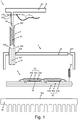
- FIG. 1 shows schematically, in exploded view, a first embodiment of a power electronic device according to the invention 1.
- This comprises a power semiconductor module 3, which in turn consists of a housing 30, a circuit substrate 4 and a metallic base plate, here formed as an air cooling device 52.
- the circuit carrier 4 is in this case arranged on the air cooling device 52 by means of a heat-conducting layer 502 and is covered or enclosed by the here cup-shaped housing 30 to the air cooling device 52.
- the circuit carrier 4 has a commercially available substrate 40 with a ceramic insulating body 402, which has a plurality of conductor tracks 404 on the side facing away from the air cooling device 52, and a metallic lamination 400 on the side facing the air cooling device 52.
- the conductor tracks 404 carry power semiconductor components 42 which are connected in a circuit-compatible manner by means of an internal connection device 44, which is likewise formed in the conventional manner by means of electrically conductive foils 440, 444 and electrically insulating foils 442.
- the housing 30 has on its side facing away from the air cooling device 52 two recesses 300, 302 on.
- the first recess 300 is used to carry out a load connection element 34, which thus protrudes outwardly from the interior of the power semiconductor module 3, while the second recess 302, the implementation of an auxiliary connection element 32, which is designed here as a spring.
- the load connection element 34 is embodied here as a current-carrying sleeve, more precisely as a hollow cylinder, and contacts a conductor track 404 of the substrate 40 in the interior of the power semiconductor module 3.
- a mounting device 8 as it may be an example of part of a truck.
- This mounting device 8 has an insulating body 82, in turn, integral with the insulating body formed, a pin 84 has.
- This pin 84 serves to arrange a contact body 70 designed as a contact lug of a load connection element 7.
- This contact lug has a continuous recess 700 with which it is arranged on the pin 84 of the insulating body 82 of the mounting device 8.
- From the contact lug is a connecting line 72 away, which serves as an example of the connection to a battery, more generally an energy storage device, or to an electric drive motor, more generally an electric machine.
- This embodiment of the load connection element 7 is purely exemplary, in principle all variants customary in the art, for example also in the form of current-conducting rails, are possible here.
- the pin 84 extends into the interior 60 of this contact spring 6 and leads them in their arrangement to the load connection element 7, more precisely to the contact lug and also to the load connection element 34 of the power semiconductor module 3.
- the electrically conductive connection between the Load connection element 34 and the load connection element 7 is produced by the power semiconductor module 3 is screwed onto the mounting device 8, that is non-positively connected thereto, see. also FIG. 5 , In this case, pressure is exerted on the contact spring 6 and this tensioned.
- the contact eye 70th course is the contact spring 6 made of conductive material, preferably metal.
- the contact spring 6 made of conductive material, preferably metal.
- FIG. 2 schematically shows an exploded view, a second embodiment of a power electronic device according to the invention 1.
- This comprises a power semiconductor module 3, which in turn has a circuit substrate 4 and a metallic base plate, here formed as a liquid cooling device 54.
- the circuit carrier 4 has a commercially available insulating substrate which, on the side facing away from the liquid cooling device, has a plurality of conductor tracks 404 which are opposite to the liquid cooling device by a Insulating body 402 are arranged electrically isolated.
- the conductor tracks 404 carry power semiconductor components 42, which are connected in a circuit-compatible manner by means of an internal connection device 42, which is formed here in a customary manner by means of wire bonding connections.
- the liquid cooling device 54 has a recess 500 through which a load connection element 34 extends. In this recess 56, a current sensor 36 is additionally arranged.
- the load connection element 34 is electrically insulated from the liquid cooling device 54 by means of an insulation device 344.
- the load connection element 34 has a screw thread 346 and a nut 348, with which it is arranged fixed to the cooling device 54.
- the nut 348 here forms the first contact surface 340, that of the load connection element 34.
- the load connection element 34 still has a pin-like section 384.
- a mounting device 8 is shown.
- This has an insulating body 82, which in turn, integrally formed with the insulating body, a pin 84 has.
- This pin 84 is aligned with the pin-like portion 384 of the load terminal member 34, without touching this in the assembled state, this being not restrictive.
- This pin-like portion 384 serves to arrange a contact body 70 designed as a contact eye of a load connection element 7.
- this contact eye has a continuous recess 700. From the contact hole 70 is as above FIG. 1 already described a connection line 72 away.
- this embodiment of the load connection element 7 is purely exemplary, in principle, all the usual variants are possible here.
- the contact spring 6 is arranged such that the pin 84 extends partially into the interior 60 of the formed as a helical spring contact spring 6.
- the journal-like section 384 of the load connection element 34 projects not only through the recess 700 of the contact lug 70 of the load connection element 7, but also into the interior 60 of the contact spring 6. As a result, the contact spring 6 and the load connection element 7 are already aligned during assembly of the arrangement.
- the contact spring 6 itself is not involved in the power supply, since the second contact surface 740, the one of the load connection element 7 is in direct electrically conductive contact with the first contact surface 340, that of the load connection element 34, whereby a direct electrically conductive pressure contact connection is formed.
- This direct electrically conductive pressure contact connection between the load connection element 34 and the load connection element 7 is produced by screwing the power semiconductor module 3 onto the mounting device 8, as indicated by the dashed line 10.
- pressure is exerted on the contact spring 6 and this tensioned.
- the contact spring 6 presses on the contact lug 70 of the load connection element 7, whereby its first contact surface 340 is pressed onto the second contact surface 740 of the load connection element 7.
- FIGS. 3 to 5 show schematically different variants to a third embodiment of a power electronic device according to the invention.
- a metallic base plate 50 of a power semiconductor module is shown, wherein a plurality of load connection elements 34 extend through recesses 500 of this base plate 50 and from this electrically isolated by means of an isolation device 344.
- an insulating body 82 of a mounting device 8 has a plurality of pins 84, wherein each pin 84 is associated with a load connection element 7.
- the contact device 70 of each load connection element 7 has a recess 700 through which the associated pin 84 passes.
- a contact spring 6 is arranged on each pin 84, wherein the pin 84 extends into the interior 60 of the formed as a helical spring contact spring 6.
- the load connection elements 34 are cylindrical, each with a centrally aligned pin-like portion 384 is formed.
- This pin-like portion 384 is arranged in alignment with the respectively associated pin 84 of the mounting device 8, wherein the pin 84 and the pin-like portion 384 extend from opposite sides into the interior 60 of the coil spring designed as a contact spring 6 and thus fix them in position.
- the electrically conductive pressure contact connection between the first contact surface 340, that of the load connection element 34, and the second contact surface 740, that of the load connection element 7, is here in each case formed as an indirect connection between the first contact surface 340 and the second contact surface 740 is, by the contact spring 6 is disposed between the first and second contact surface, and is electrically conductive, and wherein a third contact surface 640 of the contact spring 6 with the first contact surface 340 and the fourth contact surface 642 of the contact spring 6 with the second contact surface 740 respectively stand in direct electrical contact.
- contact surfaces in direct electrical contact with each other are here, as well as in general, always facing each other.
- the load connection elements 34 are cylindrical, each with a centrally aligned sleeve-like portion 386.
- this sleeve-like portion 386 protrudes a portion of the contact spring 6 completely into this sleeve-like portion.
- the pin 84 protrudes into the sleeve-like portion 386, while the contact spring 6 is in direct electrical contact with the top surface, which may have a circumferential recess and which forms the first contact surface 340.
- FIG. 5 shows a section of a mounting device 8 shown as it may be part of a truck in particular.
- This mounting device 8 has the already known insulating body 82 with integrally formed therefrom pin 84 and a metallic base body 80.
- the metallic base plate 50 of a power semiconductor module 3 has a plurality of recesses 500, only one of which is shown, extending through the load connection elements 34, which are each electrically insulated from the base plate 50 by means of an insulation device 344.
- the respective load connection element 34 in turn has a hollow cylindrical section 386 into which the pin 84 of the mounting device 8 extends.
- the contact spring and the load connection element is arranged by means of its recess of the contact body 6.
- the contact spring 6 is formed here from an electrically insulating material, or has at least one electrically insulating surface.
- the unstressed contact spring 6, as well as the respective load connection element 34 is arranged on the associated pin 84.
- the pin 84 extends through a recess 700 of the contact body 70 of the Load connection element 7 as well as through the interior 60 of the coil spring designed as a contact spring 6 therethrough.
- the mounting device 8 an internal thread and the base plate in alignment with a recess 56 for mounting a screw.
- sealing device 58 is shown. This is formed as a around all recesses 500 of the base plate 50 for the implementation of load connection elements 34 around extending Rundschnurdichtung, thus the base plate 50 to the mounting device 8, here without limiting the generality of the insulating material 82 seals out. In this case, individual seals would in particular be individual seals between the load connection elements and the base plate.
- FIG. 6 shows a further variant of the third embodiment of a power electronic device 1 according to the invention in a three-dimensional exploded view. Shown is a power semiconductor module 3 with a metallic base plate 50. On this professional components are arranged. Also shown are connectors 32 for auxiliary connections and a yoke 46 for the force support of pressure forces directed inwards into the power semiconductor module 3 and generated by the contact springs 6 on the load connection elements 34.
- the load connection elements 34 protrude through the base plate 50 in insulating sleeves 344.
- the load connection elements 34 are again designed as hollow cylinders with a first contact surface 340 on the cover surface of the hollow cylinder.
- the design of the mounting device 8, load connection device 7 and the contact spring 6, as well as their arrangement is basically how to FIG. 5 described.
- FIG. 7 schematically shows an inventive electrically powered vehicle 9, here specifically a truck, such as a forklift truck, in partial view. Shown in particular is the front axle of the forklift, each with a traction motor 90 per wheel.
- This power semiconductor module 3 is connected by means of load connection elements 7 with the traction motors 90 and with an energy storage device 92, that is to say with a battery, more precisely a rechargeable accumulator.
Landscapes
- Engineering & Computer Science (AREA)
- Mechanical Engineering (AREA)
- Transportation (AREA)
- Chemical & Material Sciences (AREA)
- Combustion & Propulsion (AREA)
- Structural Engineering (AREA)
- Microelectronics & Electronic Packaging (AREA)
- Civil Engineering (AREA)
- Life Sciences & Earth Sciences (AREA)
- Geology (AREA)
- Electric Propulsion And Braking For Vehicles (AREA)
- Inverter Devices (AREA)
- Cooling Or The Like Of Semiconductors Or Solid State Devices (AREA)
Priority Applications (1)
| Application Number | Priority Date | Filing Date | Title |
|---|---|---|---|
| EP18163958.4A EP3358921B1 (fr) | 2016-04-18 | 2017-04-13 | Dispositif électronique de puissance et véhicule correspondant |
Applications Claiming Priority (1)
| Application Number | Priority Date | Filing Date | Title |
|---|---|---|---|
| DE102016107083.1A DE102016107083B4 (de) | 2016-04-18 | 2016-04-18 | Leistungselektronische Anordnung und Fahrzeug hiermit |
Related Child Applications (2)
| Application Number | Title | Priority Date | Filing Date |
|---|---|---|---|
| EP18163958.4A Division EP3358921B1 (fr) | 2016-04-18 | 2017-04-13 | Dispositif électronique de puissance et véhicule correspondant |
| EP18163958.4A Division-Into EP3358921B1 (fr) | 2016-04-18 | 2017-04-13 | Dispositif électronique de puissance et véhicule correspondant |
Publications (2)
| Publication Number | Publication Date |
|---|---|
| EP3236724A1 true EP3236724A1 (fr) | 2017-10-25 |
| EP3236724B1 EP3236724B1 (fr) | 2020-12-30 |
Family
ID=58548611
Family Applications (2)
| Application Number | Title | Priority Date | Filing Date |
|---|---|---|---|
| EP17166538.3A Active EP3236724B1 (fr) | 2016-04-18 | 2017-04-13 | Système électronique de puissance et véhicule en étant équipé |
| EP18163958.4A Active EP3358921B1 (fr) | 2016-04-18 | 2017-04-13 | Dispositif électronique de puissance et véhicule correspondant |
Family Applications After (1)
| Application Number | Title | Priority Date | Filing Date |
|---|---|---|---|
| EP18163958.4A Active EP3358921B1 (fr) | 2016-04-18 | 2017-04-13 | Dispositif électronique de puissance et véhicule correspondant |
Country Status (5)
| Country | Link |
|---|---|
| US (1) | US9935032B2 (fr) |
| EP (2) | EP3236724B1 (fr) |
| KR (1) | KR102376002B1 (fr) |
| CN (2) | CN207320097U (fr) |
| DE (1) | DE102016107083B4 (fr) |
Cited By (3)
| Publication number | Priority date | Publication date | Assignee | Title |
|---|---|---|---|---|
| EP3432006A1 (fr) * | 2017-07-20 | 2019-01-23 | Audi Ag | Dispositif électronique avec un capteur de courant intégré dans un radiateur |
| WO2020064382A1 (fr) * | 2018-09-28 | 2020-04-02 | Knorr-Bremse Systeme für Nutzfahrzeuge GmbH | Dispositif de mise en contact pour effectuer la mise en contact électrique d'une carte de circuit imprimé avec un corps de bobine pour une électrovanne pour un système de freinage d'un véhicule, électrovanne dotée d'un dispositif de mise en contact et procédé de fabrication d'un dispositif de mise en contact |
| EP4074554A1 (fr) * | 2021-04-15 | 2022-10-19 | Robert Bosch GmbH | Dispositif de connexion pour un consommateur à tension continue haute tension, dispositif d'alimentation en énergie et essieu moteur électrique |
Families Citing this family (7)
| Publication number | Priority date | Publication date | Assignee | Title |
|---|---|---|---|---|
| DE102016107083B4 (de) * | 2016-04-18 | 2019-05-23 | Semikron Elektronik Gmbh & Co. Kg | Leistungselektronische Anordnung und Fahrzeug hiermit |
| CN111725679B (zh) * | 2016-12-12 | 2021-12-10 | 上海电巴新能源科技有限公司 | 电连接装置 |
| DE102017110722B4 (de) | 2017-05-17 | 2021-03-18 | Semikron Elektronik Gmbh & Co. Kg | Leistungselektronische Anordnung und elektrisches Fahrzeug hiermit |
| DE102017115883B4 (de) * | 2017-07-14 | 2020-04-02 | Semikron Elektronik Gmbh & Co. Kg | Leistungselektronisches Submodul mit Gleich- und Wechselspannungsanschlusselementen und Anordnung hiermit |
| DE102019111145A1 (de) * | 2019-04-30 | 2020-11-05 | Semikron Elektronik Gmbh & Co. Kg | Leistungshalbleitermodul und Verfahren zur Anordnung dieses Leistungshalbleitermoduls auf einem Motor |
| DE102019117476B4 (de) * | 2019-06-28 | 2024-03-14 | Semikron Elektronik Gmbh & Co. Kg | Leistungselektronische Schalteinrichtung mit einem Anschlusselement |
| CN118783154A (zh) | 2023-04-06 | 2024-10-15 | 台达电子工业股份有限公司 | 逆变器组装结构 |
Citations (6)
| Publication number | Priority date | Publication date | Assignee | Title |
|---|---|---|---|---|
| US20040245548A1 (en) * | 2003-04-10 | 2004-12-09 | Semikron Elektronik Gmbh | Power semiconductor module |
| EP1840961A2 (fr) * | 2006-02-13 | 2007-10-03 | SEMIKRON Elektronik GmbH & Co. KG | Module semi-conducteur de performance et son procédé de fabrication |
| US20090085188A1 (en) * | 2007-09-27 | 2009-04-02 | Mitsubishi Electric Corporation | Power semiconductor module |
| EP2239768A1 (fr) * | 2009-04-11 | 2010-10-13 | SEMIKRON Elektronik GmbH & Co. KG | Module semi-conducteur de puissance doté d'un dispositif de connexion et d'éléments de raccordement auxiliaire internes formés en tant que ressorts de contact |
| EP2378552A1 (fr) * | 2010-04-14 | 2011-10-19 | SEMIKRON Elektronik GmbH & Co. KG | Module semi-conducteur de puissance doté d'éléments de raccordement |
| DE102010053135A1 (de) | 2010-12-01 | 2012-06-06 | Jungheinrich Aktiengesellschaft | Montageeinheit für ein elektrisches Leistungsteil in einem Flurförderzeug |
Family Cites Families (10)
| Publication number | Priority date | Publication date | Assignee | Title |
|---|---|---|---|---|
| DE3225343A1 (de) | 1982-07-07 | 1984-01-12 | Fa. Carl Zeiss, 7920 Heidenheim | Verfahren und vorrichtung zur pruefung von linsen |
| JPS5918434U (ja) * | 1982-07-27 | 1984-02-04 | 株式会社東芝 | 半導体基板用加熱支持台 |
| SE9502498D0 (sv) * | 1995-07-07 | 1995-07-07 | Volvo Penta Ab | Cooling of heat-sensitive components |
| US5899323A (en) * | 1998-05-07 | 1999-05-04 | Eaton Corporation | Electrical switching apparatus with contact finger guide |
| DE19831829A1 (de) | 1998-07-15 | 2000-01-20 | Still Gmbh | Baueinheit aus einer elektrischen Maschine und einer Leistungselektronikeinheit |
| JP4706133B2 (ja) * | 2001-06-15 | 2011-06-22 | 株式会社豊田自動織機 | 産業車両における制御装置の冷却構造及びカウンタバランス型フォークリフトトラック |
| DE102008012570B4 (de) * | 2008-03-04 | 2014-02-13 | Infineon Technologies Ag | Leistungshalbleitermodul-System, Leistungshalbleitermodulanordnung und Verfahren zur Herstellung einer Leistungshalbleitermodulanordnung |
| DE102008034467B4 (de) * | 2008-07-24 | 2014-04-03 | Semikron Elektronik Gmbh & Co. Kg | Anordnung mit einem Leistungshalbleitermodul und mit einer Verbindungseinrichtung |
| US8466541B2 (en) * | 2011-10-31 | 2013-06-18 | Infineon Technologies Ag | Low inductance power module |
| DE102016107083B4 (de) * | 2016-04-18 | 2019-05-23 | Semikron Elektronik Gmbh & Co. Kg | Leistungselektronische Anordnung und Fahrzeug hiermit |
-
2016
- 2016-04-18 DE DE102016107083.1A patent/DE102016107083B4/de active Active
-
2017
- 2017-04-13 EP EP17166538.3A patent/EP3236724B1/fr active Active
- 2017-04-13 EP EP18163958.4A patent/EP3358921B1/fr active Active
- 2017-04-14 US US15/487,519 patent/US9935032B2/en active Active
- 2017-04-17 KR KR1020170049273A patent/KR102376002B1/ko active Active
- 2017-04-18 CN CN201720408628.4U patent/CN207320097U/zh not_active Withdrawn - After Issue
- 2017-04-18 CN CN201710252472.XA patent/CN107393893B/zh active Active
Patent Citations (6)
| Publication number | Priority date | Publication date | Assignee | Title |
|---|---|---|---|---|
| US20040245548A1 (en) * | 2003-04-10 | 2004-12-09 | Semikron Elektronik Gmbh | Power semiconductor module |
| EP1840961A2 (fr) * | 2006-02-13 | 2007-10-03 | SEMIKRON Elektronik GmbH & Co. KG | Module semi-conducteur de performance et son procédé de fabrication |
| US20090085188A1 (en) * | 2007-09-27 | 2009-04-02 | Mitsubishi Electric Corporation | Power semiconductor module |
| EP2239768A1 (fr) * | 2009-04-11 | 2010-10-13 | SEMIKRON Elektronik GmbH & Co. KG | Module semi-conducteur de puissance doté d'un dispositif de connexion et d'éléments de raccordement auxiliaire internes formés en tant que ressorts de contact |
| EP2378552A1 (fr) * | 2010-04-14 | 2011-10-19 | SEMIKRON Elektronik GmbH & Co. KG | Module semi-conducteur de puissance doté d'éléments de raccordement |
| DE102010053135A1 (de) | 2010-12-01 | 2012-06-06 | Jungheinrich Aktiengesellschaft | Montageeinheit für ein elektrisches Leistungsteil in einem Flurförderzeug |
Cited By (6)
| Publication number | Priority date | Publication date | Assignee | Title |
|---|---|---|---|---|
| EP3432006A1 (fr) * | 2017-07-20 | 2019-01-23 | Audi Ag | Dispositif électronique avec un capteur de courant intégré dans un radiateur |
| US10784180B2 (en) | 2017-07-20 | 2020-09-22 | Audi Ag | Electronics device having at least one component to be cooled |
| WO2020064382A1 (fr) * | 2018-09-28 | 2020-04-02 | Knorr-Bremse Systeme für Nutzfahrzeuge GmbH | Dispositif de mise en contact pour effectuer la mise en contact électrique d'une carte de circuit imprimé avec un corps de bobine pour une électrovanne pour un système de freinage d'un véhicule, électrovanne dotée d'un dispositif de mise en contact et procédé de fabrication d'un dispositif de mise en contact |
| CN112789769A (zh) * | 2018-09-28 | 2021-05-11 | 克诺尔商用车制动系统有限公司 | 用于使电路板与用于车辆制动装置的电磁阀的线圈体电接触的接触装置、具有接触装置的电磁阀和用于制造接触装置的方法 |
| US11837807B2 (en) | 2018-09-28 | 2023-12-05 | Knorr-Bremse Systeme Fuer Nutzfahrzeuge Gmbh | Contact-making device for making electrical contact with a printed circuit board by a coil former for a solenoid valve for a brake device for a vehicle, solenoid valve comprising a contact-making device and method for producing a contact-making device |
| EP4074554A1 (fr) * | 2021-04-15 | 2022-10-19 | Robert Bosch GmbH | Dispositif de connexion pour un consommateur à tension continue haute tension, dispositif d'alimentation en énergie et essieu moteur électrique |
Also Published As
| Publication number | Publication date |
|---|---|
| EP3358921A1 (fr) | 2018-08-08 |
| US9935032B2 (en) | 2018-04-03 |
| EP3236724B1 (fr) | 2020-12-30 |
| US20170301600A1 (en) | 2017-10-19 |
| KR102376002B1 (ko) | 2022-03-17 |
| KR20170119298A (ko) | 2017-10-26 |
| CN107393893B (zh) | 2022-04-08 |
| CN107393893A (zh) | 2017-11-24 |
| DE102016107083B4 (de) | 2019-05-23 |
| DE102016107083A1 (de) | 2017-11-02 |
| EP3358921B1 (fr) | 2021-01-20 |
| CN207320097U (zh) | 2018-05-04 |
Similar Documents
| Publication | Publication Date | Title |
|---|---|---|
| EP3236724B1 (fr) | Système électronique de puissance et véhicule en étant équipé | |
| EP3707737B1 (fr) | Dispositif d'électronique de puissance | |
| DE102015111204A1 (de) | Leistungselektronisches Modul mit Lastanschlusselementen | |
| DE102008059967A1 (de) | Batterie und Verfahren zur Herstellung einer Batterie mit einer in einem Batteriegehäuse angeordneten Wärmeleitplatte | |
| DE102010013025A1 (de) | Batterie und Verfahren zur Herstellung einer Batterie mit einer in einem Batteriegehäuse angeordneten Kühlplatte | |
| DE102008059947A1 (de) | Batterie mit einer in einem Batteriegehäuse angeordneten Wärmeleitplatte und daran direkt montierten elektronischen Bauelementen zum Temperieren der Batterie | |
| DE102014114828B4 (de) | Anordnung mit einem Leistungshalbleitermodul, mit einer Gleichspannungsverschienung und mit einer Kondensatoreinrichtung | |
| WO2017186803A2 (fr) | Ensemble conducteur et mécanisme de propulsion électrique mobile | |
| EP2716145B1 (fr) | Carte de circuits imprimés pour composants électriques et systèmes de cartes de circuits imprimés | |
| EP3223592A2 (fr) | Unité de commande électronique destinée au fonctionnement d'un moteur électrique comprenant une résistance de freinage | |
| DE102013209431B4 (de) | Leistungshalbleitermodul | |
| DE102020214912A1 (de) | Schaltvorrichtung, elektrischer Energiespeicher, Vorrichtung und Verfahren zum Herstellen einer Schaltvorrichtung | |
| DE102017110722B4 (de) | Leistungselektronische Anordnung und elektrisches Fahrzeug hiermit | |
| DE102017129707A1 (de) | Verfahren zur Herstellung eines leistungselektronischen Systems | |
| EP2341535B1 (fr) | Module semi-conducteur de puissance à contact de pression doté d'un accumulateur de pression hybride | |
| DE102014006346A1 (de) | Hochstromschalter | |
| EP2460760A1 (fr) | Unité de montage pour un élément de puissance électrique dans un chariot de manutention | |
| WO2008113323A1 (fr) | Connexion de mise à la masse | |
| DE102014003911A1 (de) | Batterie für ein Kraftfahrzeug | |
| DE102014206951A1 (de) | Batteriemodul mit wenigstens zwei parallel verschalteten Batteriezellen | |
| DE102011088402A1 (de) | Ladeeinrichtung mit elektrischem Steckverbinder für Elektrofahrzeug | |
| DE102013015756A1 (de) | Zellblock für eine Batterie | |
| DE102011077166B4 (de) | Vorrichtung zur Spannungsversorgung eines Kraftfahrzeugs | |
| EP4181640A1 (fr) | Composant électronique de puissance | |
| DE102015006201B4 (de) | Verbindungseinrichtung zum elektrischen Verbinden wenigstens zweier Energiespeicherelemente zum Speichern von elektrischer Energie |
Legal Events
| Date | Code | Title | Description |
|---|---|---|---|
| PUAI | Public reference made under article 153(3) epc to a published international application that has entered the european phase |
Free format text: ORIGINAL CODE: 0009012 |
|
| STAA | Information on the status of an ep patent application or granted ep patent |
Free format text: STATUS: THE APPLICATION HAS BEEN PUBLISHED |
|
| AK | Designated contracting states |
Kind code of ref document: A1 Designated state(s): AL AT BE BG CH CY CZ DE DK EE ES FI FR GB GR HR HU IE IS IT LI LT LU LV MC MK MT NL NO PL PT RO RS SE SI SK SM TR |
|
| AX | Request for extension of the european patent |
Extension state: BA ME |
|
| STAA | Information on the status of an ep patent application or granted ep patent |
Free format text: STATUS: REQUEST FOR EXAMINATION WAS MADE |
|
| 17P | Request for examination filed |
Effective date: 20180614 |
|
| RBV | Designated contracting states (corrected) |
Designated state(s): AL AT BE BG CH CY CZ DE DK EE ES FI FR GB GR HR HU IE IS IT LI LT LU LV MC MK MT NL NO PL PT RO RS SE SI SK SM TR |
|
| STAA | Information on the status of an ep patent application or granted ep patent |
Free format text: STATUS: EXAMINATION IS IN PROGRESS |
|
| 17Q | First examination report despatched |
Effective date: 20200207 |
|
| GRAP | Despatch of communication of intention to grant a patent |
Free format text: ORIGINAL CODE: EPIDOSNIGR1 |
|
| STAA | Information on the status of an ep patent application or granted ep patent |
Free format text: STATUS: GRANT OF PATENT IS INTENDED |
|
| RIC1 | Information provided on ipc code assigned before grant |
Ipc: B60K 1/04 20190101ALI20200909BHEP Ipc: H05K 7/14 20060101AFI20200909BHEP |
|
| INTG | Intention to grant announced |
Effective date: 20201002 |
|
| GRAS | Grant fee paid |
Free format text: ORIGINAL CODE: EPIDOSNIGR3 |
|
| GRAA | (expected) grant |
Free format text: ORIGINAL CODE: 0009210 |
|
| STAA | Information on the status of an ep patent application or granted ep patent |
Free format text: STATUS: THE PATENT HAS BEEN GRANTED |
|
| AK | Designated contracting states |
Kind code of ref document: B1 Designated state(s): AL AT BE BG CH CY CZ DE DK EE ES FI FR GB GR HR HU IE IS IT LI LT LU LV MC MK MT NL NO PL PT RO RS SE SI SK SM TR |
|
| REG | Reference to a national code |
Ref country code: GB Ref legal event code: FG4D Free format text: NOT ENGLISH |
|
| REG | Reference to a national code |
Ref country code: DE Ref legal event code: R096 Ref document number: 502017008802 Country of ref document: DE |
|
| REG | Reference to a national code |
Ref country code: AT Ref legal event code: REF Ref document number: 1351275 Country of ref document: AT Kind code of ref document: T Effective date: 20210115 |
|
| REG | Reference to a national code |
Ref country code: IE Ref legal event code: FG4D Free format text: LANGUAGE OF EP DOCUMENT: GERMAN |
|
| PG25 | Lapsed in a contracting state [announced via postgrant information from national office to epo] |
Ref country code: NO Free format text: LAPSE BECAUSE OF FAILURE TO SUBMIT A TRANSLATION OF THE DESCRIPTION OR TO PAY THE FEE WITHIN THE PRESCRIBED TIME-LIMIT Effective date: 20210330 Ref country code: RS Free format text: LAPSE BECAUSE OF FAILURE TO SUBMIT A TRANSLATION OF THE DESCRIPTION OR TO PAY THE FEE WITHIN THE PRESCRIBED TIME-LIMIT Effective date: 20201230 Ref country code: FI Free format text: LAPSE BECAUSE OF FAILURE TO SUBMIT A TRANSLATION OF THE DESCRIPTION OR TO PAY THE FEE WITHIN THE PRESCRIBED TIME-LIMIT Effective date: 20201230 Ref country code: GR Free format text: LAPSE BECAUSE OF FAILURE TO SUBMIT A TRANSLATION OF THE DESCRIPTION OR TO PAY THE FEE WITHIN THE PRESCRIBED TIME-LIMIT Effective date: 20210331 |
|
| PG25 | Lapsed in a contracting state [announced via postgrant information from national office to epo] |
Ref country code: LV Free format text: LAPSE BECAUSE OF FAILURE TO SUBMIT A TRANSLATION OF THE DESCRIPTION OR TO PAY THE FEE WITHIN THE PRESCRIBED TIME-LIMIT Effective date: 20201230 Ref country code: BG Free format text: LAPSE BECAUSE OF FAILURE TO SUBMIT A TRANSLATION OF THE DESCRIPTION OR TO PAY THE FEE WITHIN THE PRESCRIBED TIME-LIMIT Effective date: 20210330 Ref country code: SE Free format text: LAPSE BECAUSE OF FAILURE TO SUBMIT A TRANSLATION OF THE DESCRIPTION OR TO PAY THE FEE WITHIN THE PRESCRIBED TIME-LIMIT Effective date: 20201230 |
|
| REG | Reference to a national code |
Ref country code: NL Ref legal event code: MP Effective date: 20201230 |
|
| PG25 | Lapsed in a contracting state [announced via postgrant information from national office to epo] |
Ref country code: HR Free format text: LAPSE BECAUSE OF FAILURE TO SUBMIT A TRANSLATION OF THE DESCRIPTION OR TO PAY THE FEE WITHIN THE PRESCRIBED TIME-LIMIT Effective date: 20201230 |
|
| REG | Reference to a national code |
Ref country code: LT Ref legal event code: MG9D |
|
| PG25 | Lapsed in a contracting state [announced via postgrant information from national office to epo] |
Ref country code: PT Free format text: LAPSE BECAUSE OF FAILURE TO SUBMIT A TRANSLATION OF THE DESCRIPTION OR TO PAY THE FEE WITHIN THE PRESCRIBED TIME-LIMIT Effective date: 20210430 Ref country code: SK Free format text: LAPSE BECAUSE OF FAILURE TO SUBMIT A TRANSLATION OF THE DESCRIPTION OR TO PAY THE FEE WITHIN THE PRESCRIBED TIME-LIMIT Effective date: 20201230 Ref country code: RO Free format text: LAPSE BECAUSE OF FAILURE TO SUBMIT A TRANSLATION OF THE DESCRIPTION OR TO PAY THE FEE WITHIN THE PRESCRIBED TIME-LIMIT Effective date: 20201230 Ref country code: LT Free format text: LAPSE BECAUSE OF FAILURE TO SUBMIT A TRANSLATION OF THE DESCRIPTION OR TO PAY THE FEE WITHIN THE PRESCRIBED TIME-LIMIT Effective date: 20201230 Ref country code: EE Free format text: LAPSE BECAUSE OF FAILURE TO SUBMIT A TRANSLATION OF THE DESCRIPTION OR TO PAY THE FEE WITHIN THE PRESCRIBED TIME-LIMIT Effective date: 20201230 Ref country code: CZ Free format text: LAPSE BECAUSE OF FAILURE TO SUBMIT A TRANSLATION OF THE DESCRIPTION OR TO PAY THE FEE WITHIN THE PRESCRIBED TIME-LIMIT Effective date: 20201230 |
|
| PG25 | Lapsed in a contracting state [announced via postgrant information from national office to epo] |
Ref country code: PL Free format text: LAPSE BECAUSE OF FAILURE TO SUBMIT A TRANSLATION OF THE DESCRIPTION OR TO PAY THE FEE WITHIN THE PRESCRIBED TIME-LIMIT Effective date: 20201230 |
|
| PG25 | Lapsed in a contracting state [announced via postgrant information from national office to epo] |
Ref country code: IS Free format text: LAPSE BECAUSE OF FAILURE TO SUBMIT A TRANSLATION OF THE DESCRIPTION OR TO PAY THE FEE WITHIN THE PRESCRIBED TIME-LIMIT Effective date: 20210430 |
|
| REG | Reference to a national code |
Ref country code: DE Ref legal event code: R026 Ref document number: 502017008802 Country of ref document: DE |
|
| PLBI | Opposition filed |
Free format text: ORIGINAL CODE: 0009260 |
|
| PLAX | Notice of opposition and request to file observation + time limit sent |
Free format text: ORIGINAL CODE: EPIDOSNOBS2 |
|
| PG25 | Lapsed in a contracting state [announced via postgrant information from national office to epo] |
Ref country code: AL Free format text: LAPSE BECAUSE OF FAILURE TO SUBMIT A TRANSLATION OF THE DESCRIPTION OR TO PAY THE FEE WITHIN THE PRESCRIBED TIME-LIMIT Effective date: 20201230 |
|
| 26 | Opposition filed |
Opponent name: STILL GMBH Effective date: 20210930 |
|
| PG25 | Lapsed in a contracting state [announced via postgrant information from national office to epo] |
Ref country code: DK Free format text: LAPSE BECAUSE OF FAILURE TO SUBMIT A TRANSLATION OF THE DESCRIPTION OR TO PAY THE FEE WITHIN THE PRESCRIBED TIME-LIMIT Effective date: 20201230 Ref country code: MC Free format text: LAPSE BECAUSE OF FAILURE TO SUBMIT A TRANSLATION OF THE DESCRIPTION OR TO PAY THE FEE WITHIN THE PRESCRIBED TIME-LIMIT Effective date: 20201230 |
|
| PG25 | Lapsed in a contracting state [announced via postgrant information from national office to epo] |
Ref country code: LU Free format text: LAPSE BECAUSE OF NON-PAYMENT OF DUE FEES Effective date: 20210413 |
|
| REG | Reference to a national code |
Ref country code: BE Ref legal event code: MM Effective date: 20210430 |
|
| PG25 | Lapsed in a contracting state [announced via postgrant information from national office to epo] |
Ref country code: ES Free format text: LAPSE BECAUSE OF FAILURE TO SUBMIT A TRANSLATION OF THE DESCRIPTION OR TO PAY THE FEE WITHIN THE PRESCRIBED TIME-LIMIT Effective date: 20201230 Ref country code: LI Free format text: LAPSE BECAUSE OF NON-PAYMENT OF DUE FEES Effective date: 20210430 Ref country code: CH Free format text: LAPSE BECAUSE OF NON-PAYMENT OF DUE FEES Effective date: 20210430 |
|
| PLBB | Reply of patent proprietor to notice(s) of opposition received |
Free format text: ORIGINAL CODE: EPIDOSNOBS3 |
|
| PG25 | Lapsed in a contracting state [announced via postgrant information from national office to epo] |
Ref country code: SI Free format text: LAPSE BECAUSE OF FAILURE TO SUBMIT A TRANSLATION OF THE DESCRIPTION OR TO PAY THE FEE WITHIN THE PRESCRIBED TIME-LIMIT Effective date: 20201230 |
|
| PG25 | Lapsed in a contracting state [announced via postgrant information from national office to epo] |
Ref country code: IE Free format text: LAPSE BECAUSE OF NON-PAYMENT OF DUE FEES Effective date: 20210413 |
|
| PG25 | Lapsed in a contracting state [announced via postgrant information from national office to epo] |
Ref country code: IS Free format text: LAPSE BECAUSE OF FAILURE TO SUBMIT A TRANSLATION OF THE DESCRIPTION OR TO PAY THE FEE WITHIN THE PRESCRIBED TIME-LIMIT Effective date: 20210430 |
|
| PG25 | Lapsed in a contracting state [announced via postgrant information from national office to epo] |
Ref country code: BE Free format text: LAPSE BECAUSE OF NON-PAYMENT OF DUE FEES Effective date: 20210430 |
|
| PG25 | Lapsed in a contracting state [announced via postgrant information from national office to epo] |
Ref country code: HU Free format text: LAPSE BECAUSE OF FAILURE TO SUBMIT A TRANSLATION OF THE DESCRIPTION OR TO PAY THE FEE WITHIN THE PRESCRIBED TIME-LIMIT; INVALID AB INITIO Effective date: 20170413 |
|
| REG | Reference to a national code |
Ref country code: AT Ref legal event code: MM01 Ref document number: 1351275 Country of ref document: AT Kind code of ref document: T Effective date: 20220413 |
|
| PG25 | Lapsed in a contracting state [announced via postgrant information from national office to epo] |
Ref country code: NL Free format text: LAPSE BECAUSE OF NON-PAYMENT OF DUE FEES Effective date: 20201230 Ref country code: CY Free format text: LAPSE BECAUSE OF FAILURE TO SUBMIT A TRANSLATION OF THE DESCRIPTION OR TO PAY THE FEE WITHIN THE PRESCRIBED TIME-LIMIT Effective date: 20201230 |
|
| PG25 | Lapsed in a contracting state [announced via postgrant information from national office to epo] |
Ref country code: SM Free format text: LAPSE BECAUSE OF FAILURE TO SUBMIT A TRANSLATION OF THE DESCRIPTION OR TO PAY THE FEE WITHIN THE PRESCRIBED TIME-LIMIT Effective date: 20201230 Ref country code: AT Free format text: LAPSE BECAUSE OF NON-PAYMENT OF DUE FEES Effective date: 20220413 |
|
| PLBD | Termination of opposition procedure: decision despatched |
Free format text: ORIGINAL CODE: EPIDOSNOPC1 |
|
| PLBP | Opposition withdrawn |
Free format text: ORIGINAL CODE: 0009264 |
|
| REG | Reference to a national code |
Ref country code: DE Ref legal event code: R100 Ref document number: 502017008802 Country of ref document: DE |
|
| PLBM | Termination of opposition procedure: date of legal effect published |
Free format text: ORIGINAL CODE: 0009276 |
|
| 27C | Opposition proceedings terminated |
Effective date: 20230923 |
|
| PG25 | Lapsed in a contracting state [announced via postgrant information from national office to epo] |
Ref country code: MK Free format text: LAPSE BECAUSE OF FAILURE TO SUBMIT A TRANSLATION OF THE DESCRIPTION OR TO PAY THE FEE WITHIN THE PRESCRIBED TIME-LIMIT Effective date: 20201230 |
|
| PG25 | Lapsed in a contracting state [announced via postgrant information from national office to epo] |
Ref country code: MT Free format text: LAPSE BECAUSE OF FAILURE TO SUBMIT A TRANSLATION OF THE DESCRIPTION OR TO PAY THE FEE WITHIN THE PRESCRIBED TIME-LIMIT Effective date: 20201230 |
|
| PGFP | Annual fee paid to national office [announced via postgrant information from national office to epo] |
Ref country code: DE Payment date: 20250305 Year of fee payment: 9 |
|
| REG | Reference to a national code |
Ref country code: DE Ref legal event code: R081 Ref document number: 502017008802 Country of ref document: DE Owner name: SEMIKRON DANFOSS ELEKTRONIK GMBH & CO. KG, DE Free format text: FORMER OWNER: SEMIKRON ELEKTRONIK GMBH & CO. KG, 90431 NUERNBERG, DE |
|
| PG25 | Lapsed in a contracting state [announced via postgrant information from national office to epo] |
Ref country code: TR Free format text: LAPSE BECAUSE OF FAILURE TO SUBMIT A TRANSLATION OF THE DESCRIPTION OR TO PAY THE FEE WITHIN THE PRESCRIBED TIME-LIMIT Effective date: 20201230 |
|
| PGFP | Annual fee paid to national office [announced via postgrant information from national office to epo] |
Ref country code: GB Payment date: 20260312 Year of fee payment: 10 |
|
| PGFP | Annual fee paid to national office [announced via postgrant information from national office to epo] |
Ref country code: IT Payment date: 20260320 Year of fee payment: 10 |
|
| PGFP | Annual fee paid to national office [announced via postgrant information from national office to epo] |
Ref country code: FR Payment date: 20260309 Year of fee payment: 10 |