EP3237409B1 - Carbazoles comportant deux substituants dibenzofuranne ou dibenzothiophène - Google Patents
Carbazoles comportant deux substituants dibenzofuranne ou dibenzothiophène Download PDFInfo
- Publication number
- EP3237409B1 EP3237409B1 EP15801678.2A EP15801678A EP3237409B1 EP 3237409 B1 EP3237409 B1 EP 3237409B1 EP 15801678 A EP15801678 A EP 15801678A EP 3237409 B1 EP3237409 B1 EP 3237409B1
- Authority
- EP
- European Patent Office
- Prior art keywords
- formula
- atoms
- radicals
- group
- substituted
- Prior art date
- Legal status (The legal status is an assumption and is not a legal conclusion. Google has not performed a legal analysis and makes no representation as to the accuracy of the status listed.)
- Active
Links
- 0 CC*C1(CC*C)C(C=C(C)C(C)(C2*(CC)*2)C=C2)=C2C2=C1C=C*(*C)C=C2 Chemical compound CC*C1(CC*C)C(C=C(C)C(C)(C2*(CC)*2)C=C2)=C2C2=C1C=C*(*C)C=C2 0.000 description 10
- CRJISNQTZDMKQD-UHFFFAOYSA-N Brc1ccc2[o]c(cccc3)c3c2c1 Chemical compound Brc1ccc2[o]c(cccc3)c3c2c1 CRJISNQTZDMKQD-UHFFFAOYSA-N 0.000 description 1
- CNJPGTYPJKNGRF-UHFFFAOYSA-N N#Cc1ccc2[o]c(ccc(-[n]3c4cccc(-c(cc5)cc(c6c7ccc(-c(cc8)cc9c8[o]c8ccccc98)c6)c5[n]7-c5ccccc5)c4c4c3cccc4)c3)c3c2c1 Chemical compound N#Cc1ccc2[o]c(ccc(-[n]3c4cccc(-c(cc5)cc(c6c7ccc(-c(cc8)cc9c8[o]c8ccccc98)c6)c5[n]7-c5ccccc5)c4c4c3cccc4)c3)c3c2c1 CNJPGTYPJKNGRF-UHFFFAOYSA-N 0.000 description 1
- ZVJWLPMYUJVXIW-UHFFFAOYSA-N OB(c(cc1)cc(c2c3)c1[nH]c2ccc3-c(cc1c2c3cccc2)ccc1[n]3-c1ccccc1)O Chemical compound OB(c(cc1)cc(c2c3)c1[nH]c2ccc3-c(cc1c2c3cccc2)ccc1[n]3-c1ccccc1)O ZVJWLPMYUJVXIW-UHFFFAOYSA-N 0.000 description 1
- XQEMLFRVEDOFKJ-UHFFFAOYSA-N OB(c1cc(-c(cc2)cc3c2[o]c2ccccc32)cc(-[n]2c(cccc3)c3c3c2cccc3)c1)O Chemical compound OB(c1cc(-c(cc2)cc3c2[o]c2ccccc32)cc(-[n]2c(cccc3)c3c3c2cccc3)c1)O XQEMLFRVEDOFKJ-UHFFFAOYSA-N 0.000 description 1
- DSSBJZCMMKRJTF-UHFFFAOYSA-N OB(c1ccc2[o]c(cccc3)c3c2c1)O Chemical compound OB(c1ccc2[o]c(cccc3)c3c2c1)O DSSBJZCMMKRJTF-UHFFFAOYSA-N 0.000 description 1
- JHGWKDMJGVFYRA-UHFFFAOYSA-N c(cc1)cc(c2cc(-c3ccc4[o]c(cccc5)c5c4c3)ccc22)c1[n]2-c(cc1)ccc1-c(cc1)ccc1-c1c2[s]c(cccc3)c3c2ccc1 Chemical compound c(cc1)cc(c2cc(-c3ccc4[o]c(cccc5)c5c4c3)ccc22)c1[n]2-c(cc1)ccc1-c(cc1)ccc1-c1c2[s]c(cccc3)c3c2ccc1 JHGWKDMJGVFYRA-UHFFFAOYSA-N 0.000 description 1
- SKJYPPBPYSTDAB-UHFFFAOYSA-N c(cc1)cc2c1[o]c1c2c(-c(cc2)ccc2-[n](c(ccc(-c2c(c3ccccc3[o]3)c3ccc2)c2)c2c2c3)c2ccc3-c2cccc3c2c2ccccc2[s]3)ccc1 Chemical compound c(cc1)cc2c1[o]c1c2c(-c(cc2)ccc2-[n](c(ccc(-c2c(c3ccccc3[o]3)c3ccc2)c2)c2c2c3)c2ccc3-c2cccc3c2c2ccccc2[s]3)ccc1 SKJYPPBPYSTDAB-UHFFFAOYSA-N 0.000 description 1
- OMKAQSQLONEDBV-UHFFFAOYSA-N c(cc1)ccc1-[n](c(cccc1)c1c1c2)c1ccc2-c(cc1)cc(c2c3)c1[o]c2ccc3-c1ccc2[nH]c(cccc3)c3c2c1 Chemical compound c(cc1)ccc1-[n](c(cccc1)c1c1c2)c1ccc2-c(cc1)cc(c2c3)c1[o]c2ccc3-c1ccc2[nH]c(cccc3)c3c2c1 OMKAQSQLONEDBV-UHFFFAOYSA-N 0.000 description 1
- ZVRGLFLSZHHEMU-UHFFFAOYSA-N c(cc1)ccc1-[n](c1ccccc1c1c2)c1ccc2-c(cc1c2c3ccc(-c(cc4)cc5c4[o]c4c5cccc4)c2)ccc1[n]3-c1cc(-c(cc2)cc3c2[o]c2ccccc32)ccc1 Chemical compound c(cc1)ccc1-[n](c1ccccc1c1c2)c1ccc2-c(cc1c2c3ccc(-c(cc4)cc5c4[o]c4c5cccc4)c2)ccc1[n]3-c1cc(-c(cc2)cc3c2[o]c2ccccc32)ccc1 ZVRGLFLSZHHEMU-UHFFFAOYSA-N 0.000 description 1
- OJBVKPDQOCCYNY-UHFFFAOYSA-N c(cc1)ccc1-c1c(cc(cc2)-[n](c(cccc3)c3c3c4)c3ccc4-c(cc3)cc(c4cc(-c5cccc6c5[o]c5c6cccc5)ccc44)c3[n]4-c(cc3)ccc3-c3c4[o]c(cccc5)c5c4ccc3)c2nc(-c2ccccc2)n1 Chemical compound c(cc1)ccc1-c1c(cc(cc2)-[n](c(cccc3)c3c3c4)c3ccc4-c(cc3)cc(c4cc(-c5cccc6c5[o]c5c6cccc5)ccc44)c3[n]4-c(cc3)ccc3-c3c4[o]c(cccc5)c5c4ccc3)c2nc(-c2ccccc2)n1 OJBVKPDQOCCYNY-UHFFFAOYSA-N 0.000 description 1
- BUCOHQZWGBKJMJ-UHFFFAOYSA-N c(cc1)ccc1-c1c2[o]c(c(-c(cc3)ccc3-c(cc3c4cc(-c(cc5c6c7cccc6)ccc5[n]7-c5ccccc5)ccc44)ccc3[n]4-c(cc3)ccc3-c3cccc4c3[o]c3ccccc43)ccc3)c3c2ccc1 Chemical compound c(cc1)ccc1-c1c2[o]c(c(-c(cc3)ccc3-c(cc3c4cc(-c(cc5c6c7cccc6)ccc5[n]7-c5ccccc5)ccc44)ccc3[n]4-c(cc3)ccc3-c3cccc4c3[o]c3ccccc43)ccc3)c3c2ccc1 BUCOHQZWGBKJMJ-UHFFFAOYSA-N 0.000 description 1
- NSJLZOYHJZZETM-UHFFFAOYSA-N c(cc1c2c3)ccc1[o]c2ccc3-c(cc1c2cc(-c3c4[s]c5ccccc5c4ccc3)ccc22)ccc1[n]2-c1cccc(-c2cccc3c2[s]c2ccccc32)c1 Chemical compound c(cc1c2c3)ccc1[o]c2ccc3-c(cc1c2cc(-c3c4[s]c5ccccc5c4ccc3)ccc22)ccc1[n]2-c1cccc(-c2cccc3c2[s]c2ccccc32)c1 NSJLZOYHJZZETM-UHFFFAOYSA-N 0.000 description 1
- WZSXMVWPWTWCMI-UHFFFAOYSA-N c1ccc2[o]c3c(c4cc(-c(cc5)cc6c5[o]c5ccccc65)ccc4[n]4-c(cc5)ccc5-c5c6[o]c7ccccc7c6ccc5)c4ccc3c2c1 Chemical compound c1ccc2[o]c3c(c4cc(-c(cc5)cc6c5[o]c5ccccc65)ccc4[n]4-c(cc5)ccc5-c5c6[o]c7ccccc7c6ccc5)c4ccc3c2c1 WZSXMVWPWTWCMI-UHFFFAOYSA-N 0.000 description 1
Classifications
-
- C—CHEMISTRY; METALLURGY
- C07—ORGANIC CHEMISTRY
- C07D—HETEROCYCLIC COMPOUNDS
- C07D405/00—Heterocyclic compounds containing both one or more hetero rings having oxygen atoms as the only ring hetero atoms, and one or more rings having nitrogen as the only ring hetero atom
- C07D405/14—Heterocyclic compounds containing both one or more hetero rings having oxygen atoms as the only ring hetero atoms, and one or more rings having nitrogen as the only ring hetero atom containing three or more hetero rings
-
- C—CHEMISTRY; METALLURGY
- C07—ORGANIC CHEMISTRY
- C07D—HETEROCYCLIC COMPOUNDS
- C07D405/00—Heterocyclic compounds containing both one or more hetero rings having oxygen atoms as the only ring hetero atoms, and one or more rings having nitrogen as the only ring hetero atom
- C07D405/02—Heterocyclic compounds containing both one or more hetero rings having oxygen atoms as the only ring hetero atoms, and one or more rings having nitrogen as the only ring hetero atom containing two hetero rings
- C07D405/10—Heterocyclic compounds containing both one or more hetero rings having oxygen atoms as the only ring hetero atoms, and one or more rings having nitrogen as the only ring hetero atom containing two hetero rings linked by a carbon chain containing aromatic rings
-
- C—CHEMISTRY; METALLURGY
- C07—ORGANIC CHEMISTRY
- C07D—HETEROCYCLIC COMPOUNDS
- C07D409/00—Heterocyclic compounds containing two or more hetero rings, at least one ring having sulfur atoms as the only ring hetero atoms
- C07D409/14—Heterocyclic compounds containing two or more hetero rings, at least one ring having sulfur atoms as the only ring hetero atoms containing three or more hetero rings
-
- C—CHEMISTRY; METALLURGY
- C09—DYES; PAINTS; POLISHES; NATURAL RESINS; ADHESIVES; COMPOSITIONS NOT OTHERWISE PROVIDED FOR; APPLICATIONS OF MATERIALS NOT OTHERWISE PROVIDED FOR
- C09K—MATERIALS FOR MISCELLANEOUS APPLICATIONS, NOT PROVIDED FOR ELSEWHERE
- C09K11/00—Luminescent materials, e.g. electroluminescent or chemiluminescent
- C09K11/06—Luminescent materials, e.g. electroluminescent or chemiluminescent containing organic luminescent materials
-
- H—ELECTRICITY
- H10—SEMICONDUCTOR DEVICES; ELECTRIC SOLID-STATE DEVICES NOT OTHERWISE PROVIDED FOR
- H10K—ORGANIC ELECTRIC SOLID-STATE DEVICES
- H10K50/00—Organic light-emitting devices
- H10K50/10—OLEDs or polymer light-emitting diodes [PLED]
- H10K50/11—OLEDs or polymer light-emitting diodes [PLED] characterised by the electroluminescent [EL] layers
-
- H—ELECTRICITY
- H10—SEMICONDUCTOR DEVICES; ELECTRIC SOLID-STATE DEVICES NOT OTHERWISE PROVIDED FOR
- H10K—ORGANIC ELECTRIC SOLID-STATE DEVICES
- H10K50/00—Organic light-emitting devices
- H10K50/10—OLEDs or polymer light-emitting diodes [PLED]
- H10K50/14—Carrier transporting layers
- H10K50/15—Hole transporting layers
-
- H—ELECTRICITY
- H10—SEMICONDUCTOR DEVICES; ELECTRIC SOLID-STATE DEVICES NOT OTHERWISE PROVIDED FOR
- H10K—ORGANIC ELECTRIC SOLID-STATE DEVICES
- H10K50/00—Organic light-emitting devices
- H10K50/10—OLEDs or polymer light-emitting diodes [PLED]
- H10K50/14—Carrier transporting layers
- H10K50/16—Electron transporting layers
-
- H—ELECTRICITY
- H10—SEMICONDUCTOR DEVICES; ELECTRIC SOLID-STATE DEVICES NOT OTHERWISE PROVIDED FOR
- H10K—ORGANIC ELECTRIC SOLID-STATE DEVICES
- H10K50/00—Organic light-emitting devices
- H10K50/10—OLEDs or polymer light-emitting diodes [PLED]
- H10K50/17—Carrier injection layers
- H10K50/171—Electron injection layers
-
- H—ELECTRICITY
- H10—SEMICONDUCTOR DEVICES; ELECTRIC SOLID-STATE DEVICES NOT OTHERWISE PROVIDED FOR
- H10K—ORGANIC ELECTRIC SOLID-STATE DEVICES
- H10K85/00—Organic materials used in the body or electrodes of devices covered by this subclass
- H10K85/60—Organic compounds having low molecular weight
- H10K85/649—Aromatic compounds comprising a hetero atom
- H10K85/654—Aromatic compounds comprising a hetero atom comprising only nitrogen as heteroatom
-
- H—ELECTRICITY
- H10—SEMICONDUCTOR DEVICES; ELECTRIC SOLID-STATE DEVICES NOT OTHERWISE PROVIDED FOR
- H10K—ORGANIC ELECTRIC SOLID-STATE DEVICES
- H10K85/00—Organic materials used in the body or electrodes of devices covered by this subclass
- H10K85/60—Organic compounds having low molecular weight
- H10K85/649—Aromatic compounds comprising a hetero atom
- H10K85/657—Polycyclic condensed heteroaromatic hydrocarbons
- H10K85/6572—Polycyclic condensed heteroaromatic hydrocarbons comprising only nitrogen in the heteroaromatic polycondensed ring system, e.g. phenanthroline or carbazole
-
- H—ELECTRICITY
- H10—SEMICONDUCTOR DEVICES; ELECTRIC SOLID-STATE DEVICES NOT OTHERWISE PROVIDED FOR
- H10K—ORGANIC ELECTRIC SOLID-STATE DEVICES
- H10K85/00—Organic materials used in the body or electrodes of devices covered by this subclass
- H10K85/60—Organic compounds having low molecular weight
- H10K85/649—Aromatic compounds comprising a hetero atom
- H10K85/657—Polycyclic condensed heteroaromatic hydrocarbons
- H10K85/6574—Polycyclic condensed heteroaromatic hydrocarbons comprising only oxygen in the heteroaromatic polycondensed ring system, e.g. cumarine dyes
-
- H—ELECTRICITY
- H10—SEMICONDUCTOR DEVICES; ELECTRIC SOLID-STATE DEVICES NOT OTHERWISE PROVIDED FOR
- H10K—ORGANIC ELECTRIC SOLID-STATE DEVICES
- H10K85/00—Organic materials used in the body or electrodes of devices covered by this subclass
- H10K85/60—Organic compounds having low molecular weight
- H10K85/649—Aromatic compounds comprising a hetero atom
- H10K85/657—Polycyclic condensed heteroaromatic hydrocarbons
- H10K85/6576—Polycyclic condensed heteroaromatic hydrocarbons comprising only sulfur in the heteroaromatic polycondensed ring system, e.g. benzothiophene
-
- C—CHEMISTRY; METALLURGY
- C09—DYES; PAINTS; POLISHES; NATURAL RESINS; ADHESIVES; COMPOSITIONS NOT OTHERWISE PROVIDED FOR; APPLICATIONS OF MATERIALS NOT OTHERWISE PROVIDED FOR
- C09K—MATERIALS FOR MISCELLANEOUS APPLICATIONS, NOT PROVIDED FOR ELSEWHERE
- C09K2211/00—Chemical nature of organic luminescent or tenebrescent compounds
- C09K2211/10—Non-macromolecular compounds
- C09K2211/1018—Heterocyclic compounds
- C09K2211/1025—Heterocyclic compounds characterised by ligands
- C09K2211/1029—Heterocyclic compounds characterised by ligands containing one nitrogen atom as the heteroatom
-
- C—CHEMISTRY; METALLURGY
- C09—DYES; PAINTS; POLISHES; NATURAL RESINS; ADHESIVES; COMPOSITIONS NOT OTHERWISE PROVIDED FOR; APPLICATIONS OF MATERIALS NOT OTHERWISE PROVIDED FOR
- C09K—MATERIALS FOR MISCELLANEOUS APPLICATIONS, NOT PROVIDED FOR ELSEWHERE
- C09K2211/00—Chemical nature of organic luminescent or tenebrescent compounds
- C09K2211/10—Non-macromolecular compounds
- C09K2211/1018—Heterocyclic compounds
- C09K2211/1025—Heterocyclic compounds characterised by ligands
- C09K2211/1088—Heterocyclic compounds characterised by ligands containing oxygen as the only heteroatom
-
- C—CHEMISTRY; METALLURGY
- C09—DYES; PAINTS; POLISHES; NATURAL RESINS; ADHESIVES; COMPOSITIONS NOT OTHERWISE PROVIDED FOR; APPLICATIONS OF MATERIALS NOT OTHERWISE PROVIDED FOR
- C09K—MATERIALS FOR MISCELLANEOUS APPLICATIONS, NOT PROVIDED FOR ELSEWHERE
- C09K2211/00—Chemical nature of organic luminescent or tenebrescent compounds
- C09K2211/10—Non-macromolecular compounds
- C09K2211/1018—Heterocyclic compounds
- C09K2211/1025—Heterocyclic compounds characterised by ligands
- C09K2211/1092—Heterocyclic compounds characterised by ligands containing sulfur as the only heteroatom
-
- H—ELECTRICITY
- H10—SEMICONDUCTOR DEVICES; ELECTRIC SOLID-STATE DEVICES NOT OTHERWISE PROVIDED FOR
- H10K—ORGANIC ELECTRIC SOLID-STATE DEVICES
- H10K2101/00—Properties of the organic materials covered by group H10K85/00
- H10K2101/10—Triplet emission
-
- H—ELECTRICITY
- H10—SEMICONDUCTOR DEVICES; ELECTRIC SOLID-STATE DEVICES NOT OTHERWISE PROVIDED FOR
- H10K—ORGANIC ELECTRIC SOLID-STATE DEVICES
- H10K2101/00—Properties of the organic materials covered by group H10K85/00
- H10K2101/30—Highest occupied molecular orbital [HOMO], lowest unoccupied molecular orbital [LUMO] or Fermi energy values
-
- H—ELECTRICITY
- H10—SEMICONDUCTOR DEVICES; ELECTRIC SOLID-STATE DEVICES NOT OTHERWISE PROVIDED FOR
- H10K—ORGANIC ELECTRIC SOLID-STATE DEVICES
- H10K2101/00—Properties of the organic materials covered by group H10K85/00
- H10K2101/40—Interrelation of parameters between multiple constituent active layers or sublayers, e.g. HOMO values in adjacent layers
-
- H—ELECTRICITY
- H10—SEMICONDUCTOR DEVICES; ELECTRIC SOLID-STATE DEVICES NOT OTHERWISE PROVIDED FOR
- H10K—ORGANIC ELECTRIC SOLID-STATE DEVICES
- H10K2101/00—Properties of the organic materials covered by group H10K85/00
- H10K2101/90—Multiple hosts in the emissive layer
-
- H—ELECTRICITY
- H10—SEMICONDUCTOR DEVICES; ELECTRIC SOLID-STATE DEVICES NOT OTHERWISE PROVIDED FOR
- H10K—ORGANIC ELECTRIC SOLID-STATE DEVICES
- H10K50/00—Organic light-emitting devices
- H10K50/10—OLEDs or polymer light-emitting diodes [PLED]
- H10K50/18—Carrier blocking layers
-
- H—ELECTRICITY
- H10—SEMICONDUCTOR DEVICES; ELECTRIC SOLID-STATE DEVICES NOT OTHERWISE PROVIDED FOR
- H10K—ORGANIC ELECTRIC SOLID-STATE DEVICES
- H10K85/00—Organic materials used in the body or electrodes of devices covered by this subclass
- H10K85/30—Coordination compounds
- H10K85/341—Transition metal complexes, e.g. Ru(II)polypyridine complexes
- H10K85/342—Transition metal complexes, e.g. Ru(II)polypyridine complexes comprising iridium
-
- Y—GENERAL TAGGING OF NEW TECHNOLOGICAL DEVELOPMENTS; GENERAL TAGGING OF CROSS-SECTIONAL TECHNOLOGIES SPANNING OVER SEVERAL SECTIONS OF THE IPC; TECHNICAL SUBJECTS COVERED BY FORMER USPC CROSS-REFERENCE ART COLLECTIONS [XRACs] AND DIGESTS
- Y02—TECHNOLOGIES OR APPLICATIONS FOR MITIGATION OR ADAPTATION AGAINST CLIMATE CHANGE
- Y02E—REDUCTION OF GREENHOUSE GAS [GHG] EMISSIONS, RELATED TO ENERGY GENERATION, TRANSMISSION OR DISTRIBUTION
- Y02E10/00—Energy generation through renewable energy sources
- Y02E10/50—Photovoltaic [PV] energy
- Y02E10/549—Organic PV cells
Definitions
- the present invention relates to carbazoles with two dibenzofuran or dibenzothiophene substituents, which are suitable for use in electronic devices according to claim 1. Furthermore, the present invention relates to an electronic device according to claim 13.
- Organic-based charge transport materials e.g. triarylamine-based hole transporters
- OLEDs or PLEDs organic or polymeric light-emitting diodes
- O-SC organic solar cells
- O-FET organic field effect transistors
- O-TFT organic thin-film transistors
- O-IC organic switching elements
- O-lasers organic laser diodes
- the above arrangement represents the general structure of an organic electronic device, whereby different layers can be combined so that in the simplest case an arrangement results from two electrodes, between which there is an organic layer.
- the organic layer fulfills all functions, including the emission of light in the case of OLEDs.
- Such a system is for example in the WO 90/13148 A1 on the basis of poly (p-phenylenes) described.
- Electronic devices containing carbazoles with dibenzofuran or dibenzothiophene substituents are from the publications, among others WO2008 / 146838 , JP2011008991 , WO2009 / 060757 , WO2011 / 004639 , US 2012/0289708 , WO 2012/086170 , US 2012/071668 , US 2012/091887 , WO 2012/033108 , CN 102850334 , WO 2013/032278 , US 2012/0256169 , WO 2012/036482 ; WO 2013/5923 , WO 2013/084885 , WO 2013/102992 , WO 2013/084881 , WO 2012/067425 , US 2011/260138 , WO 2011/125680 , WO 2011/122132 , WO 2013/109045 , WO 2013/151297 , WO 2013/41176 , WO 2012/108389 , KR 2013/0025087 and
- These properties include, in particular, the energy efficiency with which an electronic device solves the specified task.
- the light yield should in particular be high, so that as little electrical power as possible has to be applied to achieve a specific luminous flux.
- the lowest possible voltage should also be necessary to achieve a given luminance.
- Another problem is the lifespan of electronic devices in particular.
- the object of the present invention is therefore to provide new compounds which lead to electronic devices with improved properties.
- the object is to provide hole transport materials, hole injection materials, hole blocking materials, electron injection materials, electron blocking materials and / or electron transport materials which exhibit improved properties with regard to efficiency, operating voltage and / or service life.
- the compounds should be as easy to process as possible, in particular they should exhibit good solubility and film formation.
- a further object can be seen in providing electronic devices with excellent performance as inexpensively as possible and in a constant quality
- the electronic devices should be able to be used or adapted for many purposes.
- the performance of the electronic devices should be maintained over a wide temperature range.
- a continuous conjugation of the aromatic or heteroaromatic systems is formed as soon as direct bonds are formed between adjacent aromatic or heteroaromatic rings.
- adjacent carbon atoms means that the carbon atoms are directly bonded to one another.
- adjacent radicals in the definition of the radicals means that these radicals are bonded to the same carbon atom or to adjacent carbon atoms.
- an aryl group contains 6 to 40 carbon atoms;
- a heteroaryl group contains 2 to 40 carbon atoms and at least one heteroatom, with the proviso that the sum of carbon atoms and heteroatoms is at least 5.
- the heteroatoms are preferably selected from N, O and / or S.
- an aryl group or heteroaryl group is either a simple aromatic one Cycle, that is benzene, or a simple heteroaromatic cycle, for example pyridine, pyrimidine, thiophene, etc., or a condensed aryl or heteroaryl group, for example naphthalene, anthracene, phenanthrene, quinoline, isoquinoline, etc., understood.
- systems in which two or more aromatic or heteroaromatic rings are bonded directly to one another such as, for. B. biphenyl or terphenyl, aryl or heteroaryl groups.
- an aromatic ring system contains 6 to 60 carbon atoms in the ring system.
- a heteroaromatic ring system for the purposes of this invention contains 1 to 60 carbon atoms and at least one heteroatom in the ring system, with the proviso that the sum of carbon atoms and heteroatoms is at least 5.
- the heteroatoms are preferably selected from N, O and / or S.
- An aromatic or heteroaromatic ring system in the context of this invention is to be understood as meaning a system which does not necessarily contain only aryl or heteroaryl groups, but in which several aryl or heteroaryl groups also exist a non-aromatic unit (preferably less than 10% of the atoms other than H), such as e.g. B.
- a C, N or O atom or a carbonyl group can be interrupted.
- systems such as 9,9'-spirobifluorene, 9,9-diarylfluorene, triarylamine, diaryl ether, stilbene, etc. are to be understood as aromatic ring systems in the context of this invention, and likewise systems in which two or more aryl groups are, for example, replaced by one linear or cyclic alkyl group or are interrupted by a silyl group.
- systems in which two or more aryl or heteroaryl groups are bonded directly to one another, such as.
- biphenyl or terphenyl can also be understood as an aromatic or heteroaromatic ring system.
- a cyclic alkyl, alkoxy or thioalkoxy group in the context of this invention is understood to mean a monocyclic, a bicyclic or a polycyclic group.
- alkenyl group is understood to mean, for example, ethenyl, propenyl, butenyl, pentenyl, cyclopentenyl, hexenyl, cyclohexenyl, heptenyl, cycloheptenyl, octenyl, cyclooctenyl or cyclooctadienyl.
- An alkynyl group is understood to mean, for example, ethynyl, propynyl, butynyl, pentynyl, hexynyl, heptynyl or octynyl.
- a C 1 -C 40 alkoxy group is understood to mean, for example, methoxy, trifluoromethoxy, ethoxy, n-propoxy, i-propoxy, n-butoxy, i-butoxy, s-butoxy, t-butoxy or 2-methylbutoxy.
- An aromatic or heteroaromatic ring system with 5-60 aromatic ring atoms which can also be substituted by the above-mentioned radicals and which can be linked via any positions on the aromatic or heteroaromatic, are understood as meaning, for example, groups derived from benzene, naphthalene , Anthracene, benzanthracene, phenanthrene, benzophenanthrene, pyrene, chrysene, perylene, fluoranthene, benzfluoranthene, naphthacene, pentacene, benzopyrene, biphenyl, biphenylene, terphenyl, terphenylene, fluorene, spirobifluorene, dihydrophluorene, tetrahydropyrene, tetrahydropyrene, or tetrahydropyrene, cis- or trans-monobenzoindenofluorene, cis- or trans
- the connecting group L 1 or L 2 in formula (I) does not have any condensed aromatic rings, so that, for example, it does not contain any naphthylene groups.
- the connecting group L 1 or L 2 in formula (I) does not include any heteroaromatic ring systems or heteroaryl groups, for example carbazole groups or pyridine groups.
- L 1 or L 2 particularly preferably comprises at least one phenylene and / or biphenylene group, which can be substituted by one or more radicals R 4. It is particularly advantageous for the performance data of electronic devices if L 1 is a phenylene group which can be substituted by one or more radicals R 4. It is also preferred if L 1 and L 2 represent a phenylene group, each of which can be substituted by one or more radicals R 4.
- both the dibenzofuran or dibenzothiophene group, which is bonded to the nitrogen atom in position 9 of the carbazole in formula (I) via the group L 1 , and the dibenzofuran or dibenzothiophene group which is attached via the group L 2 to one of the positions 1 to 4 of the carbazole in formula (I) is bound, contain no further carbazoles, dibenzofurans or dibenzothiophenes.
- An aryl group comprises two or more fused rings if at least two rings each have two ring atoms in common and these rings are each aromatic.
- the aromatic nuclei of at least two rings preferably interact to a greater extent, this interaction being detectable by means of spectroscopic methods, including changes in fluorescence, phosphorescence or a shift in the UV spectrum.
- fluorene comprises only two uncondensed rings, while dibenzofuran or dibenzothiofuran represent heteroaromatic systems with three condensed rings.
- Anthracene, fluoranthene and other aromatic systems which have three or more aromatic rings each with 2 carbon atoms in common per ring represent condensed systems which have at least 3 rings.
- condensed aromatic systems im Are composed essentially of sp 2 -hybridized ring carbon atoms.
- a comparable definition applies to heteroaryl groups.
- At least one of the groups L 1 or L 2 in formula (I) can comprise at least one phenylene or biphenyl group, a phenylene group being particularly preferred.
- compounds which are characterized in that the groups L 1 or L 2 in formula (I) have a total of at most 36, preferably at most 24, particularly preferably at most 12 and very preferably at most 6 carbon atoms.
- Preferred compounds with structures according to formula (I) or the preferred embodiments listed above and below are preferably characterized in that at least one Y in structure according to formula (I) stands for O, preferably both Ys in structure according to formula (I) stand for O.
- At least one Y in the structure according to formula (I) stands for S.
- R 1 is a group selected from the formulas (R 1 -1) to (R 1 -22) , wherein the dashed bond marks the attachment position, g is 0, 1, 2, 3, 4 or 5, h is 0, 1, 2, 3 or 4, j is 0, 1, 2 or 3, R 2 and Y are the have the aforementioned meaning.
- radical R 1 does not represent a carbazole ring.
- the sum of the indices g, h and j in the structures of the formulas (R 1 -1) to (R 1 -22) is in each case at most 3, preferably at most 2 and particularly preferably at most 1.
- L 1 and L 2 are selected from the formulas (L-1) to (L-12), , the dashed bonds each marking the attachment positions, the index I being 0, 1 or 2, the index g being 0, 1, 2, 3, 4 or 5, preferably 0, 1, 2 or 3, particularly preferably 0, 1 or 2, the index h is 0, 1, 2, 3 or 4, preferably 0, 1 or 2, particularly preferably 0 or 1, the index j is 0, 1, 2 or 3, preferably 0, 1 or 2 , is particularly preferably 0 or 1, and R 2 has the meanings given above.
- the sum of the indices h, j, g and l in a structure according to the formulas (L-1) to (L-14) is preferably less than or equal to 5, preferably 0, 1, 2 or 3 and particularly preferably 0 or 1.
- Particularly preferred compounds include structures according to the following formulas (II), (III), (IV), (V), , where the symbols X, Y, R, R 4 , L 1 , L 2 and the indices h, i and n have the meanings set out above and the index q 0, 1, 2, 3 or 4, preferably 0, 1, 2 or 3 and particularly preferably 0, 1 or 2 denotes.
- radicals R 1 , R 2 and R 3 have a total of at most 4, preferably at most 3, particularly preferably at most 2, especially preferably at most 1 and very particularly preferably no nitrogen atom.
- Particularly preferred compounds include structures according to the following formulas (VI), (VII), (VIII), (IX), (X), (XI), (XII) and / or (XIII) , where the symbols X, Y, R, L 1 , L 2 and the indices h, i and n have the meanings set out above.
- radicals R 1 are particularly preferably selected identically or differently on each occurrence from the group consisting of H, D, F, a straight-chain alkoxy group with 1 to 6 carbon atoms or a branched or cyclic alkoxy group with 3 to 10 carbon atoms, a straight-chain alkyl group with 1 to 6 carbon atoms or a branched or cyclic alkyl group with 3 to 10 carbon atoms, where one or more H atoms can be replaced by D or F, or an aromatic or heteroaromatic ring system with 5 to 24 aromatic ring atoms , which can in each case be substituted by one or more radicals R 2; two adjacent radicals R 1 or R 1 with R 2 can also form a mono- or polycyclic, aliphatic or aromatic ring system with one another. At least one of the radicals R 1 in formula (I) can particularly preferably represent an aryl group or a heteroaryl group having 6 to 18 carbon atoms, which can be substituted by up to three radicals R
- Particularly preferred compounds include structures according to the following formulas 25 to 30, 37, 51, 75, 79, 81 to 89, 124 and 140: Formula 25 Formula 26 Formula 27 Formula 28 Formula 29 Formula 30 Formula 37 Formula 51 Formula 75 Formula 79 Formula 81 Formula 82 Formula 83 Formula 84 Formula 85 Formula 86 Formula 87 Formula 88 Formula 89 Formula 124 Formula 140
- the compounds according to the invention can in principle be prepared by various methods. However, the methods described below have proven to be particularly suitable.
- a subject of the present description not according to the invention is a process for the preparation of compounds comprising structures according to formula (I), which is characterized in that in a coupling reaction a group comprising at least one carbazole radical with a group comprising at least one benzofuran and / or a benzothiophene residue.
- Particularly suitable and preferred coupling reactions are those according to BUCHWALD, ULLMANN, SUZUKI, YAMAMOTO, STILLE, HECK, NEGISHI, SONOGASHIRA and HIYAMA. These reactions are well known, the examples providing further guidance to those skilled in the art.
- a conversion results for example, according to the following scheme, without any intention that this should result in a restriction.
- the sub-steps of the scheme can be combined as required.
- a carbazole compound with a dibenzofuran or dibenzothiophene substituent can be obtained, which in a further step, for example a Buchwald and / or Ullmann reaction, is converted to a compound according to the present invention.
- the compounds according to the invention comprising structures according to formula (I) or the preferred embodiments listed above and below, can be obtained in high purity, preferably more than 99% (determined by means of 1 H-NMR and / or HPLC) .
- the compounds according to the invention can also have suitable substituents, for example through longer alkyl groups (about 4 to 20 carbon atoms), in particular branched alkyl groups, or optionally substituted aryl groups, for example xylyl, mesityl or branched terphenyl or quaterphenyl groups, which have solubility in common organic solvents, such as toluene or xylene, are soluble at room temperature in sufficient concentration to be able to process the complexes from solution. These soluble compounds are particularly suitable for processing from solution, for example by printing processes. It should also be noted that the compounds according to the invention, comprising at least one structure of the formula (I), already have increased solubility in these solvents.
- the compounds according to the invention can also be mixed with a polymer. It is also possible to incorporate these compounds covalently into a polymer. This is possible in particular with compounds which are substituted with reactive leaving groups such as bromine, iodine, chlorine, boronic acid or boronic acid esters, or with reactive, polymerizable groups such as olefins or oxetanes. These can be used as monomers for producing corresponding oligomers, dendrimers or polymers. The oligomerization or polymerization takes place preferably via the halogen functionality or the boronic acid functionality or via the polymerizable group. It is also possible to crosslink the polymers via such groups.
- the compounds and polymers according to the invention can be used as a crosslinked or uncrosslinked layer.
- the description therefore also relates to oligomers, polymers or dendrimers containing one or more of the above-listed structures of the formula (I) or compounds according to the invention, where one or more bonds of the compounds according to the invention or the structures of the formula (I) to the polymer, oligomer or dendrimer available. Depending on the linkage of the structures of the formula (I) or the compounds, these therefore form a side chain of the oligomer or polymer or are linked in the main chain.
- the polymers, oligomers or dendrimers can be conjugated, partially conjugated or non-conjugated.
- the oligomers or polymers can be linear, branched or dendritic. The same preferences as described above apply to the repeating units of the compounds according to the invention in oligomers, dendrimers and polymers.
- the monomers according to the invention are homopolymerized or copolymerized with other monomers. Preference is given to copolymers in which the units according to formula (I) or the preferred embodiments set out above are present in an amount of 0.01 to 99.9 mol%, preferably 5 to 90 mol%, particularly preferably 20 to 80 mol%.
- Suitable and preferred comonomers which form the polymer backbone are selected from fluorene (e.g. according to EP 842208 or WO 2000/022026 ), Spirobifluorenes (e.g. according to EP 707020 , EP 894107 or WO 2006/061181 ), Para-phenylenes (e.g.
- WO 92/18552 Carbazoles (e.g. according to WO 2004/070772 or WO 2004/113468 ), Thiophenes (e.g. according to EP 1028136 ), Dihydrophenanthrenes (e.g. according to WO 2005/014689 ), cis and trans indenofluorenes (e.g. according to WO 2004/041901 or WO 2004/113412 ), Ketones (e.g. according to WO 2005/040302 ), Phenanthrenes (e.g. according to WO 2005/104264 or WO 2007/017066 ) or several of these units.
- the polymers, oligomers and dendrimers can also contain further units, for example hole transport units, in particular those based on triarylamines, and / or electron transport units.
- the present compounds can have a relatively low molecular weight.
- the present description accordingly also relates to a compound comprising structures according to formula (I) which have a molecular weight of preferably at most 10,000 g / mol, particularly preferably at most 5000 g / mol, particularly preferably at most 3000 g / mol, especially preferably at most 2000 g / mol and very particularly preferably at most 1000 g / mol.
- preferred compounds are distinguished by the fact that they can be sublimed. These compounds generally have a molar mass of less than approx. 1200 g / mol.
- compounds according to the invention which are distinguished by a high glass transition temperature are of particular interest.
- compounds according to the invention comprising structures of the general formula (I) are particularly preferred which have a glass transition temperature of at least 70 ° C, particularly preferably at least 110 ° C, very particularly preferably at least 125 ° C and particularly preferably at least 150 ° C determined according to DIN 51005.
- the present invention again further provides a formulation containing a compound according to the invention and at least one solvent.
- Another compound in the formulation can, however, also be another organic or inorganic compound that is also used in the electronic device, for example a matrix material.
- This further compound can also be polymeric.
- Suitable and preferred solvents are, for example, toluene, anisole, o-, m- or p-xylene, methyl benzoate, mesitylene, tetralin, veratrole, THF, methyl-THF, THP, chlorobenzene, dioxane, phenoxytoluene, in particular 3-phenoxytoluene, (-) - fenchone, 1,2,3,5-tetramethylbenzene, 1,2,4,5-tetramethylbenzene, 1-methylnaphthalene, 2-methylbenzothiazole, 2-phenoxyethanol, 2-pyrrolidinone, 3-methylanisole, 4-methylanisole, 3,4-dimethylanisole, 3,5-dimethylanisole, acetophenone, ⁇ -terpineol, benzothiazole, butylbenzoate, cumene, cyclohexanol, cyclohexanone, cyclohexylbenzene, decal
- Yet another object of the present invention is a composition containing a compound according to the invention and at least one further organically functional material selected from the group consisting of fluorescent emitters, phosphorescent emitters, host materials, matrix materials, electron transport materials, electron injection materials, hole conductor materials, hole injection materials, electron blocking materials and hole blocking materials.
- the present invention therefore also relates to a composition containing at least one compound comprising structures according to formula (I) or the preferred embodiments listed above and below and at least one further matrix material.
- the further matrix material has hole-transporting properties.
- wide-band-gap material is a material in the sense of Revelation of U.S. 7,294,849 is understood.
- the additional compound can preferably have a band gap of 2.5 eV or more, preferably 3.0 eV or more, very preferably 3.5 eV or more.
- the band gap can be calculated using the energy levels of the highest occupied molecular orbital (HOMO) and the lowest unoccupied molecular orbital (LUMO).
- Molecular orbitals especially the highest occupied molecular orbital (HOMO) and the lowest unoccupied molecular orbital (LUMO), their energy levels and the energy of the lowest triplet state T 1 or the lowest excited singlet state S 1 of the materials are determined using quantum chemical calculations.
- HOMO highest occupied molecular orbital
- LUMO lowest unoccupied molecular orbital
- the geometry is optimized using the "Ground State / Hartree-Fock / Default Spin / LanL2MB / Charge 0 / Spin Singlet” method.
- the energy calculation is analogous to the method described above for the organic substances, with the difference that the basic set "LanL2DZ” is used for the metal atom and the basic set “6-31G (d)" is used for the ligands.
- the HOMO energy level HEh or LUMO energy level LEh in Hartree units is obtained from the energy bill.
- these values are to be regarded as the HOMO or LUMO energy levels of the materials.
- the lowest triplet state T 1 is defined as the energy of the triplet state with the lowest energy, which results from the quantum chemical calculation described.
- the lowest excited singlet state S 1 is defined as the energy of the excited singlet state with the lowest energy, which results from the quantum chemical calculation described.
- the method described here is independent of the software package used and always delivers the same results. Examples of programs often used for this purpose are "Gaussian09W” (Gaussian Inc.) and Q-Chem 4.1 (Q-Chem, Inc.).
- the present invention also relates to a composition
- a composition comprising at least one compound comprising structures according to formula (I) and at least one phosphorescent emitter, the term phosphorescent emitter also being understood as meaning phosphorescent dopants.
- phosphorescent dopants typically includes compounds in which the light emission occurs through a spin-forbidden transition, for example a transition from an excited triplet state or a state with a higher spin quantum number, for example a quintet state.
- Particularly suitable phosphorescent dopants are compounds which, when appropriately excited, emit light, preferably in the visible range, and also contain at least one atom with an atomic number greater than 20, preferably greater than 38 and less than 84, particularly preferably greater than 56 and less than 80.
- the phosphorescent dopants used are preferably compounds containing copper, molybdenum, tungsten, rhenium, ruthenium, osmium, rhodium, iridium, palladium, platinum, silver, gold or europium, in particular compounds containing iridium, platinum or copper.
- a dopant is understood to mean that component whose proportion in the mixture is the smaller.
- a matrix material in a system comprising a matrix material and a dopant is understood to mean that component whose proportion in the mixture is the greater.
- Preferred phosphorescent dopants for use in mixed matrix systems are the preferred phosphorescent dopants specified below.
- phosphorescent dopants can be found in the applications WO 2000/70655 , WO 2001/41512 , WO 2002/02714 , WO 2002/15645 , EP 1191613 , EP 1191612 , EP 1191614 , WO 2005/033244 , WO 2005/019373 and US 2005/0258742 can be removed.
- all phosphorescent complexes as used in the prior art for phosphorescent OLEDs and as known to the person skilled in the art in the field of organic electroluminescent devices are suitable for use in the devices according to the invention.
- the compound described above, comprising structures of the formula (I), or the preferred embodiments listed above, can preferably be used as the active component in an electronic device.
- An electronic device is understood to mean a device which contains anode, cathode and at least one layer, this layer containing at least one organic or organometallic compound.
- the electronic device according to the invention thus contains anode, cathode and at least one layer which contains at least one compound comprising structures of the formula (I) or the preferred embodiments listed above or below.
- Preferred electronic devices are selected from the group consisting of organic electroluminescent devices (OLEDs, PLEDs), organic integrated circuits (O-ICs), organic field-effect transistors (O-FETs), organic thin-film transistors (O-TFTs), organic light-emitting devices Transistors (O-LETs), organic solar cells (O-SCs), organic optical detectors, organic photoreceptors, organic field quench devices (O-FQDs), organic electrical sensors, light-emitting electrochemical cells (LECs) or organic laser diodes (O- Laser) containing in at least one layer at least one compound comprising structures of the formula (I).
- OLEDs organic electroluminescent devices
- O-ICs organic integrated circuits
- O-FETs organic field-effect transistors
- OF-TFTs organic thin-film transistors
- O-LETs organic light-emitting devices Transistors
- O-LETs organic solar cells
- O-SCs organic optical detectors
- organic photoreceptors organic photore
- a preferred embodiment of the invention are organic electroluminescent devices.
- the organic electroluminescent device contains a cathode, anode and at least one emitting layer. In addition to these layers, it can also contain further layers, for example one or more hole injection layers, hole transport layers, hole blocking layers, electron transport layers, electron injection layers, exciton blocking layers, electron blocking layers, charge generation layers and / or organic or inorganic p / n junctions. It is possible that one or more hole transport layers are p-doped, for example with metal oxides such as MoO 3 or WO 3 or with (per) fluorinated electron-poor aromatics, and / or that one or more electron transport layers are n-doped.
- interlayers can be introduced between two emitting layers which, for example, have an exciton-blocking function and / or control the charge balance in the electroluminescent device. It should be noted, however, that it is not necessary for each of these layers to be present.
- the organic electroluminescent device can contain an emitting layer or it can contain a plurality of emitting layers. If several emission layers are present, they preferably have a total of several emission maxima between 380 nm and 750 nm, so that overall white emission results, ie different emitting compounds that can fluoresce or phosphoresce are used in the emitting layers. Three-layer systems are particularly preferred, the three layers showing blue, green and orange or red emission (for the basic structure, see e.g. WO 2005/011013 ) or systems that have more than three emitting layers. It can also be a hybrid system in which one or more layers fluoresce and one or more other layers phosphoresce.
- the organic electroluminescent device contains the compound according to the invention comprising structures according to formula (I) or those listed above preferred embodiments as matrix material, preferably as electron-conducting matrix material in one or more emitting layers, preferably in combination with a further matrix material, preferably a hole-conducting matrix material.
- An emissive layer comprises at least one emissive compound.
- the triplet level of the matrix material is preferably higher than the triplet level of the emitter.
- Suitable matrix materials for the compounds according to the invention are ketones, phosphine oxides, sulfoxides and sulfones, e.g. B. according to WO 2004/013080 , WO 2004/093207 , WO 2006/005627 or WO 2010/006680 , Triarylamines, carbazole derivatives, e.g. B.
- CBP N, N-biscarbazolylbiphenyl
- m-CBP or the in WO 2005/039246 , US 2005/0069729 , JP 2004/288381 , EP 1205527 , WO 2008/086851 or US 2009/0134784 disclosed carbazole derivatives, indolocarbazole derivatives, e.g. B. according to WO 2007/063754 or WO 2008/056746 , Indenocarbazole derivatives, e.g. B. according to WO 2010/136109 or WO 2011/000455 , Azacarbazoles, e.g. B.
- Zinc complexes e.g. B. according to EP 652273 or WO 2009/062578 , Dibenzofuran derivatives, e.g. B. according to WO 2009/148015 , or bridged carbazole derivatives, e.g. B. according to US 2009/0136779 , WO 2010/050778 , WO 2011/042107 or WO 2011/088877 .
- Matrix material which is not or not to a significant extent involved in charge transport, such as. Am WO 2010/108579 described.
- triplet emitter with the shorter-wave emission spectrum serves as a co-matrix for the triplet emitter with the longer-wave emission spectrum.
- a compound according to the invention comprising structures according to formula (I) or the preferred embodiments listed above and below can particularly preferably be used in a preferred embodiment as a matrix material in an emission layer of an organic electronic device, in particular in an organic electroluminescent device, for example in an OLED or OLEC, can be used.
- the matrix material containing compound comprising structures according to formula (I) or the preferred embodiments listed above and below is present in the electronic device in combination with one or more dopants, preferably phosphorescent dopants.
- the proportion of the matrix material in the emitting layer is in this case between 50.0 and 99.9% by volume, preferably between 80.0 and 99.5% by volume and particularly preferably between 92.0 and 99.5% by volume for fluorescent emitting layers and for phosphorescent emitting layers between 85.0 and 97.0% by volume.
- the proportion of the dopant is between 0.1 and 50.0% by volume, preferably between 0.5 and 20.0% by volume and particularly preferably between 0.5 and 8.0% by volume for fluorescent emitting layers and between 3.0 and 15.0% by volume for phosphorescent emitting layers. -%.
- An emitting layer of an organic electroluminescent device can also contain systems comprising a plurality of matrix materials (mixed matrix systems) and / or a plurality of dopants.
- the dopants are generally those materials whose proportion in the system is the smaller and the matrix materials are those materials whose proportion in the system is the greater.
- the proportion of an individual matrix material in the system can be smaller than the proportion of an individual dopant.
- the compound comprising structures according to formula (I) or the preferred embodiments listed above and below are used as a component of mixed matrix systems.
- the mixed matrix systems preferably comprise two or three different matrix materials, particularly preferably two different matrix materials.
- one of the two materials is a material with hole-transporting properties and the other material is a material with electron-transporting properties.
- the desired electron-transporting and hole-transporting properties of the mixed matrix components can also be mainly or completely combined in a single mixed matrix component be, the further or the further mixed matrix components fulfill other functions.
- the two different matrix materials can be present in a ratio of 1:50 to 1: 1, preferably 1:20 to 1: 1, particularly preferably 1:10 to 1: 1 and very particularly preferably 1: 4 to 1: 1.
- Mixed matrix systems are preferably used in phosphorescent organic electroluminescent devices. More detailed information on mixed matrix systems can be found in the registration form WO 2010/108579 contain.
- the present invention also relates to an electronic device, preferably an organic electroluminescent device, which comprises one or more compounds according to the invention in one or more electron-conducting layers, as an electron-conducting compound.
- Metals with a low work function metal alloys or multilayer structures made of different metals are preferred as cathodes, such as alkaline earth metals, alkali metals, main group metals or lanthanoids (e.g. Ca, Ba, Mg, Al, In, Mg, Yb, Sm, etc.) .
- Still suitable alloys of an alkali or alkaline earth metal and silver for example an alloy of magnesium and silver.
- other metals can also be used in addition to the metals mentioned, which have a relatively high work function, such as.
- B. Ag in which case combinations of the metals such as Mg / Ag, Ca / Ag or Ba / Ag are then usually used.
- a thin intermediate layer of a material with a high dielectric constant between a metallic cathode and the organic semiconductor can also be preferred.
- a material with a high dielectric constant between a metallic cathode and the organic semiconductor for example, alkali metal or alkaline earth metal fluorides, but also the corresponding oxides or carbonates (e.g. LiF, Li 2 O, BaF 2 , MgO, NaF, CsF, Cs 2 CO 3 , etc.) are suitable.
- Organic alkali metal complexes are also suitable for this purpose, e.g. B. Liq (lithium quinolinate).
- the layer thickness of this layer is preferably between 0.5 and 5 nm.
- the anode preferably has a work function greater than 4.5 eV vs. vacuum.
- metals with a high redox potential are suitable for this, such as Ag, Pt or Au.
- metal / metal oxide electrodes for example Al / Ni / NiO x , Al / PtO x
- at least one of the electrodes must be transparent or partially transparent in order to enable either the irradiation of the organic material (O-SC) or the extraction of light (OLED / PLED, O-LASER).
- Preferred anode materials here are conductive mixed metal oxides.
- ITO Indium tin oxide
- IZO indium zinc oxide
- conductive, doped organic materials in particular conductive doped polymers, e.g. B. PEDOT, PANI or derivatives of these polymers.
- a p-doped hole transport material is applied as a hole injection layer to the anode, metal oxides, for example MoO 3 or WO 3 , or (per) fluorinated electron-poor aromatics being suitable as p-dopants.
- metal oxides for example MoO 3 or WO 3
- fluorinated electron-poor aromatics being suitable as p-dopants.
- HAT-CN hexacyano-hexaazatriphenylene
- NPD9 compound NPD9 from Novaled.
- the device is structured accordingly (depending on the application), contacted and finally hermetically sealed, since the service life of such devices is drastically shortened in the presence of water and / or air.
- an electronic device in particular an organic electroluminescent device, which is characterized in that one or more layers are coated with a sublimation process.
- the materials are vapor-deposited in vacuum sublimation systems at an initial pressure of usually less than 10 -5 mbar, preferably less than 10 -6 mbar. It is also possible that the initial pressure is even lower or even higher, for example less than 10 -7 mbar.
- an electronic device in particular an organic electroluminescent device, which is characterized in that one or more layers are coated with the OVPD (Organic Vapor Phase Deposition) process or with the aid of a carrier gas sublimation.
- the materials are applied at a pressure between 10 -5 mbar and 1 bar.
- OVPD Organic Vapor Phase Deposition
- OVJP Organic Vapor Jet Printing
- the materials are applied directly through a nozzle and structured in this way (e.g. MS Arnold et al., Appl. Phys. Lett. 2008, 92, 053301 ).
- an electronic device in particular an organic electroluminescent device, which is characterized in that one or more layers of solution, such as, for. B. by spin coating, or with any printing process, such as. B. screen printing, flexographic printing, offset printing or nozzle printing, especially but preferably LITI (Light Induced Thermal Imaging, thermal transfer printing) or ink-jet printing (inkjet printing) are produced.
- LITI Light Induced Thermal Imaging, thermal transfer printing
- ink-jet printing ink-jet printing
- the electronic device in particular the organic electroluminescent device, can also be produced as a hybrid system in that one or more layers are applied from solution and one or more other layers are vapor-deposited.
- an emitting layer containing a compound according to the invention comprising structures according to formula (I) or the preferred embodiments listed above and below and a matrix material from solution and to vaporize a hole blocking layer and / or an electron transport layer thereon in a vacuum.
- Another object of the present invention is the use of a compound according to the invention in an electronic device as a hole blocking material, electron injection material and / or electron transport material.
- the following syntheses are carried out under a protective gas atmosphere in dried solvents.
- the metal complexes are also handled with exclusion of light or under yellow light.
- the solvents and reagents can e.g. B. from Sigma-ALDRICH or ABCR.
- the respective information in square brackets or the numbers given for individual compounds relate to the CAS numbers of the compounds known from the literature.
- Educt 1 Educt 2 product yield a1 67% a2 72% a3 79% a4 81% a5 79% a6 79% a7 82% a8 69% a9 74% a10 76% a11 68% a12 75% a13 67% a14 77% a15 76%
- HPLC purity is greater than 99.9%.
- the OLEDs basically have the following layer structure: substrate / optional hole injection layer (HIL) / hole transport layer (HTL) / optional intermediate layer (IL) / electron blocking layer (EBL) / emission layer (EML) / optional hole blocking layer (HBL) / electron transport layer (ETL) / optional electron injection layer ( EIL) and finally a cathode.
- the cathode is formed by a 100 nm thick aluminum layer.
- the exact structure of the OLEDs is shown in Table 1.
- the materials required to produce the OLEDs are shown in Table 3.
- the emission layer always consists of at least one matrix material (host material, host material) and an emitting dopant (dopant, emitter), which is mixed into the matrix material or matrix materials in a certain volume proportion by co-vaporization.
- a specification like ST1: CBP: TER1 (55%: 35%: 10%) means that the material ST1 in a volume proportion of 55%, CBP in a proportion of 35% and TER1 in a proportion of 10% in the shift is present.
- the electron transport layer can also consist of a mixture of two materials.
- the OLEDs are characterized as standard.
- the electroluminescence spectra, the current efficiency (measured in cd / A) as a function of the luminance, calculated from current-voltage-luminance characteristics (IUL characteristics) assuming a Lambertian radiation characteristic, and the service life are determined.
- the electroluminescence spectra are determined at a luminance of 1000 cd / m 2 and the CIE 1931 x and y color coordinates are calculated therefrom.
- the specification U1000 in Table 2 denotes the voltage that is required for a luminance of 1000 cd / m 2.
- SE1000 denotes the current efficiency that can be achieved at 1000 cd / m 2 .
- the service life LD is defined as the time after which the luminance drops from the initial luminance to a certain proportion L1 during operation with constant current.
- L0; j0 20 mA / cm 2
- L1 80% means that the initial luminance when operating at 20 mA / cm 2 drops to 80% of its initial value after the time LD.
- the values for the service life can be converted to a specification for other starting luminances with the aid of conversion formulas known to the person skilled in the art.
- the service life for a starting luminance of 1000 cd / m 2 is a common specification.
- Examples V1-V6 are comparative examples according to the prior art, Examples E1-E10 show data from OLEDs with alternative materials that are likewise not according to the invention.
- Table 1 Structure of the OLEDs E.g HTL thickness IL thickness EBL thickness EML thickness HBL thickness ETL thickness EXPRESS Dick e V1 SpA1 70nm HATCN 5nm SpMA1 90nm SdT1: IC1: TEG1 (45%: 45%: 10%) 30nm ST2 10nm ST2: LiQ (50%: 50%) 30nm --- V2 SpA1 70nm HATCN 5nm SpMA1 90nm SdT2: IC1: TEG1 (45%: 45%: 10%) 30nm ST2 10nm ST2: LiQ (50%: 50%) 30nm --- V3 SpA1 70nm HATCN 5nm SpMA1 90nm SdT3: IC1: TEG1 (45%: 45%: 10%) 30nm ST2 10nm ST
Landscapes
- Chemical & Material Sciences (AREA)
- Organic Chemistry (AREA)
- Physics & Mathematics (AREA)
- Engineering & Computer Science (AREA)
- Materials Engineering (AREA)
- Spectroscopy & Molecular Physics (AREA)
- Optics & Photonics (AREA)
- Electroluminescent Light Sources (AREA)
- Plural Heterocyclic Compounds (AREA)
- Low-Molecular Organic Synthesis Reactions Using Catalysts (AREA)
- Electromagnetism (AREA)
Claims (14)
- Composé contenant des structures de formule (I),
 X est CR1 ou C pour le site de fixation des radicaux L1, L2 ou du groupement carbazole ;Y est à chaque occurrence, de manière identique ou différente, O ou S ;L1, L2 est un noyau aromatique ayant de 6 à 40 atomes de C qui ne contient aucun cycle aromatique condensé, où le noyau aromatique peut être substitué par un ou plusieurs radicaux R4, où les substituants R4 ne contiennent de même aucun cycle aromatique condensé et ne contiennent de même aucun noyau hétéroaromatique ou groupements hétéroaryle ;l'un des radicaux R est un groupement carbazole qui n'est pas fixé via l'azote du groupement carbazole et qui peut dans chaque cas être substitué par un ou plusieurs radicaux R2, et tous les autres radicaux R sont égaux à H ;R1 est à chaque occurrence, de manière identique ou différente, H, D, F, Cl, Br, I, CHO, C(=O)Ar1, P(=O)(Ar1)2, S(=O)Ar1, S(=O)2Ar1, CN, NO2, Si(R2)3, B(OR2)2, OSO2R2, un groupement alkyle, alcoxy ou thioalcoxy à chaîne linéaire ayant de 1 à 40 atomes de C ou un groupement alkyle, alcoxy ou thioalcoxy ramifié ou cyclique ayant de 3 à 40 atomes de C, qui peut être dans chaque cas substitué par un ou plusieurs radicaux R2, où un ou plusieurs groupements CH2 non adjacents peuvent être remplacés par R2C=CR2, C≡C, Si(R2)2, Ge(R2)2, Sn(R2)2, C=O, C=S, C=Se, P(=O)(R2), SO, SO2, O, S ou CONR2 et où un ou plusieurs atomes de H peuvent être remplacés par D, F, Cl, Br, I, CN ou NO2, ou un noyau aromatique ou hétéroaromatique ayant de 5 à 40 atomes de cycle aromatique, qui peut être dans chaque cas substitué par un ou plusieurs radicaux R2, ou un groupement aryloxy ou hétéroaryloxy ayant de 5 à 40 atomes de cycle aromatique, qui peut être substitué par un ou plusieurs radicaux R2, ou une combinaison de ces systèmes ; deux, ou plus, substituants R1 adjacents peuvent également former un noyau mono- ou polycyclique, aliphatique ou aromatique, l'un avec l'autre ;R2 est à chaque occurrence, de manière identique ou différente, H, D, F, Cl, Br, I, CHO, C(=O)Ar 1, P(=O)(Ar1)2, S(=O)Ar 1, S(=O)2Ar1, CN, NO2, Si(R3)3, B(OR3)2, OSO2R3, un groupement alkyle, alcoxy ou thioalcoxy à chaîne linéaire ayant de 1 à 40 atomes de C ou un groupement alkyle, alcoxy ou thioalcoxy ramifié ou cyclique ayant de 3 à 40 atomes de C, qui peut être dans chaque cas substitué par un ou plusieurs radicaux R3, où un ou plusieurs groupements CH2 non adjacents peuvent être remplacés par C=C , Si(R3)2, Ge(R3)2, Sn(R3)2, C=O, C=S, C=Se, P(=O)(R3), SO, SO2, O, S ou CONR3 et où un ou plusieurs atomes de H peuvent être remplacés par D, F, Cl, Br, I, CN ou NO2, ou un noyau aromatique ou hétéroaromatique ayant de 5 à 40 atomes de cycle aromatique, qui peut être dans chaque cas substitué par un ou plusieurs radicaux R3, ou un groupement aryloxy ou hétéroaryloxy ayant de 5 à 40 atomes de cycle aromatique, qui peut être substitué par un ou plusieurs radicaux R3, ou une combinaison de ces systèmes ; deux, ou plus, substituants R2 adjacents peuvent également former un noyau mono- ou polycyclique, aliphatique ou aromatique, l'un avec l'autre ;Ar1 est à chaque occurrence, de manière identique ou différente, un noyau aromatique ou hétéroaromatique ayant de 5 à 30 atomes de cycle aromatique, qui peut être substitué par un ou plusieurs radicaux R2 ; deux radicaux Ar1 qui sont fixés au même atome de phosphore peuvent également être fixés l'un à l'autre par une liaison simple ou un pont choisi parmi B(R3), C(R3)2, Si(R3)2, C=O, C=NR3, C=C(R3)2, O, S, S=O, SO2, N(R3), P(R3) et P(=O)R3 ;R3 est à chaque occurrence, de manière identique ou différente, H, D, F ou un radical hydrocarboné aliphatique, aromatique et/ou hétéroaromatique ayant de 1 à 20 atomes de C, dans lequel, en outre, des atomes de H peuvent être remplacés par F ; deux, ou plus, substituants R3 adjacents peuvent également former un noyau mono- ou polycyclique, aliphatique ou aromatique, l'un avec l'autre ;R4 est à chaque occurrence, de manière identique ou différente, H, D, F, Cl, Br, I, CHO, C(=O)Ar2, P(=O)(Ar2)2, S(=O)Ar2, S(=O)2Ar2, CN, NO2, Si(R5)3, B(OR5)2, OSO2R5, un groupement alkyle, alcoxy ou thioalcoxy à chaîne linéaire ayant de 1 à 40 atomes de C ou un groupement alkyle, alcoxy ou thioalcoxy ramifié ou cyclique ayant de 3 à 40 atomes de C, qui peut être dans chaque cas substitué par un ou plusieurs radicaux R5, où un ou plusieurs groupements CH2 non adjacents peuvent être remplacés par C=C , Si(R5)2, Ge(R5)2, Sn(R5)2, C=O, C=S, C=Se, P(=O)(R5), SO, SO2, O, S ou CONR5 et où un ou plusieurs atomes de H peuvent être remplacés par D, F, Cl, Br, I, CN ou NO2, ou un noyau aromatique ayant de 5 à 40 atomes de C qui ne contient aucun cycle aromatique condensé et qui peut être dans chaque cas substitué par un ou plusieurs radicaux R5, ou un groupement aryloxy ayant de 5 à 40 atomes de cycle aromatique, qui peut être substitué par un ou plusieurs radicaux R5, ou une combinaison de ces systèmes ; deux, ou plus, substituants R4 adjacents peuvent également former un noyau monoou polycyclique aliphatique l'un avec l'autre, qui ne contient cependant aucun cycle aromatique condensé ;Ar2 est à chaque occurrence, de manière identique ou différente, un noyau aromatique ayant de 5 à 30 atomes de C, qui ne contient aucun cycle aromatique condensé et qui peut être substitué par un ou plusieurs radicaux R5 ;R5 est à chaque occurrence, de manière identique ou différente, H, D, F ou un radical hydrocarboné aliphatique et/ou aromatique ayant de 1 à 20 atomes de C, dans lequel, en outre, des atomes de H peuvent être remplacés par F ; deux, ou plus, substituants R5 adjacents peuvent également former un noyau mono- ou polycyclique aliphatique l'un avec l'autre, qui ne contient cependant aucun cycle aromatique condensé ;h vaut 1 ;i vaut 0 ;n vaut 0 ou 1 ;à condition que
le groupement L1 et/ou L2 forme une conjugaison continue avec le cycle carbazole de formule (I) et la structure de dibenzofuranne (Y=O) et/ou la structure de dibenzothiophène (Y=S). - Composé selon la revendication 1, caractérisés en ce que n=0.
- Composés selon au moins l'une des revendications précédentes, caractérisés en ce qu'au moins l'un des groupements L1 ou L2 est phénylène.
- Composés selon au moins l'une des revendications précédentes, caractérisés en ce qu'au moins un Y dans la formule (I) représente O.
- Composés selon au moins l'une des revendications précédentes, caractérisés en ce que les deux Y dans la formule (I) représentent O.
- Composés selon au moins l'une des revendications précédentes, caractérisés en ce qu'au moins un Y dans la formule (I) représente S.
- Composés selon au moins l'une des revendications précédentes, caractérisés en ce qu'au moins un radical R1 représente un groupement choisi parmi les formules (R1-1) à (R1-22)


- Composés selon au moins l'une des revendications précédentes, caractérisés en ce que le composé contient des structures de formule (II)

- Composés selon la revendication 1, répondant aux formules suivantes


formule 25 formule 26 formule 27 

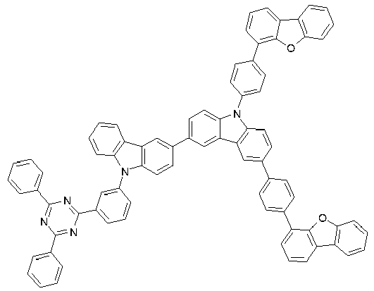
formule 28 formule 29 formule 30 


formule 37 formule 51 formule 75 


formule 79 formule 81 formule 82 

formule 83 formule 84 


formule 85 formule 86 formule 87 

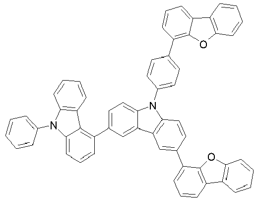
formule 88 formule 89 formule 140. - Composition comprenant au moins un composé selon l'une ou plusieurs parmi les revendications 1 à 9 et au moins un autre composé choisi dans le groupe constitué par les émetteurs fluorescents, les émetteurs phosphorescents, les matériaux hôtes, les matériaux matriciels, les matériaux de transport d'électrons, les matériaux d'injection d'électrons, les matériaux conducteurs de trous, les matériaux d'injection de trous, les matériaux de blocage d'électrons et les matériaux de blocage de trous.
- Formulation comprenant au moins un composé selon l'une ou plusieurs parmi les revendications 1 à 9 et/ou au moins une composition selon la revendication 10 et au moins un solvant.
- Utilisation d'un composé selon l'une ou plusieurs parmi les revendications 1 à 9 ou d'une composition selon la revendication 10, dans un dispositif électronique comme matériau de blocage de trous, matériau d'injection d'électrons et/ou matériau de transport d'électrons.
- Dispositif électronique comprenant au moins un composé selon l'une ou plusieurs parmi les revendications 1 à 9 ou une composition selon la revendication 10, le dispositif électronique étant choisi de préférence dans le groupe constitué par les dispositifs électroluminescents organiques, les circuits intégrés organiques, les transistors organiques à effet de champ, les transistors organiques en couches minces, les transistors organiques émetteurs de lumière, les cellules solaires organiques, les détecteurs optiques organiques, les photorécepteurs organiques, les dispositifs organiques à extinction de champ, les cellules électrochimiques émettrices de lumière et les diodes laser organiques.
- Utilisation d'un composé selon l'une ou plusieurs parmi les revendications 1 à 9, comme composant de systèmes à matrice mixte qui comprennent deux ou trois matériaux matriciels différents.
Applications Claiming Priority (2)
| Application Number | Priority Date | Filing Date | Title |
|---|---|---|---|
| EP14004391 | 2014-12-23 | ||
| PCT/EP2015/002360 WO2016102040A1 (fr) | 2014-12-23 | 2015-11-24 | Carbazoles comportant deux substituants dibenzofuranne ou dibenzothiophène |
Publications (2)
| Publication Number | Publication Date |
|---|---|
| EP3237409A1 EP3237409A1 (fr) | 2017-11-01 |
| EP3237409B1 true EP3237409B1 (fr) | 2022-01-05 |
Family
ID=52338787
Family Applications (1)
| Application Number | Title | Priority Date | Filing Date |
|---|---|---|---|
| EP15801678.2A Active EP3237409B1 (fr) | 2014-12-23 | 2015-11-24 | Carbazoles comportant deux substituants dibenzofuranne ou dibenzothiophène |
Country Status (7)
| Country | Link |
|---|---|
| US (1) | US10600970B2 (fr) |
| EP (1) | EP3237409B1 (fr) |
| JP (1) | JP6749913B2 (fr) |
| KR (1) | KR102572918B1 (fr) |
| CN (1) | CN107108589B (fr) |
| TW (1) | TWI707850B (fr) |
| WO (1) | WO2016102040A1 (fr) |
Families Citing this family (16)
| Publication number | Priority date | Publication date | Assignee | Title |
|---|---|---|---|---|
| KR102076884B1 (ko) * | 2015-12-08 | 2020-02-13 | 주식회사 엘지화학 | 헤테로고리 화합물 및 이를 포함하는 유기 발광 소자 |
| TWI766884B (zh) * | 2016-09-30 | 2022-06-11 | 德商麥克專利有限公司 | 具有二氮雜二苯并呋喃或二氮雜二苯并噻吩結構的化合物、其製法及其用途 |
| KR101865797B1 (ko) | 2017-01-03 | 2018-06-11 | 주식회사 엘지화학 | 변성 공액디엔계 중합체 및 이를 포함하는 고무 조성물 |
| DE102017102869A1 (de) | 2017-02-14 | 2018-08-16 | Cynora Gmbh | Organische Elektrolumineszenzvorrichtung |
| KR102794360B1 (ko) * | 2017-02-27 | 2025-04-14 | 삼성디스플레이 주식회사 | 유기 발광 소자 |
| US11296281B2 (en) * | 2017-03-15 | 2022-04-05 | Merck Patent Gmbh | Materials for organic electroluminescent devices |
| KR102121433B1 (ko) * | 2017-09-01 | 2020-06-10 | 주식회사 엘지화학 | 신규한 화합물 및 이를 이용한 유기발광 소자 |
| KR102407540B1 (ko) * | 2017-12-01 | 2022-06-10 | 엘지디스플레이 주식회사 | 유기 화합물과 이를 포함하는 유기발광다이오드 및 유기발광 표시장치 |
| CN109928961B (zh) * | 2017-12-15 | 2021-06-15 | 广东阿格蕾雅光电材料有限公司 | 含有4-硫砜芳基二苯并呋喃的光电材料及应用 |
| CN109928962A (zh) * | 2017-12-18 | 2019-06-25 | 江苏三月光电科技有限公司 | 一种以咔唑为核心的化合物、制备方法及其在有机电致发光器件上的应用 |
| CN112955437A (zh) * | 2018-11-05 | 2021-06-11 | 默克专利有限公司 | 可用于有机电子器件中的化合物 |
| JP7393345B2 (ja) * | 2018-12-14 | 2023-12-06 | 出光興産株式会社 | 有機エレクトロルミネッセンス素子、化合物、有機エレクトロルミネッセンス素子用材料、及び電子機器 |
| WO2020175624A1 (fr) * | 2019-02-27 | 2020-09-03 | 国立大学法人九州大学 | Composé, matériau électroluminescent et élément laser à semi-conducteur organique |
| CN112479978B (zh) * | 2019-09-11 | 2023-11-28 | 江苏三月科技股份有限公司 | 一种以咔唑衍生物为核心的有机化合物及其应用 |
| CN115960033B (zh) * | 2023-02-08 | 2024-05-07 | 东南大学 | 一种基于咔唑-苯腈的热活化延迟荧光树枝状异构体材料及其制备方法 |
| WO2025168515A1 (fr) | 2024-02-06 | 2025-08-14 | Merck Patent Gmbh | Matériaux pour dispositifs électroniques organiques |
Family Cites Families (13)
| Publication number | Priority date | Publication date | Assignee | Title |
|---|---|---|---|---|
| JP5359869B2 (ja) * | 2007-05-30 | 2013-12-04 | コニカミノルタ株式会社 | 有機エレクトロルミネッセンス素子、有機エレクトロルミネッセンス素子の製造方法、表示装置及び照明装置 |
| WO2009060757A1 (fr) * | 2007-11-08 | 2009-05-14 | Konica Minolta Holdings, Inc. | Dispositif électroluminescent organique, dispositif d'affichage et dispositif d'éclairage |
| JPWO2010044342A1 (ja) * | 2008-10-15 | 2012-03-15 | コニカミノルタホールディングス株式会社 | 有機エレクトロルミネッセンス素子、有機エレクトロルミネッセンス素子の製造方法、白色有機エレクトロルミネッセンス素子、表示装置及び照明装置 |
| JP5697856B2 (ja) | 2009-06-24 | 2015-04-08 | コニカミノルタ株式会社 | 有機エレクトロルミネッセンス素子、白色有機エレクトロルミネッセンス素子、表示装置及び照明装置 |
| EP2453496B1 (fr) * | 2009-07-07 | 2018-11-14 | Konica Minolta Holdings, Inc. | Élément électroluminescent organique, nouveau composé, dispositif d'éclairage et dispositif d'affichage |
| JP5604848B2 (ja) | 2009-10-19 | 2014-10-15 | コニカミノルタ株式会社 | 有機エレクトロルミネッセンス素子用材料、有機エレクトロルミネッセンス素子、照明装置及び表示装置 |
| KR101867115B1 (ko) * | 2010-12-28 | 2018-07-19 | 이데미쓰 고산 가부시키가이샤 | 유기 전기발광 소자용 재료 및 그것을 이용한 유기 전기발광 소자 |
| US8580399B2 (en) * | 2011-04-08 | 2013-11-12 | Universal Display Corporation | Substituted oligoazacarbazoles for light emitting diodes |
| EP2889296A4 (fr) | 2012-08-21 | 2016-06-15 | Cheil Ind Inc | Composé pour dispositif optoélectrique organique, diode électroluminescente organique le contenant et dispositif d'affichage contenant la diode électroluminescente organique |
| JP2014094935A (ja) * | 2012-10-10 | 2014-05-22 | Idemitsu Kosan Co Ltd | 化合物、及びそれを用いた有機エレクトロルミネッセンス素子 |
| KR101447961B1 (ko) * | 2013-02-01 | 2014-10-13 | (주)피엔에이치테크 | 새로운 유기전계발광소자용 화합물 및 그를 포함하는 유기전계발광소자 |
| KR101672074B1 (ko) * | 2013-05-07 | 2016-11-02 | 주식회사 엘지화학 | 헤테로환 화합물 및 이를 포함하는 유기 전자 소자 |
| KR101764976B1 (ko) * | 2014-09-18 | 2017-08-04 | 주식회사 엘지화학 | 헤테로고리 화합물 및 이를 포함하는 유기 발광 소자 |
-
2015
- 2015-11-24 WO PCT/EP2015/002360 patent/WO2016102040A1/fr not_active Ceased
- 2015-11-24 KR KR1020177020411A patent/KR102572918B1/ko active Active
- 2015-11-24 CN CN201580069711.7A patent/CN107108589B/zh active Active
- 2015-11-24 EP EP15801678.2A patent/EP3237409B1/fr active Active
- 2015-11-24 US US15/539,177 patent/US10600970B2/en active Active
- 2015-11-24 JP JP2017534332A patent/JP6749913B2/ja active Active
- 2015-12-21 TW TW104142957A patent/TWI707850B/zh not_active IP Right Cessation
Also Published As
| Publication number | Publication date |
|---|---|
| KR20170097189A (ko) | 2017-08-25 |
| TW201638087A (zh) | 2016-11-01 |
| US20190044071A1 (en) | 2019-02-07 |
| EP3237409A1 (fr) | 2017-11-01 |
| JP2018503622A (ja) | 2018-02-08 |
| US10600970B2 (en) | 2020-03-24 |
| CN107108589B (zh) | 2021-01-01 |
| JP6749913B2 (ja) | 2020-09-02 |
| WO2016102040A1 (fr) | 2016-06-30 |
| CN107108589A (zh) | 2017-08-29 |
| KR102572918B1 (ko) | 2023-08-30 |
| TWI707850B (zh) | 2020-10-21 |
Similar Documents
| Publication | Publication Date | Title |
|---|---|---|
| EP3519417B1 (fr) | Composés comprenant des structures diazadibenzofurane ou diazadibenzothiophène | |
| EP3237387B1 (fr) | Composés hétérocycliques à structures de dibenzazépine | |
| EP3519415B1 (fr) | Carbazoles comprenant des structures diazadibenzofurane ou diazadibenzothiophène | |
| EP3237409B1 (fr) | Carbazoles comportant deux substituants dibenzofuranne ou dibenzothiophène | |
| EP3708634B1 (fr) | Composés spiraniques hétérocycliques | |
| EP3052505B1 (fr) | Composés contenant du bore | |
| EP3221294B1 (fr) | Derives heterocycliques pour l'utilisation dans des dispositifs electroniques | |
| EP3016959B1 (fr) | Composés polycycliques | |
| EP3538623B1 (fr) | Composés pourvus d'un groupe accepteur et d'un groupe donneur | |
| EP3016952B1 (fr) | Composés de lactame spirocondensés pour des dispositifs électroluminescents organiques | |
| EP3548467B1 (fr) | Composés à structures valérolactame | |
| EP3328850B1 (fr) | Composés à structures fluorène | |
| EP3442968A1 (fr) | Composés hétérocycliques à structures dibenzofuranes et/ou dibenzothiophènes | |
| EP3430006A1 (fr) | Composés à structures spirobifluorène | |
| EP3856868B1 (fr) | Composés utilisables comme composés actifs dans un dispositif électronique organique | |
| EP3197887B1 (fr) | Composés hétérocycliques à structures benzo [c]coumarine | |
| WO2020064662A2 (fr) | Procédé de préparation de composés hétéroaromatiques azotés à encombrement stérique | |
| EP3548477B1 (fr) | Hétérocycles azotés destinés à être utilisés dans des diodes électroluminescentes organiques (oled) | |
| EP3512841B1 (fr) | Composés à structures spirobifluorène | |
| EP3548481B1 (fr) | Composés hétérocycliques à utiliser dans des dispositifs électroniques |
Legal Events
| Date | Code | Title | Description |
|---|---|---|---|
| STAA | Information on the status of an ep patent application or granted ep patent |
Free format text: STATUS: THE INTERNATIONAL PUBLICATION HAS BEEN MADE |
|
| PUAI | Public reference made under article 153(3) epc to a published international application that has entered the european phase |
Free format text: ORIGINAL CODE: 0009012 |
|
| STAA | Information on the status of an ep patent application or granted ep patent |
Free format text: STATUS: REQUEST FOR EXAMINATION WAS MADE |
|
| 17P | Request for examination filed |
Effective date: 20170531 |
|
| AK | Designated contracting states |
Kind code of ref document: A1 Designated state(s): AL AT BE BG CH CY CZ DE DK EE ES FI FR GB GR HR HU IE IS IT LI LT LU LV MC MK MT NL NO PL PT RO RS SE SI SK SM TR |
|
| AX | Request for extension of the european patent |
Extension state: BA ME |
|
| DAV | Request for validation of the european patent (deleted) | ||
| DAX | Request for extension of the european patent (deleted) | ||
| STAA | Information on the status of an ep patent application or granted ep patent |
Free format text: STATUS: EXAMINATION IS IN PROGRESS |
|
| 17Q | First examination report despatched |
Effective date: 20180713 |
|
| GRAP | Despatch of communication of intention to grant a patent |
Free format text: ORIGINAL CODE: EPIDOSNIGR1 |
|
| STAA | Information on the status of an ep patent application or granted ep patent |
Free format text: STATUS: GRANT OF PATENT IS INTENDED |
|
| INTG | Intention to grant announced |
Effective date: 20210913 |
|
| GRAS | Grant fee paid |
Free format text: ORIGINAL CODE: EPIDOSNIGR3 |
|
| GRAA | (expected) grant |
Free format text: ORIGINAL CODE: 0009210 |
|
| STAA | Information on the status of an ep patent application or granted ep patent |
Free format text: STATUS: THE PATENT HAS BEEN GRANTED |
|
| AK | Designated contracting states |
Kind code of ref document: B1 Designated state(s): AL AT BE BG CH CY CZ DE DK EE ES FI FR GB GR HR HU IE IS IT LI LT LU LV MC MK MT NL NO PL PT RO RS SE SI SK SM TR |
|
| REG | Reference to a national code |
Ref country code: GB Ref legal event code: FG4D Free format text: NOT ENGLISH |
|
| REG | Reference to a national code |
Ref country code: CH Ref legal event code: EP |
|
| REG | Reference to a national code |
Ref country code: AT Ref legal event code: REF Ref document number: 1460461 Country of ref document: AT Kind code of ref document: T Effective date: 20220115 |
|
| REG | Reference to a national code |
Ref country code: DE Ref legal event code: R096 Ref document number: 502015015563 Country of ref document: DE |
|
| REG | Reference to a national code |
Ref country code: IE Ref legal event code: FG4D Free format text: LANGUAGE OF EP DOCUMENT: GERMAN |
|
| REG | Reference to a national code |
Ref country code: LT Ref legal event code: MG9D |
|
| RAP4 | Party data changed (patent owner data changed or rights of a patent transferred) |
Owner name: MERCK PATENT GMBH |
|
| REG | Reference to a national code |
Ref country code: NL Ref legal event code: MP Effective date: 20220105 |
|
| PG25 | Lapsed in a contracting state [announced via postgrant information from national office to epo] |
Ref country code: NL Free format text: LAPSE BECAUSE OF FAILURE TO SUBMIT A TRANSLATION OF THE DESCRIPTION OR TO PAY THE FEE WITHIN THE PRESCRIBED TIME-LIMIT Effective date: 20220105 |
|
| PG25 | Lapsed in a contracting state [announced via postgrant information from national office to epo] |
Ref country code: SE Free format text: LAPSE BECAUSE OF FAILURE TO SUBMIT A TRANSLATION OF THE DESCRIPTION OR TO PAY THE FEE WITHIN THE PRESCRIBED TIME-LIMIT Effective date: 20220105 Ref country code: RS Free format text: LAPSE BECAUSE OF FAILURE TO SUBMIT A TRANSLATION OF THE DESCRIPTION OR TO PAY THE FEE WITHIN THE PRESCRIBED TIME-LIMIT Effective date: 20220105 Ref country code: PT Free format text: LAPSE BECAUSE OF FAILURE TO SUBMIT A TRANSLATION OF THE DESCRIPTION OR TO PAY THE FEE WITHIN THE PRESCRIBED TIME-LIMIT Effective date: 20220505 Ref country code: NO Free format text: LAPSE BECAUSE OF FAILURE TO SUBMIT A TRANSLATION OF THE DESCRIPTION OR TO PAY THE FEE WITHIN THE PRESCRIBED TIME-LIMIT Effective date: 20220405 Ref country code: LT Free format text: LAPSE BECAUSE OF FAILURE TO SUBMIT A TRANSLATION OF THE DESCRIPTION OR TO PAY THE FEE WITHIN THE PRESCRIBED TIME-LIMIT Effective date: 20220105 Ref country code: HR Free format text: LAPSE BECAUSE OF FAILURE TO SUBMIT A TRANSLATION OF THE DESCRIPTION OR TO PAY THE FEE WITHIN THE PRESCRIBED TIME-LIMIT Effective date: 20220105 Ref country code: ES Free format text: LAPSE BECAUSE OF FAILURE TO SUBMIT A TRANSLATION OF THE DESCRIPTION OR TO PAY THE FEE WITHIN THE PRESCRIBED TIME-LIMIT Effective date: 20220105 Ref country code: BG Free format text: LAPSE BECAUSE OF FAILURE TO SUBMIT A TRANSLATION OF THE DESCRIPTION OR TO PAY THE FEE WITHIN THE PRESCRIBED TIME-LIMIT Effective date: 20220405 |
|
| PG25 | Lapsed in a contracting state [announced via postgrant information from national office to epo] |
Ref country code: PL Free format text: LAPSE BECAUSE OF FAILURE TO SUBMIT A TRANSLATION OF THE DESCRIPTION OR TO PAY THE FEE WITHIN THE PRESCRIBED TIME-LIMIT Effective date: 20220105 Ref country code: LV Free format text: LAPSE BECAUSE OF FAILURE TO SUBMIT A TRANSLATION OF THE DESCRIPTION OR TO PAY THE FEE WITHIN THE PRESCRIBED TIME-LIMIT Effective date: 20220105 Ref country code: GR Free format text: LAPSE BECAUSE OF FAILURE TO SUBMIT A TRANSLATION OF THE DESCRIPTION OR TO PAY THE FEE WITHIN THE PRESCRIBED TIME-LIMIT Effective date: 20220406 Ref country code: FI Free format text: LAPSE BECAUSE OF FAILURE TO SUBMIT A TRANSLATION OF THE DESCRIPTION OR TO PAY THE FEE WITHIN THE PRESCRIBED TIME-LIMIT Effective date: 20220105 |
|
| PG25 | Lapsed in a contracting state [announced via postgrant information from national office to epo] |
Ref country code: IS Free format text: LAPSE BECAUSE OF FAILURE TO SUBMIT A TRANSLATION OF THE DESCRIPTION OR TO PAY THE FEE WITHIN THE PRESCRIBED TIME-LIMIT Effective date: 20220505 |
|
| REG | Reference to a national code |
Ref country code: DE Ref legal event code: R097 Ref document number: 502015015563 Country of ref document: DE |
|
| PG25 | Lapsed in a contracting state [announced via postgrant information from national office to epo] |
Ref country code: SM Free format text: LAPSE BECAUSE OF FAILURE TO SUBMIT A TRANSLATION OF THE DESCRIPTION OR TO PAY THE FEE WITHIN THE PRESCRIBED TIME-LIMIT Effective date: 20220105 Ref country code: SK Free format text: LAPSE BECAUSE OF FAILURE TO SUBMIT A TRANSLATION OF THE DESCRIPTION OR TO PAY THE FEE WITHIN THE PRESCRIBED TIME-LIMIT Effective date: 20220105 Ref country code: RO Free format text: LAPSE BECAUSE OF FAILURE TO SUBMIT A TRANSLATION OF THE DESCRIPTION OR TO PAY THE FEE WITHIN THE PRESCRIBED TIME-LIMIT Effective date: 20220105 Ref country code: EE Free format text: LAPSE BECAUSE OF FAILURE TO SUBMIT A TRANSLATION OF THE DESCRIPTION OR TO PAY THE FEE WITHIN THE PRESCRIBED TIME-LIMIT Effective date: 20220105 Ref country code: DK Free format text: LAPSE BECAUSE OF FAILURE TO SUBMIT A TRANSLATION OF THE DESCRIPTION OR TO PAY THE FEE WITHIN THE PRESCRIBED TIME-LIMIT Effective date: 20220105 Ref country code: CZ Free format text: LAPSE BECAUSE OF FAILURE TO SUBMIT A TRANSLATION OF THE DESCRIPTION OR TO PAY THE FEE WITHIN THE PRESCRIBED TIME-LIMIT Effective date: 20220105 |
|
| PLBE | No opposition filed within time limit |
Free format text: ORIGINAL CODE: 0009261 |
|
| STAA | Information on the status of an ep patent application or granted ep patent |
Free format text: STATUS: NO OPPOSITION FILED WITHIN TIME LIMIT |
|
| PG25 | Lapsed in a contracting state [announced via postgrant information from national office to epo] |
Ref country code: AL Free format text: LAPSE BECAUSE OF FAILURE TO SUBMIT A TRANSLATION OF THE DESCRIPTION OR TO PAY THE FEE WITHIN THE PRESCRIBED TIME-LIMIT Effective date: 20220105 |
|
| 26N | No opposition filed |
Effective date: 20221006 |
|
| PG25 | Lapsed in a contracting state [announced via postgrant information from national office to epo] |
Ref country code: SI Free format text: LAPSE BECAUSE OF FAILURE TO SUBMIT A TRANSLATION OF THE DESCRIPTION OR TO PAY THE FEE WITHIN THE PRESCRIBED TIME-LIMIT Effective date: 20220105 |
|
| P01 | Opt-out of the competence of the unified patent court (upc) registered |
Effective date: 20230518 |
|
| PG25 | Lapsed in a contracting state [announced via postgrant information from national office to epo] |
Ref country code: MC Free format text: LAPSE BECAUSE OF FAILURE TO SUBMIT A TRANSLATION OF THE DESCRIPTION OR TO PAY THE FEE WITHIN THE PRESCRIBED TIME-LIMIT Effective date: 20220105 |
|
| REG | Reference to a national code |
Ref country code: CH Ref legal event code: PL |
|
| GBPC | Gb: european patent ceased through non-payment of renewal fee |
Effective date: 20221124 |
|
| REG | Reference to a national code |
Ref country code: BE Ref legal event code: MM Effective date: 20221130 |
|
| PG25 | Lapsed in a contracting state [announced via postgrant information from national office to epo] |
Ref country code: LI Free format text: LAPSE BECAUSE OF NON-PAYMENT OF DUE FEES Effective date: 20221130 Ref country code: IT Free format text: LAPSE BECAUSE OF FAILURE TO SUBMIT A TRANSLATION OF THE DESCRIPTION OR TO PAY THE FEE WITHIN THE PRESCRIBED TIME-LIMIT Effective date: 20220105 Ref country code: CH Free format text: LAPSE BECAUSE OF NON-PAYMENT OF DUE FEES Effective date: 20221130 |
|
| PG25 | Lapsed in a contracting state [announced via postgrant information from national office to epo] |
Ref country code: LU Free format text: LAPSE BECAUSE OF NON-PAYMENT OF DUE FEES Effective date: 20221124 |
|
| PG25 | Lapsed in a contracting state [announced via postgrant information from national office to epo] |
Ref country code: IE Free format text: LAPSE BECAUSE OF NON-PAYMENT OF DUE FEES Effective date: 20221124 Ref country code: GB Free format text: LAPSE BECAUSE OF NON-PAYMENT OF DUE FEES Effective date: 20221124 |
|
| PG25 | Lapsed in a contracting state [announced via postgrant information from national office to epo] |
Ref country code: FR Free format text: LAPSE BECAUSE OF NON-PAYMENT OF DUE FEES Effective date: 20221130 Ref country code: BE Free format text: LAPSE BECAUSE OF NON-PAYMENT OF DUE FEES Effective date: 20221130 |
|
| REG | Reference to a national code |
Ref country code: AT Ref legal event code: MM01 Ref document number: 1460461 Country of ref document: AT Kind code of ref document: T Effective date: 20221124 |
|
| PG25 | Lapsed in a contracting state [announced via postgrant information from national office to epo] |
Ref country code: AT Free format text: LAPSE BECAUSE OF NON-PAYMENT OF DUE FEES Effective date: 20221124 |
|
| PG25 | Lapsed in a contracting state [announced via postgrant information from national office to epo] |
Ref country code: HU Free format text: LAPSE BECAUSE OF FAILURE TO SUBMIT A TRANSLATION OF THE DESCRIPTION OR TO PAY THE FEE WITHIN THE PRESCRIBED TIME-LIMIT; INVALID AB INITIO Effective date: 20151124 |
|
| PG25 | Lapsed in a contracting state [announced via postgrant information from national office to epo] |
Ref country code: CY Free format text: LAPSE BECAUSE OF FAILURE TO SUBMIT A TRANSLATION OF THE DESCRIPTION OR TO PAY THE FEE WITHIN THE PRESCRIBED TIME-LIMIT Effective date: 20220105 |
|
| PG25 | Lapsed in a contracting state [announced via postgrant information from national office to epo] |
Ref country code: MK Free format text: LAPSE BECAUSE OF FAILURE TO SUBMIT A TRANSLATION OF THE DESCRIPTION OR TO PAY THE FEE WITHIN THE PRESCRIBED TIME-LIMIT Effective date: 20220105 |
|
| PG25 | Lapsed in a contracting state [announced via postgrant information from national office to epo] |
Ref country code: MT Free format text: LAPSE BECAUSE OF FAILURE TO SUBMIT A TRANSLATION OF THE DESCRIPTION OR TO PAY THE FEE WITHIN THE PRESCRIBED TIME-LIMIT Effective date: 20220105 |
|
| PG25 | Lapsed in a contracting state [announced via postgrant information from national office to epo] |
Ref country code: TR Free format text: LAPSE BECAUSE OF FAILURE TO SUBMIT A TRANSLATION OF THE DESCRIPTION OR TO PAY THE FEE WITHIN THE PRESCRIBED TIME-LIMIT Effective date: 20220105 |
|
| PGFP | Annual fee paid to national office [announced via postgrant information from national office to epo] |
Ref country code: DE Payment date: 20251022 Year of fee payment: 11 |