EP3237995B1 - Protection de courant maximal de système - Google Patents
Protection de courant maximal de système Download PDFInfo
- Publication number
- EP3237995B1 EP3237995B1 EP15873904.5A EP15873904A EP3237995B1 EP 3237995 B1 EP3237995 B1 EP 3237995B1 EP 15873904 A EP15873904 A EP 15873904A EP 3237995 B1 EP3237995 B1 EP 3237995B1
- Authority
- EP
- European Patent Office
- Prior art keywords
- domains
- domain
- current
- frequency
- expected
- Prior art date
- Legal status (The legal status is an assumption and is not a legal conclusion. Google has not performed a legal analysis and makes no representation as to the accuracy of the status listed.)
- Not-in-force
Links
Images


Classifications
-
- G—PHYSICS
- G06—COMPUTING OR CALCULATING; COUNTING
- G06F—ELECTRIC DIGITAL DATA PROCESSING
- G06F1/00—Details not covered by groups G06F3/00 - G06F13/00 and G06F21/00
- G06F1/26—Power supply means, e.g. regulation thereof
- G06F1/32—Means for saving power
- G06F1/3203—Power management, i.e. event-based initiation of a power-saving mode
- G06F1/3234—Power saving characterised by the action undertaken
- G06F1/324—Power saving characterised by the action undertaken by lowering clock frequency
-
- G—PHYSICS
- G05—CONTROLLING; REGULATING
- G05F—SYSTEMS FOR REGULATING ELECTRIC OR MAGNETIC VARIABLES
- G05F1/00—Automatic systems in which deviations of an electric quantity from one or more predetermined values are detected at the output of the system and fed back to a device within the system to restore the detected quantity to its predetermined value or values, i.e. retroactive systems
- G05F1/10—Regulating voltage or current
-
- G—PHYSICS
- G06—COMPUTING OR CALCULATING; COUNTING
- G06F—ELECTRIC DIGITAL DATA PROCESSING
- G06F1/00—Details not covered by groups G06F3/00 - G06F13/00 and G06F21/00
- G06F1/26—Power supply means, e.g. regulation thereof
- G06F1/28—Supervision thereof, e.g. detecting power-supply failure by out of limits supervision
-
- G—PHYSICS
- G06—COMPUTING OR CALCULATING; COUNTING
- G06F—ELECTRIC DIGITAL DATA PROCESSING
- G06F1/00—Details not covered by groups G06F3/00 - G06F13/00 and G06F21/00
- G06F1/26—Power supply means, e.g. regulation thereof
- G06F1/32—Means for saving power
- G06F1/3203—Power management, i.e. event-based initiation of a power-saving mode
- G06F1/3206—Monitoring of events, devices or parameters that trigger a change in power modality
-
- H—ELECTRICITY
- H03—ELECTRONIC CIRCUITRY
- H03K—PULSE TECHNIQUE
- H03K7/00—Modulating pulses with a continuously-variable modulating signal
- H03K7/08—Duration or width modulation ; Duty cycle modulation
-
- H—ELECTRICITY
- H03—ELECTRONIC CIRCUITRY
- H03L—AUTOMATIC CONTROL, STARTING, SYNCHRONISATION OR STABILISATION OF GENERATORS OF ELECTRONIC OSCILLATIONS OR PULSES
- H03L7/00—Automatic control of frequency or phase; Synchronisation
- H03L7/06—Automatic control of frequency or phase; Synchronisation using a reference signal applied to a frequency- or phase-locked loop
- H03L7/08—Details of the phase-locked loop
-
- Y—GENERAL TAGGING OF NEW TECHNOLOGICAL DEVELOPMENTS; GENERAL TAGGING OF CROSS-SECTIONAL TECHNOLOGIES SPANNING OVER SEVERAL SECTIONS OF THE IPC; TECHNICAL SUBJECTS COVERED BY FORMER USPC CROSS-REFERENCE ART COLLECTIONS [XRACs] AND DIGESTS
- Y02—TECHNOLOGIES OR APPLICATIONS FOR MITIGATION OR ADAPTATION AGAINST CLIMATE CHANGE
- Y02D—CLIMATE CHANGE MITIGATION TECHNOLOGIES IN INFORMATION AND COMMUNICATION TECHNOLOGIES [ICT], I.E. INFORMATION AND COMMUNICATION TECHNOLOGIES AIMING AT THE REDUCTION OF THEIR OWN ENERGY USE
- Y02D10/00—Energy efficient computing, e.g. low power processors, power management or thermal management
Definitions
- Embodiments of the present invention relate to the field of power management; more particularly, embodiments of the present invention relate to determining whether expected current for a device (e.g., system-on-a-chip (SOC)) is within the current for the device.
- a device e.g., system-on-a-chip (SOC)
- High performance SoCs are subject to a series of power delivery network (PDN) limitations.
- PDN power delivery network
- One such limitation involves small batteries and their potential for becoming stressed into failure by short bursts of high power consumption from a process running on an SoC. If the instantaneous power being consumed by the SoC is able to exceed a set limit, the instantaneous power may significantly impact the power supply and battery. Also, exceeding this limit can result in an I*R voltage drop that can result with "bluescreen" or trigger overcurrent protection and shut down the system. Thus, the instantaneous current can pose a significant limitation on the system.
- PL1 is the long-term CPU power limit that the system can withstand without overheating.
- PL2 is the short-term burst limit used for temporary excursions to higher clocks (e.g., a quick trip to a faster clock frequency to improve responsiveness while loading a program).
- PL3 is dynamic voltage and frequency scaling technique used on a chip. PL2 is measured in seconds, while the PL3 limit is monitored in milliseconds to prevent instantaneous power use from damaging a device's battery.
- an interface on the platform level monitors when the instantaneous power limit is surpassed and sends a signal, from the platform, to the central processing unit (CPU) to throttle its operation and bring the current down below the instantaneous limit.
- CPU central processing unit
- US 2011/0291746 discloses an integrated circuit comprising a power management module for adapting power consumption of the integrated circuit based on a comparison of the runtime power consumption estimate with one or more predetermined thresholds.
- a method and apparatus to limit the power of an integrated circuit is disclosed.
- the IC may be a system-on-a-chip (SoC), a processor, etc.
- SoC system-on-a-chip
- the power limit process performs proactive calculations and maintains the total IC instantaneous power below the power limit.
- the power calculation is done proactively before making a transition to a new state for the IC (e.g., a new working point).
- the expected current for each domain e.g., a voltage regulator (VR) domain
- VR voltage regulator
- the expected current for each domain is calculated and multiplied by a target voltage for that new state to create a sum representing the expected power for that domain when in the new state.
- the expected current for each domain is calculated based on leakage, maximum power vs. dynamic capacitance (C dyn ) and target frequency to be used in the new state. All of the expected power values for the various domains are added together to create a total expected power, which is compared to the power limit. If the total expected power is greater than the limit, then the frequency of one or more of the domains is reduced so that the total power of the new state (e.g., the new working point) would be below the power limit.
- C dyn maximum power vs. dynamic capacitance
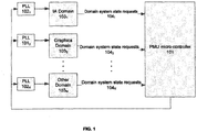
- FIG. 1 is a block diagram of one embodiment of an integrated circuit (IC).
- the integrated circuit includes a number of domains.
- instruction architecture (IA) domain 103 1 e.g., a central processing unit (CPU) domain
- graphics domain 103 2 e.g., a graphics domain
- domain 103 N e.g., a graphics domain
- Each domain may have one or more cores (e.g., processor core, execution core) or special purpose logic.
- Power Management Unit (PMU) microcontroller 101 controls and manages power for the IC.
- PMU microcontroller 101 specifies a frequency of a clock for each of the domains.
- PMU microcontroller 101 signals each of those frequencies to phase locked loops (PLLs) associated with each of the domains.
- the PLLs include PLL 102 1 which provides clock for IA domain 103 1 , PLL 102 2 which provides the clock to graphics domain 103 2 , and PLL 104 N which provides a clock for domain 103 N .
- PMU microcontroller 101 is part of a CPU.
- each of domains 103 provides a domain specific system state request to PMU microcontroller 101.
- IA domain 103 1 , graphics domain 103 2 and other domain 103 N provide domain specific system state requests 104 1 , 104 2 , 104 N to PMU microcontroller 101.
- the specific system state requests specifies the state that the particular domain is going to be in after a transition.
- the system state request includes a frequency and at least one of a sleep state or an execution state. Note that sleep state and execution states for processor cores and domains associated with processor cores are well known in the art.
- PMU microcontroller 101 Based on the received domain system state requests, PMU microcontroller 101 generates calculates, for each domain, the expected current associated with the system state it will be in after the transition as well as the expected power associated with the domain in that system state. In other words, before every change in system state, PMU microcontroller 101 calculates expected current for each domain at the new working point. Note that after each transition, some domains may be in the same or a different system state, and therefore, the expected power calculations for one or more of the domains may be equal to their current power usage.
- this power limit is an instantaneous power limit.
- the power limit is set any an external agent (e.g., BIOS, an embedded controller, etc.).
- the power limit is set by control software. In such a case, the control software sets either statically or at runtime.
- PMU microcontroller 101 does nothing and allows the transition into the system state. If the sum does exceed the power limit, PMU microcontroller 101 takes one or more actions to lower the expected power that results from the transition. In one embodiment, one of the actions performed by PMU microcontroller 101 when the sum exceeds the power limit is to reduce the frequency of the system state for each of the domains. PMU microcontroller 101 then signals the reduced frequency to the corresponding clock generator (e.g., PLL) for use in generating a clock for its domain. In this manner, PMU microcontroller 101 performs domain frequency control.
- the corresponding clock generator e.g., PLL
- PMU microcontroller 101 calculates both the active and static current that is expected to exist for the domain when is in the new system state it requested. In one embodiment, PMU microcontroller 101 calculates the active current by summing the worst case C dyn for over all waking cores (i.e., cores that are not in idle or otherwise in powered down (e.g., gated) state). The worst case C dyn varies according to the execution state of the domain. PMU microcontroller 101 multiplies the worst case C dyn by the frequency and voltage associated with the requested system state. In one embodiment, the frequency is specified in the requested system state information, while the voltage is determined by the PMU microcontroller 101 as a function of the frequency.
- PMU microcontroller 101 also determines the static current of the domain.
- the static current is determined by taking the estimated leakage at that voltage of the domain in the requested state and the current temperature (as measured with temperature sensors). PMU microcontroller 101 sums the estimated leakage over all leaking cores in the domain, and gated cores are not counted. Note that the base core leakage can vary according to internal gating.
- PMU microcontroller 101 sums the active current and static current together. This represents the worst case current for a domain.
- the current for the domain in the requested system state may be based on previously measured currents, where a maximum current is identified over time. This maximum current would then be used as the worst case current for the domain.
- PMU microcontroller 101 multiplies this worst case current per domain by its voltage for the requested system state (at the specified frequency) to get the calculated worst case power for the domain. PMU microcontroller 101 sums the calculated worst case powers for all of the domains to obtain the calculated worst case power for the IC taking into account the system states requested by all the domains.
- PMU microcontroller 101 compares the total calculated worst case (expected) power with a power limit. If the calculated power is below the power limit, no action is taken and the transition to the requested system states by each of the domains occurs. If the calculated power is above the power limit, then PMU microcontroller 101 takes one or more actions, such as reducing the frequencies that the domains will use in the new system state by a factor. In one embodiment, this factor is the ratio between the power limit and the calculated power: power limit/calculated worst case power.
- PMU microcontroller 101 lowers the requested frequency of each domain by the ratio. That is, the reduction is done by calculating the ratio and multiplying it by each of the frequencies. In one embodiment, if the result of the multiplication is not a round number, the reduced frequencies are rounded down. This should ensure that the power usage associated with new system state, or working point, is below the power limit. If not, the process is repeated again.
- the ratio is only applied to a subset of domains.
- one or more additional power reduction actions may need to be performed to bring the expected power under the power limit.
- frequencies in the SoC system agent (SA) domain are not throttled. These include frequencies of the memory clock.
- extra throttling has to be done to the other domains, such as the instruction architecture (IA) domain to compensate.
- the new frequency for each domain is selected in an alternative manner.
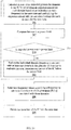
- FIG. 2A is a flow diagram of one embodiment of a process for performing a system state transition.
- the process is performed by processing logic that may comprise hardware (circuitry, dedicated logic, etc.), software (such as is run on a general purpose computer system or a dedicated machine), firmware, or a combination of these three.
- processing logic calculates a sum of the expected powers for domains in the IC by calculating an expected current for each of the plurality of domains based on an individual domain frequency in the new state and multiplying the expected current with its associated voltage for each of the plurality of domains for the new state (processing block 201).
- calculating the expected current for each domain is based on current leakage, target frequency, and dynamic capacitance (C dyn ).
- the new state includes a frequency and one or more of a sleep state and execution state for each domain.
- calculating the expected current for each domain comprises calculating active and static current for each domain and then summing the two together.
- Figure 2B is a flow diagram of one embodiment for calculating the expected current for each domain.
- the process is performed by processing logic that may comprise hardware (circuitry, dedicated logic, etc.), software (such as is run on a general purpose computer system or a dedicated machine), firmware, or a combination of these three.
- the process includes calculating the active current for the domain, including summing worst case C dyn for each core in the domain that is in a waking state and multiplying the worst case C dyn by the frequency and the associated voltage for the domain (processing block 211).
- the associated voltage is a function of the requested frequency.
- processing logic also calculates the static current by summing the leakage current for each core in the domain (processing block 212). These are cores that are in a waking state, and not in an idle or powered down (e.g., power gated) state.
- the leakage current is the estimated leakage current at the voltage and temperature of the core (domain).
- processing logic compares the sum to a power limit (processing block 202). Next, processing logic tests whether the sum of the expected power for the domains is greater than the power limit (processing block 210). If the sum is greater than the power limit, then processing logic transitions to processing block 203 where processing logic reduces the frequency associated with at least one domain (e.g., more than one domain, all domains) in the plurality of domains to maintain the total instantaneous power of the IC below the power limit and the process transitions to processing block 201 where the process repeats.
- processing logic reduces the frequency associated with at least one domain (e.g., more than one domain, all domains) in the plurality of domains to maintain the total instantaneous power of the IC below the power limit and the process transitions to processing block 201 where the process repeats.
- reducing the individual domain frequency associated with each domain in the plurality of domains comprises calculating a ratio between the total of the expected worst case power for the domains and the power limit and reducing the individual domain frequency associated with each domain in the plurality of domains by at least the ratio.
- processing logic also sends a notification to indicate that the sum is greater than the power limit.
- the notification is sent to software (e.g., the operating system, BIOS, etc.).
- the notification is made by setting a status bit in a memory on the IC (e.g., a machine state register (MSR), memory-mapped input/output (MMIO) register.
- the notification is made through the use of an interrupt.
- processing logic sends new frequency values specifying a frequency to use in each domain to clock generators (PLLs) associated with those domains.
- processing logic permits the transition into the new state (processing block 205).
- Figure 3 is a flow diagram of one embodiment of a process for determining whether to perform a system state transition.
- the process is performed by processing logic that may comprise hardware (circuitry, dedicated logic, etc.), software (such as is run on a general purpose computer system or a dedicated machine), firmware, or a combination of these three.
- the process is performed by a power management unit in a device (e.g., a SoC, a processor, etc.).
- processing logic tests whether the power 301 associated with a new system state (sum of expected power for the domains) is greater than the power limit 302 associated with the power limit for the platform (processing block 310). If it is not, processing logic transitions to processing block 340 where processing logic performs the transition to the new system state. However, if the power 301 associated with the new system state is greater than power limit 302, the processor transitions to processing block 320 where processing logic lowers the frequencies.
- the reduction is done by calculating a ratio and multiplying it by each of the frequencies that have been requested by each of the domains. In one embodiment, the ratio is the power limit divided by total expected power of the domains. Each of the frequencies requested for the new system state is multiplied with the ration to create the frequency that will be used in the new system state. In one embodiment, any necessary rounding of the newly calculated frequency values is performed by rounding down the values.
- processing logic calculates a new work point (processing block 320) and transitions to processing block 310 to repeat the process.
- Figure 4 is a flow diagram of one embodiment of the process for summing the power for all the domains.
- the process is performed by processing logic that may comprise hardware (circuitry, dedicated logic, etc.), software (such as is run on a general purpose computer system or a dedicated machine), firmware, or a combination of these three.
- the process is performed by a power management unit in a device (e.g., a SoC, a processor, etc.).
- a per domain power calculation based on the expected power in their new state after the transition is performed for each of the domains, such as domain IA 401, domain graphics 402, domain SA 403 and other domain 404.
- the device may have more or less domains for which a separate per domain power calculation are performed.
- the expected power calculation for each of the domains are summed by summing logic 405 to generate the calculated power.
- the calculated power 410 is an input to the PMU logic to determine whether the system can transition to a new system state.
- Figure 5 is a flow diagram of one embodiment of a process for performing a per domain power calculation.
- the process is performed by processing logic that may comprise hardware (circuitry, dedicated logic, etc.), software (such as is run on a general purpose computer system or a dedicated machine), firmware, or a combination of these three.
- the process is performed by a power management unit in a device (e.g., a SoC, a processor, etc.).
- Logic 510 for calculating the current and voltage for the current domain receives an input frequency 501 along with system state inputs 502.
- Frequency 501 represents the frequency the domain requests to use when in the new system state.
- the core state inputs represent the new system states of different cores in the domain. As shown, there are state inputs for cores 0-N. Note that some domains may only have one core, while other domains have two or more cores. In case of a multi-core domain, all cores are clocked at the same frequency, though this is not required for teachings described herein.
- Domain current calculator 520 sends frequency 501 to logic 520 which generates a voltage 503 associated with the new state based on frequency 501.
- a frequency-voltage curve is used to assign each frequency a matching voltage.
- logic 520 includes a table that specifies a particular voltage associated with each frequency to which is provided. The logic 510 uses these inputs to determine the expected current that would be associated with the new state.
- Logic 510 outputs expected current 504 along with voltage 503 to power calculation unit 530.
- Power calculation unit 530 multiplies expected current 504 with voltage 503 to generate power 505, which represents the worst case power that the domain in the new state.
- Figure 6 is a flow diagram of one embodiment of a process for performing the platform power calculation.
- the process is performed by processing logic that may comprise hardware (circuitry, dedicated logic, etc.), software (such as is run on a general purpose computer system or a dedicated machine), firmware, or a combination of these three.
- the process is performed by a power management unit in a device (e.g., a SoC, a processor, etc.).
- Processing logic receives a configuration change indication 601.
- indication 601 relates to a battery drain situation. As the battery drains, it can sustain lower power draws, voltage drops as the battery drains. A sudden power drain can cause a sudden voltage drop, and if the battery is drained, it can sustain lower power drain before it goes below a voltage threshold. To avoid this, software sets a limit according to battery drain, triggering a change in the indication. This enables to extend battery life.
- Figure 7 is a block diagram of a processor 700 that may have more than one core, may have an integrated memory controller, and may have integrated graphics according to embodiments of the invention.
- the solid lined boxes in Figure 7 illustrate a processor 700 with a single core 702A, a system agent 710, a set of one or more bus controller units 716, while the optional addition of the dashed lined boxes illustrates an alternative processor 700 with multiple cores 702A-N, a set of one or more integrated memory controller unit(s) 714 in the system agent unit 710, and special purpose logic 708.
- different implementations of the processor 700 may include: 1) a CPU with the special purpose logic 708 being integrated graphics and/or scientific (throughput) logic (which may include one or more cores), and the cores 702A-N being one or more general purpose cores (e.g., general purpose in-order cores, general purpose out-of-order cores, a combination of the two); 2) a coprocessor with the cores 702A-N being a large number of special purpose cores intended primarily for graphics and/or scientific (throughput); and 3) a coprocessor with the cores 702A-N being a large number of general purpose in-order cores.
- the special purpose logic 708 being integrated graphics and/or scientific (throughput) logic
- the cores 702A-N being one or more general purpose cores (e.g., general purpose in-order cores, general purpose out-of-order cores, a combination of the two)
- a coprocessor with the cores 702A-N being a large number of special purpose core
- the processor 700 may be a general-purpose processor, coprocessor or special-purpose processor, such as, for example, a network or communication processor, compression engine, graphics processor, GPGPU (general purpose graphics processing unit), a high-throughput many integrated core (MIC) coprocessor (including 30 or more cores), embedded processor, or the like.
- the processor may be implemented on one or more chips.
- the processor 700 may be a part of and/or may be implemented on one or more substrates using any of a number of process technologies, such as, for example, BiCMOS, CMOS, or NMOS.
- each of the cores described above represents a different power domain that has a separate clock generator (e.g., PLL) and a voltage regulator.
- PLL clock generator
- another portion of special purpose logic 708 comprises a power management unit (PMU) such as the PMU described above.
- PMU power management unit
- the memory hierarchy includes one or more levels of cache within the cores, a set or one or more shared cache units 706, and external memory (not shown) coupled to the set of integrated memory controller units 714.
- the set of shared cache units 706 may include one or more mid-level caches, such as level 2 (L2), level 3 (L3), level 4 (L4), or other levels of cache, a last level cache (LLC), and/or combinations thereof. While in one embodiment a ring based interconnect unit 712 interconnects the special purpose logic 708, the set of shared cache units 706, and the system agent unit 710/integrated memory controller unit(s) 714, alternative embodiments may use any number of well-known techniques for interconnecting such units. In one embodiment, coherency is maintained between one or more cache units 706 and cores 702AN.
- the system agent 710 includes those components coordinating and operating cores 702A-N.
- the system agent unit 710 may include for example a power control unit (PCU) and a display unit.
- the PCU may be or include logic and components needed for regulating the power state of the cores 702A-N and the integrated graphics logic 708.
- the display unit is for driving one or more externally connected displays.
- the cores 702A-N may be homogenous or heterogeneous in terms of architecture instruction set; that is, two or more of the cores 702A-N may be capable of execution the same instruction set, while others may be capable of executing only a subset of that instruction set or a different instruction set.
- FIG. 8 is a block diagram of a SoC 800 in accordance with an embodiment of the present invention. Similar elements in Figure 7 bear like reference numerals. Also, dashed lined boxes are optional features on more advanced SoCs.
- an interconnect unit(s) 802 is coupled to: an application processor 810 which includes a set of one or more cores 202A-N and shared cache unit(s) 706; a system agent unit 710; a bus controller unit(s) 716; an integrated memory controller unit(s) 714; a set or one or more coprocessors 820 which may include integrated graphics logic, an image processor, an audio processor, and a video processor; an static random access memory (SRAM) unit 830; a direct memory access (DMA) unit 832; and a display unit 840 for coupling to one or more external displays.
- the coprocessor(s) 820 include a special-purpose processor, such as, for example, a network or communication processor, compression engine, GPGPU, a high-through
- a method comprises: prior to transitioning to a new state for an integrated circuit (IC), calculating a sum of expected powers for a plurality of domains in the IC by calculating an expected current for each of the plurality of domains based on an individual domain frequency in the new state and multiplying the expected current with its associated voltage for each of the plurality of domains for the new state; comparing the sum to a power limit; and if the sum is greater than the power limit, then reducing the individual domain frequency associated with at least one domain in the plurality of domains to maintain the total instantaneous power of the IC below the power limit.
- IC integrated circuit
- the subject matter of the first example embodiment can optionally include that calculating the expected current for each of the plurality of domains is based on current leakage, target frequency, and dynamic capacitance (C dyn ).
- the subject matter of the first example embodiment can optionally include that calculating the expected current for each of the plurality of domains comprises calculating active and static current and summing the active and static current.
- the subject matter of the this example embodiment can optionally include that calculating active current comprises summing worst case C dyn for each core in the domain that is in a waking state and multiplying the worst case C dyn by the frequency and the associated voltage for the domain.
- the subject matter of this example embodiment can optionally include that the associated voltage is a function of the requested frequency.
- the subject matter of the first example embodiment can optionally include that calculating static current comprises summing leakage for each core in the domain in the waking state.
- the subject matter of this example embodiment can optionally include that the leakage is the estimated leakage at the voltage and temperature of the domain.
- the subject matter of the first example embodiment can optionally include that reducing the individual domain frequency associated with at least one domain in the plurality of domains comprises calculating a ratio between the sum of the power and the power limit and reducing the individual domain frequency associated with each domain in the plurality of domains by at least the ratio.
- the subject matter of the first example embodiment can optionally include sending new frequency values specifying a frequency to use in each of the plurality of domains to clock generators (PLLs) associated with each of the plurality of domains.
- PLLs clock generators
- the subject matter of the first example embodiment can optionally include that if the sum is less than the power limit, then transitioning the IC into the new state.
- the subject matter of the first example embodiment can optionally include that the new state includes a frequency and one or more of a sleep state and execution state for each of the plurality of domains.
- the subject matter of the first example embodiment can optionally include sending a notification in response to determining the sum is higher than the power limit.
- the subject matter of the first example embodiment can optionally include determining the power limit by: determining available power based on one or more of alternating current adapter capability and charge state of a battery, if any; calculating a maximum power capability for the IC; calculating a maximum power for a portion of the IC that is not included in the plurality of domains; and setting the power limit as the difference between maximum power capability for the IC and the maximum power capability for the portion of the IC that is not included in the plurality of domains.
- an integrated circuit comprises: a plurality of domains; and a unit coupled to the domains to, in response to receiving a request from each domain in the plurality of domains, calculate a sum of expected powers for the plurality of domains by calculating an expected current for each of the plurality of domains based on an individual domain frequency in a new state and multiplying the expected current with its associated voltage for each of the plurality of domains for the new state, prior to transitioning to the new state, compare the sum to a power limit, and if the sum is greater than the power limit, then reduce the individual domain frequency associated with at least one domain in the plurality of domains to maintain the total instantaneous power of the IC below the power limit.
- the subject matter of the second example embodiment can optionally include that the unit calculates the expected current for each of the plurality of domains based on current leakage, target frequency, and dynamic capacitance (C dyn ).
- the subject matter of the second example embodiment can optionally include that the unit the expected current for each of the plurality of domains by calculating active and static current and summing the active and static current.
- the subject matter of the second example embodiment can optionally include that the unit calculates active current by summing worst case C dyn for each core in the domain that is in a waking state and multiplying the worst case C dyn by the frequency and the associated voltage for the domain.
- the subject matter of the second example embodiment can optionally include that the associated voltage is a function of the requested frequency.
- the subject matter of the second example embodiment can optionally include that the unit calculates static current by summing leakage for each core in the domain in a waking state (e.g., a non-powered down state).
- a waking state e.g., a non-powered down state
- the subject matter of the second example embodiment can optionally include that the leakage is the estimated leakage at the voltage and temperature of the domain.
- the subject matter of the second example embodiment can optionally include that the unit reduces the individual domain frequency associated with at least one domain in the plurality of domains by calculating a ratio between the sum of the power and the power limit and reducing the individual domain frequency associated with each domain in the plurality of domains by at least the ratio.
- the subject matter of the second example embodiment can optionally include that the unit sends new frequency values specifying a frequency to use in each of the plurality of domains to clock generators (PLLs) associated with each of the plurality of domains.
- PLLs clock generators
- the subject matter of the second example embodiment can optionally include that if the sum is less than the power limit, then the IC transitions into the new state.
- the subject matter of the second example embodiment can optionally include that the new state includes a frequency and one or more of a sleep state and execution state for each of the plurality of domains.
- a method comprises: generating a new frequency for each of a plurality of domains in an integrated circuit (IC) based on a comparison between a power limit for the IC and a worst case power calculation derived from a worst case current determination associated with a state said each domain requests to enter; and signaling clock generators (PLLs) associated with each of the plurality of domains the new frequency of a clock to generate for use in each of the plurality of domains to clock generators (PLLs) associated with each of the plurality of domains.
- PLLs clock generators
- the subject matter of the third example embodiment can optionally include that the worst case current determination comprises is based on a calculation of the expected current for each of the plurality of domains based on current leakage, target frequency, and dynamic capacitance (C dyn ).
- an article of manufacture has one or more non-transitory computer readable media storing instructions which when executed causes an integrated circuit to perform a method comprising: prior to transitioning to a new state for an integrated circuit (IC), calculating a sum of expected powers for a plurality of domains in the IC by calculating an expected current for each of the plurality of domains based on an individual domain frequency in the new state and multiplying the expected current with its associated voltage for each of the plurality of domains for the new state; comparing the sum to a power limit; and if the sum is greater than the power limit, then reducing the individual domain frequency associated with at least one domain in the plurality of domains to maintain the total instantaneous power of the IC below the power limit.
- IC integrated circuit
- the subject matter of the fourth example embodiment can optionally include that calculating the expected current for each of the plurality of domains is based on current leakage, target frequency, and dynamic capacitance (C dyn ).
- Embodiments of the mechanisms disclosed herein may be implemented in hardware, software, firmware, or a combination of such implementation approaches.
- Embodiments of the invention may be implemented as computer programs or program code executing on programmable systems comprising at least one processor, a storage system (including volatile and non-volatile memory and/or storage elements), at least one input device, and at least one output device.
- Program code may be applied to input instructions to perform the functions described herein and generate output information.
- the output information may be applied to one or more output devices, in known fashion.
- a processing system includes any system that has a processor, such as, for example; a digital signal processor (DSP), a microcontroller, an application specific integrated circuit (ASIC), or a microprocessor.
- DSP digital signal processor
- ASIC application specific integrated circuit
- the program code may be implemented in a high level procedural or object oriented programming language to communicate with a processing system.
- the program code may also be implemented in assembly or machine language, if desired.
- the mechanisms described herein are not limited in scope to any particular programming language. In any case, the language may be a compiled or interpreted language.
- IP cores may be stored on a tangible, machine readable medium and supplied to various customers or manufacturing facilities to load into the fabrication machines that actually make the logic or processor.
- Such machine-readable storage media may include, without limitation, non-transitory, tangible arrangements of articles manufactured or formed by a machine or device, including storage media such as hard disks, any other type of disk including floppy disks, optical disks, compact disk read-only memories (CD-ROMs), compact disk rewritable's (CD-RWs), and magneto-optical disks, semiconductor devices such as read-only memories (ROMs), random access memories (RAMs) such as dynamic random access memories (DRAMs), static random access memories (SRAMs), erasable programmable read-only memories (EPROMs), flash memories, electrically erasable programmable read-only memories (EEPROMs), phase change memory (PCM), magnetic or optical cards, or any other type of media suitable for storing electronic instructions.
- storage media such as hard disks, any other type of disk including floppy disks, optical disks, compact disk read-only memories (CD-ROMs), compact disk rewritable's (CD-RWs), and magneto
- embodiments of the invention also include non-transitory, tangible machine-readable media containing instructions or containing design data, such as Hardware Description Language (HDL), which defines structures, circuits, apparatuses, processors and/or system features described herein.
- HDL Hardware Description Language
- Such embodiments may also be referred to as program products.
- the present invention also relates to apparatus for performing the operations herein.
- This apparatus may be specially constructed for the required purposes, or it may comprise a general purpose computer selectively activated or reconfigured by a computer program stored in the computer.
- a computer program may be stored in a computer readable storage medium, such as, but is not limited to, any type of disk including floppy disks, optical disks, CD-ROMs, and magnetic-optical disks, read-only memories (ROMs), random access memories (RAMs), EPROMs, EEPROMs, magnetic or optical cards, or any type of media suitable for storing electronic instructions, and each coupled to a computer system bus.
Landscapes
- Engineering & Computer Science (AREA)
- Theoretical Computer Science (AREA)
- Physics & Mathematics (AREA)
- General Physics & Mathematics (AREA)
- General Engineering & Computer Science (AREA)
- Automation & Control Theory (AREA)
- Radar, Positioning & Navigation (AREA)
- Electromagnetism (AREA)
- Power Sources (AREA)
- Power Conversion In General (AREA)
- Control Of Eletrric Generators (AREA)
- Amplifiers (AREA)
- Electrical Discharge Machining, Electrochemical Machining, And Combined Machining (AREA)
Claims (13)
- Procédé comprenant :avant qu'un circuit intégré, IC, ne passe à un nouvel état,le calcul (201) de la somme des puissances attendues pour une pluralité de domaines dans le circuit intégré en calculant un courant attendu pour chacun de la pluralité de domaines sur la base de la fréquence individuelle de domaine dans le nouvel état, et en multipliant le courant attendu par sa tension associée pour chacun de la pluralité de domaines pour le nouvel état,la comparaison (202) de la somme à une limite de puissance, etsi la somme est supérieure à la limite de puissance (210), alors la réduction (203) de la fréquence individuelle de domaine associée à au moins un domaine dans la pluralité de domaines pour maintenir la puissance totale instantanée du circuit intégré en dessous de la limite de puissance, caractérisé en ce que :
la réduction de la fréquence individuelle de domaine associée à au moins un domaine dans la pluralité de domaines comprend le calcul d'un rapport en divisant la limite de puissance par la somme des puissances attendues et la réduction de la fréquence individuelle de domaine associée à chaque domaine dans la pluralité de domaines en multipliant le rapport par la fréquence individuelle de domaine. - Procédé selon la revendication 1, dans lequel le calcul du courant attendu pour chacun de la pluralité de domaines est fondé sur une fuite de courant, une fréquence cible et une capacité dynamique, Cdyn.
- Procédé selon la revendication 1, dans lequel le calcul du courant attendu pour chacun de la pluralité de domaines comprend le calcul du courant actif et statique et la sommation du courant actif et statique.
- Procédé selon la revendication 3, dans lequel le calcul (211) du courant actif comprend :
la sommation de la capacité dynamique de pire cas pour chaque noyau dans le domaine qui se trouve à l'état d'éveil et la multiplication de la capacité dynamique de pire cas par la fréquence et la tension associée pour le domaine. - Procédé selon la revendication 3, dans lequel le calcul (212) du courant statique comprend :
la sommation du courant de fuite pour chaque noyau dans le domaine à l'état d'éveil. - Circuit intégré, IC, comprenant :une pluralité de domaines (103), etune unité (101) couplée aux domaines pour, en réponse à la réception d'une demande provenant de chaque domaine de la pluralité de domaines,calculer (201) la somme des puissances attendues pour la pluralité de domaines en calculant un courant attendu pour chacun de la pluralité de domaines sur la base d'une fréquence individuelle de domaine dans un nouvel état et en multipliant le courant attendu par sa tension associée pour chacun de la pluralité de domaines pour le nouvel état avant de passer au nouvel état,comparer (202) la somme à une limite de puissance, etsi la somme est supérieure à la limite de puissance (210), alors réduire (203) la fréquence individuelle de domaine associée à au moins un domaine dans la pluralité de domaines pour maintenir la puissance totale instantanée du circuit intégré en dessous de la limite de puissance, caractérisé en ce que :
l'unité est configurée pour réduire la fréquence individuelle de domaine associée à au moins un domaine dans la pluralité de domaines en calculant un rapport par la division de la limite de puissance par la somme des puissances attendues et en réduisant la fréquence individuelle de domaine associée à chaque domaine dans la pluralité de domaines en multipliant le rapport par la fréquence individuelle de domaine. - Circuit intégré selon la revendication 6, dans lequel l'unité calcule le courant attendu pour chacun de la pluralité de domaines sur la base d'une fuite de courant, d'une fréquence cible et d'une capacité dynamique, Cdyn.
- Circuit intégré selon la revendication 6, dans lequel l'unité calcule le courant attendu pour chacun de la pluralité de domaines en calculant le courant actif et statique et en sommant le courant actif et statique.
- Circuit intégré selon la revendication 8, dans lequel l'unité calcule le courant actif en sommant la capacité dynamique de pire cas pour chaque noyau dans le domaine qui se trouve à l'état d'éveil et en multipliant la capacité dynamique de pire cas par la fréquence et la tension associée pour le domaine.
- Circuit intégré selon la revendication 8, dans lequel l'unité calcule le courant statique en sommant le courant de fuite pour chaque noyau dans le domaine à l'état d'éveil.
- Circuit intégré selon la revendication 10, dans lequel le courant de fuite est le courant de fuite estimé à la tension et à la température du domaine.
- Circuit intégré selon la revendication 6, dans lequel l'unité envoie de nouvelles valeurs de fréquence en spécifiant une fréquence, à utiliser dans chacun de la pluralité de domaines sur des générateurs d'horloge de type boucle PLL, associée à chacun de la pluralité de domaines.
- Article de fabrication comportant un ou plusieurs supports non transitoires pouvant être lus par ordinateur stockant des instructions qui, lorsqu'elles sont exécutées, amènent le circuit intégré à effectuer un procédé comprenant :avant qu'un circuit intégré, IC, ne passe à un nouvel état,le calcul (201) de la somme des puissances attendues pour une pluralité de domaines dans le circuit intégré en calculant un courant attendu pour chacun de la pluralité de domaines sur la base de la fréquence individuelle de domaine dans le nouvel état, et en multipliant le courant attendu à sa tension associée pour chacun de la pluralité de domaines pour le nouvel état, le calcul du courant attendu pour chacun de la pluralité de domaines étant fondé sur un ou plusieurs paramètres parmi : une fuite de courant, une fréquence cible est une capacité dynamique, Cdyn,la comparaison (202) de la somme à une limite de puissance, etsi la somme est supérieure à la limite de puissance (210), alors la réduction (203) de la fréquence individuelle de domaine associée à au moins un domaine dans la pluralité de domaines pour maintenir la puissance totale instantanée du circuit intégré en dessous de la limite de puissance, caractérisé en ce que :
la réduction de la fréquence individuelle de domaine associée à au moins un domaine dans la pluralité de domaines comprend le calcul d'un rapport en divisant la limite de puissance par la somme des puissances attendues et la réduction de la fréquence individuelle de domaine associée à chaque domaine dans la pluralité de domaines en multipliant le rapport par la fréquence individuelle de domaine.
Applications Claiming Priority (2)
| Application Number | Priority Date | Filing Date | Title |
|---|---|---|---|
| US14/579,794 US9477243B2 (en) | 2014-12-22 | 2014-12-22 | System maximum current protection |
| PCT/US2015/059762 WO2016105677A1 (fr) | 2014-12-22 | 2015-11-09 | Protection de courant maximal de système |
Publications (3)
| Publication Number | Publication Date |
|---|---|
| EP3237995A1 EP3237995A1 (fr) | 2017-11-01 |
| EP3237995A4 EP3237995A4 (fr) | 2018-07-25 |
| EP3237995B1 true EP3237995B1 (fr) | 2019-07-24 |
Family
ID=56129276
Family Applications (1)
| Application Number | Title | Priority Date | Filing Date |
|---|---|---|---|
| EP15873904.5A Not-in-force EP3237995B1 (fr) | 2014-12-22 | 2015-11-09 | Protection de courant maximal de système |
Country Status (7)
| Country | Link |
|---|---|
| US (2) | US9477243B2 (fr) |
| EP (1) | EP3237995B1 (fr) |
| JP (1) | JP6648140B2 (fr) |
| KR (1) | KR102425341B1 (fr) |
| CN (1) | CN107003685B (fr) |
| TW (1) | TWI562075B (fr) |
| WO (1) | WO2016105677A1 (fr) |
Families Citing this family (13)
| Publication number | Priority date | Publication date | Assignee | Title |
|---|---|---|---|---|
| US9477243B2 (en) * | 2014-12-22 | 2016-10-25 | Intel Corporation | System maximum current protection |
| US10152112B2 (en) * | 2015-06-10 | 2018-12-11 | Sonics, Inc. | Power manager with a power switch arbitrator |
| US10234920B2 (en) * | 2016-08-31 | 2019-03-19 | Intel Corporation | Controlling current consumption of a processor based at least in part on platform capacitance |
| US20180113502A1 (en) * | 2016-10-24 | 2018-04-26 | Nvidia Corporation | On-chip closed loop dynamic voltage and frequency scaling |
| US10423209B2 (en) * | 2017-02-13 | 2019-09-24 | Apple Inc. | Systems and methods for coherent power management |
| US10656700B2 (en) * | 2017-07-10 | 2020-05-19 | Oracle International Corporation | Power management in an integrated circuit |
| JP6919538B2 (ja) * | 2017-12-05 | 2021-08-18 | 富士通株式会社 | 電力制御システム及び電力制御プログラム |
| JP7193718B2 (ja) | 2018-12-19 | 2022-12-21 | 富士通株式会社 | 制御プログラム、情報処理装置及び制御方法 |
| KR102760142B1 (ko) * | 2019-01-03 | 2025-01-31 | 삼성전자주식회사 | 전력을 제어하기 위한 전자 회로 |
| DE102019128074B3 (de) * | 2019-10-17 | 2020-11-12 | Fujitsu Technology Solutions Intellectual Property Gmbh | Verfahren zum Vorgeben einer Leistungsgrenze eines Prozessors |
| US11181961B2 (en) * | 2020-04-07 | 2021-11-23 | Dell Products L.P. | System and method for increasing power delivery to information handling systems |
| US12093101B2 (en) * | 2021-11-30 | 2024-09-17 | Meta Platforms Technologies, Llc | Systems and methods for peak power control |
| US12518799B2 (en) * | 2022-07-25 | 2026-01-06 | Samsung Electronics Co., Ltd. | Storage devices for power optimization, storage systems including the same, and operating methods thereof |
Family Cites Families (34)
| Publication number | Priority date | Publication date | Assignee | Title |
|---|---|---|---|---|
| US5539603A (en) | 1994-03-02 | 1996-07-23 | Maxim Integrated Products | Current protection method and apparatus and current protected low dropout voltage circuits |
| EP1176496A1 (fr) * | 2000-07-24 | 2002-01-30 | Hewlett-Packard Company, A Delaware Corporation | Regulation de tension dans un circuit integre |
| JP2007502477A (ja) * | 2003-05-27 | 2007-02-08 | コーニンクレッカ フィリップス エレクトロニクス エヌ ヴィ | 電力消費のモニタおよび制御 |
| US7615965B2 (en) | 2004-05-14 | 2009-11-10 | O2Micro International Limited | Power management system |
| US7509505B2 (en) * | 2005-01-04 | 2009-03-24 | Cisco Technology, Inc. | Method and system for managing power delivery for power over Ethernet systems |
| JP2006331107A (ja) * | 2005-05-26 | 2006-12-07 | Matsushita Electric Ind Co Ltd | 電力管理回路、及び電子回路 |
| CN100559678C (zh) | 2005-08-18 | 2009-11-11 | 昂宝电子(上海)有限公司 | 具有恒定最大电流的电源变换器保护控制系统与方法 |
| US7716502B2 (en) * | 2005-08-24 | 2010-05-11 | Radu Muresan | Current flattening and current sensing methods and devices |
| JP2008026948A (ja) * | 2006-07-18 | 2008-02-07 | Renesas Technology Corp | 半導体集積回路 |
| JP2008026761A (ja) * | 2006-07-25 | 2008-02-07 | Sony Corp | 消費電力制御装置、画像処理装置、自発光表示装置、電子機器、消費電力制御方法及びコンピュータプログラム |
| US8060765B1 (en) * | 2006-11-02 | 2011-11-15 | Nvidia Corporation | Power estimation based on block activity |
| US8156362B2 (en) | 2008-03-11 | 2012-04-10 | Globalfoundries Inc. | Hardware monitoring and decision making for transitioning in and out of low-power state |
| US8010824B2 (en) * | 2008-04-11 | 2011-08-30 | Advanced Micro Devices , Inc. | Sampling chip activity for real time power estimation |
| US8527794B2 (en) * | 2010-05-27 | 2013-09-03 | Advanced Micro Devices, Inc. | Realtime power management of integrated circuits |
| US8942932B2 (en) | 2010-08-31 | 2015-01-27 | Advanced Micro Devices, Inc. | Determining transistor leakage for an integrated circuit |
| US20120144215A1 (en) * | 2010-12-03 | 2012-06-07 | Advanced Micro Devices, Inc. | Maximum current limiting method and apparatus |
| JP2011129147A (ja) * | 2011-01-31 | 2011-06-30 | Panasonic Corp | プロセッサシステム、命令列最適化装置、および命令列最適化プログラム |
| US9069555B2 (en) * | 2011-03-21 | 2015-06-30 | Intel Corporation | Managing power consumption in a multi-core processor |
| US8769316B2 (en) | 2011-09-06 | 2014-07-01 | Intel Corporation | Dynamically allocating a power budget over multiple domains of a processor |
| US8862909B2 (en) * | 2011-12-02 | 2014-10-14 | Advanced Micro Devices, Inc. | System and method for determining a power estimate for an I/O controller based on monitored activity levels and adjusting power limit of processing units by comparing the power estimate with an assigned power limit for the I/O controller |
| US8924758B2 (en) * | 2011-12-13 | 2014-12-30 | Advanced Micro Devices, Inc. | Method for SOC performance and power optimization |
| US9141166B2 (en) | 2011-12-13 | 2015-09-22 | Intel Corporation | Method, apparatus, and system for energy efficiency and energy conservation including dynamic control of energy consumption in power domains |
| WO2013147801A1 (fr) | 2012-03-29 | 2013-10-03 | Intel Corporation | Partage dynamique de limite de puissance dans une plate-forme |
| EP2883141A1 (fr) * | 2012-08-08 | 2015-06-17 | ST-Ericsson SA | Mécanisme d'échelonnement de tension adaptatif basé sur une mesure de prise de tension |
| CN104641527B (zh) * | 2012-08-31 | 2017-03-15 | 松下知识产权经营株式会社 | 功率管理系统、功率管理装置和大功率使用型功率负载 |
| EP2912477B1 (fr) * | 2012-10-23 | 2018-08-29 | Philips Lighting Holding B.V. | Dispositif et procédé pour déterminer une représentation de puissance individuelle d'états de fonctionnement |
| US20140237272A1 (en) * | 2013-02-19 | 2014-08-21 | Advanced Micro Devices, Inc. | Power control for data processor |
| US9335813B2 (en) * | 2013-05-28 | 2016-05-10 | Intel Corporation | Method and system for run-time reallocation of leakage current and dynamic power supply current |
| US8963620B2 (en) * | 2013-07-23 | 2015-02-24 | International Business Machines Corporation | Controlling circuit voltage and frequency based upon location-dependent temperature |
| US9671844B2 (en) * | 2013-09-26 | 2017-06-06 | Cavium, Inc. | Method and apparatus for managing global chip power on a multicore system on chip |
| US9250910B2 (en) * | 2013-09-27 | 2016-02-02 | Intel Corporation | Current change mitigation policy for limiting voltage droop in graphics logic |
| US20160147280A1 (en) * | 2014-11-26 | 2016-05-26 | Tessil Thomas | Controlling average power limits of a processor |
| US9477243B2 (en) * | 2014-12-22 | 2016-10-25 | Intel Corporation | System maximum current protection |
| US9559521B1 (en) * | 2015-12-09 | 2017-01-31 | King Electric Vehicles Inc. | Renewable energy system with integrated home power |
-
2014
- 2014-12-22 US US14/579,794 patent/US9477243B2/en active Active
-
2015
- 2015-11-09 EP EP15873904.5A patent/EP3237995B1/fr not_active Not-in-force
- 2015-11-09 JP JP2017533314A patent/JP6648140B2/ja active Active
- 2015-11-09 WO PCT/US2015/059762 patent/WO2016105677A1/fr not_active Ceased
- 2015-11-09 KR KR1020177013817A patent/KR102425341B1/ko active Active
- 2015-11-09 CN CN201580063668.3A patent/CN107003685B/zh active Active
- 2015-11-20 TW TW104138570A patent/TWI562075B/zh not_active IP Right Cessation
-
2016
- 2016-10-21 US US15/331,051 patent/US10222851B2/en active Active
Non-Patent Citations (1)
| Title |
|---|
| None * |
Also Published As
| Publication number | Publication date |
|---|---|
| WO2016105677A1 (fr) | 2016-06-30 |
| JP6648140B2 (ja) | 2020-02-14 |
| CN107003685A (zh) | 2017-08-01 |
| US9477243B2 (en) | 2016-10-25 |
| EP3237995A4 (fr) | 2018-07-25 |
| US20160179110A1 (en) | 2016-06-23 |
| EP3237995A1 (fr) | 2017-11-01 |
| KR102425341B1 (ko) | 2022-07-27 |
| US20170038815A1 (en) | 2017-02-09 |
| CN107003685B (zh) | 2020-02-18 |
| JP2018505470A (ja) | 2018-02-22 |
| TW201629761A (zh) | 2016-08-16 |
| KR20170098215A (ko) | 2017-08-29 |
| TWI562075B (en) | 2016-12-11 |
| US10222851B2 (en) | 2019-03-05 |
Similar Documents
| Publication | Publication Date | Title |
|---|---|---|
| EP3237995B1 (fr) | Protection de courant maximal de système | |
| US8230247B2 (en) | Transferring architectural functions of a processor to a platform control hub responsive to the processor entering a deep sleep state | |
| US9182803B2 (en) | Load step mitigation method and apparatus | |
| US9122467B2 (en) | Providing additional current capacity to a processor for a turbo mode | |
| US9411398B2 (en) | Electronic device and method to extend battery life | |
| US9377841B2 (en) | Adaptively limiting a maximum operating frequency in a multicore processor | |
| WO2014099024A1 (fr) | Équilibrage dynamique de la puissance sur une pluralité de domaines d'un processeur en fonction d'une tension de polarisation de commande basée sur une stratégie de gestion de puissance | |
| US20190171273A1 (en) | Processor core energy management | |
| CN107015624B (zh) | 用于节能的方法和装置 | |
| US20190146567A1 (en) | Processor throttling based on accumulated combined current measurements | |
| TW202206973A (zh) | 漏電流退化控制及量測 | |
| Zheng et al. | Data center sprinting: Enabling computational sprinting at the data center level | |
| US11853111B2 (en) | System and method for controlling electrical current supply in a multi-processor core system via instruction per cycle reduction | |
| US8959371B2 (en) | Techniques for reducing processor power consumption through dynamic processor resource allocation | |
| CN104798002B (zh) | 在处理器中实施功率消耗占空比 | |
| KR101863578B1 (ko) | 컴퓨팅 시스템의 적응적인 캐시 메모리 접근 장치 및 그 방법 | |
| US20250060803A1 (en) | System, method and apparatus for reactive power control in a processor |
Legal Events
| Date | Code | Title | Description |
|---|---|---|---|
| STAA | Information on the status of an ep patent application or granted ep patent |
Free format text: STATUS: THE INTERNATIONAL PUBLICATION HAS BEEN MADE |
|
| PUAI | Public reference made under article 153(3) epc to a published international application that has entered the european phase |
Free format text: ORIGINAL CODE: 0009012 |
|
| STAA | Information on the status of an ep patent application or granted ep patent |
Free format text: STATUS: REQUEST FOR EXAMINATION WAS MADE |
|
| 17P | Request for examination filed |
Effective date: 20170523 |
|
| AK | Designated contracting states |
Kind code of ref document: A1 Designated state(s): AL AT BE BG CH CY CZ DE DK EE ES FI FR GB GR HR HU IE IS IT LI LT LU LV MC MK MT NL NO PL PT RO RS SE SI SK SM TR |
|
| AX | Request for extension of the european patent |
Extension state: BA ME |
|
| DAV | Request for validation of the european patent (deleted) | ||
| DAX | Request for extension of the european patent (deleted) | ||
| REG | Reference to a national code |
Ref country code: DE Ref legal event code: R079 Ref document number: 602015034582 Country of ref document: DE Free format text: PREVIOUS MAIN CLASS: G06F0001280000 Ipc: G06F0001320000 |
|
| A4 | Supplementary search report drawn up and despatched |
Effective date: 20180621 |
|
| RIC1 | Information provided on ipc code assigned before grant |
Ipc: G06F 1/32 20060101AFI20180615BHEP |
|
| GRAP | Despatch of communication of intention to grant a patent |
Free format text: ORIGINAL CODE: EPIDOSNIGR1 |
|
| STAA | Information on the status of an ep patent application or granted ep patent |
Free format text: STATUS: GRANT OF PATENT IS INTENDED |
|
| INTG | Intention to grant announced |
Effective date: 20190226 |
|
| RIN1 | Information on inventor provided before grant (corrected) |
Inventor name: CARLSON, JEFFREY A. Inventor name: SHULMAN, NADAV Inventor name: ROSENZWEIG, NIR Inventor name: RODRIGUEZ, JORGE P. Inventor name: LEIBOVICH, GAL Inventor name: ROTEM, EFRAIM Inventor name: RAJWAN, DORON Inventor name: GABAI, AMIT Inventor name: ZIV, TOMER |
|
| GRAS | Grant fee paid |
Free format text: ORIGINAL CODE: EPIDOSNIGR3 |
|
| GRAA | (expected) grant |
Free format text: ORIGINAL CODE: 0009210 |
|
| STAA | Information on the status of an ep patent application or granted ep patent |
Free format text: STATUS: THE PATENT HAS BEEN GRANTED |
|
| AK | Designated contracting states |
Kind code of ref document: B1 Designated state(s): AL AT BE BG CH CY CZ DE DK EE ES FI FR GB GR HR HU IE IS IT LI LT LU LV MC MK MT NL NO PL PT RO RS SE SI SK SM TR |
|
| REG | Reference to a national code |
Ref country code: GB Ref legal event code: FG4D |
|
| REG | Reference to a national code |
Ref country code: CH Ref legal event code: EP |
|
| REG | Reference to a national code |
Ref country code: DE Ref legal event code: R096 Ref document number: 602015034582 Country of ref document: DE |
|
| REG | Reference to a national code |
Ref country code: AT Ref legal event code: REF Ref document number: 1158951 Country of ref document: AT Kind code of ref document: T Effective date: 20190815 |
|
| REG | Reference to a national code |
Ref country code: IE Ref legal event code: FG4D |
|
| REG | Reference to a national code |
Ref country code: NL Ref legal event code: MP Effective date: 20190724 |
|
| REG | Reference to a national code |
Ref country code: LT Ref legal event code: MG4D |
|
| REG | Reference to a national code |
Ref country code: AT Ref legal event code: MK05 Ref document number: 1158951 Country of ref document: AT Kind code of ref document: T Effective date: 20190724 |
|
| PG25 | Lapsed in a contracting state [announced via postgrant information from national office to epo] |
Ref country code: FI Free format text: LAPSE BECAUSE OF FAILURE TO SUBMIT A TRANSLATION OF THE DESCRIPTION OR TO PAY THE FEE WITHIN THE PRESCRIBED TIME-LIMIT Effective date: 20190724 Ref country code: HR Free format text: LAPSE BECAUSE OF FAILURE TO SUBMIT A TRANSLATION OF THE DESCRIPTION OR TO PAY THE FEE WITHIN THE PRESCRIBED TIME-LIMIT Effective date: 20190724 Ref country code: SE Free format text: LAPSE BECAUSE OF FAILURE TO SUBMIT A TRANSLATION OF THE DESCRIPTION OR TO PAY THE FEE WITHIN THE PRESCRIBED TIME-LIMIT Effective date: 20190724 Ref country code: AT Free format text: LAPSE BECAUSE OF FAILURE TO SUBMIT A TRANSLATION OF THE DESCRIPTION OR TO PAY THE FEE WITHIN THE PRESCRIBED TIME-LIMIT Effective date: 20190724 Ref country code: BG Free format text: LAPSE BECAUSE OF FAILURE TO SUBMIT A TRANSLATION OF THE DESCRIPTION OR TO PAY THE FEE WITHIN THE PRESCRIBED TIME-LIMIT Effective date: 20191024 Ref country code: NO Free format text: LAPSE BECAUSE OF FAILURE TO SUBMIT A TRANSLATION OF THE DESCRIPTION OR TO PAY THE FEE WITHIN THE PRESCRIBED TIME-LIMIT Effective date: 20191024 Ref country code: NL Free format text: LAPSE BECAUSE OF FAILURE TO SUBMIT A TRANSLATION OF THE DESCRIPTION OR TO PAY THE FEE WITHIN THE PRESCRIBED TIME-LIMIT Effective date: 20190724 Ref country code: PT Free format text: LAPSE BECAUSE OF FAILURE TO SUBMIT A TRANSLATION OF THE DESCRIPTION OR TO PAY THE FEE WITHIN THE PRESCRIBED TIME-LIMIT Effective date: 20191125 Ref country code: LT Free format text: LAPSE BECAUSE OF FAILURE TO SUBMIT A TRANSLATION OF THE DESCRIPTION OR TO PAY THE FEE WITHIN THE PRESCRIBED TIME-LIMIT Effective date: 20190724 |
|
| PG25 | Lapsed in a contracting state [announced via postgrant information from national office to epo] |
Ref country code: ES Free format text: LAPSE BECAUSE OF FAILURE TO SUBMIT A TRANSLATION OF THE DESCRIPTION OR TO PAY THE FEE WITHIN THE PRESCRIBED TIME-LIMIT Effective date: 20190724 Ref country code: LV Free format text: LAPSE BECAUSE OF FAILURE TO SUBMIT A TRANSLATION OF THE DESCRIPTION OR TO PAY THE FEE WITHIN THE PRESCRIBED TIME-LIMIT Effective date: 20190724 Ref country code: AL Free format text: LAPSE BECAUSE OF FAILURE TO SUBMIT A TRANSLATION OF THE DESCRIPTION OR TO PAY THE FEE WITHIN THE PRESCRIBED TIME-LIMIT Effective date: 20190724 Ref country code: RS Free format text: LAPSE BECAUSE OF FAILURE TO SUBMIT A TRANSLATION OF THE DESCRIPTION OR TO PAY THE FEE WITHIN THE PRESCRIBED TIME-LIMIT Effective date: 20190724 Ref country code: IS Free format text: LAPSE BECAUSE OF FAILURE TO SUBMIT A TRANSLATION OF THE DESCRIPTION OR TO PAY THE FEE WITHIN THE PRESCRIBED TIME-LIMIT Effective date: 20191124 Ref country code: GR Free format text: LAPSE BECAUSE OF FAILURE TO SUBMIT A TRANSLATION OF THE DESCRIPTION OR TO PAY THE FEE WITHIN THE PRESCRIBED TIME-LIMIT Effective date: 20191025 |
|
| PG25 | Lapsed in a contracting state [announced via postgrant information from national office to epo] |
Ref country code: TR Free format text: LAPSE BECAUSE OF FAILURE TO SUBMIT A TRANSLATION OF THE DESCRIPTION OR TO PAY THE FEE WITHIN THE PRESCRIBED TIME-LIMIT Effective date: 20190724 |
|
| PG25 | Lapsed in a contracting state [announced via postgrant information from national office to epo] |
Ref country code: IT Free format text: LAPSE BECAUSE OF FAILURE TO SUBMIT A TRANSLATION OF THE DESCRIPTION OR TO PAY THE FEE WITHIN THE PRESCRIBED TIME-LIMIT Effective date: 20190724 Ref country code: EE Free format text: LAPSE BECAUSE OF FAILURE TO SUBMIT A TRANSLATION OF THE DESCRIPTION OR TO PAY THE FEE WITHIN THE PRESCRIBED TIME-LIMIT Effective date: 20190724 Ref country code: PL Free format text: LAPSE BECAUSE OF FAILURE TO SUBMIT A TRANSLATION OF THE DESCRIPTION OR TO PAY THE FEE WITHIN THE PRESCRIBED TIME-LIMIT Effective date: 20190724 Ref country code: RO Free format text: LAPSE BECAUSE OF FAILURE TO SUBMIT A TRANSLATION OF THE DESCRIPTION OR TO PAY THE FEE WITHIN THE PRESCRIBED TIME-LIMIT Effective date: 20190724 Ref country code: DK Free format text: LAPSE BECAUSE OF FAILURE TO SUBMIT A TRANSLATION OF THE DESCRIPTION OR TO PAY THE FEE WITHIN THE PRESCRIBED TIME-LIMIT Effective date: 20190724 |
|
| PG25 | Lapsed in a contracting state [announced via postgrant information from national office to epo] |
Ref country code: CZ Free format text: LAPSE BECAUSE OF FAILURE TO SUBMIT A TRANSLATION OF THE DESCRIPTION OR TO PAY THE FEE WITHIN THE PRESCRIBED TIME-LIMIT Effective date: 20190724 Ref country code: SK Free format text: LAPSE BECAUSE OF FAILURE TO SUBMIT A TRANSLATION OF THE DESCRIPTION OR TO PAY THE FEE WITHIN THE PRESCRIBED TIME-LIMIT Effective date: 20190724 Ref country code: SM Free format text: LAPSE BECAUSE OF FAILURE TO SUBMIT A TRANSLATION OF THE DESCRIPTION OR TO PAY THE FEE WITHIN THE PRESCRIBED TIME-LIMIT Effective date: 20190724 Ref country code: IS Free format text: LAPSE BECAUSE OF FAILURE TO SUBMIT A TRANSLATION OF THE DESCRIPTION OR TO PAY THE FEE WITHIN THE PRESCRIBED TIME-LIMIT Effective date: 20200224 |
|
| REG | Reference to a national code |
Ref country code: DE Ref legal event code: R097 Ref document number: 602015034582 Country of ref document: DE Ref country code: DE Ref legal event code: R119 Ref document number: 602015034582 Country of ref document: DE |
|
| REG | Reference to a national code |
Ref country code: CH Ref legal event code: PL |
|
| PLBE | No opposition filed within time limit |
Free format text: ORIGINAL CODE: 0009261 |
|
| STAA | Information on the status of an ep patent application or granted ep patent |
Free format text: STATUS: NO OPPOSITION FILED WITHIN TIME LIMIT |
|
| PG2D | Information on lapse in contracting state deleted |
Ref country code: IS |
|
| PG25 | Lapsed in a contracting state [announced via postgrant information from national office to epo] |
Ref country code: MC Free format text: LAPSE BECAUSE OF FAILURE TO SUBMIT A TRANSLATION OF THE DESCRIPTION OR TO PAY THE FEE WITHIN THE PRESCRIBED TIME-LIMIT Effective date: 20190724 Ref country code: LU Free format text: LAPSE BECAUSE OF NON-PAYMENT OF DUE FEES Effective date: 20191109 Ref country code: LI Free format text: LAPSE BECAUSE OF NON-PAYMENT OF DUE FEES Effective date: 20191130 Ref country code: CH Free format text: LAPSE BECAUSE OF NON-PAYMENT OF DUE FEES Effective date: 20191130 |
|
| 26N | No opposition filed |
Effective date: 20200603 |
|
| REG | Reference to a national code |
Ref country code: BE Ref legal event code: MM Effective date: 20191130 |
|
| PG25 | Lapsed in a contracting state [announced via postgrant information from national office to epo] |
Ref country code: SI Free format text: LAPSE BECAUSE OF FAILURE TO SUBMIT A TRANSLATION OF THE DESCRIPTION OR TO PAY THE FEE WITHIN THE PRESCRIBED TIME-LIMIT Effective date: 20190724 |
|
| GBPC | Gb: european patent ceased through non-payment of renewal fee |
Effective date: 20191109 |
|
| PG25 | Lapsed in a contracting state [announced via postgrant information from national office to epo] |
Ref country code: GB Free format text: LAPSE BECAUSE OF NON-PAYMENT OF DUE FEES Effective date: 20191109 Ref country code: DE Free format text: LAPSE BECAUSE OF NON-PAYMENT OF DUE FEES Effective date: 20200603 Ref country code: IE Free format text: LAPSE BECAUSE OF NON-PAYMENT OF DUE FEES Effective date: 20191109 Ref country code: FR Free format text: LAPSE BECAUSE OF NON-PAYMENT OF DUE FEES Effective date: 20191130 |
|
| PG25 | Lapsed in a contracting state [announced via postgrant information from national office to epo] |
Ref country code: BE Free format text: LAPSE BECAUSE OF NON-PAYMENT OF DUE FEES Effective date: 20191130 |
|
| PG25 | Lapsed in a contracting state [announced via postgrant information from national office to epo] |
Ref country code: CY Free format text: LAPSE BECAUSE OF FAILURE TO SUBMIT A TRANSLATION OF THE DESCRIPTION OR TO PAY THE FEE WITHIN THE PRESCRIBED TIME-LIMIT Effective date: 20190724 |
|
| PG25 | Lapsed in a contracting state [announced via postgrant information from national office to epo] |
Ref country code: HU Free format text: LAPSE BECAUSE OF FAILURE TO SUBMIT A TRANSLATION OF THE DESCRIPTION OR TO PAY THE FEE WITHIN THE PRESCRIBED TIME-LIMIT; INVALID AB INITIO Effective date: 20151109 Ref country code: MT Free format text: LAPSE BECAUSE OF FAILURE TO SUBMIT A TRANSLATION OF THE DESCRIPTION OR TO PAY THE FEE WITHIN THE PRESCRIBED TIME-LIMIT Effective date: 20190724 |
|
| PG25 | Lapsed in a contracting state [announced via postgrant information from national office to epo] |
Ref country code: MK Free format text: LAPSE BECAUSE OF FAILURE TO SUBMIT A TRANSLATION OF THE DESCRIPTION OR TO PAY THE FEE WITHIN THE PRESCRIBED TIME-LIMIT Effective date: 20190724 |