EP3242408B1 - Terminal sans fil - Google Patents
Terminal sans fil Download PDFInfo
- Publication number
- EP3242408B1 EP3242408B1 EP17159650.5A EP17159650A EP3242408B1 EP 3242408 B1 EP3242408 B1 EP 3242408B1 EP 17159650 A EP17159650 A EP 17159650A EP 3242408 B1 EP3242408 B1 EP 3242408B1
- Authority
- EP
- European Patent Office
- Prior art keywords
- antenna
- circuit board
- printed circuit
- resonator
- wireless terminal
- Prior art date
- Legal status (The legal status is an assumption and is not a legal conclusion. Google has not performed a legal analysis and makes no representation as to the accuracy of the status listed.)
- Active
Links
Images



Classifications
-
- H—ELECTRICITY
- H01—ELECTRIC ELEMENTS
- H01Q—ANTENNAS, i.e. RADIO AERIALS
- H01Q1/00—Details of, or arrangements associated with, antennas
- H01Q1/12—Supports; Mounting means
- H01Q1/22—Supports; Mounting means by structural association with other equipment or articles
- H01Q1/24—Supports; Mounting means by structural association with other equipment or articles with receiving set
- H01Q1/241—Supports; Mounting means by structural association with other equipment or articles with receiving set used in mobile communications, e.g. GSM
- H01Q1/242—Supports; Mounting means by structural association with other equipment or articles with receiving set used in mobile communications, e.g. GSM specially adapted for hand-held use
- H01Q1/243—Supports; Mounting means by structural association with other equipment or articles with receiving set used in mobile communications, e.g. GSM specially adapted for hand-held use with built-in antennas
-
- H—ELECTRICITY
- H01—ELECTRIC ELEMENTS
- H01Q—ANTENNAS, i.e. RADIO AERIALS
- H01Q1/00—Details of, or arrangements associated with, antennas
- H01Q1/36—Structural form of radiating elements, e.g. cone, spiral, umbrella; Particular materials used therewith
- H01Q1/38—Structural form of radiating elements, e.g. cone, spiral, umbrella; Particular materials used therewith formed by a conductive layer on an insulating support
-
- H—ELECTRICITY
- H01—ELECTRIC ELEMENTS
- H01Q—ANTENNAS, i.e. RADIO AERIALS
- H01Q1/00—Details of, or arrangements associated with, antennas
- H01Q1/48—Earthing means; Earth screens; Counterpoises
-
- H—ELECTRICITY
- H01—ELECTRIC ELEMENTS
- H01Q—ANTENNAS, i.e. RADIO AERIALS
- H01Q1/00—Details of, or arrangements associated with, antennas
- H01Q1/52—Means for reducing coupling between antennas; Means for reducing coupling between an antenna and another structure
- H01Q1/521—Means for reducing coupling between antennas; Means for reducing coupling between an antenna and another structure reducing the coupling between adjacent antennas
-
- H—ELECTRICITY
- H01—ELECTRIC ELEMENTS
- H01Q—ANTENNAS, i.e. RADIO AERIALS
- H01Q1/00—Details of, or arrangements associated with, antennas
- H01Q1/52—Means for reducing coupling between antennas; Means for reducing coupling between an antenna and another structure
- H01Q1/521—Means for reducing coupling between antennas; Means for reducing coupling between an antenna and another structure reducing the coupling between adjacent antennas
- H01Q1/523—Means for reducing coupling between antennas; Means for reducing coupling between an antenna and another structure reducing the coupling between adjacent antennas between antennas of an array
-
- H—ELECTRICITY
- H01—ELECTRIC ELEMENTS
- H01Q—ANTENNAS, i.e. RADIO AERIALS
- H01Q1/00—Details of, or arrangements associated with, antennas
- H01Q1/52—Means for reducing coupling between antennas; Means for reducing coupling between an antenna and another structure
- H01Q1/526—Electromagnetic shields
-
- H—ELECTRICITY
- H01—ELECTRIC ELEMENTS
- H01Q—ANTENNAS, i.e. RADIO AERIALS
- H01Q21/00—Antenna arrays or systems
- H01Q21/28—Combinations of substantially independent non-interacting antenna units or systems
-
- H—ELECTRICITY
- H01—ELECTRIC ELEMENTS
- H01Q—ANTENNAS, i.e. RADIO AERIALS
- H01Q5/00—Arrangements for simultaneous operation of antennas on two or more different wavebands, e.g. dual-band or multi-band arrangements
- H01Q5/30—Arrangements for providing operation on different wavebands
- H01Q5/307—Individual or coupled radiating elements, each element being fed in an unspecified way
- H01Q5/342—Individual or coupled radiating elements, each element being fed in an unspecified way for different propagation modes
-
- H—ELECTRICITY
- H01—ELECTRIC ELEMENTS
- H01Q—ANTENNAS, i.e. RADIO AERIALS
- H01Q5/00—Arrangements for simultaneous operation of antennas on two or more different wavebands, e.g. dual-band or multi-band arrangements
- H01Q5/30—Arrangements for providing operation on different wavebands
- H01Q5/307—Individual or coupled radiating elements, each element being fed in an unspecified way
- H01Q5/342—Individual or coupled radiating elements, each element being fed in an unspecified way for different propagation modes
- H01Q5/357—Individual or coupled radiating elements, each element being fed in an unspecified way for different propagation modes using a single feed point
- H01Q5/364—Creating multiple current paths
- H01Q5/371—Branching current paths
-
- H—ELECTRICITY
- H01—ELECTRIC ELEMENTS
- H01Q—ANTENNAS, i.e. RADIO AERIALS
- H01Q9/00—Electrically-short antennas having dimensions not more than twice the operating wavelength and consisting of conductive active radiating elements
- H01Q9/04—Resonant antennas
- H01Q9/0407—Substantially flat resonant element parallel to ground plane, e.g. patch antenna
- H01Q9/0421—Substantially flat resonant element parallel to ground plane, e.g. patch antenna with a shorting wall or a shorting pin at one end of the element
Definitions
- the present invention relates to the field of radio communications, and in particular, to a wireless terminal.
- a wireless terminal with multimode Global System for Mobile Communications (Global System of Mobile communication, GSM)/Wideband Code Division Multiple Access (Wideband Code Division Multiple Access, WCDMA)/Code Division Multiple Access (Code Division Multiple Access, CDMA)/Long Term Evolution (Long Term Evolution, LTE)
- GSM Global System for Mobile Communications
- WCDMA Wideband Code Division Multiple Access
- CDMA Code Division Multiple Access
- LTE Long Term Evolution
- a spacing between multiple antennas on the wireless terminal is close to each other. If working frequency bands of the multiple antennas overlap, mutual coupling is caused between the multiple antennas, affecting radiation efficiency of the antennas.
- a coupling effect of electromagnetic waves objectively exists between a main antenna and a diversity antenna.
- the main antenna and the diversity antenna share a metal ground, the metal ground is a main radiator of the main antenna and the diversity antenna, and relatively strong common ground coupling exists between the main antenna and the diversity antenna; in another aspect, spatial coupling exists between the main antenna and the diversity antenna, and in the case of a low frequency band, the foregoing spatial coupling is relatively strong due to a small spacing between the main antenna and the diversity antenna.
- the main antenna works in a transmission state, due to the coupling effect between the main antenna and the diversity antenna, the diversity antenna becomes an apparatus for "receiving and consuming” electromagnetic waves radiated from the main antenna, which reduces the radiation efficiency of the main antenna.
- a method is to install a resonant device onto a metal ground between antennas, so as to change current distribution on the metal ground when the antennas are in a working state, thereby improving isolation between the antennas.
- the resonant device is surrounded all by metals, and is a non-open structure, a part of radiated energy of the antennas is converted into heat inside the resonator due to a conduction and dielectric loss, and the radiation efficiency of the antennas is reduced.
- CN101005291A provides a dual-band planar antenna system of a mobile terminal, according to the state of the art.
- a wireless terminal is provided, so as to improve radiation efficiency of an antenna.
- a wireless terminal which includes a first antenna, a second antenna, a printed circuit board, a bracket, and a resonator, where the first antenna is located at one side of the printed circuit board, the second antenna is located at another side of the printed circuit board, the printed circuit board functions as a metal ground of the first antenna and the second antenna, the resonator is located on the bracket, a ground point of the resonator is located on the printed circuit board, and a clearance exists between the resonator and the printed circuit board.
- the bracket is disposed on a surface of the printed circuit board or is disposed on a side surface of the printed circuit board that is perpendicular to the surface.
- the wireless terminal further includes a housing, where the bracket is disposed on the housing of the wireless terminal.
- the bracket is the housing of the wireless terminal.
- a metal layer is disposed on an upper surface of the printed circuit board, or a metal layer is disposed on a lower surface of the printed circuit board, or a metal layer is disposed in the printed circuit board.
- the first antenna is located at one side of the printed circuit board and the second antenna is located at another side of the printed circuit board is specifically:
- a ground point of the resonator is located on the printed circuit board is specifically: the ground point of the resonator is located on the printed circuit board and between the first antenna and the second antenna.
- the resonator is specifically one of or any combination of the following: a high and low frequency metal open stub, a closed metal stub, a metal stub in a form of a monopole antenna, or a metal stub in a shape of an inverted-F antenna.
- the resonator is electrically connected to a lump component, and the lump component is located on the printed circuit board.
- the resonator is electrically connected to the lump component through a switch assembly, where the lump component includes at least two matching circuits, different matching circuits correspond to different working frequencies, and the switch assembly is configured to switch between the at least two matching circuits, so as to enable a resonance point of the resonator to switch between the working frequencies corresponding to the matching circuits.
- a resonator is disposed on a bracket of a wireless terminal, not only is isolation between multiple antennas improved, but also the resonator can better radiate energy of the antennas because a clearance exists between the resonator and a metal printed circuit board (Printed Circuit Board, PCB). Therefore, it is avoided that the energy of the antennas flowing into the resonator is wasted in the resonator, thereby implementing secondary radiation of the energy of the antennas, and improving radiation efficiency of the antennas.
- PCB printed circuit Board
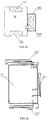
- FIG. la to FIG. 1C are schematic structural diagrams of a wireless terminal according to embodiments of the present invention.
- the wireless terminal includes a PCB 10, a first antenna 101, a second antenna 102, a resonator 103, and a bracket 104.
- the first antenna 101 is located at one side of the PCB 10, the second antenna 102 is located at another side of the PCB 10. Specifically, the first antenna 101 and the second antenna 102 may be separately located at two opposite sides of the PCB 10, as shown in FIG. 1a . In another embodiment, the first antenna 101 and the second antenna 102 may further be located at two adjacent sides of the PCB 10, as shown in FIG. 1b (other components are not shown in the figure).
- the PCB 10 functions as a metal ground of the first antenna 101 and the second antenna 102, where a metal layer may be disposed on an upper surface of the PCB 10, or a metal layer may be disposed on a lower surface of the PCB 10, or a metal layer may further be disposed in the PCB 10.
- a material of the metal layer may be copper, or the like.
- the first antenna 101 and the second antenna 102 may be located on the bracket 104 and be supported by the bracket 104, as shown in FIG. 1a .
- the first antenna 101 and the second antenna 102 may further be located on another independent antenna bracket, where the antenna bracket and the bracket 104 are separate and independent of each other.
- the first antenna 101 and the second antenna 102 may also be hot melted on the PCB 10, as shown in FIG. 1c .
- the resonator 103 is located on the bracket 104 of the wireless terminal, and supported by the bracket 104.
- a ground point of the resonator 103 is located on the PCB 10. Specifically, the ground point may be located at a location between the first antenna 101 and the second antenna 102 and close to an edge of the PCB 10, so as to achieve a better isolation effect.
- a clearance of a certain dimension exists between the resonator 103 and the PCB 10.
- the bracket 104 is configured to support the resonator 103, or may further support the first antenna 101 and the second antenna 102.
- the bracket 104 may have multiple implementation manners. For example:
- the bracket 104 may be disposed on a surface of the PCB 10, where the surface refers to a surface with the largest area on the PCB 10, or a board surface for soldering of a circuit component and the like.
- a surface of the bracket 104 and the surface of the PCB 10 are located on or nearly located on a same horizontal plane.
- the bracket 104 may be a hollow rectangular framework. After the bracket 104 is pressed or buckled on the PCB 10, the PCB 10 is precisely embedded in the hollow position of the rectangular framework.
- the two opposite sides of the bracket 104 may be respectively used to support the first antenna 101 and the second antenna 102, and another side edge of the bracket 104 may be used to support the resonator 103.
- the bracket 104 may be disposed on a side surface perpendicular to the foregoing surface (or the board surface) of the PCB 10, in other words, the bracket 104 is located at one side edge of the PCB 10.
- the bracket 104 is configured to support the resonator 103.
- the bracket 104 may also be separated from the PCB 10, rather than be fastened or connected to the PCB 10.
- the bracket 104 may be fastened or connected to a housing (not shown in the figure) of the wireless terminal, where the housing is a component into which multiple parts of the wireless terminal, such as the PCB 10, the first antenna 101, the second antenna 102, and the resonator 103 are encapsulated.
- the housing may be formed by two components that can be buckled together to form enclosed space.
- the bracket 104 may be fastened or connected in the housing, and configured to support the first antenna 101, the second antenna 102, and the resonator 103.
- the first antenna 101 and second antenna 102 may also be hot melted on the PCB 10.
- the bracket 104 is configured to support the resonator 103.
- the housing of the wireless terminal may also directly serve as the bracket 104.
- the first antenna 101, the second antenna 102, and the resonator 103 may all be directly printed in the housing.
- the first antenna 101 and the second antenna 102 may also be hot melted on the PCB 10, and the resonator 103 is printed in the housing.
- the foregoing brackets 104 may all be plastic brackets.
- a resonator is disposed on a wireless terminal, not only is current distribution of a first antenna and a second antenna on a PCB changed, so that isolation between multiple antennas is improved, but also the resonator can better radiate energy of the antennas because a clearance exists between the resonator and the PCB. Therefore, it is avoided that the energy of the antennas flowing into the resonator is wasted in the resonator, thereby implementing secondary radiation of the energy of the antennas, and improving radiation efficiency of the antennas.
- the resonator may be one or more of, specifically one of or any combination of, the following: a high and low frequency metal open stub, a closed metal stub, a metal stub in a form of a monopole antenna (monopole), or a metal stub in a shape of an inverted-F antenna (Inverted-F Antanna, IFA).
- the resonator is a high and low frequency metal open stub 211, where the high and low frequency metal open stub 211 is of a structure formed by two metal strips extending from an edge of a PCB 21, and the two metal strips form a simple open structure, are compact in size, and are spaced from the PCB 21 by a clearance of a certain size. Of the two metal strips, one is long and the other is short, where the long metal strip, being a branch, resonates at a low frequency, and the short metal strip, being a branch, resonates at a high frequency. In addition, a resonance structure is relatively open, and therefore the resonator can work in multiple frequency bands and a bandwidths is relatively wide.
- the high and low frequency metal open stub 211 is located between a first antenna 212 and a second antenna 213.
- the resonator is another high and low frequency metal open stub 221, where the high and low frequency metal open stub 221 is of a structure in which one metal strip extends from an edge of a PCB 22, and after the extending, the metal strip is split into two metal strips.
- the two metal strips are disposed in parallel, are simple in structure, form an open structure, are compact in size, and are spaced from the PCB 22 by a clearance of a certain size.
- the two metal strips one is long and the other is short, where the long metal strip, being a branch, resonates at a low frequency, and the short metal strip, being a branch, resonates at a high frequency.
- a resonance structure is relatively open, and therefore the resonator can work in multiple frequency bands and a bandwidth is relatively wide.
- the high and low frequency metal open stub 221 is located between a first antenna 222 and a second antenna 223.
- the resonator is a closed metal stub 311, that is, a metal stub in a Loop form.
- the closed metal stub 311 is of a structure formed by a metal strip that extends from an edge of a PCB 30 and is in a shape of a closed Loop, and the metal strip in the shape of the Loop forms an open structure.
- a resonance frequency of a working fundamental mode (1 wavelength) of the closed metal stub 311 is at a low frequency, which may work at the low frequency
- a resonance point of a higher order mode (3/2 wavelengths) of the resonator is at a high frequency
- the higher order mode of the resonator may work at the high frequency.
- the metal strip is of a simple structure, and is spaced from the PCB 30 by a clearance of a certain size, featuring sound radiation efficiency.
- the closed metal stub 311 is located between a first antenna 312 and a second antenna 313.
- the resonator is a metal stub 411 in a monopole form, where the metal stub 411 is of a structure of a C-shaped metal strip extending from an edge of a PCB 40, and the C-shaped metal strip form an open structure.
- a resonance point of the metal stub 411 may be close to a low frequency of 800 Mhz, a resonance point of a higher order mode (2 wavelengths) is at a high frequency, and therefore, the metal stub 411 can work at the low frequency, and the higher order mode of the resonator can work at the high frequency.
- the metal strip is of a simple structure, and is spaced from the PCB 40 by a clearance of a certain size, featuring sound radiation efficiency.
- the metal stub 411 in the monopole form is located between a first antenna 412 and a second antenna 413.
- the resonator may further be electrically connected to a lump component, and the lump component may specifically be a capacitor or an inductor, or the like.
- One end of the lump component may be electrically connected to a junction between the resonator and the PCB, and specifically may be electrically connected to an endpoint of a metal strip of the resonator, and another end is grounded.
- the lump component may enable a working frequency of the resonator to be closer to a low frequency, thereby effectively reducing a structural size of the resonator.
- the resonator 51 may be electrically connected to a lump component 53 through a switch assembly 52, and the lump component 53 may be located on the PCB, where the lump component 53 includes at least two matching circuits, different matching circuits correspond to different working frequencies, and the switch assembly 52 may switch between multiple matching circuits, so that a resonance point of the resonator 51 that is of an open structure may switch between the working frequencies that correspond to the matching circuits.
- the resonator 61 that is of an open structure is electrically connected to a lump component 63 through a switch assembly 62.
- the lump component 63 includes two matching circuits 631 and 632, where an SMT inductor is connected in series in the matching circuit 631, a chip capacitor is connected in series in the matching circuit 632, the two matching circuits correspond to different working frequencies, and the switch assembly 62 may switch between the matching circuits 631 and 632, so that a resonance point of the resonator 61 that is of an open structure may switch between working frequencies corresponding to the matching circuits 631 and 632.
- a switch assembly switches between different matching circuits, so that a resonance point of a resonator can switch between different frequencies, therefore isolation between antennas under different frequencies can be improved, and a bandwidth is increased effectively without increasing space of the resonator.
- brackets are not shown.
- the brackets in the foregoing embodiments may all be implemented by using any one of the manners of the brackets in the embodiments described above.
- the wireless terminal according to the embodiments of the present invention may be a mobile terminal such as a mobile phone, CPE, or a gateway.
- the wireless terminal may improve isolation between multiple antennas and multiple frequency bands, and also improve the radiation efficiency of an antenna, and may improve SAR and HAC performance.
- the disclosed system, apparatus, and method may be implemented in other manners.
- the described apparatus embodiment is merely exemplary.
- the unit division is merely logical function division and may be other division in actual implementation.
- a plurality of units or components may be combined or integrated into another system, or some features may be ignored or not performed.
- the displayed or discussed mutual couplings or direct couplings or communication connections may be implemented through some interfaces.
- the indirect couplings or communication connections between the apparatuses or units may be implemented in electronic, mechanical, or other forms.
- the units described as separate parts may or may not be physically separate, and parts displayed as units may or may not be physical units, may be located in one position, or may be distributed on a plurality of network units. A part or all of the units may be selected according to actual needs to achieve the objectives of the solutions of the embodiments.
- functional units in the embodiments of the present invention may be integrated into one processing unit, or each of the units may exist alone physically, or two or more units are integrated into one unit.
Landscapes
- Engineering & Computer Science (AREA)
- Computer Networks & Wireless Communication (AREA)
- Physics & Mathematics (AREA)
- Electromagnetism (AREA)
- Support Of Aerials (AREA)
- Details Of Aerials (AREA)
- Variable-Direction Aerials And Aerial Arrays (AREA)
- Transceivers (AREA)
Claims (10)
- Terminal sans fil, comprenant une première antenne (101), une seconde antenne (102), une carte de circuit imprimé (10), un support (104) et un résonateur (103), dans lequel la première antenne est située sur un côté de la carte de circuit imprimé, la seconde antenne est située sur un autre côté de la carte de circuit imprimé, la carte de circuit imprimé fait office de masse métallique de la première antenne et de la seconde antenne, caractérisé en ce que le résonateur est situé sur le support, un point de masse du résonateur est situé sur la carte de circuit imprimé et un espace existe entre le résonateur et la carte de circuit imprimé, le support étant un support en plastique.
- Terminal sans fil selon la revendication 1, dans lequel le support est disposé sur une surface de la carte de circuit imprimé ou est disposé sur une surface latérale de la carte de circuit imprimé qui est perpendiculaire à la surface.
- Terminal sans fil selon la revendication 1, dans lequel le terminal sans fil comprend en outre un boîtier et le support est disposé sur le boîtier du terminal sans fil.
- Terminal sans fil selon la revendication 1, dans lequel le support est le boîtier du terminal sans fil.
- Terminal sans fil selon l'une quelconque des revendications 1 à 4, dans lequel une couche métallique est disposée sur une surface supérieure de la carte de circuit imprimé ou une couche métallique est disposée sur une surface inférieure de la carte de circuit imprimé ou une couche métallique est disposée dans la carte de circuit imprimé.
- Terminal sans fil selon l'une quelconque des revendications 1 à 5, dans lequel, lorsque la première antenne est située sur un côté de la carte de circuit imprimé et que la seconde antenne est disposée sur un autre côté de la carte de circuit imprimé, c'est de façon précise :la première antenne et la seconde antenne qui sont situées de façon séparée sur les deux côtés opposés de la carte de circuit imprimé; oula première antenne et la seconde antenne qui sont situées de façon séparée sur les deux côtés adjacents de la carte de circuit imprimé.
- Terminal sans fil selon l'une quelconque des revendications 1 à 6, dans lequel lorsqu'un point de masse du résonateur est situé sur la carte de circuit imprimé, c'est de façon précise :le point de masse du résonateur qui est situé sur la carte de circuit imprimé (10) et entre la première antenne et la seconde antenne.
- Terminal sans fil selon l'une quelconque des revendications 1 à 7, dans lequel le résonateur est, de façon précise, un élément ou une combinaison quelconque des éléments suivants :une embase métallique ouverte de haute et basse fréquence (211), (221), une embase métallique fermée (311), une embase métallique sous la forme d'une antenne unipolaire (411) ou une embase métallique sous la forme d'une antenne en F inversé.
- Terminal sans fil selon l'une quelconque des revendications 1 à 8, dans lequel le résonateur est raccordé électriquement à un composant formant bosse (53) et le composant formant bosse est situé sur la carte de circuit imprimé.
- Terminal sans fil selon la revendication 9, dans lequel le résonateur est raccordé électriquement au composant formant bosse au moyen d'un ensemble commutateur, dans lequel le composant formant bosse comprend au moins deux circuits d'adaptation, différents circuits d'adaptation correspondent à différentes fréquences de fonctionnement, et l'ensemble commutateur (52) est configuré pour commuter entre les deux, ou plus, circuits d'adaptation de sorte à permettre à un point de résonance du résonateur de commuter entre les fréquences de fonctionnement correspondant aux circuits d'adaptation.
Priority Applications (3)
| Application Number | Priority Date | Filing Date | Title |
|---|---|---|---|
| ES17159650T ES2715201T3 (es) | 2013-07-30 | 2013-07-30 | Terminal inalámbrico |
| EP18198014.5A EP3499730B1 (fr) | 2013-07-30 | 2013-07-30 | Terminal sans fil |
| EP17159650.5A EP3242408B1 (fr) | 2013-07-30 | 2013-07-30 | Terminal sans fil |
Applications Claiming Priority (3)
| Application Number | Priority Date | Filing Date | Title |
|---|---|---|---|
| EP17159650.5A EP3242408B1 (fr) | 2013-07-30 | 2013-07-30 | Terminal sans fil |
| EP13882056.8A EP2950455B1 (fr) | 2013-07-30 | 2013-07-30 | Terminal sans fil |
| PCT/CN2013/080395 WO2015013880A1 (fr) | 2013-07-30 | 2013-07-30 | Terminal sans fil |
Related Parent Applications (2)
| Application Number | Title | Priority Date | Filing Date |
|---|---|---|---|
| EP13882056.8A Division-Into EP2950455B1 (fr) | 2013-07-30 | 2013-07-30 | Terminal sans fil |
| EP13882056.8A Division EP2950455B1 (fr) | 2013-07-30 | 2013-07-30 | Terminal sans fil |
Related Child Applications (2)
| Application Number | Title | Priority Date | Filing Date |
|---|---|---|---|
| EP18198014.5A Division EP3499730B1 (fr) | 2013-07-30 | 2013-07-30 | Terminal sans fil |
| EP18198014.5A Division-Into EP3499730B1 (fr) | 2013-07-30 | 2013-07-30 | Terminal sans fil |
Publications (2)
| Publication Number | Publication Date |
|---|---|
| EP3242408A1 EP3242408A1 (fr) | 2017-11-08 |
| EP3242408B1 true EP3242408B1 (fr) | 2018-12-19 |
Family
ID=50215549
Family Applications (3)
| Application Number | Title | Priority Date | Filing Date |
|---|---|---|---|
| EP13882056.8A Active EP2950455B1 (fr) | 2013-07-30 | 2013-07-30 | Terminal sans fil |
| EP17159650.5A Active EP3242408B1 (fr) | 2013-07-30 | 2013-07-30 | Terminal sans fil |
| EP18198014.5A Active EP3499730B1 (fr) | 2013-07-30 | 2013-07-30 | Terminal sans fil |
Family Applications Before (1)
| Application Number | Title | Priority Date | Filing Date |
|---|---|---|---|
| EP13882056.8A Active EP2950455B1 (fr) | 2013-07-30 | 2013-07-30 | Terminal sans fil |
Family Applications After (1)
| Application Number | Title | Priority Date | Filing Date |
|---|---|---|---|
| EP18198014.5A Active EP3499730B1 (fr) | 2013-07-30 | 2013-07-30 | Terminal sans fil |
Country Status (6)
| Country | Link |
|---|---|
| US (3) | US9698470B2 (fr) |
| EP (3) | EP2950455B1 (fr) |
| JP (1) | JP6122503B2 (fr) |
| CN (1) | CN103636064B (fr) |
| ES (1) | ES2715201T3 (fr) |
| WO (1) | WO2015013880A1 (fr) |
Families Citing this family (21)
| Publication number | Priority date | Publication date | Assignee | Title |
|---|---|---|---|---|
| JP6122503B2 (ja) * | 2013-07-30 | 2017-04-26 | ▲華▼▲為▼終端有限公司Huawei Device Co., Ltd. | 無線端末 |
| TWI539663B (zh) * | 2014-03-19 | 2016-06-21 | 宏碁股份有限公司 | 手持式裝置 |
| CN104953234B (zh) * | 2014-03-26 | 2018-02-09 | 宏碁股份有限公司 | 手持式装置 |
| US9991585B2 (en) | 2014-04-28 | 2018-06-05 | Huawei Device (Dongguan) Co., Ltd. | Antenna apparatus and terminal |
| WO2015172296A1 (fr) * | 2014-05-12 | 2015-11-19 | 华为技术有限公司 | Appareil d'antenne et dispositif électronique |
| CN105226371B (zh) * | 2014-05-26 | 2019-02-26 | 比亚迪股份有限公司 | 用于电子设备的天线系统和具有该天线系统的电子设备 |
| US9548525B2 (en) * | 2015-01-13 | 2017-01-17 | Futurewei Technologies, Inc. | Multi-band antenna on the surface of wireless communication devices |
| TWI584627B (zh) * | 2015-02-04 | 2017-05-21 | 耀登科技股份有限公司 | 通訊裝置 |
| WO2017008247A1 (fr) * | 2015-07-14 | 2017-01-19 | 华为技术有限公司 | Terminal mobile |
| CN205122751U (zh) * | 2015-09-23 | 2016-03-30 | 西安中兴新软件有限责任公司 | 一种天线装置和移动终端 |
| CN206148075U (zh) | 2016-10-28 | 2017-05-03 | 京东方科技集团股份有限公司 | 一种显示装置 |
| TWI658649B (zh) * | 2017-12-06 | 2019-05-01 | Acer Incorporated | 無線電子裝置 |
| TWM566918U (zh) * | 2018-04-20 | 2018-09-11 | 明泰科技股份有限公司 | Antenna architecture with low trace path |
| CN110931973A (zh) * | 2018-09-20 | 2020-03-27 | 中兴通讯股份有限公司 | 终端 |
| CN111342242B (zh) * | 2018-12-19 | 2021-09-03 | 华硕电脑股份有限公司 | 多天线系统及其电子装置 |
| CN110970706B (zh) * | 2019-11-20 | 2021-04-09 | 珠海格力电器股份有限公司 | 多模天线、终端、多模天线的通信方法及装置及处理器 |
| CN111029771B (zh) * | 2019-12-31 | 2021-08-17 | 上海创功通讯技术有限公司 | 一种手表天线及手表 |
| EP4358304A4 (fr) * | 2021-09-06 | 2024-10-23 | Samsung Electronics Co., Ltd. | Dispositif de transmission d'énergie sans fil, et procédé de détection d'objet proche d'un dispositif de transmission d'énergie sans fil |
| CN113871839A (zh) * | 2021-09-27 | 2021-12-31 | 东莞华贝电子科技有限公司 | 一种终端设备 |
| JP7568187B2 (ja) * | 2022-02-18 | 2024-10-16 | 広州視源電子科技股▲分▼有限公司 | アンテナアセンブリ及びインタラクティブディスプレイ |
| WO2024172506A1 (fr) * | 2023-02-16 | 2024-08-22 | 삼성전자 주식회사 | Dispositif électronique pouvant être porté sur soi |
Family Cites Families (21)
| Publication number | Priority date | Publication date | Assignee | Title |
|---|---|---|---|---|
| US6956530B2 (en) * | 2002-09-20 | 2005-10-18 | Centurion Wireless Technologies, Inc. | Compact, low profile, single feed, multi-band, printed antenna |
| EP1469554A1 (fr) * | 2003-04-15 | 2004-10-20 | Hewlett-Packard Development Company, L.P. | Dispositif d'antenne monopôle à double entrée |
| EP1625636A1 (fr) * | 2003-05-09 | 2006-02-15 | Philips Intellectual Property & Standards GmbH | Antenne integree a un logement |
| CN1922762A (zh) * | 2004-02-25 | 2007-02-28 | 皇家飞利浦电子股份有限公司 | 天线模块 |
| US7330156B2 (en) * | 2004-08-20 | 2008-02-12 | Nokia Corporation | Antenna isolation using grounded microwave elements |
| JP4146478B2 (ja) * | 2006-07-07 | 2008-09-10 | 株式会社東芝 | 無線モジュール及び携帯端末 |
| US8525734B2 (en) * | 2006-12-21 | 2013-09-03 | Nokia Corporation | Antenna device |
| CN101005291B (zh) * | 2007-01-19 | 2010-05-19 | 清华大学 | 移动终端双频平面两天线系统 |
| JP4966125B2 (ja) * | 2007-07-27 | 2012-07-04 | 株式会社東芝 | アンテナ装置及び無線機 |
| JP5104131B2 (ja) * | 2007-08-31 | 2012-12-19 | 富士通セミコンダクター株式会社 | 無線装置および無線装置が備えるアンテナ |
| EP2565982B1 (fr) | 2008-02-14 | 2019-03-20 | Zinwave Limited | Système de communication |
| JP2009246560A (ja) * | 2008-03-28 | 2009-10-22 | Ngk Spark Plug Co Ltd | アンテナ装置及びそれを備えた無線通信装置 |
| JP2011120071A (ja) * | 2009-12-04 | 2011-06-16 | Panasonic Corp | 携帯無線機 |
| CN201868674U (zh) | 2010-08-10 | 2011-06-15 | 富士康(昆山)电脑接插件有限公司 | 线缆连接器组件 |
| CN201868574U (zh) * | 2010-09-08 | 2011-06-15 | 惠州Tcl移动通信有限公司 | 一种多频段天线 |
| EP2518824A1 (fr) * | 2011-04-27 | 2012-10-31 | Research In Motion Limited | Ensemble formant antenne multiple utilisant des structures d'isolation à bande interdite électromagnétique |
| US8714459B2 (en) * | 2011-05-12 | 2014-05-06 | Waveconnex, Inc. | Scalable high-bandwidth connectivity |
| JP2012253641A (ja) * | 2011-06-06 | 2012-12-20 | Mitsubishi Materials Corp | アンテナ装置 |
| KR101879705B1 (ko) * | 2012-01-18 | 2018-07-18 | 삼성전자주식회사 | 휴대용 단말기의 안테나 장치 |
| JP6122503B2 (ja) * | 2013-07-30 | 2017-04-26 | ▲華▼▲為▼終端有限公司Huawei Device Co., Ltd. | 無線端末 |
| CN106832852A (zh) | 2016-12-28 | 2017-06-13 | 深圳天珑无线科技有限公司 | 一种应用于移动设备的中板支架及制备方法和移动设备 |
-
2013
- 2013-07-30 JP JP2015540994A patent/JP6122503B2/ja active Active
- 2013-07-30 EP EP13882056.8A patent/EP2950455B1/fr active Active
- 2013-07-30 EP EP17159650.5A patent/EP3242408B1/fr active Active
- 2013-07-30 CN CN201380001702.5A patent/CN103636064B/zh active Active
- 2013-07-30 ES ES17159650T patent/ES2715201T3/es active Active
- 2013-07-30 WO PCT/CN2013/080395 patent/WO2015013880A1/fr not_active Ceased
- 2013-07-30 EP EP18198014.5A patent/EP3499730B1/fr active Active
-
2014
- 2014-10-23 US US14/522,109 patent/US9698470B2/en active Active
-
2017
- 2017-04-06 US US15/481,059 patent/US10297901B2/en active Active
-
2019
- 2019-04-05 US US16/376,597 patent/US10601116B2/en active Active
Non-Patent Citations (1)
| Title |
|---|
| None * |
Also Published As
| Publication number | Publication date |
|---|---|
| US20170214124A1 (en) | 2017-07-27 |
| CN103636064A (zh) | 2014-03-12 |
| US10297901B2 (en) | 2019-05-21 |
| EP3499730A1 (fr) | 2019-06-19 |
| US10601116B2 (en) | 2020-03-24 |
| JP2016504796A (ja) | 2016-02-12 |
| EP2950455A1 (fr) | 2015-12-02 |
| ES2715201T3 (es) | 2019-06-03 |
| EP2950455A4 (fr) | 2016-02-17 |
| EP2950455B1 (fr) | 2017-05-10 |
| WO2015013880A1 (fr) | 2015-02-05 |
| US20190229407A1 (en) | 2019-07-25 |
| US20150042520A1 (en) | 2015-02-12 |
| US9698470B2 (en) | 2017-07-04 |
| EP3242408A1 (fr) | 2017-11-08 |
| CN103636064B (zh) | 2015-11-25 |
| JP6122503B2 (ja) | 2017-04-26 |
| EP3499730B1 (fr) | 2020-07-22 |
Similar Documents
| Publication | Publication Date | Title |
|---|---|---|
| US10601116B2 (en) | Wireless terminal | |
| US10601117B2 (en) | Antenna and mobile terminal | |
| EP3790110B1 (fr) | Antenne et terminal mobile | |
| CN104795623B (zh) | 移动装置及其制造方法 | |
| CN103117452B (zh) | 一种新型lte终端天线 | |
| CN110492237B (zh) | 基于金属边框的mimo天线结构及移动设备 | |
| TWI599095B (zh) | 天線結構及應用該天線結構的無線通訊裝置 | |
| EP4152517B1 (fr) | Antenne de terminal et dispositif électronique de terminal | |
| CN103151601B (zh) | 一种底边槽耦合天线 | |
| US10236558B2 (en) | LTE full-band cellphone antenna structure | |
| EP3300170B1 (fr) | Antenne et équipement d'utilisateur | |
| EP2713440B1 (fr) | Terminal portable et antenne fendue associée | |
| CN104051841A (zh) | 增强型高效3g/4g/lte天线,设备以及相关的方法 | |
| CN106159422A (zh) | 印刷式耦合馈入多频天线以及电子系统 | |
| CN204257819U (zh) | 多频段宽频抗金属天线 | |
| CN203521611U (zh) | 一种耦合馈电多频天线 | |
| CN113078445B (zh) | 天线结构及具有该天线结构的无线通信装置 | |
| CN102624947A (zh) | 手机天线及其手机 | |
| TWI784678B (zh) | 支援寬頻操作之行動裝置 | |
| Yoon et al. | Compact broadband coupled line antenna for GSM850/900 | |
| TWM363089U (en) | Dual-band antenna |
Legal Events
| Date | Code | Title | Description |
|---|---|---|---|
| PUAI | Public reference made under article 153(3) epc to a published international application that has entered the european phase |
Free format text: ORIGINAL CODE: 0009012 |
|
| STAA | Information on the status of an ep patent application or granted ep patent |
Free format text: STATUS: THE APPLICATION HAS BEEN PUBLISHED |
|
| AC | Divisional application: reference to earlier application |
Ref document number: 2950455 Country of ref document: EP Kind code of ref document: P |
|
| AK | Designated contracting states |
Kind code of ref document: A1 Designated state(s): AL AT BE BG CH CY CZ DE DK EE ES FI FR GB GR HR HU IE IS IT LI LT LU LV MC MK MT NL NO PL PT RO RS SE SI SK SM TR |
|
| RAP1 | Party data changed (applicant data changed or rights of an application transferred) |
Owner name: HUAWEI DEVICE (DONGGUAN) CO., LTD. |
|
| STAA | Information on the status of an ep patent application or granted ep patent |
Free format text: STATUS: REQUEST FOR EXAMINATION WAS MADE |
|
| 17P | Request for examination filed |
Effective date: 20180508 |
|
| RBV | Designated contracting states (corrected) |
Designated state(s): AL AT BE BG CH CY CZ DE DK EE ES FI FR GB GR HR HU IE IS IT LI LT LU LV MC MK MT NL NO PL PT RO RS SE SI SK SM TR |
|
| GRAP | Despatch of communication of intention to grant a patent |
Free format text: ORIGINAL CODE: EPIDOSNIGR1 |
|
| STAA | Information on the status of an ep patent application or granted ep patent |
Free format text: STATUS: GRANT OF PATENT IS INTENDED |
|
| INTG | Intention to grant announced |
Effective date: 20180702 |
|
| GRAS | Grant fee paid |
Free format text: ORIGINAL CODE: EPIDOSNIGR3 |
|
| GRAA | (expected) grant |
Free format text: ORIGINAL CODE: 0009210 |
|
| STAA | Information on the status of an ep patent application or granted ep patent |
Free format text: STATUS: THE PATENT HAS BEEN GRANTED |
|
| AC | Divisional application: reference to earlier application |
Ref document number: 2950455 Country of ref document: EP Kind code of ref document: P |
|
| AK | Designated contracting states |
Kind code of ref document: B1 Designated state(s): AL AT BE BG CH CY CZ DE DK EE ES FI FR GB GR HR HU IE IS IT LI LT LU LV MC MK MT NL NO PL PT RO RS SE SI SK SM TR |
|
| REG | Reference to a national code |
Ref country code: GB Ref legal event code: FG4D |
|
| REG | Reference to a national code |
Ref country code: CH Ref legal event code: EP |
|
| REG | Reference to a national code |
Ref country code: IE Ref legal event code: FG4D |
|
| REG | Reference to a national code |
Ref country code: DE Ref legal event code: R096 Ref document number: 602013048621 Country of ref document: DE |
|
| REG | Reference to a national code |
Ref country code: AT Ref legal event code: REF Ref document number: 1079791 Country of ref document: AT Kind code of ref document: T Effective date: 20190115 |
|
| REG | Reference to a national code |
Ref country code: SE Ref legal event code: TRGR |
|
| REG | Reference to a national code |
Ref country code: NL Ref legal event code: FP |
|
| PG25 | Lapsed in a contracting state [announced via postgrant information from national office to epo] |
Ref country code: LV Free format text: LAPSE BECAUSE OF FAILURE TO SUBMIT A TRANSLATION OF THE DESCRIPTION OR TO PAY THE FEE WITHIN THE PRESCRIBED TIME-LIMIT Effective date: 20181219 Ref country code: NO Free format text: LAPSE BECAUSE OF FAILURE TO SUBMIT A TRANSLATION OF THE DESCRIPTION OR TO PAY THE FEE WITHIN THE PRESCRIBED TIME-LIMIT Effective date: 20190319 Ref country code: LT Free format text: LAPSE BECAUSE OF FAILURE TO SUBMIT A TRANSLATION OF THE DESCRIPTION OR TO PAY THE FEE WITHIN THE PRESCRIBED TIME-LIMIT Effective date: 20181219 Ref country code: HR Free format text: LAPSE BECAUSE OF FAILURE TO SUBMIT A TRANSLATION OF THE DESCRIPTION OR TO PAY THE FEE WITHIN THE PRESCRIBED TIME-LIMIT Effective date: 20181219 Ref country code: FI Free format text: LAPSE BECAUSE OF FAILURE TO SUBMIT A TRANSLATION OF THE DESCRIPTION OR TO PAY THE FEE WITHIN THE PRESCRIBED TIME-LIMIT Effective date: 20181219 |
|
| REG | Reference to a national code |
Ref country code: LT Ref legal event code: MG4D |
|
| REG | Reference to a national code |
Ref country code: CH Ref legal event code: PFA Owner name: HUAWEI DEVICE CO., LTD., CN Free format text: FORMER OWNER: HUAWEI DEVICE (DONGGUAN) CO., LTD., CN |
|
| PG25 | Lapsed in a contracting state [announced via postgrant information from national office to epo] |
Ref country code: RS Free format text: LAPSE BECAUSE OF FAILURE TO SUBMIT A TRANSLATION OF THE DESCRIPTION OR TO PAY THE FEE WITHIN THE PRESCRIBED TIME-LIMIT Effective date: 20181219 Ref country code: GR Free format text: LAPSE BECAUSE OF FAILURE TO SUBMIT A TRANSLATION OF THE DESCRIPTION OR TO PAY THE FEE WITHIN THE PRESCRIBED TIME-LIMIT Effective date: 20190320 Ref country code: AL Free format text: LAPSE BECAUSE OF FAILURE TO SUBMIT A TRANSLATION OF THE DESCRIPTION OR TO PAY THE FEE WITHIN THE PRESCRIBED TIME-LIMIT Effective date: 20181219 |
|
| REG | Reference to a national code |
Ref country code: ES Ref legal event code: FG2A Ref document number: 2715201 Country of ref document: ES Kind code of ref document: T3 Effective date: 20190603 |
|
| RAP2 | Party data changed (patent owner data changed or rights of a patent transferred) |
Owner name: HUAWEI DEVICE CO., LTD. |
|
| REG | Reference to a national code |
Ref country code: NL Ref legal event code: HC Owner name: HUAWEI DEVICE CO., LTD.; CN Free format text: DETAILS ASSIGNMENT: CHANGE OF OWNER(S), CHANGE OF OWNER(S) NAME; FORMER OWNER NAME: HUAWEI DEVICE (DONGGUAN) CO., LTD. Effective date: 20190514 |
|
| REG | Reference to a national code |
Ref country code: DE Ref legal event code: R081 Ref document number: 602013048621 Country of ref document: DE Owner name: HUAWEI DEVICE CO., LTD., DONGGUAN, CN Free format text: FORMER OWNER: HUAWEI DEVICE (DONGGUAN) CO., LTD., DONGGUAN, GUANGDONG, CN |
|
| REG | Reference to a national code |
Ref country code: BE Ref legal event code: HC Owner name: HUAWEI DEVICE CO., LTD.; CN Free format text: DETAILS ASSIGNMENT: CHANGE OF OWNER(S), CHANGEMENT DE NOM DU PROPRIETAIRE; FORMER OWNER NAME: HUAWEI DEVICE (DONGGUAN) CO., LTD. Effective date: 20190531 |
|
| PG25 | Lapsed in a contracting state [announced via postgrant information from national office to epo] |
Ref country code: PT Free format text: LAPSE BECAUSE OF FAILURE TO SUBMIT A TRANSLATION OF THE DESCRIPTION OR TO PAY THE FEE WITHIN THE PRESCRIBED TIME-LIMIT Effective date: 20190419 Ref country code: PL Free format text: LAPSE BECAUSE OF FAILURE TO SUBMIT A TRANSLATION OF THE DESCRIPTION OR TO PAY THE FEE WITHIN THE PRESCRIBED TIME-LIMIT Effective date: 20181219 |
|
| PG25 | Lapsed in a contracting state [announced via postgrant information from national office to epo] |
Ref country code: SK Free format text: LAPSE BECAUSE OF FAILURE TO SUBMIT A TRANSLATION OF THE DESCRIPTION OR TO PAY THE FEE WITHIN THE PRESCRIBED TIME-LIMIT Effective date: 20181219 Ref country code: RO Free format text: LAPSE BECAUSE OF FAILURE TO SUBMIT A TRANSLATION OF THE DESCRIPTION OR TO PAY THE FEE WITHIN THE PRESCRIBED TIME-LIMIT Effective date: 20181219 Ref country code: IS Free format text: LAPSE BECAUSE OF FAILURE TO SUBMIT A TRANSLATION OF THE DESCRIPTION OR TO PAY THE FEE WITHIN THE PRESCRIBED TIME-LIMIT Effective date: 20190419 Ref country code: EE Free format text: LAPSE BECAUSE OF FAILURE TO SUBMIT A TRANSLATION OF THE DESCRIPTION OR TO PAY THE FEE WITHIN THE PRESCRIBED TIME-LIMIT Effective date: 20181219 Ref country code: SM Free format text: LAPSE BECAUSE OF FAILURE TO SUBMIT A TRANSLATION OF THE DESCRIPTION OR TO PAY THE FEE WITHIN THE PRESCRIBED TIME-LIMIT Effective date: 20181219 |
|
| REG | Reference to a national code |
Ref country code: DE Ref legal event code: R097 Ref document number: 602013048621 Country of ref document: DE |
|
| PLBE | No opposition filed within time limit |
Free format text: ORIGINAL CODE: 0009261 |
|
| STAA | Information on the status of an ep patent application or granted ep patent |
Free format text: STATUS: NO OPPOSITION FILED WITHIN TIME LIMIT |
|
| PG25 | Lapsed in a contracting state [announced via postgrant information from national office to epo] |
Ref country code: DK Free format text: LAPSE BECAUSE OF FAILURE TO SUBMIT A TRANSLATION OF THE DESCRIPTION OR TO PAY THE FEE WITHIN THE PRESCRIBED TIME-LIMIT Effective date: 20181219 |
|
| 26N | No opposition filed |
Effective date: 20190920 |
|
| REG | Reference to a national code |
Ref country code: AT Ref legal event code: HC Ref document number: 1079791 Country of ref document: AT Kind code of ref document: T Owner name: HUAWEI DEVICE CO., LTD., CN Effective date: 20191105 |
|
| PG25 | Lapsed in a contracting state [announced via postgrant information from national office to epo] |
Ref country code: SI Free format text: LAPSE BECAUSE OF FAILURE TO SUBMIT A TRANSLATION OF THE DESCRIPTION OR TO PAY THE FEE WITHIN THE PRESCRIBED TIME-LIMIT Effective date: 20181219 Ref country code: MC Free format text: LAPSE BECAUSE OF FAILURE TO SUBMIT A TRANSLATION OF THE DESCRIPTION OR TO PAY THE FEE WITHIN THE PRESCRIBED TIME-LIMIT Effective date: 20181219 |
|
| PG25 | Lapsed in a contracting state [announced via postgrant information from national office to epo] |
Ref country code: TR Free format text: LAPSE BECAUSE OF FAILURE TO SUBMIT A TRANSLATION OF THE DESCRIPTION OR TO PAY THE FEE WITHIN THE PRESCRIBED TIME-LIMIT Effective date: 20181219 |
|
| PG25 | Lapsed in a contracting state [announced via postgrant information from national office to epo] |
Ref country code: LU Free format text: LAPSE BECAUSE OF NON-PAYMENT OF DUE FEES Effective date: 20190730 |
|
| PG25 | Lapsed in a contracting state [announced via postgrant information from national office to epo] |
Ref country code: IE Free format text: LAPSE BECAUSE OF NON-PAYMENT OF DUE FEES Effective date: 20190730 |
|
| PG25 | Lapsed in a contracting state [announced via postgrant information from national office to epo] |
Ref country code: CY Free format text: LAPSE BECAUSE OF FAILURE TO SUBMIT A TRANSLATION OF THE DESCRIPTION OR TO PAY THE FEE WITHIN THE PRESCRIBED TIME-LIMIT Effective date: 20181219 |
|
| PG25 | Lapsed in a contracting state [announced via postgrant information from national office to epo] |
Ref country code: MT Free format text: LAPSE BECAUSE OF FAILURE TO SUBMIT A TRANSLATION OF THE DESCRIPTION OR TO PAY THE FEE WITHIN THE PRESCRIBED TIME-LIMIT Effective date: 20181219 Ref country code: HU Free format text: LAPSE BECAUSE OF FAILURE TO SUBMIT A TRANSLATION OF THE DESCRIPTION OR TO PAY THE FEE WITHIN THE PRESCRIBED TIME-LIMIT; INVALID AB INITIO Effective date: 20130730 |
|
| PG25 | Lapsed in a contracting state [announced via postgrant information from national office to epo] |
Ref country code: MK Free format text: LAPSE BECAUSE OF FAILURE TO SUBMIT A TRANSLATION OF THE DESCRIPTION OR TO PAY THE FEE WITHIN THE PRESCRIBED TIME-LIMIT Effective date: 20181219 |
|
| P01 | Opt-out of the competence of the unified patent court (upc) registered |
Effective date: 20230510 |
|
| REG | Reference to a national code |
Ref country code: AT Ref legal event code: UEP Ref document number: 1079791 Country of ref document: AT Kind code of ref document: T Effective date: 20181219 |
|
| PGFP | Annual fee paid to national office [announced via postgrant information from national office to epo] |
Ref country code: GB Payment date: 20250605 Year of fee payment: 13 |
|
| PGFP | Annual fee paid to national office [announced via postgrant information from national office to epo] |
Ref country code: NL Payment date: 20250613 Year of fee payment: 13 Ref country code: BE Payment date: 20250619 Year of fee payment: 13 |
|
| PGFP | Annual fee paid to national office [announced via postgrant information from national office to epo] |
Ref country code: FR Payment date: 20250610 Year of fee payment: 13 |
|
| PGFP | Annual fee paid to national office [announced via postgrant information from national office to epo] |
Ref country code: BG Payment date: 20250613 Year of fee payment: 13 |
|
| PGFP | Annual fee paid to national office [announced via postgrant information from national office to epo] |
Ref country code: SE Payment date: 20250610 Year of fee payment: 13 |
|
| PGFP | Annual fee paid to national office [announced via postgrant information from national office to epo] |
Ref country code: ES Payment date: 20250807 Year of fee payment: 13 |
|
| PGFP | Annual fee paid to national office [announced via postgrant information from national office to epo] |
Ref country code: DE Payment date: 20250604 Year of fee payment: 13 |
|
| PGFP | Annual fee paid to national office [announced via postgrant information from national office to epo] |
Ref country code: IT Payment date: 20250623 Year of fee payment: 13 |
|
| PGFP | Annual fee paid to national office [announced via postgrant information from national office to epo] |
Ref country code: AT Payment date: 20250625 Year of fee payment: 13 |
|
| PGFP | Annual fee paid to national office [announced via postgrant information from national office to epo] |
Ref country code: CH Payment date: 20250801 Year of fee payment: 13 |
|
| PGFP | Annual fee paid to national office [announced via postgrant information from national office to epo] |
Ref country code: CZ Payment date: 20250718 Year of fee payment: 13 |