EP3244258A2 - Ensemble d'affichage - Google Patents
Ensemble d'affichage Download PDFInfo
- Publication number
- EP3244258A2 EP3244258A2 EP17170238.4A EP17170238A EP3244258A2 EP 3244258 A2 EP3244258 A2 EP 3244258A2 EP 17170238 A EP17170238 A EP 17170238A EP 3244258 A2 EP3244258 A2 EP 3244258A2
- Authority
- EP
- European Patent Office
- Prior art keywords
- film
- display assembly
- display
- backlight
- lcd
- Prior art date
- Legal status (The legal status is an assumption and is not a legal conclusion. Google has not performed a legal analysis and makes no representation as to the accuracy of the status listed.)
- Granted
Links
Images




Classifications
-
- G—PHYSICS
- G02—OPTICS
- G02F—OPTICAL DEVICES OR ARRANGEMENTS FOR THE CONTROL OF LIGHT BY MODIFICATION OF THE OPTICAL PROPERTIES OF THE MEDIA OF THE ELEMENTS INVOLVED THEREIN; NON-LINEAR OPTICS; FREQUENCY-CHANGING OF LIGHT; OPTICAL LOGIC ELEMENTS; OPTICAL ANALOGUE/DIGITAL CONVERTERS
- G02F1/00—Devices or arrangements for the control of the intensity, colour, phase, polarisation or direction of light arriving from an independent light source, e.g. switching, gating or modulating; Non-linear optics
- G02F1/01—Devices or arrangements for the control of the intensity, colour, phase, polarisation or direction of light arriving from an independent light source, e.g. switching, gating or modulating; Non-linear optics for the control of the intensity, phase, polarisation or colour
- G02F1/13—Devices or arrangements for the control of the intensity, colour, phase, polarisation or direction of light arriving from an independent light source, e.g. switching, gating or modulating; Non-linear optics for the control of the intensity, phase, polarisation or colour based on liquid crystals, e.g. single liquid crystal display cells
- G02F1/133—Constructional arrangements; Operation of liquid crystal cells; Circuit arrangements
- G02F1/1333—Constructional arrangements; Manufacturing methods
- G02F1/1335—Structural association of cells with optical devices, e.g. polarisers or reflectors
- G02F1/1336—Illuminating devices
- G02F1/133602—Direct backlight
- G02F1/133606—Direct backlight including a specially adapted diffusing, scattering or light controlling members
-
- G—PHYSICS
- G02—OPTICS
- G02F—OPTICAL DEVICES OR ARRANGEMENTS FOR THE CONTROL OF LIGHT BY MODIFICATION OF THE OPTICAL PROPERTIES OF THE MEDIA OF THE ELEMENTS INVOLVED THEREIN; NON-LINEAR OPTICS; FREQUENCY-CHANGING OF LIGHT; OPTICAL LOGIC ELEMENTS; OPTICAL ANALOGUE/DIGITAL CONVERTERS
- G02F1/00—Devices or arrangements for the control of the intensity, colour, phase, polarisation or direction of light arriving from an independent light source, e.g. switching, gating or modulating; Non-linear optics
- G02F1/01—Devices or arrangements for the control of the intensity, colour, phase, polarisation or direction of light arriving from an independent light source, e.g. switching, gating or modulating; Non-linear optics for the control of the intensity, phase, polarisation or colour
- G02F1/13—Devices or arrangements for the control of the intensity, colour, phase, polarisation or direction of light arriving from an independent light source, e.g. switching, gating or modulating; Non-linear optics for the control of the intensity, phase, polarisation or colour based on liquid crystals, e.g. single liquid crystal display cells
- G02F1/133—Constructional arrangements; Operation of liquid crystal cells; Circuit arrangements
- G02F1/1333—Constructional arrangements; Manufacturing methods
- G02F1/1335—Structural association of cells with optical devices, e.g. polarisers or reflectors
- G02F1/133504—Diffusing, scattering, diffracting elements
-
- G—PHYSICS
- G02—OPTICS
- G02F—OPTICAL DEVICES OR ARRANGEMENTS FOR THE CONTROL OF LIGHT BY MODIFICATION OF THE OPTICAL PROPERTIES OF THE MEDIA OF THE ELEMENTS INVOLVED THEREIN; NON-LINEAR OPTICS; FREQUENCY-CHANGING OF LIGHT; OPTICAL LOGIC ELEMENTS; OPTICAL ANALOGUE/DIGITAL CONVERTERS
- G02F1/00—Devices or arrangements for the control of the intensity, colour, phase, polarisation or direction of light arriving from an independent light source, e.g. switching, gating or modulating; Non-linear optics
- G02F1/01—Devices or arrangements for the control of the intensity, colour, phase, polarisation or direction of light arriving from an independent light source, e.g. switching, gating or modulating; Non-linear optics for the control of the intensity, phase, polarisation or colour
- G02F1/13—Devices or arrangements for the control of the intensity, colour, phase, polarisation or direction of light arriving from an independent light source, e.g. switching, gating or modulating; Non-linear optics for the control of the intensity, phase, polarisation or colour based on liquid crystals, e.g. single liquid crystal display cells
- G02F1/133—Constructional arrangements; Operation of liquid crystal cells; Circuit arrangements
- G02F1/1333—Constructional arrangements; Manufacturing methods
- G02F1/1335—Structural association of cells with optical devices, e.g. polarisers or reflectors
- G02F1/133509—Filters, e.g. light shielding masks
- G02F1/133512—Light shielding layers, e.g. black matrix
-
- G—PHYSICS
- G02—OPTICS
- G02F—OPTICAL DEVICES OR ARRANGEMENTS FOR THE CONTROL OF LIGHT BY MODIFICATION OF THE OPTICAL PROPERTIES OF THE MEDIA OF THE ELEMENTS INVOLVED THEREIN; NON-LINEAR OPTICS; FREQUENCY-CHANGING OF LIGHT; OPTICAL LOGIC ELEMENTS; OPTICAL ANALOGUE/DIGITAL CONVERTERS
- G02F1/00—Devices or arrangements for the control of the intensity, colour, phase, polarisation or direction of light arriving from an independent light source, e.g. switching, gating or modulating; Non-linear optics
- G02F1/01—Devices or arrangements for the control of the intensity, colour, phase, polarisation or direction of light arriving from an independent light source, e.g. switching, gating or modulating; Non-linear optics for the control of the intensity, phase, polarisation or colour
- G02F1/13—Devices or arrangements for the control of the intensity, colour, phase, polarisation or direction of light arriving from an independent light source, e.g. switching, gating or modulating; Non-linear optics for the control of the intensity, phase, polarisation or colour based on liquid crystals, e.g. single liquid crystal display cells
- G02F1/133—Constructional arrangements; Operation of liquid crystal cells; Circuit arrangements
- G02F1/1333—Constructional arrangements; Manufacturing methods
- G02F1/133308—Support structures for LCD panels, e.g. frames or bezels
- G02F1/133331—Cover glasses
-
- G—PHYSICS
- G02—OPTICS
- G02F—OPTICAL DEVICES OR ARRANGEMENTS FOR THE CONTROL OF LIGHT BY MODIFICATION OF THE OPTICAL PROPERTIES OF THE MEDIA OF THE ELEMENTS INVOLVED THEREIN; NON-LINEAR OPTICS; FREQUENCY-CHANGING OF LIGHT; OPTICAL LOGIC ELEMENTS; OPTICAL ANALOGUE/DIGITAL CONVERTERS
- G02F1/00—Devices or arrangements for the control of the intensity, colour, phase, polarisation or direction of light arriving from an independent light source, e.g. switching, gating or modulating; Non-linear optics
- G02F1/01—Devices or arrangements for the control of the intensity, colour, phase, polarisation or direction of light arriving from an independent light source, e.g. switching, gating or modulating; Non-linear optics for the control of the intensity, phase, polarisation or colour
- G02F1/13—Devices or arrangements for the control of the intensity, colour, phase, polarisation or direction of light arriving from an independent light source, e.g. switching, gating or modulating; Non-linear optics for the control of the intensity, phase, polarisation or colour based on liquid crystals, e.g. single liquid crystal display cells
- G02F1/133—Constructional arrangements; Operation of liquid crystal cells; Circuit arrangements
- G02F1/1333—Constructional arrangements; Manufacturing methods
- G02F1/1335—Structural association of cells with optical devices, e.g. polarisers or reflectors
- G02F1/13356—Structural association of cells with optical devices, e.g. polarisers or reflectors characterised by the placement of the optical elements
- G02F1/133562—Structural association of cells with optical devices, e.g. polarisers or reflectors characterised by the placement of the optical elements on the viewer side
-
- G—PHYSICS
- G02—OPTICS
- G02F—OPTICAL DEVICES OR ARRANGEMENTS FOR THE CONTROL OF LIGHT BY MODIFICATION OF THE OPTICAL PROPERTIES OF THE MEDIA OF THE ELEMENTS INVOLVED THEREIN; NON-LINEAR OPTICS; FREQUENCY-CHANGING OF LIGHT; OPTICAL LOGIC ELEMENTS; OPTICAL ANALOGUE/DIGITAL CONVERTERS
- G02F1/00—Devices or arrangements for the control of the intensity, colour, phase, polarisation or direction of light arriving from an independent light source, e.g. switching, gating or modulating; Non-linear optics
- G02F1/01—Devices or arrangements for the control of the intensity, colour, phase, polarisation or direction of light arriving from an independent light source, e.g. switching, gating or modulating; Non-linear optics for the control of the intensity, phase, polarisation or colour
- G02F1/13—Devices or arrangements for the control of the intensity, colour, phase, polarisation or direction of light arriving from an independent light source, e.g. switching, gating or modulating; Non-linear optics for the control of the intensity, phase, polarisation or colour based on liquid crystals, e.g. single liquid crystal display cells
- G02F1/133—Constructional arrangements; Operation of liquid crystal cells; Circuit arrangements
- G02F1/1333—Constructional arrangements; Manufacturing methods
- G02F1/1335—Structural association of cells with optical devices, e.g. polarisers or reflectors
- G02F1/1336—Illuminating devices
Definitions
- LCDs liquid crystal displays
- a non-black dead front display assembly includes a display frame, a backlight system supported by the frame, the backlight system configured to generate a backlight illumination, a light mask disposed on the backlight system, the light mask configured to transmit or to block the backlight illumination in response to a control signal, and a film positioned over the light mask, the film configured to reflect an ambient light and to scatter the backlight illumination transmitted through the light mask.
- the scattered backlight illumination causes a first portion of the film to glow where illuminated by the backlight, while a second portion of the film not illuminated by the backlight appears non-glowing.
- a device comprises a sensor and a non-black dead front display assembly, which comprises a display frame, a backlight system supported by the frame, the backlight system configured to generate a backlight illumination, a light mask disposed on the backlight system, the light mask configured to transmit or to block the backlight illumination in response to a control signal, and a film positioned over the light mask, the film configured to reflect an ambient light and to scatter the backlight illumination transmitted through the light mask.
- the scattered backlight illumination causing a first portion of the film to glow while a second portion of the film appears non-glowing as mentioned above.
- Dead fronting has been used in consumer products in an attempt to blend a display into a black or dark background.
- the dead front display is designed to prevent text, graphics, numbers, symbols, user interface elements, or the like, from being visible until they are illuminated by a light source. Accordingly, when the light source is off or not illuminating, a uniform black or nearly black background is visible. If the display is in an area where the background is not black or dark, for example, in an indoor environment such as a home or an office, the display may stand out and not blend harmoniously with the background.
- Some conventional display products may include a light-emitting diode (LED) matrix on a printed circuit board (PCB) behind a white plastic housing to achieve a white or non-black dead front display effect.
- LED light-emitting diode
- PCB printed circuit board
- Some conventional display products may include a light-emitting diode (LED) matrix on a printed circuit board (PCB) behind a white plastic housing to achieve a white or non-black dead front display effect.
- LEDs light-emitting diode
- PCB printed circuit board
- a device includes a dead front display that is capable of achieving white, or more generally, non-black dead-fronted effects, such that text or graphics may be displayed as a glowing white region, that is, a region that displays as a brighter white than other regions of the display on top of a white front surface, for example.
- a glowing white region that is, a region that displays as a brighter white than other regions of the display on top of a white front surface, for example.
- the display may present a uniform cosmetic surface, for example, a white or non-black surface, to a user.
- the graphics may be displayed as a glowing grey region, that is, a brighter shade of grey than other regions of the display on a grey front surface, for example.
- FIG. 1 shows an example of an exploded view of elements of a display before the elements are assembled.
- a display 200 includes a protective layer 201, a film layer 210, and a display frame 205.
- the film layer 210 may include a diffusion layer of a white, grey or light color.
- FIG. 2 shows an example of the assembled display of FIG. 1 .
- the display frame 205 may include a backlight system 206 and a light mask 204.
- the light mask 204 which includes liquid crystal pixels, and the backlight system 206, are included as components of an LCD 207.
- the backlight system 206 is recessed within the display frame 205, and the light mask 204 is positioned on top of the backlight system 206.
- the LCD 207 includes the backlight 206 and the light mask 204 which includes one or more liquid crystal pixels 203, which may be switched between transparent and opaque states in response to control signals.
- the presently disclosed subject matter may also be applicable to other types of displays, such as color LCDs, monochrome or color LEDs, or monochrome or color organic light emitting diode, (OLEDs).
- the monochrome LCD may provide a contrast ratio between light pixels and dark pixels that is higher than that is found on a typical color display.
- the backlight system 206 of the LCD 207 produces light rays normal to the backlight surface.
- the LCD 207 may include a liquid crystal array in which individual pixels may either block or transmit the incident backlight rays, that is, to appear either opaque black or transparent, in response to control signals.
- an individual pixel is opaque black or substantially opaque black, no light or a minimal amount of light exits the display 200 from the backlight system 206 through that pixel.
- the pixel is transparent or substantially transparent, the light from the backlight system 206 exits the display 200.
- the light rays that exit the transparent or substantially transparent pixels would be directly visible to the user 250.
- each liquid crystal pixel in effect acts as an active light mask for the backlight system 206.
- the film 210 may be a layer of ink or film that is printed or laminated on the protective cover 201, a layer of white polyvinyl chloride (PVC), or a layer of white polytetrafluoroethylene (PTFE), for example.
- PVC polyvinyl chloride
- PTFE white polytetrafluoroethylene
- the film 210 provides a dead front effect, that is, when a pixel 203 in the LCD 207 is off and appears opaque black or nearly opaque black, the region of the film 210 above that pixel appears to a user as being white or nearly white because the film 210 reflects and diffuses external ambient light from above the protective layer 201.
- the film 210 also may serve to hide internal details, for example, the boundaries where the light mask 204 of the LCD 207 ends and the frame 205 of the LCD 207 starts.
- FIG. 3 An example of an illustration of the behavior of light in accordance with an implementation as seen by the user is shown in FIG. 3 .
- the backlight rays will hit the dead front film 210 and scatter in all directions.
- the light from the backlight system 206 appears to be as a glowing small portion of the film 210.
- the small portion of the film 210 may glow white, while the rest of the film 210 may appear to be a substantially uniform non-glowing white flat surface on which ambient light is reflected but no backlight is scattered.
- the LCD backlight that is transmitted and scattered from the film 210 is additive to the ambient light being reflected off the film 210.
- colored or grey films may also be used as dead front diffusion films that have sufficient contrast ratios between glowing regions and non-glowing regions of the films.
- the small portion of the film 210 through which the backlight is scattered may produce a glowing grey, that is, a brighter shade of grey, compared to the non-glowing regions of the film on which the ambient light is reflected but no backlight is scattered.
- the film layer 210 may be made as thin as possible, for example, a thickness of less than 0.6 mm.
- the film layer 210 may be formed by using white ink printed onto a clear substrate, where the ink layer is facing the LCD 207, to provide a diffusion layer thickness on the order of 30 microns.
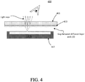
- the distance between the LCD and the diffusion layer may have an impact on the sharpness of the image on the surface of the dead front display system.
- a space is provided between the LCD 407 and the diffusion layer 410, such that backlight rays exiting from the display have more distance to spread out before they hit the diffusion film. For example, if the backlight rays exit the LCD 407 within an angular range of -45 to +45 degrees, then the amount of additional image spread would be proportional to the distance between the LCD 407 and the diffusion film 410.
- FIG. 4 shows an implementation of the display assembly 400 which includes a relatively large gap between the diffusion film 410 and the LCD 407.
- a large gap between the diffusion film and the LCD may result in a blurry image as seen from above the protective layer 401.
- the LCD is close to or in direct contact with the diffusion film, the light is less likely to spread, as illustrated in FIG. 3 , thus producing a clearer image.
- the LCD may be biased by a mechanical structure to cause the LCD to make direct contact with the diffusion film.
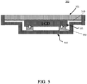
- FIG. 5 shows an example of a display assembly 500 in which the LCD 505 is biased upward to reduce or to eliminate the spacing between the LCD 505 and the diffusion film 510.
- foam or springs 550 on a fixed ledge 560 may be provided beneath the LCD 505 to push the LCD 505 directly against the diffusion film 510, which is supported by a rigid clear front lens 501 as a protective cover.
- This display assembly 500 allows for direct contact between the LCD and the diffusion film even when there is a thickness tolerance on the display and mechanical housing.
- the diffusion film or dead front film 210 may be positioned over the light mask 204.
- the film 210 does not have to be in direct contact with the light mask 204, however.
- the film 210 may be positioned close to the light mask 204 such that the light rays from the backlight system do not spread prior to hitting the film 210. As the separation between the film and the light mask increases, more distance is provided for the light rays from the backlight system to spread out before they hit the film 210. This spread may result in a fuzzier image with a reduced overall brightness as perceived by the user.
- the film may not be bound to the LCD display with an optical adhesive, because the adhesive may be visible to the human eye through the film.
- the film 210 may be applied to the protective cover 201.
- a white ink film may be applied to the surface of the protective cover 201 that is facing the LCD 207.
- the film 210 may be laminated to the protective cover 201, for example.
- a clear protective cover may be used.
- the protective cover 201 may be formed of any material such as plastic, glass, ceramic, or some combination thereof.
- the protective cover 201 may be formed of a transparent material having a sufficient transmissivity which allows the passage of all, most, or at least some light.
- the protective cover may be formed of a material that allows substantially all colors of visible light to pass through it.
- the protective cover 201 may be formed from polymethyl methacrylate (PMMA), also known as acrylic glass.
- PMMA polymethyl methacrylate
- the protective cover 201 and the film 210 may be a part of a single layer.
- the film 210 may be a layer of white PVC on the protective cover 201.
- one or more separate covers may be used to protect the display from external elements.
- a micro-perforated layer of film may be applied to allow sufficient light from the LCD to pass through while preventing external light sources from illuminating the LCD source.
- FIG. 6 shows in an example of an exploded view of elements of a display including a micro-perforated layer prior to assembly.
- FIG. 7 shows a perspective view of the elements of FIG. 6 in an assembled form.
- the display 300 includes a protective cover 301, a white or grey diffusion layer 310, a perforated layer 311 and an LCD 305.
- the perforated layer 311 may be an opaque layer of film or ink with small patterned holes. In some implementations, the perforated layer may also be a diffusion layer.
- the patterned holes may be of any size suitable for transmitting the backlight from the LCD while preventing the ambient light from illuminating the LCD source.
- each hole may be about 0.03 mm in diameter, and the distance between the centers of adjacent holes may be about 0.06 mm.
- the patterned holes may be produced by laser etching or chemical etching, for example, on a layer of a material such as reflective Mylar, metal, plastic, or the like.
- the white or grey layer 310 diffusion may be laminated or printed on one or more solid semi-visible light transparent regions of the perforated layer 311 that represent a cosmetic surface 312, that is, the surface of the perforated layer 311 facing away from the LCD 305.
- FIG. 8 shows an example of transmission and reflection of light rays in the operation of the display arrangement illustrated in FIGs. 6 and 7 .
- ambient light is blocked or reflected off the non-perforated areas of the perforated layer 311 and thus prevented from reaching the LCD source 305.
- the perforated areas of the perforated layer 311 allow the light rays emitted from the backlight of the LCD 305 to be transferred to the cosmetic surface 312 of the perforated layer 311. This allows for sharp images with relatively strong contrasts to be projected through to the surface visible to the user.
- a layer of polarizing material may be disposed between the diffusing film layer and the LCD display.
- the polarizing layer only allows light rays of a given polarity to pass through while reflecting light rays of a polarity that is orthogonal to the given polarity, the visual whiteness or deadness of the device is enhanced when the LCD is in the inactive state, because a greater percentage of the incident light from outside the device is reflected back outward to the diffusing film. That reflected light is then diffused again as it propagates in the outward direction.
- the diffusing film can be made much thinner without sacrificing the visual deadness effect when the LCD is in the inactive state, while at the same time the brightness, crispness, or color performance in the LCD-active state is promoted.
- An implementation of the disclosed display assembly may be included in one or more devices that are part of a smart-home environment, such as a thermostat, alarm control panel, or the like, or part of an automotive environment such as automobile dashboards, or other implementations that may benefit from the user of a dead front display.
- a smart-home environment such as a thermostat, alarm control panel, or the like
- an automotive environment such as automobile dashboards, or other implementations that may benefit from the user of a dead front display.
- Embodiments of the presently disclosed subject matter may be implemented in and used with a variety of devices, for example, a device including the disclosed display assembly.
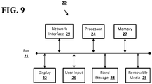
- FIG. 9 shows an example of a device 20 suitable for implementing embodiments of the presently disclosed subject matter.
- the device 20 may be used to implement a controller, a device including sensors such as temperature sensors or alarm sensors in the smart-home environment as disclosed herein, or the like.
- the device 20 may be, for example, a desktop or laptop computer, or a mobile computing device such as a smart phone, tablet, or the like.
- the device 20 may include a bus 21 which interconnects major components of the computer 20, such as a central processor 24, a memory 27 such as Random Access Memory (RAM), Read Only Memory (ROM), flash RAM, or the like, a user display 22 such as a display screen having a non-black dead front display effect, a user input interface 26, which may include one or more controllers and associated user input devices such as a keyboard, mouse, touch screen, and the like, a fixed storage 23 such as a hard drive, flash storage, and the like, a removable media component 25 operative to control and receive an optical disk, flash drive, and the like, and a network interface 29 operable to communicate with one or more remote devices via a suitable network connection.
- a bus 21 which interconnects major components of the computer 20, such as a central processor 24, a memory 27 such as Random Access Memory (RAM), Read Only Memory (ROM), flash RAM, or the like, a user display 22 such as a display screen having a non-black dead front display effect, a user input interface 26, which may include one or more
- the bus 21 allows data communication between the central processor 24 and one or more memory components 25, 27, which may include RAM, ROM, and other memory, as previously noted.
- Applications resident with the computer 20 are generally stored on and accessed via a computer readable storage medium.
- the fixed storage 23 may be integral with the computer 20 or may be separate and accessed through other interfaces.
- the network interface 29 may provide a direct connection to a remote server via a wired or wireless connection.
- the network interface 29 may provide such connection using any suitable technique and protocol as will be readily understood by one of skill in the art, including digital cellular telephone, Wi-Fi, Bluetooth®, near-field, and the like.
- the network interface 29 may allow the device to communicate with other computers via one or more local, wide-area, or other communication networks, as described in further detail herein.
- Various embodiments of the presently disclosed subject matter may include or be embodied in the form of computer-implemented processes and apparatuses for practicing those processes.
- Various embodiments also may be implemented in the form of a computer program product having computer program code containing instructions embodied in non-transitory and/or tangible media, such as hard drives, USB (universal serial bus) drives, or any other machine readable storage medium, such that when the computer program code is loaded into and executed by a computer, the computer becomes an apparatus for practicing embodiments of the disclosed subject matter.
- the computer program code may configure the microprocessor to become a special-purpose device, such as by creation of specific logic circuits as specified by the instructions.
- Embodiments may be implemented using hardware that may include a processor, such as a general purpose microprocessor and/or an Application Specific Integrated Circuit (ASIC) that embodies all or part of the techniques according to embodiments of the disclosed subject matter in hardware and/or firmware.
- the processor may be coupled to memory, such as RAM, ROM, flash memory, a hard disk or any other device capable of storing electronic information.
- the memory may store instructions adapted to be executed by the processor to perform the techniques according to embodiments of the disclosed subject matter.
Landscapes
- Physics & Mathematics (AREA)
- Nonlinear Science (AREA)
- Mathematical Physics (AREA)
- Chemical & Material Sciences (AREA)
- Crystallography & Structural Chemistry (AREA)
- General Physics & Mathematics (AREA)
- Optics & Photonics (AREA)
- Devices For Indicating Variable Information By Combining Individual Elements (AREA)
Applications Claiming Priority (2)
| Application Number | Priority Date | Filing Date | Title |
|---|---|---|---|
| US201662335594P | 2016-05-12 | 2016-05-12 | |
| US15/232,503 US10209563B2 (en) | 2016-05-12 | 2016-08-09 | Non-black dead front display assembly |
Publications (3)
| Publication Number | Publication Date |
|---|---|
| EP3244258A2 true EP3244258A2 (fr) | 2017-11-15 |
| EP3244258A3 EP3244258A3 (fr) | 2018-01-10 |
| EP3244258B1 EP3244258B1 (fr) | 2019-07-10 |
Family
ID=58707305
Family Applications (1)
| Application Number | Title | Priority Date | Filing Date |
|---|---|---|---|
| EP17170238.4A Active EP3244258B1 (fr) | 2016-05-12 | 2017-05-09 | Ensemble d'affichage |
Country Status (2)
| Country | Link |
|---|---|
| US (1) | US10209563B2 (fr) |
| EP (1) | EP3244258B1 (fr) |
Cited By (2)
| Publication number | Priority date | Publication date | Assignee | Title |
|---|---|---|---|---|
| EP3723072A1 (fr) * | 2019-03-21 | 2020-10-14 | Panasonic Intellectual Property Management Co., Ltd. | Dispositif d'affichage |
| US11194429B2 (en) | 2019-09-05 | 2021-12-07 | Panasonic Intellectual Property Management Co., Ltd. | Information display terminal |
Families Citing this family (12)
| Publication number | Priority date | Publication date | Assignee | Title |
|---|---|---|---|---|
| TWI800484B (zh) | 2016-06-28 | 2023-05-01 | 美商康寧公司 | 層壓薄強化玻璃至用於裝飾及顯示器蓋應用的曲面模製塑膠表面 |
| CN115403280B (zh) | 2016-10-25 | 2024-03-19 | 康宁公司 | 用于显示器的冷成形玻璃积层 |
| US11016590B2 (en) | 2017-01-03 | 2021-05-25 | Corning Incorporated | Vehicle interior systems having a curved cover glass and display or touch panel and methods for forming the same |
| KR102445875B1 (ko) | 2017-01-03 | 2022-09-21 | 코닝 인코포레이티드 | 만곡된 커버 유리 및 디스플레이 또는 터치 패널을 갖는 차량 인테리어 시스템 및 이를 형성시키는 방법 |
| CN117962601A (zh) | 2017-07-18 | 2024-05-03 | 康宁公司 | 复杂弯曲玻璃制品的冷成型 |
| EP3681847B1 (fr) | 2017-09-12 | 2025-01-29 | Corning Incorporated | Éléments tactiles pour verre à face isolée et procédés pour les fabriquer |
| US11065960B2 (en) | 2017-09-13 | 2021-07-20 | Corning Incorporated | Curved vehicle displays |
| TWI844520B (zh) | 2017-10-10 | 2024-06-11 | 美商康寧公司 | 具有改善可靠性的彎曲的覆蓋玻璃的車輛內部系統及其形成方法 |
| KR20210032976A (ko) | 2018-07-16 | 2021-03-25 | 코닝 인코포레이티드 | 냉간-벤딩 유리 기판을 갖는 차량 내부 시스템 및 이를 형성하기 위한 방법 |
| EP3828872B1 (fr) | 2019-11-28 | 2023-11-01 | Panasonic Intellectual Property Management Co., Ltd. | Dispositif d'affichage d'informations |
| JP2022178331A (ja) * | 2021-05-20 | 2022-12-02 | 日本精機株式会社 | 表示装置 |
| US20250283990A1 (en) * | 2024-03-08 | 2025-09-11 | Google Llc | Domed thermostat lens assembly |
Family Cites Families (18)
| Publication number | Priority date | Publication date | Assignee | Title |
|---|---|---|---|---|
| KR0163895B1 (ko) | 1995-01-06 | 1999-01-15 | 김광호 | 시야각을 개선한 액정표시장치 |
| US5695269A (en) * | 1996-01-29 | 1997-12-09 | Delco Electronics Corporation | Multi-color display lighting by led |
| JP2000338907A (ja) | 1999-05-28 | 2000-12-08 | Nippon Seiki Co Ltd | 表示板およびその製造方法 |
| US6825828B2 (en) | 2001-02-23 | 2004-11-30 | General Digital Corporation | Backlit LCD monitor |
| TW200710499A (en) | 2005-09-02 | 2007-03-16 | Jemitek Electronics Corp | Backlight unit and method for uniforming brightness thereof |
| WO2007039863A1 (fr) | 2005-10-03 | 2007-04-12 | Koninklijke Philips Electronics N.V. | Appareil afficheur d'image |
| WO2008069181A1 (fr) | 2006-12-05 | 2008-06-12 | Sharp Kabushiki Kaisha | Dispositif d'affichage à cristaux liquides |
| EP2238505A2 (fr) | 2007-09-27 | 2010-10-13 | Nokia Corporation | Changement de l'aspect d'un dispositif électronique |
| KR20130097736A (ko) | 2010-08-05 | 2013-09-03 | 쓰리엠 이노베이티브 프로퍼티즈 컴파니 | 무광택 표면층을 포함하는 다층 필름 및 물품 |
| US8467177B2 (en) | 2010-10-29 | 2013-06-18 | Apple Inc. | Displays with polarizer windows and opaque masking layers for electronic devices |
| TR201807292T4 (tr) * | 2010-12-28 | 2018-06-21 | Koninklijke Philips Nv | Kişisel bakım cihazları için gizli kullanıcı arayüzü ve bunu yapmanın yöntemi. |
| US9063359B2 (en) * | 2012-01-30 | 2015-06-23 | Sony Mobile Communications Ab | Electronic display projection assembly having substantially white off state |
| WO2013146353A1 (fr) | 2012-03-28 | 2013-10-03 | シャープ株式会社 | Film de commande de lumière, dispositif d'affichage et procédé de fabrication de film de commande de lumière |
| US20130314642A1 (en) | 2012-05-23 | 2013-11-28 | Conopco, Inc., D/B/A Unilever | Non-black dead front display |
| US8967834B2 (en) | 2012-05-23 | 2015-03-03 | Iluminage Beauty, Ltd. | Curved dead front display |
| US9808754B2 (en) * | 2014-02-14 | 2017-11-07 | Access Business Group International Llc | Air treatment system |
| US20150360606A1 (en) * | 2014-06-12 | 2015-12-17 | Nthdegree Technologies Worldwide Inc. | Thin flexible led light sheet applications |
| US9366425B2 (en) * | 2014-08-08 | 2016-06-14 | Motorola Solutions, Inc. | Light emitting diode (LED) display for a portable communication device |
-
2016
- 2016-08-09 US US15/232,503 patent/US10209563B2/en active Active
-
2017
- 2017-05-09 EP EP17170238.4A patent/EP3244258B1/fr active Active
Non-Patent Citations (1)
| Title |
|---|
| None |
Cited By (6)
| Publication number | Priority date | Publication date | Assignee | Title |
|---|---|---|---|---|
| EP3723072A1 (fr) * | 2019-03-21 | 2020-10-14 | Panasonic Intellectual Property Management Co., Ltd. | Dispositif d'affichage |
| US11320688B2 (en) | 2019-03-21 | 2022-05-03 | Panasonic Intellectual Property Management Co., Ltd. | Information display device |
| US11340488B2 (en) | 2019-03-21 | 2022-05-24 | Panasonic Intellectual Property Management Co., Ltd. | Information display device |
| US11422402B2 (en) | 2019-03-21 | 2022-08-23 | Panasonic Intellectual Property Management Co., Ltd. | Information display device |
| US11815756B2 (en) | 2019-03-21 | 2023-11-14 | Panasonic Intellectual Property Management Co., Ltd. | Information display device |
| US11194429B2 (en) | 2019-09-05 | 2021-12-07 | Panasonic Intellectual Property Management Co., Ltd. | Information display terminal |
Also Published As
| Publication number | Publication date |
|---|---|
| US20170329182A1 (en) | 2017-11-16 |
| EP3244258B1 (fr) | 2019-07-10 |
| EP3244258A3 (fr) | 2018-01-10 |
| US10209563B2 (en) | 2019-02-19 |
Similar Documents
| Publication | Publication Date | Title |
|---|---|---|
| EP3244258B1 (fr) | Ensemble d'affichage | |
| CN105093580B (zh) | 一种防窥结构、显示面板、背光模组及显示装置 | |
| US10877570B1 (en) | Electronic devices having keys with coherent fiber bundles | |
| US9684163B2 (en) | Methods, systems, and products for illuminating displays | |
| US10012866B2 (en) | Mirror display and electronic device | |
| CN106165002B (zh) | 双模式显示器及制造方法 | |
| US9899001B2 (en) | Display panel, display device having the same, and controlling method thereof | |
| JP2020507105A (ja) | 表示画面、表示装置および携帯端末 | |
| US20140204039A1 (en) | Compositing display | |
| WO2012129504A1 (fr) | Procédé et appareil de dissimulation de capteurs et d'autres composants de dispositifs électroniques | |
| US20170363797A1 (en) | Transparent display with improved contrast and transmission | |
| CA2996034A1 (fr) | Procede et systeme tactile interactif transparent | |
| WO2020194784A1 (fr) | Dispositif d'affichage | |
| CN110189628A (zh) | 一种背光模组及显示装置 | |
| EP3648441B1 (fr) | Dispositif de caméra et terminal mobile | |
| TWI487999B (zh) | 投影螢幕及其投影系統 | |
| US20230161378A1 (en) | Display assembly for terminal device, terminal device and method for operating display assembly | |
| CN108761922A (zh) | 背光模组、液晶显示模组和电子装置 | |
| US10698262B2 (en) | Display apparatus and method for control thereof | |
| KR102201807B1 (ko) | 차량 후방 메시지 표시 장치 및 이의 동작방법 | |
| CN115004090B (zh) | 用于显示装置的制品和显示系统 | |
| JP6597230B2 (ja) | 表示装置 | |
| CN113703524B (zh) | 一种电子设备 | |
| CN209707847U (zh) | 电子设备 | |
| TWM512147U (zh) | 顯示裝置 |
Legal Events
| Date | Code | Title | Description |
|---|---|---|---|
| PUAI | Public reference made under article 153(3) epc to a published international application that has entered the european phase |
Free format text: ORIGINAL CODE: 0009012 |
|
| STAA | Information on the status of an ep patent application or granted ep patent |
Free format text: STATUS: THE APPLICATION HAS BEEN PUBLISHED |
|
| AK | Designated contracting states |
Kind code of ref document: A2 Designated state(s): AL AT BE BG CH CY CZ DE DK EE ES FI FR GB GR HR HU IE IS IT LI LT LU LV MC MK MT NL NO PL PT RO RS SE SI SK SM TR |
|
| AX | Request for extension of the european patent |
Extension state: BA ME |
|
| PUAL | Search report despatched |
Free format text: ORIGINAL CODE: 0009013 |
|
| AK | Designated contracting states |
Kind code of ref document: A3 Designated state(s): AL AT BE BG CH CY CZ DE DK EE ES FI FR GB GR HR HU IE IS IT LI LT LU LV MC MK MT NL NO PL PT RO RS SE SI SK SM TR |
|
| AX | Request for extension of the european patent |
Extension state: BA ME |
|
| RIC1 | Information provided on ipc code assigned before grant |
Ipc: G02F 1/1335 20060101AFI20171204BHEP |
|
| STAA | Information on the status of an ep patent application or granted ep patent |
Free format text: STATUS: REQUEST FOR EXAMINATION WAS MADE |
|
| 17P | Request for examination filed |
Effective date: 20180710 |
|
| RBV | Designated contracting states (corrected) |
Designated state(s): AL AT BE BG CH CY CZ DE DK EE ES FI FR GB GR HR HU IE IS IT LI LT LU LV MC MK MT NL NO PL PT RO RS SE SI SK SM TR |
|
| GRAP | Despatch of communication of intention to grant a patent |
Free format text: ORIGINAL CODE: EPIDOSNIGR1 |
|
| STAA | Information on the status of an ep patent application or granted ep patent |
Free format text: STATUS: GRANT OF PATENT IS INTENDED |
|
| INTG | Intention to grant announced |
Effective date: 20190328 |
|
| GRAS | Grant fee paid |
Free format text: ORIGINAL CODE: EPIDOSNIGR3 |
|
| GRAA | (expected) grant |
Free format text: ORIGINAL CODE: 0009210 |
|
| STAA | Information on the status of an ep patent application or granted ep patent |
Free format text: STATUS: THE PATENT HAS BEEN GRANTED |
|
| AK | Designated contracting states |
Kind code of ref document: B1 Designated state(s): AL AT BE BG CH CY CZ DE DK EE ES FI FR GB GR HR HU IE IS IT LI LT LU LV MC MK MT NL NO PL PT RO RS SE SI SK SM TR |
|
| REG | Reference to a national code |
Ref country code: GB Ref legal event code: FG4D |
|
| REG | Reference to a national code |
Ref country code: CH Ref legal event code: EP Ref country code: AT Ref legal event code: REF Ref document number: 1154199 Country of ref document: AT Kind code of ref document: T Effective date: 20190715 |
|
| REG | Reference to a national code |
Ref country code: DE Ref legal event code: R096 Ref document number: 602017005120 Country of ref document: DE |
|
| REG | Reference to a national code |
Ref country code: IE Ref legal event code: FG4D |
|
| REG | Reference to a national code |
Ref country code: NL Ref legal event code: MP Effective date: 20190710 |
|
| REG | Reference to a national code |
Ref country code: LT Ref legal event code: MG4D |
|
| REG | Reference to a national code |
Ref country code: AT Ref legal event code: MK05 Ref document number: 1154199 Country of ref document: AT Kind code of ref document: T Effective date: 20190710 |
|
| PG25 | Lapsed in a contracting state [announced via postgrant information from national office to epo] |
Ref country code: AT Free format text: LAPSE BECAUSE OF FAILURE TO SUBMIT A TRANSLATION OF THE DESCRIPTION OR TO PAY THE FEE WITHIN THE PRESCRIBED TIME-LIMIT Effective date: 20190710 Ref country code: HR Free format text: LAPSE BECAUSE OF FAILURE TO SUBMIT A TRANSLATION OF THE DESCRIPTION OR TO PAY THE FEE WITHIN THE PRESCRIBED TIME-LIMIT Effective date: 20190710 Ref country code: LT Free format text: LAPSE BECAUSE OF FAILURE TO SUBMIT A TRANSLATION OF THE DESCRIPTION OR TO PAY THE FEE WITHIN THE PRESCRIBED TIME-LIMIT Effective date: 20190710 Ref country code: SE Free format text: LAPSE BECAUSE OF FAILURE TO SUBMIT A TRANSLATION OF THE DESCRIPTION OR TO PAY THE FEE WITHIN THE PRESCRIBED TIME-LIMIT Effective date: 20190710 Ref country code: BG Free format text: LAPSE BECAUSE OF FAILURE TO SUBMIT A TRANSLATION OF THE DESCRIPTION OR TO PAY THE FEE WITHIN THE PRESCRIBED TIME-LIMIT Effective date: 20191010 Ref country code: PT Free format text: LAPSE BECAUSE OF FAILURE TO SUBMIT A TRANSLATION OF THE DESCRIPTION OR TO PAY THE FEE WITHIN THE PRESCRIBED TIME-LIMIT Effective date: 20191111 Ref country code: NL Free format text: LAPSE BECAUSE OF FAILURE TO SUBMIT A TRANSLATION OF THE DESCRIPTION OR TO PAY THE FEE WITHIN THE PRESCRIBED TIME-LIMIT Effective date: 20190710 Ref country code: FI Free format text: LAPSE BECAUSE OF FAILURE TO SUBMIT A TRANSLATION OF THE DESCRIPTION OR TO PAY THE FEE WITHIN THE PRESCRIBED TIME-LIMIT Effective date: 20190710 Ref country code: NO Free format text: LAPSE BECAUSE OF FAILURE TO SUBMIT A TRANSLATION OF THE DESCRIPTION OR TO PAY THE FEE WITHIN THE PRESCRIBED TIME-LIMIT Effective date: 20191010 |
|
| PG25 | Lapsed in a contracting state [announced via postgrant information from national office to epo] |
Ref country code: LV Free format text: LAPSE BECAUSE OF FAILURE TO SUBMIT A TRANSLATION OF THE DESCRIPTION OR TO PAY THE FEE WITHIN THE PRESCRIBED TIME-LIMIT Effective date: 20190710 Ref country code: RS Free format text: LAPSE BECAUSE OF FAILURE TO SUBMIT A TRANSLATION OF THE DESCRIPTION OR TO PAY THE FEE WITHIN THE PRESCRIBED TIME-LIMIT Effective date: 20190710 Ref country code: IS Free format text: LAPSE BECAUSE OF FAILURE TO SUBMIT A TRANSLATION OF THE DESCRIPTION OR TO PAY THE FEE WITHIN THE PRESCRIBED TIME-LIMIT Effective date: 20191110 Ref country code: AL Free format text: LAPSE BECAUSE OF FAILURE TO SUBMIT A TRANSLATION OF THE DESCRIPTION OR TO PAY THE FEE WITHIN THE PRESCRIBED TIME-LIMIT Effective date: 20190710 Ref country code: GR Free format text: LAPSE BECAUSE OF FAILURE TO SUBMIT A TRANSLATION OF THE DESCRIPTION OR TO PAY THE FEE WITHIN THE PRESCRIBED TIME-LIMIT Effective date: 20191011 Ref country code: ES Free format text: LAPSE BECAUSE OF FAILURE TO SUBMIT A TRANSLATION OF THE DESCRIPTION OR TO PAY THE FEE WITHIN THE PRESCRIBED TIME-LIMIT Effective date: 20190710 |
|
| PG25 | Lapsed in a contracting state [announced via postgrant information from national office to epo] |
Ref country code: TR Free format text: LAPSE BECAUSE OF FAILURE TO SUBMIT A TRANSLATION OF THE DESCRIPTION OR TO PAY THE FEE WITHIN THE PRESCRIBED TIME-LIMIT Effective date: 20190710 |
|
| PG25 | Lapsed in a contracting state [announced via postgrant information from national office to epo] |
Ref country code: DK Free format text: LAPSE BECAUSE OF FAILURE TO SUBMIT A TRANSLATION OF THE DESCRIPTION OR TO PAY THE FEE WITHIN THE PRESCRIBED TIME-LIMIT Effective date: 20190710 Ref country code: PL Free format text: LAPSE BECAUSE OF FAILURE TO SUBMIT A TRANSLATION OF THE DESCRIPTION OR TO PAY THE FEE WITHIN THE PRESCRIBED TIME-LIMIT Effective date: 20190710 Ref country code: IT Free format text: LAPSE BECAUSE OF FAILURE TO SUBMIT A TRANSLATION OF THE DESCRIPTION OR TO PAY THE FEE WITHIN THE PRESCRIBED TIME-LIMIT Effective date: 20190710 Ref country code: EE Free format text: LAPSE BECAUSE OF FAILURE TO SUBMIT A TRANSLATION OF THE DESCRIPTION OR TO PAY THE FEE WITHIN THE PRESCRIBED TIME-LIMIT Effective date: 20190710 Ref country code: RO Free format text: LAPSE BECAUSE OF FAILURE TO SUBMIT A TRANSLATION OF THE DESCRIPTION OR TO PAY THE FEE WITHIN THE PRESCRIBED TIME-LIMIT Effective date: 20190710 |
|
| PG25 | Lapsed in a contracting state [announced via postgrant information from national office to epo] |
Ref country code: IS Free format text: LAPSE BECAUSE OF FAILURE TO SUBMIT A TRANSLATION OF THE DESCRIPTION OR TO PAY THE FEE WITHIN THE PRESCRIBED TIME-LIMIT Effective date: 20200224 Ref country code: SM Free format text: LAPSE BECAUSE OF FAILURE TO SUBMIT A TRANSLATION OF THE DESCRIPTION OR TO PAY THE FEE WITHIN THE PRESCRIBED TIME-LIMIT Effective date: 20190710 Ref country code: CZ Free format text: LAPSE BECAUSE OF FAILURE TO SUBMIT A TRANSLATION OF THE DESCRIPTION OR TO PAY THE FEE WITHIN THE PRESCRIBED TIME-LIMIT Effective date: 20190710 Ref country code: SK Free format text: LAPSE BECAUSE OF FAILURE TO SUBMIT A TRANSLATION OF THE DESCRIPTION OR TO PAY THE FEE WITHIN THE PRESCRIBED TIME-LIMIT Effective date: 20190710 |
|
| REG | Reference to a national code |
Ref country code: DE Ref legal event code: R097 Ref document number: 602017005120 Country of ref document: DE |
|
| PLBE | No opposition filed within time limit |
Free format text: ORIGINAL CODE: 0009261 |
|
| STAA | Information on the status of an ep patent application or granted ep patent |
Free format text: STATUS: NO OPPOSITION FILED WITHIN TIME LIMIT |
|
| PG2D | Information on lapse in contracting state deleted |
Ref country code: IS |
|
| 26N | No opposition filed |
Effective date: 20200603 |
|
| PG25 | Lapsed in a contracting state [announced via postgrant information from national office to epo] |
Ref country code: SI Free format text: LAPSE BECAUSE OF FAILURE TO SUBMIT A TRANSLATION OF THE DESCRIPTION OR TO PAY THE FEE WITHIN THE PRESCRIBED TIME-LIMIT Effective date: 20190710 |
|
| PG25 | Lapsed in a contracting state [announced via postgrant information from national office to epo] |
Ref country code: MC Free format text: LAPSE BECAUSE OF FAILURE TO SUBMIT A TRANSLATION OF THE DESCRIPTION OR TO PAY THE FEE WITHIN THE PRESCRIBED TIME-LIMIT Effective date: 20190710 Ref country code: LI Free format text: LAPSE BECAUSE OF NON-PAYMENT OF DUE FEES Effective date: 20200531 Ref country code: CH Free format text: LAPSE BECAUSE OF NON-PAYMENT OF DUE FEES Effective date: 20200531 |
|
| REG | Reference to a national code |
Ref country code: BE Ref legal event code: MM Effective date: 20200531 |
|
| PG25 | Lapsed in a contracting state [announced via postgrant information from national office to epo] |
Ref country code: LU Free format text: LAPSE BECAUSE OF NON-PAYMENT OF DUE FEES Effective date: 20200509 |
|
| PG25 | Lapsed in a contracting state [announced via postgrant information from national office to epo] |
Ref country code: IE Free format text: LAPSE BECAUSE OF NON-PAYMENT OF DUE FEES Effective date: 20200509 Ref country code: FR Free format text: LAPSE BECAUSE OF NON-PAYMENT OF DUE FEES Effective date: 20200531 |
|
| PG25 | Lapsed in a contracting state [announced via postgrant information from national office to epo] |
Ref country code: BE Free format text: LAPSE BECAUSE OF NON-PAYMENT OF DUE FEES Effective date: 20200531 |
|
| PG25 | Lapsed in a contracting state [announced via postgrant information from national office to epo] |
Ref country code: MT Free format text: LAPSE BECAUSE OF FAILURE TO SUBMIT A TRANSLATION OF THE DESCRIPTION OR TO PAY THE FEE WITHIN THE PRESCRIBED TIME-LIMIT Effective date: 20190710 Ref country code: CY Free format text: LAPSE BECAUSE OF FAILURE TO SUBMIT A TRANSLATION OF THE DESCRIPTION OR TO PAY THE FEE WITHIN THE PRESCRIBED TIME-LIMIT Effective date: 20190710 |
|
| PG25 | Lapsed in a contracting state [announced via postgrant information from national office to epo] |
Ref country code: MK Free format text: LAPSE BECAUSE OF FAILURE TO SUBMIT A TRANSLATION OF THE DESCRIPTION OR TO PAY THE FEE WITHIN THE PRESCRIBED TIME-LIMIT Effective date: 20190710 |
|
| P01 | Opt-out of the competence of the unified patent court (upc) registered |
Effective date: 20230508 |
|
| PGFP | Annual fee paid to national office [announced via postgrant information from national office to epo] |
Ref country code: DE Payment date: 20250529 Year of fee payment: 9 |
|
| PGFP | Annual fee paid to national office [announced via postgrant information from national office to epo] |
Ref country code: GB Payment date: 20250527 Year of fee payment: 9 |