EP3246949A1 - Procédé de fabrication d'un dispositif capteur - Google Patents
Procédé de fabrication d'un dispositif capteur Download PDFInfo
- Publication number
- EP3246949A1 EP3246949A1 EP17154949.6A EP17154949A EP3246949A1 EP 3246949 A1 EP3246949 A1 EP 3246949A1 EP 17154949 A EP17154949 A EP 17154949A EP 3246949 A1 EP3246949 A1 EP 3246949A1
- Authority
- EP
- European Patent Office
- Prior art keywords
- spacer
- depositing
- layer
- spacer layer
- sensing elements
- Prior art date
- Legal status (The legal status is an assumption and is not a legal conclusion. Google has not performed a legal analysis and makes no representation as to the accuracy of the status listed.)
- Withdrawn
Links
Images





Classifications
-
- G—PHYSICS
- G01—MEASURING; TESTING
- G01J—MEASUREMENT OF INTENSITY, VELOCITY, SPECTRAL CONTENT, POLARISATION, PHASE OR PULSE CHARACTERISTICS OF INFRARED, VISIBLE OR ULTRAVIOLET LIGHT; COLORIMETRY; RADIATION PYROMETRY
- G01J1/00—Photometry, e.g. photographic exposure meter
- G01J1/02—Details
- G01J1/04—Optical or mechanical part supplementary adjustable parts
- G01J1/0407—Optical elements not provided otherwise, e.g. manifolds, windows, holograms, gratings
- G01J1/0414—Optical elements not provided otherwise, e.g. manifolds, windows, holograms, gratings using plane or convex mirrors, parallel phase plates, or plane beam-splitters
-
- H—ELECTRICITY
- H10—SEMICONDUCTOR DEVICES; ELECTRIC SOLID-STATE DEVICES NOT OTHERWISE PROVIDED FOR
- H10F—INORGANIC SEMICONDUCTOR DEVICES SENSITIVE TO INFRARED RADIATION, LIGHT, ELECTROMAGNETIC RADIATION OF SHORTER WAVELENGTH OR CORPUSCULAR RADIATION
- H10F39/00—Integrated devices, or assemblies of multiple devices, comprising at least one element covered by group H10F30/00, e.g. radiation detectors comprising photodiode arrays
- H10F39/80—Constructional details of image sensors
- H10F39/806—Optical elements or arrangements associated with the image sensors
- H10F39/8067—Reflectors
-
- G—PHYSICS
- G01—MEASURING; TESTING
- G01J—MEASUREMENT OF INTENSITY, VELOCITY, SPECTRAL CONTENT, POLARISATION, PHASE OR PULSE CHARACTERISTICS OF INFRARED, VISIBLE OR ULTRAVIOLET LIGHT; COLORIMETRY; RADIATION PYROMETRY
- G01J1/00—Photometry, e.g. photographic exposure meter
- G01J1/02—Details
- G01J1/04—Optical or mechanical part supplementary adjustable parts
- G01J1/0488—Optical or mechanical part supplementary adjustable parts with spectral filtering
-
- G—PHYSICS
- G01—MEASURING; TESTING
- G01J—MEASUREMENT OF INTENSITY, VELOCITY, SPECTRAL CONTENT, POLARISATION, PHASE OR PULSE CHARACTERISTICS OF INFRARED, VISIBLE OR ULTRAVIOLET LIGHT; COLORIMETRY; RADIATION PYROMETRY
- G01J1/00—Photometry, e.g. photographic exposure meter
- G01J1/02—Details
- G01J1/04—Optical or mechanical part supplementary adjustable parts
- G01J1/0488—Optical or mechanical part supplementary adjustable parts with spectral filtering
- G01J1/0492—Optical or mechanical part supplementary adjustable parts with spectral filtering using at least two different filters
-
- G—PHYSICS
- G01—MEASURING; TESTING
- G01J—MEASUREMENT OF INTENSITY, VELOCITY, SPECTRAL CONTENT, POLARISATION, PHASE OR PULSE CHARACTERISTICS OF INFRARED, VISIBLE OR ULTRAVIOLET LIGHT; COLORIMETRY; RADIATION PYROMETRY
- G01J3/00—Spectrometry; Spectrophotometry; Monochromators; Measuring colours
- G01J3/02—Details
- G01J3/0256—Compact construction
-
- G—PHYSICS
- G01—MEASURING; TESTING
- G01J—MEASUREMENT OF INTENSITY, VELOCITY, SPECTRAL CONTENT, POLARISATION, PHASE OR PULSE CHARACTERISTICS OF INFRARED, VISIBLE OR ULTRAVIOLET LIGHT; COLORIMETRY; RADIATION PYROMETRY
- G01J3/00—Spectrometry; Spectrophotometry; Monochromators; Measuring colours
- G01J3/12—Generating the spectrum; Monochromators
- G01J3/26—Generating the spectrum; Monochromators using multiple reflection, e.g. Fabry-Perot interferometer, variable interference filters
-
- G—PHYSICS
- G02—OPTICS
- G02B—OPTICAL ELEMENTS, SYSTEMS OR APPARATUS
- G02B5/00—Optical elements other than lenses
- G02B5/20—Filters
- G02B5/201—Filters in the form of arrays
-
- G—PHYSICS
- G02—OPTICS
- G02B—OPTICAL ELEMENTS, SYSTEMS OR APPARATUS
- G02B5/00—Optical elements other than lenses
- G02B5/20—Filters
- G02B5/28—Interference filters
- G02B5/285—Interference filters comprising deposited thin solid films
- G02B5/288—Interference filters comprising deposited thin solid films comprising at least one thin film resonant cavity, e.g. in bandpass filters
-
- H—ELECTRICITY
- H10—SEMICONDUCTOR DEVICES; ELECTRIC SOLID-STATE DEVICES NOT OTHERWISE PROVIDED FOR
- H10F—INORGANIC SEMICONDUCTOR DEVICES SENSITIVE TO INFRARED RADIATION, LIGHT, ELECTROMAGNETIC RADIATION OF SHORTER WAVELENGTH OR CORPUSCULAR RADIATION
- H10F39/00—Integrated devices, or assemblies of multiple devices, comprising at least one element covered by group H10F30/00, e.g. radiation detectors comprising photodiode arrays
- H10F39/011—Manufacture or treatment of image sensors covered by group H10F39/12
- H10F39/024—Manufacture or treatment of image sensors covered by group H10F39/12 of coatings or optical elements
-
- H—ELECTRICITY
- H10—SEMICONDUCTOR DEVICES; ELECTRIC SOLID-STATE DEVICES NOT OTHERWISE PROVIDED FOR
- H10F—INORGANIC SEMICONDUCTOR DEVICES SENSITIVE TO INFRARED RADIATION, LIGHT, ELECTROMAGNETIC RADIATION OF SHORTER WAVELENGTH OR CORPUSCULAR RADIATION
- H10F39/00—Integrated devices, or assemblies of multiple devices, comprising at least one element covered by group H10F30/00, e.g. radiation detectors comprising photodiode arrays
- H10F39/10—Integrated devices
- H10F39/12—Image sensors
- H10F39/15—Charge-coupled device [CCD] image sensors
-
- H—ELECTRICITY
- H10—SEMICONDUCTOR DEVICES; ELECTRIC SOLID-STATE DEVICES NOT OTHERWISE PROVIDED FOR
- H10F—INORGANIC SEMICONDUCTOR DEVICES SENSITIVE TO INFRARED RADIATION, LIGHT, ELECTROMAGNETIC RADIATION OF SHORTER WAVELENGTH OR CORPUSCULAR RADIATION
- H10F39/00—Integrated devices, or assemblies of multiple devices, comprising at least one element covered by group H10F30/00, e.g. radiation detectors comprising photodiode arrays
- H10F39/10—Integrated devices
- H10F39/12—Image sensors
- H10F39/18—Complementary metal-oxide-semiconductor [CMOS] image sensors; Photodiode array image sensors
- H10F39/182—Colour image sensors
-
- H—ELECTRICITY
- H10—SEMICONDUCTOR DEVICES; ELECTRIC SOLID-STATE DEVICES NOT OTHERWISE PROVIDED FOR
- H10F—INORGANIC SEMICONDUCTOR DEVICES SENSITIVE TO INFRARED RADIATION, LIGHT, ELECTROMAGNETIC RADIATION OF SHORTER WAVELENGTH OR CORPUSCULAR RADIATION
- H10F39/00—Integrated devices, or assemblies of multiple devices, comprising at least one element covered by group H10F30/00, e.g. radiation detectors comprising photodiode arrays
- H10F39/10—Integrated devices
- H10F39/12—Image sensors
- H10F39/199—Back-illuminated image sensors
-
- H—ELECTRICITY
- H10—SEMICONDUCTOR DEVICES; ELECTRIC SOLID-STATE DEVICES NOT OTHERWISE PROVIDED FOR
- H10F—INORGANIC SEMICONDUCTOR DEVICES SENSITIVE TO INFRARED RADIATION, LIGHT, ELECTROMAGNETIC RADIATION OF SHORTER WAVELENGTH OR CORPUSCULAR RADIATION
- H10F39/00—Integrated devices, or assemblies of multiple devices, comprising at least one element covered by group H10F30/00, e.g. radiation detectors comprising photodiode arrays
- H10F39/80—Constructional details of image sensors
- H10F39/802—Geometry or disposition of elements in pixels, e.g. address-lines or gate electrodes
- H10F39/8023—Disposition of the elements in pixels, e.g. smaller elements in the centre of the imager compared to larger elements at the periphery
-
- H—ELECTRICITY
- H10—SEMICONDUCTOR DEVICES; ELECTRIC SOLID-STATE DEVICES NOT OTHERWISE PROVIDED FOR
- H10F—INORGANIC SEMICONDUCTOR DEVICES SENSITIVE TO INFRARED RADIATION, LIGHT, ELECTROMAGNETIC RADIATION OF SHORTER WAVELENGTH OR CORPUSCULAR RADIATION
- H10F39/00—Integrated devices, or assemblies of multiple devices, comprising at least one element covered by group H10F30/00, e.g. radiation detectors comprising photodiode arrays
- H10F39/80—Constructional details of image sensors
- H10F39/805—Coatings
- H10F39/8053—Colour filters
-
- H—ELECTRICITY
- H10—SEMICONDUCTOR DEVICES; ELECTRIC SOLID-STATE DEVICES NOT OTHERWISE PROVIDED FOR
- H10F—INORGANIC SEMICONDUCTOR DEVICES SENSITIVE TO INFRARED RADIATION, LIGHT, ELECTROMAGNETIC RADIATION OF SHORTER WAVELENGTH OR CORPUSCULAR RADIATION
- H10F39/00—Integrated devices, or assemblies of multiple devices, comprising at least one element covered by group H10F30/00, e.g. radiation detectors comprising photodiode arrays
- H10F39/80—Constructional details of image sensors
- H10F39/806—Optical elements or arrangements associated with the image sensors
-
- G—PHYSICS
- G01—MEASURING; TESTING
- G01J—MEASUREMENT OF INTENSITY, VELOCITY, SPECTRAL CONTENT, POLARISATION, PHASE OR PULSE CHARACTERISTICS OF INFRARED, VISIBLE OR ULTRAVIOLET LIGHT; COLORIMETRY; RADIATION PYROMETRY
- G01J3/00—Spectrometry; Spectrophotometry; Monochromators; Measuring colours
- G01J3/12—Generating the spectrum; Monochromators
- G01J2003/1226—Interference filters
-
- G—PHYSICS
- G01—MEASURING; TESTING
- G01J—MEASUREMENT OF INTENSITY, VELOCITY, SPECTRAL CONTENT, POLARISATION, PHASE OR PULSE CHARACTERISTICS OF INFRARED, VISIBLE OR ULTRAVIOLET LIGHT; COLORIMETRY; RADIATION PYROMETRY
- G01J3/00—Spectrometry; Spectrophotometry; Monochromators; Measuring colours
- G01J3/28—Investigating the spectrum
- G01J3/2803—Investigating the spectrum using photoelectric array detector
- G01J2003/2806—Array and filter array
-
- H—ELECTRICITY
- H10—SEMICONDUCTOR DEVICES; ELECTRIC SOLID-STATE DEVICES NOT OTHERWISE PROVIDED FOR
- H10F—INORGANIC SEMICONDUCTOR DEVICES SENSITIVE TO INFRARED RADIATION, LIGHT, ELECTROMAGNETIC RADIATION OF SHORTER WAVELENGTH OR CORPUSCULAR RADIATION
- H10F39/00—Integrated devices, or assemblies of multiple devices, comprising at least one element covered by group H10F30/00, e.g. radiation detectors comprising photodiode arrays
- H10F39/80—Constructional details of image sensors
- H10F39/805—Coatings
Definitions
- the technology described herein generally relates to optical sensors, and more particularly relates to method of fabricating a sensor device.
- Optical sensors are used in a variety of devices, such as image sensors, ambient light sensors, proximity sensors, hue sensors, and UV sensors, to convert optical signals into electrical signals, allowing detection of optical signals or image capture.
- An optical sensor generally, includes one or more sensor elements and one or more optical filters situated over the one or more sensor elements.
- a color image sensor includes an array of color filters, i.e. , a color filter array (CFA), that includes different types of color filters having different color pass bands, e.g., red, green, and blue (RGB) filters.
- CFA color filter array
- Multispectral imaging is a major goal in many industrial and research applications. In essence, it may be desirable to have a sensor that can simultaneously capture images at wavelengths from many parts of the spectrum (not just limited to the visible, but including the near-, mid- and longwave infrared and/or ultraviolet), without needing to carry out a scan or a sequence of exposures that then have to be recombined with one another with appropriate weightings to produce a useful image.
- Multispectral imaging is described in, for example, " Multispectral Filter Arrays: Recent Advances and Practical Implementation", Lapray et al., Sensors, 14:21626 - 21659, (2014 ), incorporated herein by reference.
- Hyperspectral imaging is also becoming important: in hyperspectral imaging, the goal is to capture a spectrum of data for each pixel in an image, where the spectrum has fine resolution.
- Dielectric color filters Although color filters based on dyes have been used, they have been found to produce less brilliant colors than interference-based filters formed from stacked dielectric layers. Dielectric color filters have higher transmission levels and narrower color passbands, but may give rise to undesirable shifts in color (wavelength) with changes in incident angle.
- a narrow bandpass filter is one in which the bandwidth is 20% or less of the center wavelength. It has been found that combining a narrow bandpass filter with a standard photo diode results in poor transmission and a large variation of photopic values.
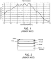
- Typical quantum efficiency (QE) curves of photodiodes look like the curve shown in FIG. 1 . What is actually not immediately apparent from this representation is that it is based on the light being collected over a wide angle range, as well as with limited spectral resolution, so it does not reveal the other drawback, which is caused by the interference effects of the underlying structure.
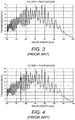
- FIG. 2 The structure of a typical photo-diode is shown in FIG. 2 .
- the thin dielectric layers SiO 2 and Si 3 N 4 as shown
- the quantum efficiency curve looks like the graph in FIG. 3 .
- the curve in FIG. 3 converts to the curve in FIG. 1 . This is due to two effects: a) an averaging that occurs when lowering the spectral resolution; and b) a wavelength-shift of the spectral response with angle.
- a typical diode is used with a broad-band light source, or with broad-band filters (e.g., dye based color filters), or at large acceptance angles, the principal drawback is a lower overall transmission level. This can be compensated for by using larger diodes. However, increasing the size of the diode is not always the most desirable solution.
- FIG. 4 shows an overlay of the transmission curve for a narrow bandpass filter (at approx. 540 nm) with the response of a standard photodiode, such as shown in FIG. 3 .
- the total throughput in the passband can vary by more than a factor of 2.
- the bandpass filter transmits at 900 nm, the throughput is only 30%, where a filter transmitting at 770 nm may see an almost 100% transmittal.
- Another drawback is that the locations of the ripples in the transmission curve of the photodiode are not well controlled. Thus, there can be a large variation of the photopic value from one device to another, because the spectral placement of the ripples may vary as a result of minor manufacturing inconsistencies or compositions of the materials.
- FIG. 5 An example is shown in FIG. 5 for a number of bandpass filters transmitting at a sequence of wavelengths, superimposed on the same photo-diode transmission curve as shown in FIGS. 3 and 4 .
- the overall transmission at a given bandpass filter wavelength varies dramatically from one wavelength to the next, depending on how the peaks align with the ripples in the photodiode transmission spectrum.
- first and second as used herein are not intended to denote any particular order or placement of an element. Instead, these terms are used herein to denote that one element differs from another element. As used herein, the terms “approximately” and “about” indicate a range of values within +/- 5% of a stated value.
- Disclosed herein is a method of fabricating sensor devices having optical filters that may be used in conjunction with back illuminated sensors.
- Devices having optical filters in conjunction with back illuminated sensors will have application to many types of sensor, particularly those used in multi- and hyper- spectral imaging and sensing.
- reflectors and mirrors or mirrored layers are used interchangeably.
- BIS 10 may include a silicon p/n junction layer 12.
- the p/n junction 12 may be formed from dopants in the silicon, close to the interface with the silicon p/n junction layer 12.
- a stack of dielectric layers 14, which may be formed of SiO 2 may be formed on one side of the silicon p/n junction layer 12.
- another dielectric layer 16, which may be Si 3 N 4 may be formed on an opposite side of the stack of dielectric layers 14.
- Metal contact layers 18 may be situated within the layers of the stack of dielectric layers 14. Light may enter the BIS 10 into the silicon p/n junction layer 12 without first passing through any of the dielectric layers 14, 16.
- the thickness of the stack of dielectric layers 14 may be adjusted according to the light that is desired to pass through the BIS 10. This means that, when combining with a bandpass function, it may only be necessary to match the optical filter frequency to the refractive index profile of the "substrate" medium 12, which may be silicon. Thus, interference artefacts that typically arise from the light passing through dielectric layers such as oxide and nitride are non-existent with this approach.
- the sensor device 100 is depicted as including a substrate 102 and a plurality of sensing elements 104.
- the substrate 102 may be formed of a passive material, such as silicon, glass, or the like.
- One or more of the sensing elements 104 may be a photodiode, a complementary metal-oxide semiconductor (CMOS), a charge-coupled device (CCD), or the like.
- CMOS complementary metal-oxide semiconductor
- CCD charge-coupled device
- the sensor device 100 is depicted as including a 4x4 array of sensing elements 104. It should, however, be clearly understood that the sensor device 100 may include any number of sensing elements 104.
- the sensor device 100 may include a first mirror layer 106 formed on one side of the substrate 102 such that the first mirror layer 106 extends over each of the sensing elements 104.
- the sensor device 100 may also include a base spacer layer 110, a first spacer layer 112, a second spacer layer 114, and a second mirror layer 116.
- the sensor device 100 may include additional spacer layers positioned above various ones of the sensing elements 104 and between the first mirror layer 106 and the second mirror layer 116.
- Various manners in which the sensor device 100 may be fabricated are described with respect to the following figures.
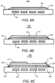
- FIGS. 8A-8E there are collectively shown an example method 200 of fabricating the sensor device 100 depicted in FIGS. 7A and 7B .
- a first mirror layer 106 is formed on a substrate 102, in which the substrate 102 includes an array of sensing elements 104.
- the first mirror layer 106 may be formed of a metallic material such as silver, aluminum, copper, gold, or the like.
- the first mirror layer 106 may be formed via a metal deposition process such as, magnetron sputtering, electron beam epitaxy, molecular beam epitaxy, thermal evaporation, atomic layer deposition, or the like.
- the first mirror layer 106 may be formed with tapered edges 108 due to the deposition process and a lift-off process. That is, each of the edges of the first mirror layer 106 may be tapered due to a combination of the deposition process and a lift-off process, e.g., a photo-resist having an overhang may be used during the deposition and lift-off processes, which may produce the tapered edges 108.
- the first mirror layer 106 may be formed to have a ZnO/Ag/ZnO structure, in which the ZnO thickness is between about 0.5 nm to about 4 nm. In other example, the ZnO thickness may be between about 1 nm to about 2 nm.
- the first mirror layer 106 may be formed of a dielectric material such as SiO 2 , NbO 2 , or the like. In further examples, the first mirror layer 106 may be formed of quarter-wave stacks, for instance, of SiO 2 and Si:H layers. In still further examples, the first mirror layer 106 may be formed of oxides, nitrides, Ge, Si, Si:H, SiC, or the like. Examples of suitable oxides include high index: Nb 2 O 5 Ta 2 O 5 , TiO 2 , HfO 2 , and mixtures thereof and low index: SiO 2 , Al 2 O 3 , and mixtures thereof.
- the first mirror layer 106 is formed of Si:H or SiO 2 . In these examples, the first mirror layer 106 may not be formed with the tapered edges.
- a base spacer layer 110 may be deposited on the first mirror layer 106 to cover the first mirror layer 106, including the tapered edges 108, if present.
- the base spacer layer 110 may be formed of materials such as oxides, nitrides, Ge, Si, Si:H, SiC, SiGe, SiGe:H or the like.
- the base spacer layer 110 may be formed of the same or similar materials as those discussed above with respect to the first mirror layer 106.
- the base spacer layer 110 is formed of Si:H.
- the base spacer layer 110 may be deposited during formation of the first mirror layer 106, e.g., in a common vacuum as the first mirror layer 106.
- the base spacer layer 110 may be deposited through performance of a suitable deposition process including any of chemical vapor deposition, physical vapor deposition, plasma-enhanced chemical vapor deposition, and the like.
- the base spacer layer 110 may be deposited using a lift-off process.
- deposition of the base spacer layer 110 may cause portions of the base spacer layer 110 to cover the tapered edges 108 of the first mirror layer 106.
- the base spacer layer 110 may be deposited to cover the tapered edges 108 of the first mirror layer 106 to protect the tapered edges 108 from oxidization, for example, in instances in which the first mirror layer 106 is formed of silver.
- the base spacer layer 110 may be deposited without covering the tapered edges 108.
- the base spacer layer 110 may include materials that perform additional filter functions such as anti-reflection, blocking, higher-order suppression filtering, or the like.
- an oxidizing preventing material layer such as a layer of zinc oxide (ZnO), may be provided below and above the first mirror layer 106 to further prevent the first mirror layer 106 from oxidizing.
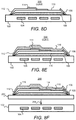
- a first spacer layer 112 may be deposited above a first group of sensing elements 104.
- the first spacer layer 112 may be deposited on the base spacer layer 110 above the eight sensing elements 104 located on the left side of the substrate 102.
- FIG. 9A depicts a top view of the configuration shown in FIG. 8C .
- the first spacer layer 112 may also be deposited to cover the tapered edges 108 of the first mirror layer 106.
- the portions of the base spacer layer 110 that are above the eight sensing elements 104 located on the right side of the substrate 102 may be uncovered by the first spacer layer 112, while the tapered edges 108 around the first mirror layer 106 are covered, as indicated by element 202.
- An enlarged cross-sectional side view of a portion of the configuration shown in FIG. 8C is depicted in FIG. 9B .
- the tapered edge 108 may be covered by a portion of the first spacer layer 110.
- the portion of the first spacer layer 110 that covers the tapered edge 108 may not provide sufficient protection to the tapered edge 108.
- a portion of the second spacer layer 112 may also be provided over the tapered edge 108.
- the top and the bottom of the tapered edge 108, as well as the remainder of the first mirror layer 106 may be covered by respective layers 115, 117 of oxidation preventing material, for instance, ZnO.
- the second mirror layer 116 may be similarly protected with the oxidation preventing material.
- the first spacer layer 112 may be deposited through implementation of similar deposition techniques as those discussed above with respect to the deposition of the base spacer layer 110.
- a mask (not shown) may be applied over the sections of the base spacer layer 110 that are not to receive the first spacer layer 112 during the deposition process to prevent the first spacer layer 112 from being deposited onto those sections.
- the mask may be removed following deposition of the first spacer layer 112.
- the mask may include a photoresist.
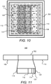
- a second spacer layer 114 may be deposited above a second group of sensing elements 104.
- the second spacer layer 114 may be deposited on part of the base spacer layer 110 above the four sensing elements 104 located on the middle-right side of the substrate 102 and on part of the first spacer layer 112 above the four sensing elements 104 located on the middle-left side of the substrate 102.
- FIG. 10 depicts a top view of the configuration shown in FIG. 8D .
- the heights or thicknesses of the spacer layers 110-114 above respective ones of the sensing elements 104 may differ for different groups of the sensing elements 104.
- different center wavelengths of light may be filtered prior to reaching the different groups of the sensing elements 104.
- the second spacer layer 114 may be deposited above half the sensing elements 104 as compared with the sensing elements 105 upon which the first spacer layer 112 was deposited.
- each subsequent spacer layer may deposited above half the sensing elements 104 as the previous spacer layer.
- each of the spacer layers 110-114 may have different heights (or thicknesses) with respect to each other.
- the base spacer layer 110 may be thicker than the first spacer layer 112 and the first spacer layer 112 may be thicker than the second spacer layer 114.
- subsequently deposited spacer layers (not shown), if deposited, may have increasingly smaller thicknesses.
- the second spacer layer 114 may be deposited through implementation of similar deposition techniques as those discussed above with respect to the deposition of the base spacer layer 110.
- a mask (not shown) may be applied over the sections of the base spacer layer 110 and the first spacer layer 112 that are not to receive the second spacer layer 114 during the deposition process to prevent the second spacer layer 114 from being deposited onto those sections. The mask may be removed following deposition of the second spacer layer 114.
- the areas above the tapered edges 108 of the first mirror layer 106 may be further covered by the second spacer layer 114.
- the second spacer layer 114 may be deposited over the tapered edges 108 of the first mirror layer 106 and on top of the portions 202 of the first spacer layer 112 that cover the tapered edges 108.
- a second mirror layer 116 may be formed above the deposited spacer layers 110-114.
- the second mirror layer 116 may be formed of a metallic material such as silver, aluminum, or the like.
- the second mirror layer 116 may be formed of a dielectric material such as SiO 2 , NbO 2 , or the like.
- the second mirror layer 116 may be formed of quarter-wave stacks, for instance, of SiO 2 and Si:H layers.
- the second mirror layer 116 may be formed in any of the manners discussed above with respect to formation of the first mirror layer 106. Deposition of the second mirror layer 116 may also include the addition of materials that may perform extra filter functions such as anti-reflection, out of band blocking, higher-order suppression filtering, or the like.
- additional processing may be performed, such as, the addition of micro lenses (not shown) to the second mirror layer 116.
- the method 200 of fabricating the sensor device 100 has been described as including two spacer layers 112 and 114, it should be understood that the method 200 may include additional spacer layer deposition steps. By way of particular example, the method 200 may include six spacer layer deposition steps such that many different filter structures may be fabricated over the sensing elements 104.
- FIG. 8F there is shown an example of a method of fabricating the sensor device 100 according to another example.
- FIG. 8F includes many of the same features as those discussed above with respect to FIGS. 8A-8E and thus, those common features are not described in detail with respect to FIG. 8F .
- the example shown in FIG. 8F differs from the example shown in FIG. 8E in that the mirror layers 106, 116 and the spacer layers 110-114 are formed on a substrate 252 that may not include sensing elements. That is, instead of being formed on the substrate 102, which includes an array of sensing elements 104, the example in FIG.
- the mirror layers 106, 116 and the spacer layers 110-114 maybe formed on a separate substrate 252, which may be a glass wafer.
- the substrate 252 may be adhered to the substrate 102, which may be a sensor array, as indicated by the arrow 254.
- the substrate 252 may be adhered to the substrate 102 through use of an epoxy and more particularly, a transparent epoxy.
- the sensor device 100 may be a single cavity Fabry-Perot filter.
- the center wavelengths of light that are filtered by the filter may vary depending the thickness of the spacer in the cavity.
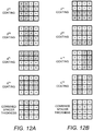
- FIG. 11 depicts an example structure 300 for a binary filter, for instance, a single cavity Fabry-Perot filter, which may represent a portion of the sensor device 100, e.g., a portion above a particular sensing element 104, according to an example.
- a cavity 302 is provided between the first mirror layer 106 and the second mirror layer 116.
- the structure 300 shows the relationship between the size of the spacer layers in the cavity 302 and the channel (e.g., center wavelength) that is filtered by the spacer layers. It has been observed that relatively small differences in spacer thickness may result in a significant separation of center wavelengths between otherwise identical filters.
- the filter may filter the 0 th channel, e.g., the filter may filter light having a first center wavelength.
- the filter may filter the 8 th channel.
- the filter may filter the 4 th channel.
- the filter may filter the 2 nd channel.
- the filter may filter the 1 st channel.
- a determination may be made as to how the filters are to be configured for each of the sensing elements 104. That is, the channels (e.g., center wavelengths of light) that the filters are to filter for each of the sensing elements 104 may be determined. In addition, based upon the correlation between the filtering of the channels and the thicknesses of the spacer layer in the cavity 302, the corresponding arrangement of the spacer layer depositions over the respective sensing elements 104 may be determined. For example, a determination may be made that a first group of sensing elements 104, which may be a single sensing element, is to filter the 4 th channel.
- the channels e.g., center wavelengths of light
- a determination may be made that the base spacer layer 110 and the first spacer layer 112 are to be deposited over the second group of sensing elements 104.
- the number of coating runs e.g., the number of spacer layers that are to be deposited for a filter array based on a binary filter structure
- c 2 n coat ⁇ 2 ⁇ b
- n coat log 2 c + 2 + b
- “c” represents the channel number
- "n coat” represents the number of coating runs
- “b” represents the number of additional AR coatings or blockers for higher order suppression. The additional blockers are described in greater detail herein below.
- Equations (3)-(5) “c” is the channel number, "t 0 " is the thickness of the base spacer layer 110, “t 1 " is the thickness of the first spacer layer 112, and “t n “ is the thickness of the last spacer layer 122.
- ⁇ min " is the lowest center wavelength, “ ⁇ max " is the highest center wavelength, and "n ref " is the refractive index of the spacer layer.
- any number of channels may be realized through implementation of the methods disclosed herein.
- the methods disclosed herein may be used for 100 channels, although the same number of coating runs for 128 channels would be required.
- the methods disclosed herein may be used for 50 channels, although the same number of coating runs for 64 channels would be required.
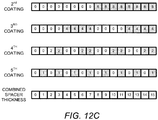
- FIGS. 12A-12C there are shown example filter arrays based on a binary filter structure. More particularly, each of FIGS. 12A-12C depicts the thickness of a spacer layer, as a multiple of a unit thickness, deposited during each of several coating runs.
- the spacer layers are shown as initially being deposited during a second coating run because the first coating run may include the deposition of the base spacer layer.
- the thicknesses of the respective spacer layers vary by a binary number. That is, the thickness of each of the spacer layers decreases by a factor of two during each of the coating runs.
- filter arrays depicted in FIGS. 12A-12C have equidistant channel spacing.
- the thicknesses of the spacer layers may be determined through Equations (3)-(5) discussed above.
- the thickness of each of the spacer layers may vary by different factors.
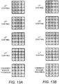
- the filter array may have a binary filter structure with non-equidistant channel spacing. Two examples of these types of 16 channel filter arrays are shown in FIGS. 13A and 13B . These types of filter arrays may be employed when channels may be skipped, which may result in the non-equidistant channel spacing.
- FIG. 14 there is shown an example structure 400, shown in cross-section, for a binary filter using dielectric reflectors/mirrors, which may represent a portion of the sensor device 100, e.g., a portion above a particular sensing element 104, according to an example.
- the structure 400 may be formed of alternating layers of materials, for instance, SiO 2 402 and Si:H 404 on a substrate 102.
- a spacer 406 may have a minimum thickness of 108.5 nm and may be made up of up to 6 spacer layers. Together, groups of the layers function as visible blockers 408 and reflectors 410, 412.
- the layers 402 and 404 in a reflector 410 may be quarter wave stacks, i.e., form a reflector at that wavelength.
- the layers 402 and 404 in a reflector 412 may also be quarter wave stacks.
- the total thickness of the structure may be in the range of about 1732 nm to about 1782.5 nm.
- the visible blockers 408 and the reflectors 410, 412 may each have a thickness of about 1160 nm.
- the base spacer layer 110 may have a thickness of between about 80 nm to about 130 nm
- the first spacer layer 112 may have a thickness of between about 10 nm to about 50 nm
- the second spacer layer 114 may have a thickness of between about 5 nm to about 25 nm
- the third spacer layer 120 may have a thickness of between about 2.5 nm to about 13 nm
- the fourth spacer layer 122 may have a thickness of between about 1.5 nm to about 7 nm.
- the thinnest thickness that a layer may have may be less than 1 nm, for instance, about 0.6 nm in the case of 128 channels.
- FIG. 15 there are shown example structures 500, shown in cross-section, for a binary filter using metal reflectors/mirrors, which may represent a portion of the sensor device 100, e.g., a portion above a particular sensing element 104, according to an example.
- the structures 500 may include an Ag based single-cavity Fabry-Perot functioning in UV-Vis-NIR.
- the upper structure shows a portion of a filter for UV-green channels and the lower structure shows a portion of a filter for green-NIR channels.
- the filter for UV-green channels is depicted as including an anti-reflective (AR) coating 502, which may be formed of NbTiOx, SiO 2 , or the like.
- the AR coating 502 may have a thickness of about 140 nm.
- the AR coating 502 may protect the mirror layer as well as provide anti-reflection properties.
- the lower structure shows a portion of a filter for green-NIR channels.
- Each of the structures 500 may include a first order spacer 504, which may be similar to the spacer 406 depicted in FIG. 14 .
- the spacer 504 may be up to around 150 nm thin and may be sandwiched between two mirror layers 506, which may be around 45 nm thick and may be formed of Ag.
- the lower structure may also include a UV-green blocker 508, which may be around 3000 nm thick and may be composed of alternating layers of NbTiOx and SiO 2 .
- the blocker 508 may suppress higher order peaks as discussed in greater detail herein below with respect to FIG. 16 .
- FIG. 16 shows a spectral response of the structures 500 depicted in FIG. 15 , according to an example.
- the blocker 508 suppresses higher order peaks at lower wavelengths.
- the blocker 508 may be implemented when a large spectral bandwidth is to be covered.
- light is to be transmitted at 850 nm, which may require the addition of a longwave pass that blocks the higher order peaks at 350 nm and 450 nm.
- the blocker is depicted in FIG. 16 as reference numeral 602.
- the spectral response of the Fabry-Perot filter made from the substrate 102, the first and second mirror layer 506, and the spacer 504 is depicted in FIG. 16 as reference numeral 604.
- FIG. 17 there is shown an enlarged diagram of an 8x8 filter array that may be fabricated through implementation of the methods disclosed herein. As shown in that figure, a pattern is repeated every 8 pixels.
Landscapes
- Physics & Mathematics (AREA)
- Spectroscopy & Molecular Physics (AREA)
- General Physics & Mathematics (AREA)
- Optics & Photonics (AREA)
- Optical Filters (AREA)
- Spectrometry And Color Measurement (AREA)
- Solid State Image Pick-Up Elements (AREA)
- Light Receiving Elements (AREA)
Applications Claiming Priority (1)
| Application Number | Priority Date | Filing Date | Title |
|---|---|---|---|
| US201662294982P | 2016-02-12 | 2016-02-12 |
Publications (1)
| Publication Number | Publication Date |
|---|---|
| EP3246949A1 true EP3246949A1 (fr) | 2017-11-22 |
Family
ID=58094165
Family Applications (1)
| Application Number | Title | Priority Date | Filing Date |
|---|---|---|---|
| EP17154949.6A Withdrawn EP3246949A1 (fr) | 2016-02-12 | 2017-02-07 | Procédé de fabrication d'un dispositif capteur |
Country Status (7)
| Country | Link |
|---|---|
| US (1) | US20170234726A1 (fr) |
| EP (1) | EP3246949A1 (fr) |
| JP (1) | JP2017168822A (fr) |
| KR (3) | KR20170095157A (fr) |
| CN (1) | CN107086224A (fr) |
| CA (1) | CA2957193C (fr) |
| TW (1) | TWI706549B (fr) |
Families Citing this family (11)
| Publication number | Priority date | Publication date | Assignee | Title |
|---|---|---|---|---|
| CN106331442B (zh) * | 2015-07-02 | 2021-01-15 | 松下知识产权经营株式会社 | 摄像装置 |
| US11231533B2 (en) | 2018-07-12 | 2022-01-25 | Visera Technologies Company Limited | Optical element having dielectric layers formed by ion-assisted deposition and method for fabricating the same |
| US11143803B2 (en) | 2018-07-30 | 2021-10-12 | Viavi Solutions Inc. | Multispectral filter |
| US10962694B2 (en) * | 2018-11-02 | 2021-03-30 | Viavi Solutions Inc. | Stepped structure optical filter |
| EP3913341A4 (fr) | 2019-01-16 | 2022-02-23 | Panasonic Intellectual Property Management Co., Ltd. | Filtre optique, dispositif de photodétection et système de photodétection |
| JP6952294B2 (ja) | 2019-01-16 | 2021-10-20 | パナソニックIpマネジメント株式会社 | 光検出装置、光検出システム、およびフィルタアレイ |
| WO2020180174A1 (fr) * | 2019-03-07 | 2020-09-10 | Technische Universiteit Eindhoven | Capteur spectral à pixels multiples |
| US11081600B2 (en) * | 2019-05-10 | 2021-08-03 | Visera Technologies Company Limited | Light filter structure |
| US11789188B2 (en) * | 2019-07-19 | 2023-10-17 | Viavi Solutions Inc. | Optical filter |
| FR3118287B1 (fr) * | 2020-12-17 | 2022-12-02 | Commissariat Energie Atomique | Photodetecteur multispectral infrarouge |
| CN115980898B (zh) * | 2023-03-21 | 2023-06-20 | 成都沃达惠康科技股份有限公司 | 一种多元素多层中红外高反膜及其制备方法 |
Citations (4)
| Publication number | Priority date | Publication date | Assignee | Title |
|---|---|---|---|---|
| EP1592067A1 (fr) * | 2004-01-15 | 2005-11-02 | Matsushita Electric Industries Co., Ltd. | Dispositif d'imagerie a l'etat solide, procede de production dudit dispositif d'imagerie a l'etat solide et camera utilisant ledit dispositif |
| US20080042782A1 (en) * | 2005-04-27 | 2008-02-21 | Shanghai Institute Of Technical Physics, Chinese Academy Of Sciences | Integrated narrow bandpass filter array and a method for fabrication thereof |
| US20130240708A1 (en) * | 2012-03-14 | 2013-09-19 | Kabushiki Kaisha Toshiba | Solid-state image pickup device and method of manufacturing solid-state image pickup device |
| EP2746739A2 (fr) * | 2012-12-19 | 2014-06-25 | JDS Uniphase Corporation | Dispositif de détecteur comprenant un ou plusieurs filtres optiques métalliques-diélectriques |
Family Cites Families (10)
| Publication number | Priority date | Publication date | Assignee | Title |
|---|---|---|---|---|
| JPS6342429A (ja) * | 1986-08-08 | 1988-02-23 | Minolta Camera Co Ltd | 分光測定センサ |
| US4822998A (en) * | 1986-05-15 | 1989-04-18 | Minolta Camera Kabushiki Kaisha | Spectral sensor with interference filter |
| JP4111288B2 (ja) * | 1998-07-09 | 2008-07-02 | Tdk株式会社 | 波長選択型光検出器 |
| CN100487900C (zh) * | 2004-01-15 | 2009-05-13 | 松下电器产业株式会社 | 固体成像装置,其制造方法,和使用固体成像装置的相机 |
| JP2006215290A (ja) * | 2005-02-03 | 2006-08-17 | Sony Corp | 液晶表示用バックライト装置 |
| US8692198B2 (en) * | 2010-04-21 | 2014-04-08 | Sionyx, Inc. | Photosensitive imaging devices and associated methods |
| JP5754910B2 (ja) * | 2010-10-13 | 2015-07-29 | ローム株式会社 | 半導体装置 |
| US10197716B2 (en) * | 2012-12-19 | 2019-02-05 | Viavi Solutions Inc. | Metal-dielectric optical filter, sensor device, and fabrication method |
| JP5989810B2 (ja) * | 2013-02-07 | 2016-09-07 | シャープ株式会社 | 半導体装置およびその製造方法 |
| KR102273850B1 (ko) * | 2013-10-31 | 2021-07-05 | 하마마츠 포토닉스 가부시키가이샤 | 광검출 장치 |
-
2017
- 2017-02-03 JP JP2017018448A patent/JP2017168822A/ja active Pending
- 2017-02-06 CA CA2957193A patent/CA2957193C/fr active Active
- 2017-02-06 TW TW106103804A patent/TWI706549B/zh active
- 2017-02-07 EP EP17154949.6A patent/EP3246949A1/fr not_active Withdrawn
- 2017-02-10 KR KR1020170018976A patent/KR20170095157A/ko not_active Ceased
- 2017-02-10 US US15/429,616 patent/US20170234726A1/en not_active Abandoned
- 2017-02-13 CN CN201710075799.4A patent/CN107086224A/zh active Pending
-
2019
- 2019-05-08 KR KR1020190053821A patent/KR102097657B1/ko active Active
-
2020
- 2020-03-31 KR KR1020200039073A patent/KR102200622B1/ko active Active
Patent Citations (4)
| Publication number | Priority date | Publication date | Assignee | Title |
|---|---|---|---|---|
| EP1592067A1 (fr) * | 2004-01-15 | 2005-11-02 | Matsushita Electric Industries Co., Ltd. | Dispositif d'imagerie a l'etat solide, procede de production dudit dispositif d'imagerie a l'etat solide et camera utilisant ledit dispositif |
| US20080042782A1 (en) * | 2005-04-27 | 2008-02-21 | Shanghai Institute Of Technical Physics, Chinese Academy Of Sciences | Integrated narrow bandpass filter array and a method for fabrication thereof |
| US20130240708A1 (en) * | 2012-03-14 | 2013-09-19 | Kabushiki Kaisha Toshiba | Solid-state image pickup device and method of manufacturing solid-state image pickup device |
| EP2746739A2 (fr) * | 2012-12-19 | 2014-06-25 | JDS Uniphase Corporation | Dispositif de détecteur comprenant un ou plusieurs filtres optiques métalliques-diélectriques |
Non-Patent Citations (1)
| Title |
|---|
| LAPRAY ET AL.: "Multispectral Filter Arrays: Recent Advances and Practical Implementation", SENSORS, vol. 14, 2014, pages 21626 - 21659, XP055352092, DOI: doi:10.3390/s141121626 |
Also Published As
| Publication number | Publication date |
|---|---|
| CA2957193A1 (fr) | 2017-08-12 |
| KR20170095157A (ko) | 2017-08-22 |
| KR20190053157A (ko) | 2019-05-17 |
| TWI706549B (zh) | 2020-10-01 |
| KR102200622B1 (ko) | 2021-01-08 |
| TW201733098A (zh) | 2017-09-16 |
| JP2017168822A (ja) | 2017-09-21 |
| KR102097657B1 (ko) | 2020-04-06 |
| CN107086224A (zh) | 2017-08-22 |
| KR20200038214A (ko) | 2020-04-10 |
| US20170234726A1 (en) | 2017-08-17 |
| CA2957193C (fr) | 2022-06-28 |
Similar Documents
| Publication | Publication Date | Title |
|---|---|---|
| CA2957193C (fr) | Fabrication d'un dispositif capteur | |
| US20250204068A1 (en) | Optical filter array | |
| KR102956767B1 (ko) | 광학 센서 디바이스 및 디바이스 | |
| US7521666B2 (en) | Multi-cavity Fabry-Perot ambient light filter apparatus | |
| US8084728B2 (en) | Optical sensing device | |
| EP2746739A2 (fr) | Dispositif de détecteur comprenant un ou plusieurs filtres optiques métalliques-diélectriques | |
| US20130163005A1 (en) | Optical Sensing Device | |
| US8258456B2 (en) | Image sensor | |
| HK1243224A1 (en) | Method of fabricating a sensor device | |
| TWI919967B (zh) | 基於金屬鏡的多光譜濾光片陣列 | |
| HK1243183A1 (en) | Optical filter array |
Legal Events
| Date | Code | Title | Description |
|---|---|---|---|
| PUAI | Public reference made under article 153(3) epc to a published international application that has entered the european phase |
Free format text: ORIGINAL CODE: 0009012 |
|
| STAA | Information on the status of an ep patent application or granted ep patent |
Free format text: STATUS: THE APPLICATION HAS BEEN PUBLISHED |
|
| AK | Designated contracting states |
Kind code of ref document: A1 Designated state(s): AL AT BE BG CH CY CZ DE DK EE ES FI FR GB GR HR HU IE IS IT LI LT LU LV MC MK MT NL NO PL PT RO RS SE SI SK SM TR |
|
| AX | Request for extension of the european patent |
Extension state: BA ME |
|
| STAA | Information on the status of an ep patent application or granted ep patent |
Free format text: STATUS: REQUEST FOR EXAMINATION WAS MADE |
|
| 17P | Request for examination filed |
Effective date: 20180514 |
|
| RBV | Designated contracting states (corrected) |
Designated state(s): AL AT BE BG CH CY CZ DE DK EE ES FI FR GB GR HR HU IE IS IT LI LT LU LV MC MK MT NL NO PL PT RO RS SE SI SK SM TR |
|
| REG | Reference to a national code |
Ref country code: HK Ref legal event code: DE Ref document number: 1243224 Country of ref document: HK |
|
| RAP1 | Party data changed (applicant data changed or rights of an application transferred) |
Owner name: VIAVI SOLUTIONS INC. |
|
| STAA | Information on the status of an ep patent application or granted ep patent |
Free format text: STATUS: EXAMINATION IS IN PROGRESS |
|
| 17Q | First examination report despatched |
Effective date: 20200330 |
|
| STAA | Information on the status of an ep patent application or granted ep patent |
Free format text: STATUS: THE APPLICATION IS DEEMED TO BE WITHDRAWN |
|
| 18D | Application deemed to be withdrawn |
Effective date: 20210310 |
|
| REG | Reference to a national code |
Ref country code: HK Ref legal event code: WD Ref document number: 1243224 Country of ref document: HK |