EP3252812A2 - Eingebettete verpackungsstruktur - Google Patents
Eingebettete verpackungsstruktur Download PDFInfo
- Publication number
- EP3252812A2 EP3252812A2 EP17167076.3A EP17167076A EP3252812A2 EP 3252812 A2 EP3252812 A2 EP 3252812A2 EP 17167076 A EP17167076 A EP 17167076A EP 3252812 A2 EP3252812 A2 EP 3252812A2
- Authority
- EP
- European Patent Office
- Prior art keywords
- conductive
- layer
- conductive layer
- insulation material
- material layer
- Prior art date
- Legal status (The legal status is an assumption and is not a legal conclusion. Google has not performed a legal analysis and makes no representation as to the accuracy of the status listed.)
- Granted
Links
Images




Classifications
-
- H—ELECTRICITY
- H10—SEMICONDUCTOR DEVICES; ELECTRIC SOLID-STATE DEVICES NOT OTHERWISE PROVIDED FOR
- H10W—GENERIC PACKAGES, INTERCONNECTIONS, CONNECTORS OR OTHER CONSTRUCTIONAL DETAILS OF DEVICES COVERED BY CLASS H10
- H10W74/00—Encapsulations, e.g. protective coatings
- H10W74/10—Encapsulations, e.g. protective coatings characterised by their shape or disposition
- H10W74/111—Encapsulations, e.g. protective coatings characterised by their shape or disposition the semiconductor body being completely enclosed
-
- H—ELECTRICITY
- H05—ELECTRIC TECHNIQUES NOT OTHERWISE PROVIDED FOR
- H05K—PRINTED CIRCUITS; CASINGS OR CONSTRUCTIONAL DETAILS OF ELECTRIC APPARATUS; MANUFACTURE OF ASSEMBLAGES OF ELECTRICAL COMPONENTS
- H05K1/00—Printed circuits
- H05K1/18—Printed circuits structurally associated with non-printed electric components
- H05K1/182—Printed circuits structurally associated with non-printed electric components associated with components mounted in printed circuit boards [PCB], e.g. insert-mounted components [IMC]
- H05K1/185—Printed circuits structurally associated with non-printed electric components associated with components mounted in printed circuit boards [PCB], e.g. insert-mounted components [IMC] associated with components encapsulated in the insulating substrate of the PCBs; associated with components incorporated in internal layers of multilayer circuit boards
-
- H—ELECTRICITY
- H05—ELECTRIC TECHNIQUES NOT OTHERWISE PROVIDED FOR
- H05K—PRINTED CIRCUITS; CASINGS OR CONSTRUCTIONAL DETAILS OF ELECTRIC APPARATUS; MANUFACTURE OF ASSEMBLAGES OF ELECTRICAL COMPONENTS
- H05K1/00—Printed circuits
- H05K1/02—Details
- H05K1/11—Printed elements for providing electric connections to or between printed circuits
- H05K1/115—Via connections; Lands around holes or via connections
-
- H—ELECTRICITY
- H10—SEMICONDUCTOR DEVICES; ELECTRIC SOLID-STATE DEVICES NOT OTHERWISE PROVIDED FOR
- H10W—GENERIC PACKAGES, INTERCONNECTIONS, CONNECTORS OR OTHER CONSTRUCTIONAL DETAILS OF DEVICES COVERED BY CLASS H10
- H10W70/00—Package substrates; Interposers; Redistribution layers [RDL]
- H10W70/60—Insulating or insulated package substrates; Interposers; Redistribution layers
- H10W70/611—Insulating or insulated package substrates; Interposers; Redistribution layers for connecting multiple chips together
- H10W70/614—Insulating or insulated package substrates; Interposers; Redistribution layers for connecting multiple chips together the multiple chips being integrally enclosed
-
- H—ELECTRICITY
- H10—SEMICONDUCTOR DEVICES; ELECTRIC SOLID-STATE DEVICES NOT OTHERWISE PROVIDED FOR
- H10W—GENERIC PACKAGES, INTERCONNECTIONS, CONNECTORS OR OTHER CONSTRUCTIONAL DETAILS OF DEVICES COVERED BY CLASS H10
- H10W70/00—Package substrates; Interposers; Redistribution layers [RDL]
- H10W70/60—Insulating or insulated package substrates; Interposers; Redistribution layers
- H10W70/62—Insulating or insulated package substrates; Interposers; Redistribution layers characterised by their interconnections
- H10W70/65—Shapes or dispositions of interconnections
-
- H—ELECTRICITY
- H10—SEMICONDUCTOR DEVICES; ELECTRIC SOLID-STATE DEVICES NOT OTHERWISE PROVIDED FOR
- H10W—GENERIC PACKAGES, INTERCONNECTIONS, CONNECTORS OR OTHER CONSTRUCTIONAL DETAILS OF DEVICES COVERED BY CLASS H10
- H10W74/00—Encapsulations, e.g. protective coatings
- H10W74/10—Encapsulations, e.g. protective coatings characterised by their shape or disposition
- H10W74/111—Encapsulations, e.g. protective coatings characterised by their shape or disposition the semiconductor body being completely enclosed
- H10W74/114—Encapsulations, e.g. protective coatings characterised by their shape or disposition the semiconductor body being completely enclosed by a substrate and the encapsulations
-
- H—ELECTRICITY
- H10—SEMICONDUCTOR DEVICES; ELECTRIC SOLID-STATE DEVICES NOT OTHERWISE PROVIDED FOR
- H10W—GENERIC PACKAGES, INTERCONNECTIONS, CONNECTORS OR OTHER CONSTRUCTIONAL DETAILS OF DEVICES COVERED BY CLASS H10
- H10W90/00—Package configurations
- H10W90/701—Package configurations characterised by the relative positions of pads or connectors relative to package parts
-
- H—ELECTRICITY
- H05—ELECTRIC TECHNIQUES NOT OTHERWISE PROVIDED FOR
- H05K—PRINTED CIRCUITS; CASINGS OR CONSTRUCTIONAL DETAILS OF ELECTRIC APPARATUS; MANUFACTURE OF ASSEMBLAGES OF ELECTRICAL COMPONENTS
- H05K2201/00—Indexing scheme relating to printed circuits covered by H05K1/00
- H05K2201/10—Details of components or other objects attached to or integrated in a printed circuit board
- H05K2201/10007—Types of components
- H05K2201/10015—Non-printed capacitor
-
- H—ELECTRICITY
- H05—ELECTRIC TECHNIQUES NOT OTHERWISE PROVIDED FOR
- H05K—PRINTED CIRCUITS; CASINGS OR CONSTRUCTIONAL DETAILS OF ELECTRIC APPARATUS; MANUFACTURE OF ASSEMBLAGES OF ELECTRICAL COMPONENTS
- H05K2201/00—Indexing scheme relating to printed circuits covered by H05K1/00
- H05K2201/10—Details of components or other objects attached to or integrated in a printed circuit board
- H05K2201/10007—Types of components
- H05K2201/10022—Non-printed resistor
-
- H—ELECTRICITY
- H05—ELECTRIC TECHNIQUES NOT OTHERWISE PROVIDED FOR
- H05K—PRINTED CIRCUITS; CASINGS OR CONSTRUCTIONAL DETAILS OF ELECTRIC APPARATUS; MANUFACTURE OF ASSEMBLAGES OF ELECTRICAL COMPONENTS
- H05K2201/00—Indexing scheme relating to printed circuits covered by H05K1/00
- H05K2201/10—Details of components or other objects attached to or integrated in a printed circuit board
- H05K2201/10007—Types of components
- H05K2201/1003—Non-printed inductor
-
- H—ELECTRICITY
- H10—SEMICONDUCTOR DEVICES; ELECTRIC SOLID-STATE DEVICES NOT OTHERWISE PROVIDED FOR
- H10W—GENERIC PACKAGES, INTERCONNECTIONS, CONNECTORS OR OTHER CONSTRUCTIONAL DETAILS OF DEVICES COVERED BY CLASS H10
- H10W70/00—Package substrates; Interposers; Redistribution layers [RDL]
- H10W70/01—Manufacture or treatment
- H10W70/05—Manufacture or treatment of insulating or insulated package substrates, or of interposers, or of redistribution layers
- H10W70/08—Manufacture or treatment of insulating or insulated package substrates, or of interposers, or of redistribution layers by depositing layers on the chip or wafer, e.g. "chip-first" RDLs
- H10W70/09—Manufacture or treatment of insulating or insulated package substrates, or of interposers, or of redistribution layers by depositing layers on the chip or wafer, e.g. "chip-first" RDLs extending onto an encapsulation that laterally surrounds the chip or wafer, e.g. fan-out wafer level package [FOWLP] RDLs
-
- H—ELECTRICITY
- H10—SEMICONDUCTOR DEVICES; ELECTRIC SOLID-STATE DEVICES NOT OTHERWISE PROVIDED FOR
- H10W—GENERIC PACKAGES, INTERCONNECTIONS, CONNECTORS OR OTHER CONSTRUCTIONAL DETAILS OF DEVICES COVERED BY CLASS H10
- H10W70/00—Package substrates; Interposers; Redistribution layers [RDL]
- H10W70/60—Insulating or insulated package substrates; Interposers; Redistribution layers
-
- H—ELECTRICITY
- H10—SEMICONDUCTOR DEVICES; ELECTRIC SOLID-STATE DEVICES NOT OTHERWISE PROVIDED FOR
- H10W—GENERIC PACKAGES, INTERCONNECTIONS, CONNECTORS OR OTHER CONSTRUCTIONAL DETAILS OF DEVICES COVERED BY CLASS H10
- H10W72/00—Interconnections or connectors in packages
- H10W72/90—Bond pads, in general
- H10W72/921—Structures or relative sizes of bond pads
- H10W72/926—Multiple bond pads having different sizes
-
- H—ELECTRICITY
- H10—SEMICONDUCTOR DEVICES; ELECTRIC SOLID-STATE DEVICES NOT OTHERWISE PROVIDED FOR
- H10W—GENERIC PACKAGES, INTERCONNECTIONS, CONNECTORS OR OTHER CONSTRUCTIONAL DETAILS OF DEVICES COVERED BY CLASS H10
- H10W72/00—Interconnections or connectors in packages
- H10W72/90—Bond pads, in general
- H10W72/941—Dispositions of bond pads
- H10W72/9413—Dispositions of bond pads on encapsulations
-
- H—ELECTRICITY
- H10—SEMICONDUCTOR DEVICES; ELECTRIC SOLID-STATE DEVICES NOT OTHERWISE PROVIDED FOR
- H10W—GENERIC PACKAGES, INTERCONNECTIONS, CONNECTORS OR OTHER CONSTRUCTIONAL DETAILS OF DEVICES COVERED BY CLASS H10
- H10W72/00—Interconnections or connectors in packages
- H10W72/90—Bond pads, in general
- H10W72/941—Dispositions of bond pads
- H10W72/944—Dispositions of multiple bond pads
-
- H—ELECTRICITY
- H10—SEMICONDUCTOR DEVICES; ELECTRIC SOLID-STATE DEVICES NOT OTHERWISE PROVIDED FOR
- H10W—GENERIC PACKAGES, INTERCONNECTIONS, CONNECTORS OR OTHER CONSTRUCTIONAL DETAILS OF DEVICES COVERED BY CLASS H10
- H10W90/00—Package configurations
Definitions
- the present invention relates to a package structure, and more particularly to an embedded package structure.
- a power module is one of the widely-used circuit modules.
- An example of the power module includes but is not limited to a DC-to-DC converter, a DC-to-AC converter or an AC-to-DC converter.
- the power module may be installed on a motherboard or a system circuit board.
- an embedded package structure is widely adopted.
- the process of fabricating the conventional embedded package structure will be illustrated as follows. Firstly, an electronic component with at least one conducting terminal (e.g., an active component) is embedded within an insulation substrate. Then, at least one via is formed in the insulation substrate by a laser drilling process. After a conductive material is filled in the via, a conductive via is formed. Then, a conductive layer is formed on the insulation substrate and contacted with the conductive via. Then, a passive component is installed on the above structure, and the passive component is electrically connected with the electronic component. Since the passive component and the electronic component are electrically connected with each other through the conductive layer and the conductive via, the passive component and the electronic component are vertically arranged in a stack form. Under this circumstance, the layout area of the motherboard or the system circuit board is saved.
- the passive component, the electronic component and the conductive layer are arranged in the stack form, the overall thickness of the embedded package structure is large (e.g., larger than 1000 micrometer).
- the conventional embedded package structure is not suitable for an ultra-thin electronic product (e.g., a smart watch or a tablet computer).
- An embedded package structure according to the present invention has an electronic component and a passive component separately and horizontally embedded within an insulation substrate. Consequently, the overall thickness of the embedded package structure is reduced, and the embedded package structure is suitably applied to the ultra-thin electronic product.
- the embedded package structure according to the present invention also enables a slim and easily fabricated package structure. Moreover, the embedded package structure has high power density, good electrical properties and good heat management performance.
- an embedded package structure includes an insulation substrate, a first conductive layer, a second conductive layer, an electronic component, a first insulation material layer, a second insulation material layer and a passive component.
- the insulation substrate has at least one first conductive via and at least one second conductive via.
- the first conductive layer is formed on a top surface of the insulation substrate.
- the first conductive layer is in contact with the at least first conductive via.
- the second conductive layer is formed on a bottom surface of the insulation substrate.
- the second conductive layer is in contact with the at least second conductive via.
- the electronic component is embedded within the insulation substrate, and includes plural first conducting terminals.
- the plural first conducting terminals are electrically connected with the first conductive layer and the second conductive layer through the at least one first conductive via and the at least one second conductive via, respectively.
- the first insulation material layer is formed on an outer surface of the first conductive layer and a part of the top surface of the insulation substrate.
- the second insulation material layer is formed on an outer surface of the second conductive layer and a part of the bottom surface of the insulation substrate.
- the passive component is located near a first side of the electronic component and separated from the electronic component. The passive component is at least partially embedded within the insulation substrate.
- an embedded package structure in accordance with another aspect of the present invention, there is provided an embedded package structure.
- the embedded package structure includes a dielectric substrate, an electronic component, at least a first redistribution layer, a passive component, and a second redistribution layer.
- the dielectric substrate has a first region and a second region adjacent to the first region.
- the electronic component is embedded within the first region of the dielectric substrate.
- the at least one first redistribution layer is formed within the first region of the dielectric substrate and electrically connected to the electronic component.
- the passive component is embedded within the dielectric substrate and at least partially disposed within the second region of the dielectric substrate.
- the second redistribution layer is disposed on a surface of the dielectric substrate, and the second redistribution layer is located in the first region and the second region and electrically connected with the passive component and the electronic component.
- a thickness of the passive component is larger than that of the electronic component.
- FIG. 1 is a schematic cross-sectional view illustrating an embedded package structure according to a first embodiment of the present invention.
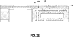
- FIGS. 2A to 2E are schematic cross-sectional views illustrating a fabricating process of the embedded package structure of FIG. 1 .
- the embedded package structure 1 comprises an insulation substrate 10, an electronic component 11, a first conductive layer 12, a second conductive layer 13, a first insulation material layer 14a, a second insulation material layer 14b and a passive component 15.
- the electronic component 11 is embedded within the insulation substrate 10, and the electronic component 11 comprises plural first conducting terminals 110.
- plural conductive vias 103 and plural conductive vias 104 are formed in the insulation substrate 10.
- the first conductive layer 12 is formed on a top surface 101 of the insulation substrate 10. In addition, the top surface 101 of the insulation substrate 10 is partially exposed through the first conductive layer 12. The first conductive layer 12 is in contact with the plural conductive vias 103.
- the second conductive layer 13 is formed on a bottom surface 102 of the insulation substrate 10. In addition, the bottom surface 102 of the insulation substrate 10 is partially exposed through the second conductive layer 13. The second conductive layer 13 is in contact with the plural conductive vias 104.
- the first conducting terminals 110 on a top surface 111 of the electronic component 11 are in contact with the corresponding conductive vias 103.
- the first conducting terminal 110 on a bottom surface 112 of the electronic component 11 is in contact with the corresponding conductive vias 104.
- the electronic component 11 is electrically connected with the first conductive layer 12 and the second conductive layer 13 through the plural first conducting terminals 110, the plural conductive vias 103 and the plural conductive vias 104.
- the first insulation material layer 14a is formed on an outer surface 12a of the first conductive layer 12 and a part of the top surface 101 of the insulation substrate 10.
- the second insulation material layer 14b is formed on an outer surface 13a of the second conductive layer 13 and a part of the bottom surface 102 of the insulation substrate 10.
- the passive component 15 is separated from the electronic component 11 and located beside the electronic component 11 along a horizontal direction. Moreover, at least a part of the passive component 15 is embedded within the insulation substrate 10.
- the passive component 15 has one or more second conducting terminals 150.
- the embedded package structure 1 further comprises an opening 15a.
- the opening 15a is located beside the electronic component 11.
- the opening 15a runs through the first insulation material layer 14a, the second insulation material layer 14b and the insulation substrate 10. At least a part of the passive component 15 is accommodated within the opening 15a. Consequently, the passive component 15 is separated from the electronic component 11 though the first insulation material layer 14a, the second insulation material layer 14b and the insulation substrate 10.
- the opening 15a is formed after the portions of the first insulation material layer 14a, the second insulation material layer 14b and the insulation substrate 10 beside the electronic component 11 are removed by a laser drilling process.
- the opening 15a is larger than the passive component 15.
- the passive component 15 is accommodated within the opening 15a, a gap is formed between the passive component 15 and an inner surface of the opening 15a.
- the passive component 15 is at least partially embedded within the first insulation material layer 14a, the second insulation material layer 14b and the insulation substrate 10.
- the embedded package structure 1 further comprises a fixing structure 16, a third conductive layer 17, a fourth conductive layer 18, plural conductive edges 10c and a groove 19.
- the third conductive layer 17 is formed on a top surface 141 of the first insulation material layer 14a.
- the top surface 141 of the first insulation material layer 14a is partially exposed through the third conductive layer 17.
- the fixing structure 16 is formed on the top surface 141 of the first insulation material layer 14a, an outer surface 17a of the third conductive layer 17 and an outer surface 155 of the passive component 15, and filled in the gap between the passive component 15 and the inner surface of the opening 15a.
- the first insulation material layer 14a, the third conductive layer 17 and the passive component 15 are combined together through the fixing structure 16.
- the passive component 15 is securely fixed in the opening 15a through the fixing structure 16.
- plural conductive channels 106 are formed in the fixing structure 16.
- the plural conductive channels 106 are in contact with the top surface 17a of the third conductive layer 17 and the second conducting terminals 150 of the passive component 15.
- the fourth conductive layer 18 is formed on a top surface 161 of the fixing structure 16.
- the fourth conductive layer 18 is in contact with the top surface of the plural conductive channels 106, and the top surface 161 of the fixing structure 16 is partially exposed through the fourth conductive layer 18.
- plural conductive vias 105 are formed in the first insulation material layer 14a.
- the first ends of the conductive vias 105 are in contact with the outer surface 12a of the first conductive layer 12.
- the second ends of the conductive vias 105 are in contact with a bottom surface of the third conductive layer 17.
- the first conducting terminals 110 on the top surface 111 of the electronic component 11 are electrically connected with the corresponding conductive vias 105 through the conductive vias 103.
- the groove 19 is arranged between the passive component 15 and the electronic component 11.
- the groove 19 is formed by a laser drilling process.
- the groove 19 has a first wall 10a and a second wall 10b, wherein the first wall and the second wall 10b are opposed to each other.
- the embedded package structure 1 further comprises a third insulation material layer 14c.
- the third insulation material layer 14c is filled in the groove 19, and contacted with the first insulation material layer 14a and the second insulation material layer 14b.
- the plural conductive edges 10c are formed on the first wall 10a and the second wall 10b, and contacted with the first conductive layer 12 and the second conductive layer 13. Due to the groove 19, the isolation between the passive component 15 and the electronic component 11 is enhanced.
- one or more separate first conductive blocks, one or more separate second conductive blocks, one or more separate third conductive blocks and one or more fourth conductive blocks are formed by etching the first conductive layer 12, the second conductive layer 13, the third conductive layer 17 and the fourth conductive layer 18.
- the first conductive blocks of the first conductive layer 12 are in contact with the corresponding conductive vias 103 and the corresponding conductive vias 105.
- the second conductive blocks of the second conductive layer 13 are in contact with the corresponding conductive vias 104.
- the third conductive blocks of the third conductive layer 17 are in contact with the corresponding conductive vias 105 and the corresponding conductive channels 106.
- the fourth conductive blocks of the fourth conductive layer 18 are in contact with the corresponding conductive channels 106.
- the first conductive layer 12, the second conductive layer 13, the third conductive layer 17 and the fourth conductive layer 18 are made of copper or any other appropriate conductive material.
- the first conductive layer 12, the second conductive layer 13, the third conductive layer 17 and the fourth conductive layer 18 are formed by an electroplating process or a depositing process.
- the conductive vias 103 are formed in the insulation substrate 10, exposed to the top surface 101 of the insulation substrate 10, and contacted with the first conductive layer 12.
- the conductive vias 104 are formed in the insulation substrate 10, exposed to the bottom surface 102 of the insulation substrate 10, and contacted with the second conductive layer 13.
- the plural conductive vias 103 and the plural conductive vias 104 are formed.
- the conductive vias 105 are formed in the first insulation material layer 14a, exposed to the top surface 141 of the first insulation material layer 14a, and contacted with the third conductive layer 17.
- the method of forming the conductive vias 105 is similar to the method of forming the conductive vias 103 and the conductive vias 104, and is not redundantly described herein.
- the insulation substrate 10 is made of prepreg material or any other appropriate insulation material with high thermal conductivity.
- the first insulation material layer 14a, the second insulation material layer 14b and the third insulation material layer 14c are made of solder mask material, and the fixing structure 16 is made of one or more insulation materials, such as a solder mask material.
- the electronic component 11 is an active component.
- An example of the electronic component 11 includes but is not limited to an integrated circuit (IC) chip, an integrated power component, a metal-oxide-semiconductor field-effect transistor (MOSFET), an insulated-gate bipolar transistor (IGBT).
- the electronic component 11 is arranged between the plural conductive vias 103 and the plural conductive vias 104.
- the first conducting terminals 110 on the top surface 111 of the electronic component 11 are electrically connected with the corresponding first conductive blocks of the first conductive layer 12 through the corresponding conductive vias 103.
- the first conducting terminal 110 on the bottom surface 112 of the electronic component 11 are electrically connected with the corresponding second conductive blocks of the second conductive layer 13 through the corresponding conductive vias 104.
- An example of the passive component 15 includes but is not limited to a capacitor, a resistor or an inductor.
- the passive component 15 comprises a choke.
- the first conducting terminals 150 of the passive component 15 are electrically connected with the corresponding fourth conductive blocks of the fourth conductive layer 18 through the corresponding conductive channels.
- the conductive vias 105 and the third conductive layer 17 are collaboratively formed as a re-distribution layer (RDL), and the conductive channels 106 and the fourth conductive layer 18 are collaboratively formed as another re-distribution layer (RDL).
- the fourth conductive blocks of the fourth conductive layer 18 may be served as contact pads. Consequently, the embedded package structure can be electrically connected with a system circuit board (not shown) through the contact pads.
- the embedded package structure 1 includes a dielectric substrate, an electronic component 11, at least a first redistribution layer, a passive component 15, and a second redistribution layer.
- the dielectric substrate has a first region and a second region adjacent to the first region.
- the dielectric substrate comprises an insulation substrate 10, a first insulation material layer 14a, a second insulation material layer 14b and a fixing structure 16.
- the electronic component 11 is embedded within the first region of the dielectric substrate.
- the at least one first redistribution layer is formed within the first region of the dielectric substrate and electrically connected to the electronic component 11.
- the passive component 15 is embedded within the dielectric substrate and at least partially disposed within the second region of the dielectric substrate.
- the second redistribution layer is disposed on a surface of the dielectric substrate, and the second redistribution layer is located in the first region and the second region and electrically connected with the passive component 15 and the electronic component 11.
- a thickness of the passive component 15 is larger than that of the electronic component 11.
- FIGS. 2A to 2E a process of fabricating a package structure of the embedded package structure 1 of FIG. 1 will be illustrated with reference to FIGS. 2A to 2E .
- a semi-package unit of the embedded package structure 1 is provided.
- the electronic component 11 is embedded within the insulation substrate 10.
- the plural first vias 103 are in contact with the corresponding first conductive blocks of the first conductive layer 12 on the top surface 101 of the insulation substrate 10, and the plural second vias 104 are in contact with the corresponding second conductive blocks of the second conductive layer 13 on the bottom surface 102 of the insulation substrate 10.
- the first insulation material layer 14a is formed on a part of the top surface 101 of the insulation substrate 10 and the outer surface 12a of the first conductive layer 12, and the second insulation material layer 14b is formed on a part of the bottom surface 102 of the insulation substrate 10 and the outer surface 13a of the second conductive layer 13.
- the plural conductive vias 105 are formed in the first insulation material layer 14a and contacted with the corresponding first conductive blocks of the first conductive layer 12.
- the third conductive layer 17 is formed on the top surface 141 of the first insulation material layer 14a, wherein the corresponding third conductive blocks of the third conductive layer 17 are contacted with the corresponding third vias 105.
- the opening 15a is formed in the first insulation material layer 14a, the insulation substrate 10 and the second insulation material layer 14b.
- the opening 15a is formed by a laser drilling process.
- the passive component 15 is placed within the opening 15a.
- the passive component 15 is placed within the opening 15a and attached on the thermal tape 15b.
- the fixing structure 16 is formed on the top surface 141 of the first insulation material layer 14a, the outer surface 17a of the third conductive layer 17 and the outer surface 155 of the passive component 15, and filled in the gap between the passive component 15 and the inner surface of the opening 15a. Since the passive component 15 is encapsulated by the fixing structure 16, the passive component 15 is securely fixed within the opening 15a. Then, the thermal tape 15b is removed.
- the fourth conductive layer 18 is formed on the top surface 161 of the fixing structure 16 and contacted with the corresponding conductive channels 106. Consequently, the embedded package structure 1 as shown in FIG. 1 is fabricated.
- FIG. 3 is a schematic cross-sectional view illustrating an embedded package structure according to a second embodiment of the present invention.
- the passive component 15 of the embedded package structure 3 of this embodiment is completely accommodated within the opening 15a.
- the outer surface 155 of the passive component 15 is at the same level with the top surface of the first insulation material layer 14a, and the second conductive terminals 150 of the passive component 15 are in contact with the corresponding conductive channels 106.
- the conductive vias 105 is connected between the first conductive layer 12 and the corresponding conductive channel 106.
- the embedded package structure 3 comprises a fourth insulation material layer 14d, a magnetic element 15c and a fifth conductive layer 20, but does not comprise the third conductive layer 17 and the fourth conductive layer 18.
- the fourth insulation material layer 14d is formed on the top surface 161 of the fixing structure 16.
- the magnetic element 15c is embedded within the fourth insulation material layer 14d and disposed on the top surface 161 of the fixing structure 16.
- the fifth conductive layer 20 is formed on a top surface 143 of the fourth insulation material layer 14d.
- the top surface 143 of the fourth insulation material layer 14d is partially exposed through the fifth conductive layer 20.
- plural conductive vias 107 are formed in the fourth insulation material layer 14d.
- the first ends of the conductive vias 107 are in contact with the corresponding conductive channels 106 of the fixing structure 16.
- the second ends of the conductive vias 107 are in contact with the fifth conductive layer 20.
- the fifth conductive layer 20 is divided into one or more fifth conductive blocks by etching the fifth conductive layer 20.
- the fifth conductive blocks of the fifth conductive layer 20 are in contact with the second ends of the corresponding conductive vias 107.
- FIG. 4 is a schematic cross-sectional view illustrating an embedded package structure according to a third embodiment of the present invention.
- the passive component 15 of the embedded package structure 4 of this embodiment is completely embedded within the insulation substrate 10. Consequently, the fixing structure 16 is formed on the top surface 141 of the first insulation material layer 14a.
- plural conductive vias 108 are formed in the insulation substrate 10. The first ends of the plural conductive vias 108 are in contact with the first conductive layer 12.
- the passive component 15 comprises plural second conducting terminals 151.
- the plural second conducting terminals 151 are in contact with the second ends of the corresponding conductive vias 108.
- plural conductive vias 105 are formed in the first insulation material layer 14a.
- the conductive vias 105 are electrically connected with the corresponding conductive vias 108 through the first conductive layer 12.
- the embedded package structure 4 further comprises the fourth insulation material layer 14d, the magnetic element 15c and the fifth conductive layer 20, but does not comprise the third conductive layer 17 and the fourth conductive layer 18.
- the arrangements of the fourth insulation material layer 14d, the magnetic element 15c and the fifth conductive layer 20 of the embedded package structure 4 are similar to those of the embedded package structure 3 of the second embodiment.
- the thickness of the magnetic element 15c of the embedded package structure 4 is substantially equal to the thickness of the magnetic element 15c of the embedded package structure 3. However, the width of the magnetic element 15c of the embedded package structure 4 is wider than that of the magnetic element 15c of the embedded package structure 3.
- FIG. 5 is a schematic cross-sectional view illustrating an embedded package structure according to a fourth embodiment of the present invention.
- the passive component 15 of the embedded package structure 5 of this embodiment is directly formed by a semiconductor producing process.
- a capacitor 15d is formed in the insulation substrate 10 and a resistor R is formed on the insulation substrate 10 by the semiconductor producing process.
- the location and arrangement of the capacitor 15d are similar to those of the passive component 15 as shown in FIG. 4 .
- the resistor R is embedded within the first insulation material layer 14a and disposed on the top surface 101 of the insulation substrate 10.
- the conducting terminals of the resistor R are in contact with the corresponding conductive vias 105.
- the arrangements of the fourth insulation material layer 14d, the magnetic element 15c and the fifth conductive layer 20 of the embedded package structure 5 are similar to those of the embedded package structure 4 of the third embodiment.
- the overall thickness of the embedded package structure of the present invention is smaller than 1000 ⁇ m, preferably smaller than 800 ⁇ m, and the most preferably smaller than 600 ⁇ m Moreover, since the electronic component and the passive component are horizontally embedded within the insulation substrate, the heat dissipating efficacy is enhanced.
- the present invention provides an embedded package structure.
- An electronic component and a passive component are separately and horizontally embedded within an insulation substrate. Consequently, the overall thickness of the embedded package structure is reduced, and the embedded package structure is suitably applied to the ultra-thin electronic product.
- the package structure of the embedded package structure is slim and easily fabricated. Moreover, the embedded package structure has high power density, good electrical properties and good heat management performance.
Landscapes
- Engineering & Computer Science (AREA)
- Microelectronics & Electronic Packaging (AREA)
- Production Of Multi-Layered Print Wiring Board (AREA)
Applications Claiming Priority (1)
| Application Number | Priority Date | Filing Date | Title |
|---|---|---|---|
| SG10201604384YA SG10201604384YA (en) | 2016-05-31 | 2016-05-31 | Embedded package structure |
Publications (3)
| Publication Number | Publication Date |
|---|---|
| EP3252812A2 true EP3252812A2 (de) | 2017-12-06 |
| EP3252812A3 EP3252812A3 (de) | 2018-05-16 |
| EP3252812B1 EP3252812B1 (de) | 2021-01-13 |
Family
ID=58578907
Family Applications (1)
| Application Number | Title | Priority Date | Filing Date |
|---|---|---|---|
| EP17167076.3A Active EP3252812B1 (de) | 2016-05-31 | 2017-04-19 | Eingebettete verpackungsstruktur |
Country Status (4)
| Country | Link |
|---|---|
| US (1) | US9913380B2 (de) |
| EP (1) | EP3252812B1 (de) |
| CN (1) | CN107452694B (de) |
| SG (1) | SG10201604384YA (de) |
Cited By (1)
| Publication number | Priority date | Publication date | Assignee | Title |
|---|---|---|---|---|
| EP3716326A1 (de) * | 2019-03-25 | 2020-09-30 | Mitsubishi Electric R&D Centre Europe B.V. | Elektrische leistungsanordnung mit dicken elektrisch leitfähigen schichten |
Families Citing this family (14)
| Publication number | Priority date | Publication date | Assignee | Title |
|---|---|---|---|---|
| CN111106074B (zh) * | 2018-10-26 | 2022-04-08 | 台达电子企业管理(上海)有限公司 | 功率模块及其制造方法 |
| US10447166B2 (en) | 2015-08-31 | 2019-10-15 | Delta Electronics, Inc. | Power module |
| US11036269B2 (en) | 2014-09-02 | 2021-06-15 | Delta Electronics (Shanghai) Co., Ltd. | Power module and manufacturing method thereof |
| US20210081013A1 (en) | 2014-09-02 | 2021-03-18 | Delta Electronics, Inc. | Power supply apparatus |
| US10242973B2 (en) * | 2017-07-07 | 2019-03-26 | Samsung Electro-Mechanics Co., Ltd. | Fan-out-semiconductor package module |
| US10504865B2 (en) * | 2017-09-28 | 2019-12-10 | Taiwan Semiconductor Manufacturing Co., Ltd. | Package structure and method of manufacturing the same |
| KR101982056B1 (ko) * | 2017-10-31 | 2019-05-24 | 삼성전기주식회사 | 팬-아웃 반도체 패키지 모듈 |
| SG10201802515PA (en) * | 2018-03-27 | 2019-10-30 | Delta Electronics Int’L Singapore Pte Ltd | Packaging process |
| US11171070B2 (en) | 2018-06-21 | 2021-11-09 | At&S Austria Technologie & Systemtechnik Aktiengesellschaft | Component carrier with integrated thermally conductive cooling structures |
| KR102713129B1 (ko) | 2018-10-31 | 2024-10-07 | 삼성전자주식회사 | 반도체 패키지 및 이를 포함하는 안테나 모듈 |
| WO2020105542A1 (ja) * | 2018-11-19 | 2020-05-28 | ローム株式会社 | 半導体装置 |
| DE102018132143B4 (de) * | 2018-12-13 | 2023-10-12 | Infineon Technologies Ag | Leiterplatte, Chip-Kühlgehäuse, Baugruppe und Verfahren zum Kühlen eines Halbleiterchips |
| KR102547250B1 (ko) * | 2018-12-20 | 2023-06-23 | 삼성전자주식회사 | 반도체 패키지 |
| US12245377B2 (en) * | 2019-03-29 | 2025-03-04 | At&S Austria Technologie & Systemtechnik Aktiengesellschaft | Component carrier with embedded semiconductor component and embedded highly-conductive block which are mutually coupled |
Family Cites Families (18)
| Publication number | Priority date | Publication date | Assignee | Title |
|---|---|---|---|---|
| JP2001024312A (ja) | 1999-07-13 | 2001-01-26 | Taiyo Yuden Co Ltd | 電子装置の製造方法及び電子装置並びに樹脂充填方法 |
| JP4339739B2 (ja) | 2004-04-26 | 2009-10-07 | 太陽誘電株式会社 | 部品内蔵型多層基板 |
| TWI301739B (en) * | 2004-12-03 | 2008-10-01 | Via Tech Inc | Structure and method for embedded passive component assembly |
| KR100716815B1 (ko) | 2005-02-28 | 2007-05-09 | 삼성전기주식회사 | 칩 내장형 인쇄회로기판 및 그 제조방법 |
| US7572681B1 (en) | 2005-12-08 | 2009-08-11 | Amkor Technology, Inc. | Embedded electronic component package |
| US20080239685A1 (en) * | 2007-03-27 | 2008-10-02 | Tadahiko Kawabe | Capacitor built-in wiring board |
| JP4424449B2 (ja) | 2007-05-02 | 2010-03-03 | 株式会社村田製作所 | 部品内蔵モジュール及びその製造方法 |
| US8130507B2 (en) * | 2008-03-24 | 2012-03-06 | Ngk Spark Plug Co., Ltd. | Component built-in wiring board |
| WO2010050627A1 (ja) * | 2008-10-31 | 2010-05-06 | 太陽誘電株式会社 | プリント配線板およびその製造方法 |
| TWI446497B (zh) * | 2010-08-13 | 2014-07-21 | 欣興電子股份有限公司 | 嵌埋被動元件之封裝基板及其製法 |
| CN102751256B (zh) * | 2011-04-22 | 2015-10-14 | 欣兴电子股份有限公司 | 嵌埋被动组件的封装基板及其制造方法 |
| US9142426B2 (en) | 2011-06-20 | 2015-09-22 | Cyntec Co., Ltd. | Stack frame for electrical connections and the method to fabricate thereof |
| US10636735B2 (en) | 2011-10-14 | 2020-04-28 | Cyntec Co., Ltd. | Package structure and the method to fabricate thereof |
| TWI505755B (zh) * | 2012-04-13 | 2015-10-21 | 旭德科技股份有限公司 | 封裝載板及其製作方法 |
| KR101442347B1 (ko) * | 2012-11-15 | 2014-09-17 | 삼성전기주식회사 | 캐패시터 내장 기판 |
| US9345142B2 (en) | 2013-11-21 | 2016-05-17 | Samsung Electro-Mechanics Co., Ltd. | Chip embedded board and method of manufacturing the same |
| SG10201400396WA (en) | 2014-03-05 | 2015-10-29 | Delta Electronics Int’L Singapore Pte Ltd | Package structure and stacked package module with the same |
| SG10201401622RA (en) | 2014-04-17 | 2015-11-27 | Delta Electronics Int’L Singapore Pte Ltd | Package structure |
-
2016
- 2016-05-31 SG SG10201604384YA patent/SG10201604384YA/en unknown
-
2017
- 2017-04-01 CN CN201710212807.5A patent/CN107452694B/zh active Active
- 2017-04-18 US US15/490,178 patent/US9913380B2/en active Active
- 2017-04-19 EP EP17167076.3A patent/EP3252812B1/de active Active
Non-Patent Citations (1)
| Title |
|---|
| None |
Cited By (4)
| Publication number | Priority date | Publication date | Assignee | Title |
|---|---|---|---|---|
| EP3716326A1 (de) * | 2019-03-25 | 2020-09-30 | Mitsubishi Electric R&D Centre Europe B.V. | Elektrische leistungsanordnung mit dicken elektrisch leitfähigen schichten |
| WO2020195089A1 (en) * | 2019-03-25 | 2020-10-01 | Mitsubishi Electric Corporation | Electrically power assembly with thick electrically conductive layers |
| JP2022515931A (ja) * | 2019-03-25 | 2022-02-22 | ミツビシ・エレクトリック・アールアンドディー・センター・ヨーロッパ・ビーヴィ | 厚い導電層を備える電気パワーアセンブリ |
| US11791254B2 (en) | 2019-03-25 | 2023-10-17 | Mitsubishi Electric Corporation | Electrically power assembly with thick electrically conductive layers |
Also Published As
| Publication number | Publication date |
|---|---|
| CN107452694B (zh) | 2020-08-21 |
| CN107452694A (zh) | 2017-12-08 |
| EP3252812B1 (de) | 2021-01-13 |
| SG10201604384YA (en) | 2017-12-28 |
| US9913380B2 (en) | 2018-03-06 |
| US20170347458A1 (en) | 2017-11-30 |
| EP3252812A3 (de) | 2018-05-16 |
Similar Documents
| Publication | Publication Date | Title |
|---|---|---|
| EP3252812B1 (de) | Eingebettete verpackungsstruktur | |
| US9425131B2 (en) | Package structure | |
| US9107290B1 (en) | Package structure and stacked package module with the same | |
| US12058814B2 (en) | Power module and manufacturing method thereof | |
| US9287231B2 (en) | Package structure with direct bond copper substrate | |
| US7875498B2 (en) | Chip module for complete power train | |
| US10219390B2 (en) | Fabrication method of packaging substrate having embedded passive component | |
| US7754538B2 (en) | Packaging substrate structure with electronic components embedded therein and method for manufacturing the same | |
| US20200152557A1 (en) | Package structure and packaging process | |
| US8619428B2 (en) | Electronic package structure | |
| US20170025379A1 (en) | Power module package | |
| US10573614B2 (en) | Process for fabricating a circuit substrate | |
| US20190043799A1 (en) | Package structure and fabricating method thereof | |
| EP3547353B1 (de) | Verpackungsverfahren | |
| US10083925B2 (en) | Packaging process of electronic component | |
| US11277067B2 (en) | Power module and manufacturing method thereof | |
| US10412821B1 (en) | Dual side cooling structure | |
| US11711893B2 (en) | Electronic component, voltage regulation module and voltage stabilizer | |
| US20260026400A1 (en) | High density device package and packaging technique thereof | |
| KR20250145495A (ko) | 회로기판 및 이를 포함하는 반도체 패키지 |
Legal Events
| Date | Code | Title | Description |
|---|---|---|---|
| PUAI | Public reference made under article 153(3) epc to a published international application that has entered the european phase |
Free format text: ORIGINAL CODE: 0009012 |
|
| STAA | Information on the status of an ep patent application or granted ep patent |
Free format text: STATUS: THE APPLICATION HAS BEEN PUBLISHED |
|
| AK | Designated contracting states |
Kind code of ref document: A2 Designated state(s): AL AT BE BG CH CY CZ DE DK EE ES FI FR GB GR HR HU IE IS IT LI LT LU LV MC MK MT NL NO PL PT RO RS SE SI SK SM TR |
|
| AX | Request for extension of the european patent |
Extension state: BA ME |
|
| RIC1 | Information provided on ipc code assigned before grant |
Ipc: H01L 23/538 20060101AFI20171212BHEP |
|
| PUAL | Search report despatched |
Free format text: ORIGINAL CODE: 0009013 |
|
| AK | Designated contracting states |
Kind code of ref document: A3 Designated state(s): AL AT BE BG CH CY CZ DE DK EE ES FI FR GB GR HR HU IE IS IT LI LT LU LV MC MK MT NL NO PL PT RO RS SE SI SK SM TR |
|
| AX | Request for extension of the european patent |
Extension state: BA ME |
|
| RIC1 | Information provided on ipc code assigned before grant |
Ipc: H01L 23/538 20060101AFI20180411BHEP |
|
| STAA | Information on the status of an ep patent application or granted ep patent |
Free format text: STATUS: REQUEST FOR EXAMINATION WAS MADE |
|
| 17P | Request for examination filed |
Effective date: 20181115 |
|
| RBV | Designated contracting states (corrected) |
Designated state(s): AL AT BE BG CH CY CZ DE DK EE ES FI FR GB GR HR HU IE IS IT LI LT LU LV MC MK MT NL NO PL PT RO RS SE SI SK SM TR |
|
| GRAP | Despatch of communication of intention to grant a patent |
Free format text: ORIGINAL CODE: EPIDOSNIGR1 |
|
| STAA | Information on the status of an ep patent application or granted ep patent |
Free format text: STATUS: GRANT OF PATENT IS INTENDED |
|
| INTG | Intention to grant announced |
Effective date: 20200908 |
|
| GRAJ | Information related to disapproval of communication of intention to grant by the applicant or resumption of examination proceedings by the epo deleted |
Free format text: ORIGINAL CODE: EPIDOSDIGR1 |
|
| STAA | Information on the status of an ep patent application or granted ep patent |
Free format text: STATUS: REQUEST FOR EXAMINATION WAS MADE |
|
| GRAR | Information related to intention to grant a patent recorded |
Free format text: ORIGINAL CODE: EPIDOSNIGR71 |
|
| GRAS | Grant fee paid |
Free format text: ORIGINAL CODE: EPIDOSNIGR3 |
|
| STAA | Information on the status of an ep patent application or granted ep patent |
Free format text: STATUS: GRANT OF PATENT IS INTENDED |
|
| INTC | Intention to grant announced (deleted) | ||
| GRAA | (expected) grant |
Free format text: ORIGINAL CODE: 0009210 |
|
| STAA | Information on the status of an ep patent application or granted ep patent |
Free format text: STATUS: THE PATENT HAS BEEN GRANTED |
|
| AK | Designated contracting states |
Kind code of ref document: B1 Designated state(s): AL AT BE BG CH CY CZ DE DK EE ES FI FR GB GR HR HU IE IS IT LI LT LU LV MC MK MT NL NO PL PT RO RS SE SI SK SM TR |
|
| INTG | Intention to grant announced |
Effective date: 20201207 |
|
| REG | Reference to a national code |
Ref country code: GB Ref legal event code: FG4D |
|
| REG | Reference to a national code |
Ref country code: CH Ref legal event code: EP |
|
| REG | Reference to a national code |
Ref country code: DE Ref legal event code: R096 Ref document number: 602017031266 Country of ref document: DE |
|
| REG | Reference to a national code |
Ref country code: IE Ref legal event code: FG4D |
|
| REG | Reference to a national code |
Ref country code: AT Ref legal event code: REF Ref document number: 1355182 Country of ref document: AT Kind code of ref document: T Effective date: 20210215 |
|
| REG | Reference to a national code |
Ref country code: AT Ref legal event code: MK05 Ref document number: 1355182 Country of ref document: AT Kind code of ref document: T Effective date: 20210113 |
|
| REG | Reference to a national code |
Ref country code: NL Ref legal event code: MP Effective date: 20210113 |
|
| REG | Reference to a national code |
Ref country code: LT Ref legal event code: MG9D |
|
| PG25 | Lapsed in a contracting state [announced via postgrant information from national office to epo] |
Ref country code: BG Free format text: LAPSE BECAUSE OF FAILURE TO SUBMIT A TRANSLATION OF THE DESCRIPTION OR TO PAY THE FEE WITHIN THE PRESCRIBED TIME-LIMIT Effective date: 20210413 Ref country code: LT Free format text: LAPSE BECAUSE OF FAILURE TO SUBMIT A TRANSLATION OF THE DESCRIPTION OR TO PAY THE FEE WITHIN THE PRESCRIBED TIME-LIMIT Effective date: 20210113 Ref country code: HR Free format text: LAPSE BECAUSE OF FAILURE TO SUBMIT A TRANSLATION OF THE DESCRIPTION OR TO PAY THE FEE WITHIN THE PRESCRIBED TIME-LIMIT Effective date: 20210113 Ref country code: GR Free format text: LAPSE BECAUSE OF FAILURE TO SUBMIT A TRANSLATION OF THE DESCRIPTION OR TO PAY THE FEE WITHIN THE PRESCRIBED TIME-LIMIT Effective date: 20210414 Ref country code: FI Free format text: LAPSE BECAUSE OF FAILURE TO SUBMIT A TRANSLATION OF THE DESCRIPTION OR TO PAY THE FEE WITHIN THE PRESCRIBED TIME-LIMIT Effective date: 20210113 Ref country code: PT Free format text: LAPSE BECAUSE OF FAILURE TO SUBMIT A TRANSLATION OF THE DESCRIPTION OR TO PAY THE FEE WITHIN THE PRESCRIBED TIME-LIMIT Effective date: 20210513 Ref country code: NO Free format text: LAPSE BECAUSE OF FAILURE TO SUBMIT A TRANSLATION OF THE DESCRIPTION OR TO PAY THE FEE WITHIN THE PRESCRIBED TIME-LIMIT Effective date: 20210413 |
|
| PG25 | Lapsed in a contracting state [announced via postgrant information from national office to epo] |
Ref country code: SE Free format text: LAPSE BECAUSE OF FAILURE TO SUBMIT A TRANSLATION OF THE DESCRIPTION OR TO PAY THE FEE WITHIN THE PRESCRIBED TIME-LIMIT Effective date: 20210113 Ref country code: AT Free format text: LAPSE BECAUSE OF FAILURE TO SUBMIT A TRANSLATION OF THE DESCRIPTION OR TO PAY THE FEE WITHIN THE PRESCRIBED TIME-LIMIT Effective date: 20210113 Ref country code: PL Free format text: LAPSE BECAUSE OF FAILURE TO SUBMIT A TRANSLATION OF THE DESCRIPTION OR TO PAY THE FEE WITHIN THE PRESCRIBED TIME-LIMIT Effective date: 20210113 Ref country code: RS Free format text: LAPSE BECAUSE OF FAILURE TO SUBMIT A TRANSLATION OF THE DESCRIPTION OR TO PAY THE FEE WITHIN THE PRESCRIBED TIME-LIMIT Effective date: 20210113 Ref country code: LV Free format text: LAPSE BECAUSE OF FAILURE TO SUBMIT A TRANSLATION OF THE DESCRIPTION OR TO PAY THE FEE WITHIN THE PRESCRIBED TIME-LIMIT Effective date: 20210113 |
|
| PG25 | Lapsed in a contracting state [announced via postgrant information from national office to epo] |
Ref country code: IS Free format text: LAPSE BECAUSE OF FAILURE TO SUBMIT A TRANSLATION OF THE DESCRIPTION OR TO PAY THE FEE WITHIN THE PRESCRIBED TIME-LIMIT Effective date: 20210513 |
|
| REG | Reference to a national code |
Ref country code: DE Ref legal event code: R097 Ref document number: 602017031266 Country of ref document: DE |
|
| PG25 | Lapsed in a contracting state [announced via postgrant information from national office to epo] |
Ref country code: SM Free format text: LAPSE BECAUSE OF FAILURE TO SUBMIT A TRANSLATION OF THE DESCRIPTION OR TO PAY THE FEE WITHIN THE PRESCRIBED TIME-LIMIT Effective date: 20210113 Ref country code: EE Free format text: LAPSE BECAUSE OF FAILURE TO SUBMIT A TRANSLATION OF THE DESCRIPTION OR TO PAY THE FEE WITHIN THE PRESCRIBED TIME-LIMIT Effective date: 20210113 Ref country code: CZ Free format text: LAPSE BECAUSE OF FAILURE TO SUBMIT A TRANSLATION OF THE DESCRIPTION OR TO PAY THE FEE WITHIN THE PRESCRIBED TIME-LIMIT Effective date: 20210113 |
|
| PLBE | No opposition filed within time limit |
Free format text: ORIGINAL CODE: 0009261 |
|
| STAA | Information on the status of an ep patent application or granted ep patent |
Free format text: STATUS: NO OPPOSITION FILED WITHIN TIME LIMIT |
|
| PG25 | Lapsed in a contracting state [announced via postgrant information from national office to epo] |
Ref country code: DK Free format text: LAPSE BECAUSE OF FAILURE TO SUBMIT A TRANSLATION OF THE DESCRIPTION OR TO PAY THE FEE WITHIN THE PRESCRIBED TIME-LIMIT Effective date: 20210113 Ref country code: MC Free format text: LAPSE BECAUSE OF FAILURE TO SUBMIT A TRANSLATION OF THE DESCRIPTION OR TO PAY THE FEE WITHIN THE PRESCRIBED TIME-LIMIT Effective date: 20210113 Ref country code: SK Free format text: LAPSE BECAUSE OF FAILURE TO SUBMIT A TRANSLATION OF THE DESCRIPTION OR TO PAY THE FEE WITHIN THE PRESCRIBED TIME-LIMIT Effective date: 20210113 Ref country code: RO Free format text: LAPSE BECAUSE OF FAILURE TO SUBMIT A TRANSLATION OF THE DESCRIPTION OR TO PAY THE FEE WITHIN THE PRESCRIBED TIME-LIMIT Effective date: 20210113 |
|
| 26N | No opposition filed |
Effective date: 20211014 |
|
| GBPC | Gb: european patent ceased through non-payment of renewal fee |
Effective date: 20210419 |
|
| PG25 | Lapsed in a contracting state [announced via postgrant information from national office to epo] |
Ref country code: LU Free format text: LAPSE BECAUSE OF NON-PAYMENT OF DUE FEES Effective date: 20210419 |
|
| REG | Reference to a national code |
Ref country code: BE Ref legal event code: MM Effective date: 20210430 |
|
| PG25 | Lapsed in a contracting state [announced via postgrant information from national office to epo] |
Ref country code: LI Free format text: LAPSE BECAUSE OF NON-PAYMENT OF DUE FEES Effective date: 20210430 Ref country code: AL Free format text: LAPSE BECAUSE OF FAILURE TO SUBMIT A TRANSLATION OF THE DESCRIPTION OR TO PAY THE FEE WITHIN THE PRESCRIBED TIME-LIMIT Effective date: 20210113 Ref country code: CH Free format text: LAPSE BECAUSE OF NON-PAYMENT OF DUE FEES Effective date: 20210430 Ref country code: GB Free format text: LAPSE BECAUSE OF NON-PAYMENT OF DUE FEES Effective date: 20210419 Ref country code: ES Free format text: LAPSE BECAUSE OF FAILURE TO SUBMIT A TRANSLATION OF THE DESCRIPTION OR TO PAY THE FEE WITHIN THE PRESCRIBED TIME-LIMIT Effective date: 20210113 |
|
| PG25 | Lapsed in a contracting state [announced via postgrant information from national office to epo] |
Ref country code: SI Free format text: LAPSE BECAUSE OF FAILURE TO SUBMIT A TRANSLATION OF THE DESCRIPTION OR TO PAY THE FEE WITHIN THE PRESCRIBED TIME-LIMIT Effective date: 20210113 |
|
| PG25 | Lapsed in a contracting state [announced via postgrant information from national office to epo] |
Ref country code: IT Free format text: LAPSE BECAUSE OF FAILURE TO SUBMIT A TRANSLATION OF THE DESCRIPTION OR TO PAY THE FEE WITHIN THE PRESCRIBED TIME-LIMIT Effective date: 20210113 Ref country code: IE Free format text: LAPSE BECAUSE OF NON-PAYMENT OF DUE FEES Effective date: 20210419 |
|
| PG25 | Lapsed in a contracting state [announced via postgrant information from national office to epo] |
Ref country code: IS Free format text: LAPSE BECAUSE OF FAILURE TO SUBMIT A TRANSLATION OF THE DESCRIPTION OR TO PAY THE FEE WITHIN THE PRESCRIBED TIME-LIMIT Effective date: 20210513 |
|
| PG25 | Lapsed in a contracting state [announced via postgrant information from national office to epo] |
Ref country code: BE Free format text: LAPSE BECAUSE OF NON-PAYMENT OF DUE FEES Effective date: 20210430 |
|
| PG25 | Lapsed in a contracting state [announced via postgrant information from national office to epo] |
Ref country code: HU Free format text: LAPSE BECAUSE OF FAILURE TO SUBMIT A TRANSLATION OF THE DESCRIPTION OR TO PAY THE FEE WITHIN THE PRESCRIBED TIME-LIMIT; INVALID AB INITIO Effective date: 20170419 |
|
| PG25 | Lapsed in a contracting state [announced via postgrant information from national office to epo] |
Ref country code: NL Free format text: LAPSE BECAUSE OF NON-PAYMENT OF DUE FEES Effective date: 20210113 Ref country code: CY Free format text: LAPSE BECAUSE OF FAILURE TO SUBMIT A TRANSLATION OF THE DESCRIPTION OR TO PAY THE FEE WITHIN THE PRESCRIBED TIME-LIMIT Effective date: 20210113 |
|
| PG25 | Lapsed in a contracting state [announced via postgrant information from national office to epo] |
Ref country code: MK Free format text: LAPSE BECAUSE OF FAILURE TO SUBMIT A TRANSLATION OF THE DESCRIPTION OR TO PAY THE FEE WITHIN THE PRESCRIBED TIME-LIMIT Effective date: 20210113 |
|
| PG25 | Lapsed in a contracting state [announced via postgrant information from national office to epo] |
Ref country code: MT Free format text: LAPSE BECAUSE OF FAILURE TO SUBMIT A TRANSLATION OF THE DESCRIPTION OR TO PAY THE FEE WITHIN THE PRESCRIBED TIME-LIMIT Effective date: 20210113 |
|
| PGFP | Annual fee paid to national office [announced via postgrant information from national office to epo] |
Ref country code: DE Payment date: 20250430 Year of fee payment: 9 |
|
| PGFP | Annual fee paid to national office [announced via postgrant information from national office to epo] |
Ref country code: FR Payment date: 20250430 Year of fee payment: 9 |
|
| REG | Reference to a national code |
Ref country code: DE Ref legal event code: R079 Ref document number: 602017031266 Country of ref document: DE Free format text: PREVIOUS MAIN CLASS: H01L0023538000 Ipc: H10W0070600000 |
|
| PG25 | Lapsed in a contracting state [announced via postgrant information from national office to epo] |
Ref country code: TR Free format text: LAPSE BECAUSE OF FAILURE TO SUBMIT A TRANSLATION OF THE DESCRIPTION OR TO PAY THE FEE WITHIN THE PRESCRIBED TIME-LIMIT Effective date: 20210113 |