EP3716326A1 - Elektrische leistungsanordnung mit dicken elektrisch leitfähigen schichten - Google Patents
Elektrische leistungsanordnung mit dicken elektrisch leitfähigen schichten Download PDFInfo
- Publication number
- EP3716326A1 EP3716326A1 EP19164827.8A EP19164827A EP3716326A1 EP 3716326 A1 EP3716326 A1 EP 3716326A1 EP 19164827 A EP19164827 A EP 19164827A EP 3716326 A1 EP3716326 A1 EP 3716326A1
- Authority
- EP
- European Patent Office
- Prior art keywords
- electrically conductive
- external
- conductive layer
- internal
- base structure
- Prior art date
- Legal status (The legal status is an assumption and is not a legal conclusion. Google has not performed a legal analysis and makes no representation as to the accuracy of the status listed.)
- Pending
Links
Images




Classifications
-
- H—ELECTRICITY
- H05—ELECTRIC TECHNIQUES NOT OTHERWISE PROVIDED FOR
- H05K—PRINTED CIRCUITS; CASINGS OR CONSTRUCTIONAL DETAILS OF ELECTRIC APPARATUS; MANUFACTURE OF ASSEMBLAGES OF ELECTRICAL COMPONENTS
- H05K1/00—Printed circuits
- H05K1/02—Details
- H05K1/0213—Electrical arrangements not otherwise provided for
- H05K1/0263—High current adaptations, e.g. printed high current conductors or using auxiliary non-printed means; Fine and coarse circuit patterns on one circuit board
-
- H—ELECTRICITY
- H10—SEMICONDUCTOR DEVICES; ELECTRIC SOLID-STATE DEVICES NOT OTHERWISE PROVIDED FOR
- H10W—GENERIC PACKAGES, INTERCONNECTIONS, CONNECTORS OR OTHER CONSTRUCTIONAL DETAILS OF DEVICES COVERED BY CLASS H10
- H10W70/00—Package substrates; Interposers; Redistribution layers [RDL]
- H10W70/60—Insulating or insulated package substrates; Interposers; Redistribution layers
- H10W70/62—Insulating or insulated package substrates; Interposers; Redistribution layers characterised by their interconnections
- H10W70/65—Shapes or dispositions of interconnections
- H10W70/658—Shapes or dispositions of interconnections for devices provided for in groups H10D8/00 - H10D48/00
-
- H—ELECTRICITY
- H05—ELECTRIC TECHNIQUES NOT OTHERWISE PROVIDED FOR
- H05K—PRINTED CIRCUITS; CASINGS OR CONSTRUCTIONAL DETAILS OF ELECTRIC APPARATUS; MANUFACTURE OF ASSEMBLAGES OF ELECTRICAL COMPONENTS
- H05K1/00—Printed circuits
- H05K1/18—Printed circuits structurally associated with non-printed electric components
- H05K1/182—Printed circuits structurally associated with non-printed electric components associated with components mounted in printed circuit boards [PCB], e.g. insert-mounted components [IMC]
- H05K1/185—Printed circuits structurally associated with non-printed electric components associated with components mounted in printed circuit boards [PCB], e.g. insert-mounted components [IMC] associated with components encapsulated in the insulating substrate of the PCBs; associated with components incorporated in internal layers of multilayer circuit boards
- H05K1/188—Printed circuits structurally associated with non-printed electric components associated with components mounted in printed circuit boards [PCB], e.g. insert-mounted components [IMC] associated with components encapsulated in the insulating substrate of the PCBs; associated with components incorporated in internal layers of multilayer circuit boards manufactured by mounting on or attaching to a structure having a conductive layer, e.g. a metal foil, such that the terminals of the component are connected to or adjacent to the conductive layer before embedding, and by using the conductive layer, which is patterned after embedding, at least partially for connecting the component
-
- H—ELECTRICITY
- H05—ELECTRIC TECHNIQUES NOT OTHERWISE PROVIDED FOR
- H05K—PRINTED CIRCUITS; CASINGS OR CONSTRUCTIONAL DETAILS OF ELECTRIC APPARATUS; MANUFACTURE OF ASSEMBLAGES OF ELECTRICAL COMPONENTS
- H05K3/00—Apparatus or processes for manufacturing printed circuits
- H05K3/46—Manufacturing multilayer circuits
- H05K3/4644—Manufacturing multilayer circuits by building the multilayer layer by layer, i.e. build-up multilayer circuits
- H05K3/4652—Adding a circuit layer by laminating a metal foil or a preformed metal foil pattern
-
- H—ELECTRICITY
- H10—SEMICONDUCTOR DEVICES; ELECTRIC SOLID-STATE DEVICES NOT OTHERWISE PROVIDED FOR
- H10W—GENERIC PACKAGES, INTERCONNECTIONS, CONNECTORS OR OTHER CONSTRUCTIONAL DETAILS OF DEVICES COVERED BY CLASS H10
- H10W70/00—Package substrates; Interposers; Redistribution layers [RDL]
- H10W70/01—Manufacture or treatment
- H10W70/05—Manufacture or treatment of insulating or insulated package substrates, or of interposers, or of redistribution layers
-
- H—ELECTRICITY
- H10—SEMICONDUCTOR DEVICES; ELECTRIC SOLID-STATE DEVICES NOT OTHERWISE PROVIDED FOR
- H10W—GENERIC PACKAGES, INTERCONNECTIONS, CONNECTORS OR OTHER CONSTRUCTIONAL DETAILS OF DEVICES COVERED BY CLASS H10
- H10W70/00—Package substrates; Interposers; Redistribution layers [RDL]
- H10W70/60—Insulating or insulated package substrates; Interposers; Redistribution layers
- H10W70/611—Insulating or insulated package substrates; Interposers; Redistribution layers for connecting multiple chips together
-
- H—ELECTRICITY
- H10—SEMICONDUCTOR DEVICES; ELECTRIC SOLID-STATE DEVICES NOT OTHERWISE PROVIDED FOR
- H10W—GENERIC PACKAGES, INTERCONNECTIONS, CONNECTORS OR OTHER CONSTRUCTIONAL DETAILS OF DEVICES COVERED BY CLASS H10
- H10W70/00—Package substrates; Interposers; Redistribution layers [RDL]
- H10W70/60—Insulating or insulated package substrates; Interposers; Redistribution layers
- H10W70/611—Insulating or insulated package substrates; Interposers; Redistribution layers for connecting multiple chips together
- H10W70/614—Insulating or insulated package substrates; Interposers; Redistribution layers for connecting multiple chips together the multiple chips being integrally enclosed
-
- H—ELECTRICITY
- H10—SEMICONDUCTOR DEVICES; ELECTRIC SOLID-STATE DEVICES NOT OTHERWISE PROVIDED FOR
- H10W—GENERIC PACKAGES, INTERCONNECTIONS, CONNECTORS OR OTHER CONSTRUCTIONAL DETAILS OF DEVICES COVERED BY CLASS H10
- H10W70/00—Package substrates; Interposers; Redistribution layers [RDL]
- H10W70/60—Insulating or insulated package substrates; Interposers; Redistribution layers
- H10W70/62—Insulating or insulated package substrates; Interposers; Redistribution layers characterised by their interconnections
- H10W70/63—Vias, e.g. via plugs
- H10W70/635—Through-vias
-
- H—ELECTRICITY
- H10—SEMICONDUCTOR DEVICES; ELECTRIC SOLID-STATE DEVICES NOT OTHERWISE PROVIDED FOR
- H10W—GENERIC PACKAGES, INTERCONNECTIONS, CONNECTORS OR OTHER CONSTRUCTIONAL DETAILS OF DEVICES COVERED BY CLASS H10
- H10W70/00—Package substrates; Interposers; Redistribution layers [RDL]
- H10W70/60—Insulating or insulated package substrates; Interposers; Redistribution layers
- H10W70/67—Insulating or insulated package substrates; Interposers; Redistribution layers characterised by their insulating layers or insulating parts
- H10W70/68—Shapes or dispositions thereof
-
- H—ELECTRICITY
- H10—SEMICONDUCTOR DEVICES; ELECTRIC SOLID-STATE DEVICES NOT OTHERWISE PROVIDED FOR
- H10W—GENERIC PACKAGES, INTERCONNECTIONS, CONNECTORS OR OTHER CONSTRUCTIONAL DETAILS OF DEVICES COVERED BY CLASS H10
- H10W70/00—Package substrates; Interposers; Redistribution layers [RDL]
- H10W70/60—Insulating or insulated package substrates; Interposers; Redistribution layers
- H10W70/67—Insulating or insulated package substrates; Interposers; Redistribution layers characterised by their insulating layers or insulating parts
- H10W70/68—Shapes or dispositions thereof
- H10W70/685—Shapes or dispositions thereof comprising multiple insulating layers
-
- H—ELECTRICITY
- H10—SEMICONDUCTOR DEVICES; ELECTRIC SOLID-STATE DEVICES NOT OTHERWISE PROVIDED FOR
- H10W—GENERIC PACKAGES, INTERCONNECTIONS, CONNECTORS OR OTHER CONSTRUCTIONAL DETAILS OF DEVICES COVERED BY CLASS H10
- H10W90/00—Package configurations
-
- H—ELECTRICITY
- H05—ELECTRIC TECHNIQUES NOT OTHERWISE PROVIDED FOR
- H05K—PRINTED CIRCUITS; CASINGS OR CONSTRUCTIONAL DETAILS OF ELECTRIC APPARATUS; MANUFACTURE OF ASSEMBLAGES OF ELECTRICAL COMPONENTS
- H05K2201/00—Indexing scheme relating to printed circuits covered by H05K1/00
- H05K2201/09—Shape and layout
- H05K2201/09209—Shape and layout details of conductors
- H05K2201/095—Conductive through-holes or vias
- H05K2201/09554—Via connected to metal substrate
-
- H—ELECTRICITY
- H05—ELECTRIC TECHNIQUES NOT OTHERWISE PROVIDED FOR
- H05K—PRINTED CIRCUITS; CASINGS OR CONSTRUCTIONAL DETAILS OF ELECTRIC APPARATUS; MANUFACTURE OF ASSEMBLAGES OF ELECTRICAL COMPONENTS
- H05K2201/00—Indexing scheme relating to printed circuits covered by H05K1/00
- H05K2201/10—Details of components or other objects attached to or integrated in a printed circuit board
- H05K2201/10007—Types of components
- H05K2201/10166—Transistor
-
- H—ELECTRICITY
- H05—ELECTRIC TECHNIQUES NOT OTHERWISE PROVIDED FOR
- H05K—PRINTED CIRCUITS; CASINGS OR CONSTRUCTIONAL DETAILS OF ELECTRIC APPARATUS; MANUFACTURE OF ASSEMBLAGES OF ELECTRICAL COMPONENTS
- H05K2203/00—Indexing scheme relating to apparatus or processes for manufacturing printed circuits covered by H05K3/00
- H05K2203/03—Metal processing
- H05K2203/0323—Working metal substrate or core, e.g. by etching, deforming
-
- H—ELECTRICITY
- H10—SEMICONDUCTOR DEVICES; ELECTRIC SOLID-STATE DEVICES NOT OTHERWISE PROVIDED FOR
- H10W—GENERIC PACKAGES, INTERCONNECTIONS, CONNECTORS OR OTHER CONSTRUCTIONAL DETAILS OF DEVICES COVERED BY CLASS H10
- H10W70/00—Package substrates; Interposers; Redistribution layers [RDL]
- H10W70/60—Insulating or insulated package substrates; Interposers; Redistribution layers
-
- H—ELECTRICITY
- H10—SEMICONDUCTOR DEVICES; ELECTRIC SOLID-STATE DEVICES NOT OTHERWISE PROVIDED FOR
- H10W—GENERIC PACKAGES, INTERCONNECTIONS, CONNECTORS OR OTHER CONSTRUCTIONAL DETAILS OF DEVICES COVERED BY CLASS H10
- H10W72/00—Interconnections or connectors in packages
- H10W72/90—Bond pads, in general
- H10W72/941—Dispositions of bond pads
- H10W72/9413—Dispositions of bond pads on encapsulations
-
- H—ELECTRICITY
- H10—SEMICONDUCTOR DEVICES; ELECTRIC SOLID-STATE DEVICES NOT OTHERWISE PROVIDED FOR
- H10W—GENERIC PACKAGES, INTERCONNECTIONS, CONNECTORS OR OTHER CONSTRUCTIONAL DETAILS OF DEVICES COVERED BY CLASS H10
- H10W72/00—Interconnections or connectors in packages
- H10W72/90—Bond pads, in general
- H10W72/941—Dispositions of bond pads
- H10W72/944—Dispositions of multiple bond pads
Definitions
- the invention relates to an electrically power assembly comprising at least one power device embedded in a multilayer base structure and at least one external thick electrically conductive layer providing better current and thermal transfer of the power device.
- the invention also relates to a manufacturing method of the power assembly.
- Power dies such as diodes or various types of power transistors (MOSFET, JFET, IGBT, HEMT) are elementary components of power modules which are used for the control and conversion of electric power, for instance in many different fields such as in the automotive, aeronautic, railway industries.
- DBC Direct Bonded Copper
- the constant increase in the switching frequency and density of power leads a need for thermal enhancement, volume reduction and reliability increase of the power modules.
- a new packaging technology is emerging which consists of manufacturing pre-packed power cells comprising at least one power die embedded in a Printed Circuit Board (PCB) laminate.
- the power dies are then connected to electrically conductive layers through plated vias.
- PCB Printed Circuit Board
- This new packaging solution allows easier connection of the power dies on a substrate.
- the connection by plated vias increases the reliability and reduces the parasitic elements of the interconnection.
- a conventional method for manufacturing a power device packaging comprises the following steps:
- the other solution is to obtain in first a thick external electrically layers before performing the step of drilling the vias.
- the invention aims at providing a power assembly with thick electrically conductive layers in order to increase the thermal and power capabilities of the power device.
- Another aim of the invention is to provide a power assembly which is easier to manufacture than in the prior art.
- a power assembly comprising:
- the power assembly according to the invention provides an enhanced power transmission thanks to the thick external conductive layers that are positioned on opposite sides of the multilayer base structure embedded the power device.
- said at least one multilayer base structure comprises:
- the thickness of the external layers is in a range of between 100 ⁇ m to 4 mm, and preferably 400 ⁇ m to 1 mm.
- the at least one hole has a ratio hole depth to pre-drilled hole diameter in range of between 0.4 to 1.6, and preferably 0.8 to 1.2.
- connections between an internal electrically conductive layer and an electrical contact of a power device are conductive vias.
- the diameter of the at least one hole is in a range of between 100 ⁇ m to 1500 ⁇ m.
- the at least one power device is a diode, a transistor such as a MOSFET, JFET or IGBT.
- a method for manufacturing a power assembly according to the above description comprising:
- the step of forming the multilayer base structure comprises:
- the method may comprise further steps wherein the sequence of steps (b) to (g) is repeated at least once.
- the sequence of steps (b) to (g) is repeated a number of times necessary to obtain a total thickness for the external conductive layers on each side of the base structure comprising between 1 mm and 100 mm.
- each external electrically conductive layer has a thickness in a range of between 100 ⁇ m to 4 mm, and preferably 400 ⁇ m to 1 mm.
- the at least one pre-drilled through hole of the external electrically conductive layers is pre-filled with a paste insulating material before positioning the external electrically conductive layers on each side of the base structure.
- the paste material is choosing among the group consisting of: epoxy resin, silicon.
- the at least one hole have a ratio vias hole depth to pre-drilled hole diameter ranging between 0.4 to 1.6, and preferably between 0.8 to 1.2.
- the power assembly according to the invention provides a good thermal dissipation and a high power transmission thanks to the thick external electrically conductive layers positioned on each side of the multilayer base structure.
- pre-drilled holes formed in the thick electrically conductive layers before lamination permits to drill the thick electrically conductive layers by mechanical process or any appropriate process and overcome the laser drilling limitation.
- electrical power assembly refers to a package structure comprising at least one power device embedded in a multilayer structure like a PCB laminate in order to form a power module.
- insulating layer or “insulating core” refers to a layer or core made of thermally conductive and electrically insulating material.
- conductive layer refers to a layer made of electrically and thermally conductive material.
- the power assembly 100 comprises an insulating core 30, in which is embedded a power device 20.
- the power device may be a diode or a MOSFET, a JFET or IGBT, HEMT.
- the power device is made from a wide bandgap semiconductor, i.e. a semiconductor having a bandgap in the range of 2-4 eV.
- the power device may be made in Silicon Carbide SiC or in Gallium Nitride GaN.
- the power device has at least two electrical contacts (not shown) which are metallic pads such as aluminum, gold, copper, silver etc.
- the power device is a diode and has two opposite electrical contacts.
- the power device is a transistor and has three electrical contacts comprising a gate, a source and a drain or a gate, an emitter and a collector, according to the type of transistor.
- the power device could also have a number of electrical contacts greater than three.
- the power assembly 100 may comprise at least one additional power device as shown in figure 2 and/or an electronic passive component such as a resistor, a capacitor, or other, connected to the first power device.
- an electronic passive component such as a resistor, a capacitor, or other
- the insulating core 30 is made of resin or any other appropriate insulating material with high thermal conductivity to provide better heat dissipation.
- the insulating core may be made of FR-4 glass epoxy, polyimide, or in ceramic such as HTCC (High-Temperature Co-Fired Ceramic) or LTCC (Low Temperature Co-fired Ceramic).
- the electrical power assembly 100 further comprises a top internal conductive layer 40 and a bottom internal conductive layer 40'.
- the top internal conductive layer 40 is disposed on a top surface 31 of the insulating core 30.
- the bottom internal conductive layer 40' is disposed on a bottom surface 31' of the insulating core 30.
- the material of these conductive layers is a metal, preferably copper.
- a set of top conductive vias 12 and a set of bottom vias 12' are formed in the insulating core 30 and in the top and bottom internal conductive layers 40, 40'.
- the contact pads of the top internal conductive layer 40 are connected to the electrical contacts on a top surface of the power device 20 by the set of top vias 12.
- the contact pads of the bottom internal conductive layer 40' are connected to the electrical contacts on a bottom surface of the power device by the set of bottom vias 12'.
- the power device 20 is therefore connected to the top internal conductive layer 40 and the bottom internal conductive layer 40' through the electrical pads, the set of top vias 12 and the set of bottom vias 12'.
- top vias 12 and the bottom vias 12' are well known to those skilled in the art. After laminating the stack up comprising the insulating core 30 and the two internal conductive layers 40, 40' in order to obtain a solid assembly, a set of bottom vias holes 11 and a set of bottom vias holes 11' are formed by laser drilling process at each side of the stack allowing the exposition of the electrical contacts of the power device 20. Then, the vias holes 11, 11' are filled with a conductive material such as copper by an electroplating process or electroless or both in order to form conductive vias 12, 12'.
- a conductive material such as copper by an electroplating process or electroless or both in order to form conductive vias 12, 12'.
- an etching step is applied on the surface of the top conductive layer 40 and the surface of the bottom conductive layer 40' in order to obtain respectively top conductive pattern and bottom conductive pattern. Therefore, the top conductive pattern and the bottom conductive pattern are served as the contact pads of the top internal conductive layer 40 and the bottom internal conductive layer 40'.
- the internal conductive layers 40, 40' may have a thickness of about 20-50 ⁇ m.
- the number of the vias is chosen according to the power transmission. These numbers depend also on the drilling technique, laser or mechanical.
- the density of vias connecting the electrical contact of the power device with the internal conductive layers may be at least 4 vias/mm 2 , for instance 15 vias/mm 2 , for instance with a ratio vias hole depth to drill diameter of 0.8.
- the power device is a MOSFET or IGBT, only one via connects the gate pad to the internal conductive layer.
- the package structure as described above forms an example of multilayer base structure 10 comprising the insulating core 30 and two thin internal conductive layers 40, 40' covering opposite surfaces of the insulating core 30, the insulating core 30 embedded at least one power device 20.
- the power assembly 100 further comprises a top thick external conductive layer 60 and a bottom thick external conductive layer, 60' positioned at each side of the base structure 10.
- the top and bottom thick external conductive layers have a thickness greater than the thickness of the internal conductive layers 40, 40' of the base structure in order to enhance the current and thermal capabilities of the package structure.
- the thick external conductive layers 60, 60' may have a thickness of about 100 ⁇ m-4mm, preferably about 400 ⁇ m-1mm.
- a thick layer is a layer having a thickness greater than or equal to 100 ⁇ m.
- the material of these layers is metal, preferably copper.
- each external thick electrically conductive layer 60, 60' comprises plural pre-drilled through holes 61, 61' which are formed by mechanical process or other such as an electroerosion. These predrilled through holes 61, 61' are served as conductive vias holes for connecting the external thick conductive layers 60, 60' to the contact pads of the internal conductive layers 40, 40' as will be explained in more detail below.
- the holes are formed in the thick conductive layers prior to positioning the thick layers in the stack for forming the power assembly, e.g. prior to the step of lamination of the stack. Therefore, there is no limitation on the drilling technique.
- the holes are formed by a mechanical drilling process in order to form deep holes.
- the pre-drilled through holes may have a hole diameter comprising between 100 ⁇ m and 1500 ⁇ m.
- these pre-drilled through holes 61, 61' are pre-filled with an insulating material by screen printing which will be removed later prior the step of electroplating process for forming conductive vias.
- the power assembly 100 further comprises a top internal insulating layer 50 and a bottom internal insulating layer 50', the top internal insulating layer 50 being disposed between the top external thick conductive layer 60 and the top internal thin electrically conductive layer 40 of the base structure 10 and the bottom internal insulating layer being 50' being disposed between the bottom external thick conductive layer 60' and the bottom internal conductive layer 40' of the base structure 10.
- the internal insulating layers 50, 50' are made of resin or any appropriate insulating material with high thermal conductivity.
- the epoxy resin present in the insulating layers 50, 50' flows and fill the pre-drilled through holes 61, 61' of the thick external conductive layers 60, 60'.
- the insulating material in the pre-drilled through holes and underneath the pre-drilled through holes is then removed in order to form holes 62, 62' extending from the internal conductive layers 40, 40' to the external surface 65, 65' of the external thick conductive layers 60, 60', through the internal insulating layers 50, 50'.
- the electrical power assembly 100 also comprises a set of top holes 62 extending from the top internal conductive layer 40, through the top insulating layer 50 and the top thick external electrically layer 60 and a set of bottom holes 62' extending from the bottom internal conductive layer 40', through the bottom insulating layer 50' and the bottom thick external electrically layer 60'.
- Each hole 62, 62' has a bottom 66, 66' and an open end 67, 67'.
- the bottom of the hole is formed by a portion of the contact pads of the internal conductive layers 40, 40' which are therefore exposed.
- the open end 67, 67' is formed at the surface 65, 65' of the external thick electrically conductive layer 60, 60'.
- Each hole 62, 62' is formed in part by a hole formed in the internal insulating layers 50, 50' and in part by the pre-drilled through hole 61, 61' formed in the external thick conductive layers 60, 60'.
- the holes 62, 62' have a ratio vias hole depth to pre-drilled diameter ranging between 0.4 to 1.6, and preferably between 0.8 to 1.2.
- the top and bottom holes 62, 62' are then filled with a conductive material 63 such as copper or a paste conductive material in order to form a set of top conductive vias 64 and a set of bottom conductive vias 64'.
- a conductive material 63 such as copper or a paste conductive material
- the holes may be fully filled with the conductive material from the bottom of the holes until the surface of the external thick conductive layer.
- the holes 62, 62' are plated by a conductive material.
- the assembly is dipped into two baths, the first being copper electroless plating in order to connect the internal conductive layers to the external conductive layers, a second being an electroplating bath in order to fully fill the holes 62, 62'.
- the contact pads of the top internal conductive layer 40 are connected to the external thick conductive layer 60 by the top vias 64 arranged in the top internal insulating layer 50 and in the top external conductive layer 60.
- the contact pads of the bottom internal conductive layer 40' are connected to the bottom external thick conductive layer 60' by the bottom vias 64' arranged in the bottom internal insulating layer 50' and in the bottom external conductive layer 60'.
- the power device 20 is electrically connected with the top external thick conductive layer 60 and the bottom external thick conductive layer 60'.
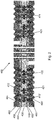
- FIG. 2 is a schematic cross-sectional view illustrating an electrical power assembly 400 according to a second embodiment of the present invention.
- the electrical power assembly comprises plural power devices, for instance four power devices 421, 422, 423 and 424 as shown in figure 2 .
- the power devices may same or different with each other.
- the number of the electrical contacts of each power device is determined according to the type of the power device.
- the power assembly comprises two diodes and two IGBT embedded in respective cavities of the electrically insulating core 430.
- the diode has two electrical contacts, namely an anode and a cathode, and the IGBT has three electrical contacts, an emitter, a gate and a collector.
- the electrical contacts of the top side of each power device are connected to the top external thick conductive layer 460 through the top vias 412 formed in the electrically insulating core 430, the internal thin conductive layer 440, the external top vias 464 formed in the top internal insulating layer 450 and in the top external conductive layer 460.
- the electrical contacts of the bottom side of each power device are connected to the bottom external thick conductive layer 460' through the bottom vias 412' formed in the electrically insulating core 430, the bottom internal thin conductive layer 440', the external bottom vias 464' formed in the bottom internal insulating layer 450' and in the bottom external conductive layer 460'.
- the power devices disposed in the power assembly are not limited to the configuration shown in figure 2 and can be varied according to the electronic function required for the power assembly.
- the external conductive layers disposed on each side of the base structure have a thickness greater than 400 ⁇ m, the power transmission efficacy is largely enhanced. Moreover, since the holes of the external thick conductive layers which form the conductive vias are pre-drilled by mechanical process in the thick conductive layers, the manufacturing cost of the power assembly is reduced.
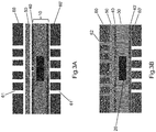
- an electrical power assembly 200 according to a third embodiment of the present invention will be now described.
- the bottom internal thin conductive layer 40' there is no bottom electrically insulating layer between the bottom internal thin conductive layer 40' and the bottom external thick conductive layer 60'.
- the bottom external thick conductive layer 60' is positioned directly on the bottom internal thin conductive layer 40'. Therefore, components parts and elements corresponding to those of the first embodiment are designated by identical numeral references, and details description therefore is omitted.
- the base structure of this embodiment is similar to the base structure of the first embodiment, and is not redundantly described below.
- the power assembly 200 comprises a top thick external conductive layer 60 and a bottom thick external conductive layer, 60' positioned at each side of the base structure 10.
- the top and bottom thick external conductive layers have a thickness greater than the thickness of the internal conductive layers of the base structure in order to enhance the current and thermal capabilities of the package structure.
- the thick external conductive layers 60, 60' may have a thickness of about 100 ⁇ m-4mm, preferably about 400 ⁇ m-1mm.
- the material of these layers is metal, preferably copper.
- each external thick electrically conductive layer 60, 60' comprises plural pre-drilled through holes 61, 61' which are formed by mechanical process or other appropriate technique. These predrilled through holes are served as conductive vias holes for connecting the external thick conductive layers 60, 60' to the contact pads of the internal conductive layers 40, 40' as will be explained in more details below.
- the power assembly 200 further comprises a top internal insulating layer 50 disposed between the top external thick conductive layer 60 and the top internal thin electrically conductive layer 40 of the base structure 10.
- the internal insulating layer 50 is made of resin or any appropriate insulating material with high thermal conductivity.
- the electrical power assembly 200 comprises a set of top holes 62 extending from the top internal layer 40, through the top insulating layer 50 and the top thick external layer 60.
- each top hole 62 has a bottom 66 and an open end 67.
- the bottom of the hole is formed by a portion of the contact pads of the top internal conductive layer 40.
- the open end 67 is formed at the surface 65 of the top external thick electrically conductive layer 60.
- Each top hole 62 is formed in part by a hole formed in the top internal insulating layer 50 and in part by the pre-drilled through hole 61 formed in the top external thick conductive layers 60.
- the electrical power assembly 200 comprises also a set of bottom holes 62' extending from the bottom internal electrical layer 40' to the bottom thick external electrically layer 60'.
- the bottom holes 62' are formed directly by the pre-drilled holes 61' formed in the bottom external thick conductive layer 60'.
- top and bottom holes 62, 62' are then filled by a conductive material in order to form the top conductive vias 64 and the bottom conductive vias 64'.
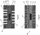
- the holes 62, 62' may be fully filled with the conductive material from the bottom of the holes until the surface of the external thick conductive layer as shown in figure 3D . This step of filling allows making a mechanical adherence between the internal conductive layer 40, 40' and the respective thick conductive layers 60, 60'.
- the contact pads of the top internal conductive layer 40 are connected to the top external thick conductive layer 60 by the top vias 64 arranged in the top internal insulating layer 50 and in the top external thick conductive layer 60.
- the contacts pads of the bottom internal conductive layer 40' are directly connected to the bottom external thick conductive layer 60' by the bottom vias 64'.
- top vias 64 and the bottom vias 64' provide a thermal path for heat dissipation of the power device.
- Figure 4 is a schematic cross-sectional view illustrating a power assembly 500 according to a fourth embodiment of the present invention.
- the power assembly of this embodiment comprises plural power devices, for instance four power devices 521, 521, 523, 524, two diodes and two IGBT.
- the configuration of the power devices is similar to the embodiment shown in figure 2 .
- the electrical contacts of the top side of each power device are connected to the top external thick conductive layer 560 through the top vias 512 formed in the electrically insulating core 530, the internal thin conductive layer 540, the external top vias 564 formed in the top internal insulating layer 550 and in the top external conductive layer 560.
- the electrical contacts of the bottom side of each power device are connected to the bottom external thick conductive layer 560' through the bottom vias 512' formed in the electrically insulating core 530, the bottom internal thin conductive layer 540', the external bottom vias 564' formed by the pre-drilled holes of the bottom external conductive layer 560'.
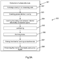
- FIG. 5A and 5B a manufacturing method 300 of an electrical power assembly as shown in figures 1A-1G according to an embodiment of the present invention will now be described.
- the method of forming the electrical assembly as shown in figures 2 , 3 and 4 is similar and is not redundantly described.
- the figure 5A illustrates an example of the formation 301 of the multilayer base structure 10.
- At step 302 at least one cavity is formed in an insulating core.
- the cavity may be obtained for instance by mechanical drilling.
- the shape of the cavity is adapted to the power device.
- a power device 20 is inserted in the cavity.
- the power device may be a diode or a transistor such as a MOSFET, JFET or IGBT and can have the various configurations of electrical contacts. Moreover the number of the power devices can be also varied according to the electronic function requirements.
- Each power device is oriented in the cavity in a manner that the electrical contacts of the power device are facing upwardly and downwardly.
- the insulating core comprising the power device is positioned between two additional insulating layers and two thin internal conductive layers 40, 40', to obtain a stack.
- the stack of insulating layers and the conductive layers 40, 40' are laminated in order to form a solid multilayer structure, in which the insulating layers of the stack are fused together to form an insulating core 30 as shown in figure 1A .
- the power device 20 is embedded inside the insulating core 30.
- the method then comprises a step 306 of forming a set of top holes 11 in the insulating core 30 and in the top internal conductive layer 40 and a set of bottom holes 11' in the insulating core 30 and in the bottom conductive layer 40'.
- the holes 11, 11' are formed by a laser drilling process in order to expose the electrical contacts of the power device.
- the holes are plated with conductive material such as copper by an electroplating process in order to form conductive vias 12, 12'.
- the plating may be performed by electro less or/and electro plating.
- the conductive material is copper.
- the solid multilayer structure is dipped into two plating baths in order to fully fill the holes.
- an etching step is applied on the surface of the top and bottom internal conductive layers 40, 40' in order to form the desired conductive patterns on both side of the base structure. These conductive patterns will be used as contacts pads.
- two thick conductive layers 60, 60' having pre-drilled through holes are provided.
- the thick conductive layers have a thickness of about 400 ⁇ m - 4 mm.
- the external electrical conductive layers comprise pre-drilled through holes which have a diameter of about 500 ⁇ m - 1000 ⁇ m.
- the holes of the thick conductive layers are formed by a mechanical process.
- the base structure 10 is positioned between two additional internal electrically insulating layers 50, 50' and two thick external electrically conductive layers 60, 60' for forming a new stack.
- the bottom external thick conductive layer 60' is positioned directly on the surface of the bottom internal thin conductive layer 40' as show in figure 3A .
- the stack comprising the base structure, the two additional internal electrically insulating layers and the two additional thick conductive layers is laminated in order to form a solid multilayer structure.
- the epoxy resin present in the insulating layers flows and fill the pre-drilled through holes 61, 61' of the thick external conductive layers 60, 60'.
- the pre-drilled through holes 61, 61' may be pre-filled with a paste insulating material during the step 308.
- the material may be epoxy, silicon or other any appropriate material that can be easily cleaned for the plating step.
- each hole 62, 62' has a bottom 66, 66' formed by a portion of a contact pad of the internal conductive layers 40, 40' and an open end 67, 67' at the surface of the external thick conductive layers 60, 60'.
- This removing step can be performed by any appropriate process such as laser, chemical, mechanical, plasma process.
- the holes 62, 62' are filled with conductive material 63 in order to form conductive vias 64, 64' to connect the contact pads of the internal conductive layers 40, 40' to the external thick conductive layers 60, 60'.
- the structure is dipped into two plating bath. The first is electroless plating in order to connect the internal thin conductive layers to the external thick conductive layers. The second bath is used to fully fill the holes with conductive material.
- the surface of the top thick conductive layer and the bottom thick conductive layer are patterned either by etching or milling.
- the conductive patterns may be served as contact pads for the power assembly. Consequently, several power assemblies may be inserted or integrated into another multilayer structure to form a power module.
- the method may comprise further steps wherein the sequence of steps 309 to 313 is repeated at least once.
- the power assembly as shown in figures 1G , 2 , 3D and 4 can be again positioned between two additional insulating layers and thick conductive layers comprising pred-drilled holes.
- the sequence of steps 309 to 313 may be repeated a number of times necessary to obtain a desired total thickness for the external conductive layers on each side of the base structure. This thickness which is also required for increasing the power and thermal transmission may be in a range of between 1 mm and 100 mm.
Landscapes
- Engineering & Computer Science (AREA)
- Microelectronics & Electronic Packaging (AREA)
- Manufacturing & Machinery (AREA)
- Production Of Multi-Layered Print Wiring Board (AREA)
Priority Applications (5)
| Application Number | Priority Date | Filing Date | Title |
|---|---|---|---|
| EP19164827.8A EP3716326A1 (de) | 2019-03-25 | 2019-03-25 | Elektrische leistungsanordnung mit dicken elektrisch leitfähigen schichten |
| JP2021558153A JP7214008B2 (ja) | 2019-03-25 | 2020-01-20 | 厚い導電層を備える電気パワーアセンブリ |
| US17/431,916 US11791254B2 (en) | 2019-03-25 | 2020-01-20 | Electrically power assembly with thick electrically conductive layers |
| PCT/JP2020/002641 WO2020195089A1 (en) | 2019-03-25 | 2020-01-20 | Electrically power assembly with thick electrically conductive layers |
| CN202080020447.9A CN113632223B (zh) | 2019-03-25 | 2020-01-20 | 具有厚导电层的电力组件 |
Applications Claiming Priority (1)
| Application Number | Priority Date | Filing Date | Title |
|---|---|---|---|
| EP19164827.8A EP3716326A1 (de) | 2019-03-25 | 2019-03-25 | Elektrische leistungsanordnung mit dicken elektrisch leitfähigen schichten |
Publications (1)
| Publication Number | Publication Date |
|---|---|
| EP3716326A1 true EP3716326A1 (de) | 2020-09-30 |
Family
ID=65911054
Family Applications (1)
| Application Number | Title | Priority Date | Filing Date |
|---|---|---|---|
| EP19164827.8A Pending EP3716326A1 (de) | 2019-03-25 | 2019-03-25 | Elektrische leistungsanordnung mit dicken elektrisch leitfähigen schichten |
Country Status (5)
| Country | Link |
|---|---|
| US (1) | US11791254B2 (de) |
| EP (1) | EP3716326A1 (de) |
| JP (1) | JP7214008B2 (de) |
| CN (1) | CN113632223B (de) |
| WO (1) | WO2020195089A1 (de) |
Families Citing this family (1)
| Publication number | Priority date | Publication date | Assignee | Title |
|---|---|---|---|---|
| EP4403871B1 (de) * | 2023-01-23 | 2025-09-17 | Mitsubishi Electric R&D Centre Europe B.V. | Mechanische ermüdungsüberwachung für leistungsmodulverpackung |
Citations (4)
| Publication number | Priority date | Publication date | Assignee | Title |
|---|---|---|---|---|
| US20020108776A1 (en) * | 2001-02-13 | 2002-08-15 | Fujitsu Limited | Multilayer printed circuit board and method of making the same |
| EP2854168A2 (de) * | 2013-09-26 | 2015-04-01 | General Electric Company | Eingebettetes Halbleitervorrichtungsgehäuse und Verfahren zur Herstellung davon |
| EP3148300A1 (de) * | 2015-09-24 | 2017-03-29 | AT & S Austria Technologie & Systemtechnik Aktiengesellschaft | Verbindungssystem für elektronische komponenten |
| EP3252812A2 (de) * | 2016-05-31 | 2017-12-06 | Delta Electronics Int'l (Singapore) Pte Ltd | Eingebettete verpackungsstruktur |
Family Cites Families (10)
| Publication number | Priority date | Publication date | Assignee | Title |
|---|---|---|---|---|
| JP3610247B2 (ja) * | 1998-10-30 | 2005-01-12 | 京セラ株式会社 | 配線基板 |
| JP2004140063A (ja) * | 2002-10-16 | 2004-05-13 | O K Print:Kk | 配線基板 |
| KR100631922B1 (ko) * | 2004-02-23 | 2006-10-04 | 삼성전자주식회사 | 개선된 열 확산 성능을 갖는 다층 회로 보오드 및 그에따른 제조방법 |
| JP4361826B2 (ja) * | 2004-04-20 | 2009-11-11 | 新光電気工業株式会社 | 半導体装置 |
| US8692364B2 (en) * | 2009-08-07 | 2014-04-08 | Nec Corporation | Semiconductor device and method for manufacturing the same |
| JP5273095B2 (ja) * | 2010-05-24 | 2013-08-28 | 株式会社デンソー | 半導体装置 |
| JP5381926B2 (ja) * | 2010-07-27 | 2014-01-08 | 株式会社デンソー | 半導体装置 |
| SG10201400396WA (en) * | 2014-03-05 | 2015-10-29 | Delta Electronics Int’L Singapore Pte Ltd | Package structure and stacked package module with the same |
| JP2016058417A (ja) * | 2014-09-05 | 2016-04-21 | 日本特殊陶業株式会社 | 半導体パワーモジュールの製造方法 |
| EP3547359A1 (de) * | 2018-03-30 | 2019-10-02 | Mitsubishi Electric R&D Centre Europe B.V. | Verbesserte vorverpackte leistungszelle |
-
2019
- 2019-03-25 EP EP19164827.8A patent/EP3716326A1/de active Pending
-
2020
- 2020-01-20 JP JP2021558153A patent/JP7214008B2/ja active Active
- 2020-01-20 WO PCT/JP2020/002641 patent/WO2020195089A1/en not_active Ceased
- 2020-01-20 CN CN202080020447.9A patent/CN113632223B/zh active Active
- 2020-01-20 US US17/431,916 patent/US11791254B2/en active Active
Patent Citations (4)
| Publication number | Priority date | Publication date | Assignee | Title |
|---|---|---|---|---|
| US20020108776A1 (en) * | 2001-02-13 | 2002-08-15 | Fujitsu Limited | Multilayer printed circuit board and method of making the same |
| EP2854168A2 (de) * | 2013-09-26 | 2015-04-01 | General Electric Company | Eingebettetes Halbleitervorrichtungsgehäuse und Verfahren zur Herstellung davon |
| EP3148300A1 (de) * | 2015-09-24 | 2017-03-29 | AT & S Austria Technologie & Systemtechnik Aktiengesellschaft | Verbindungssystem für elektronische komponenten |
| EP3252812A2 (de) * | 2016-05-31 | 2017-12-06 | Delta Electronics Int'l (Singapore) Pte Ltd | Eingebettete verpackungsstruktur |
Also Published As
| Publication number | Publication date |
|---|---|
| JP7214008B2 (ja) | 2023-01-27 |
| CN113632223B (zh) | 2024-01-12 |
| US20220148958A1 (en) | 2022-05-12 |
| CN113632223A (zh) | 2021-11-09 |
| JP2022515931A (ja) | 2022-02-22 |
| WO2020195089A1 (en) | 2020-10-01 |
| US11791254B2 (en) | 2023-10-17 |
Similar Documents
| Publication | Publication Date | Title |
|---|---|---|
| EP3996473B1 (de) | Komponententräger mit elektronischen komponenten und thermisch leitfähigen blöcken auf beiden seiten | |
| US20160133558A1 (en) | Power Module | |
| EP3584833B1 (de) | Leistungsmodul mit verbesserter ausrichtung | |
| US10770444B2 (en) | Electronics package having a multi-thickness conductor layer and method of manufacturing thereof | |
| WO2018084957A1 (en) | Stacked electronics package and method of manufacturing thereof | |
| KR101986855B1 (ko) | 발광 부품용 회로와 그 제조 방법 | |
| CN112713120A (zh) | 功率电子组件及其产生方法 | |
| WO2019187400A1 (en) | Pre-packed power cell, power module and method for manufacturing pre-packed power cell | |
| WO2024061467A1 (en) | Prepackage module for embedding into a multilayer printed circuit board | |
| TWI657546B (zh) | 設有電隔離件及基底板之線路板、其半導體組體及其製法 | |
| CN107134441B (zh) | 具有可焊接的电接触部的芯片嵌入封装体 | |
| US20180040562A1 (en) | Elektronisches modul und verfahren zu seiner herstellung | |
| US11791254B2 (en) | Electrically power assembly with thick electrically conductive layers | |
| US20240128197A1 (en) | Assemblies with embedded semiconductor device modules and related methods | |
| Böttcher et al. | Concepts for realizing High-Voltage Power Modules by Embedding of SiC Semiconductors | |
| KR20230136459A (ko) | 전력 반도체 모듈 및 전력 반도체 모듈의 제조 방법 | |
| KR20230042373A (ko) | 전자 회로 모듈 | |
| US20250105129A1 (en) | Laminate carrier with embedded electronic component electrically coupled with protruding pin | |
| CN118234111A (zh) | 一种功率线路板封装和散热器一体化产品及其制备方法 | |
| CN118786527A (zh) | 具有嵌入式半导体器件模块的组件及相关方法 | |
| KR20250094625A (ko) | 매립된 반도체 디바이스 모듈을 갖는 어셈블리 및 관련 방법 | |
| CN119053022A (zh) | 芯片埋入式印刷电路板结构及其制备方法 | |
| JP2020167232A (ja) | モジュールおよびその製造方法 |
Legal Events
| Date | Code | Title | Description |
|---|---|---|---|
| PUAI | Public reference made under article 153(3) epc to a published international application that has entered the european phase |
Free format text: ORIGINAL CODE: 0009012 |
|
| STAA | Information on the status of an ep patent application or granted ep patent |
Free format text: STATUS: THE APPLICATION HAS BEEN PUBLISHED |
|
| AK | Designated contracting states |
Kind code of ref document: A1 Designated state(s): AL AT BE BG CH CY CZ DE DK EE ES FI FR GB GR HR HU IE IS IT LI LT LU LV MC MK MT NL NO PL PT RO RS SE SI SK SM TR |
|
| AX | Request for extension of the european patent |
Extension state: BA ME |
|
| STAA | Information on the status of an ep patent application or granted ep patent |
Free format text: STATUS: REQUEST FOR EXAMINATION WAS MADE |
|
| 17P | Request for examination filed |
Effective date: 20201218 |
|
| RBV | Designated contracting states (corrected) |
Designated state(s): AL AT BE BG CH CY CZ DE DK EE ES FI FR GB GR HR HU IE IS IT LI LT LU LV MC MK MT NL NO PL PT RO RS SE SI SK SM TR |
|
| STAA | Information on the status of an ep patent application or granted ep patent |
Free format text: STATUS: EXAMINATION IS IN PROGRESS |
|
| 17Q | First examination report despatched |
Effective date: 20220425 |