EP3254155B1 - Dispositif d'alignement à l'état de polarisation (psa) - Google Patents
Dispositif d'alignement à l'état de polarisation (psa) Download PDFInfo
- Publication number
- EP3254155B1 EP3254155B1 EP16758475.4A EP16758475A EP3254155B1 EP 3254155 B1 EP3254155 B1 EP 3254155B1 EP 16758475 A EP16758475 A EP 16758475A EP 3254155 B1 EP3254155 B1 EP 3254155B1
- Authority
- EP
- European Patent Office
- Prior art keywords
- light
- polarization
- output
- coupled
- pbs
- Prior art date
- Legal status (The legal status is an assumption and is not a legal conclusion. Google has not performed a legal analysis and makes no representation as to the accuracy of the status listed.)
- Active
Links
Images

Classifications
-
- H—ELECTRICITY
- H04—ELECTRIC COMMUNICATION TECHNIQUE
- H04B—TRANSMISSION
- H04B10/00—Transmission systems employing electromagnetic waves other than radio-waves, e.g. infrared, visible or ultraviolet light, or employing corpuscular radiation, e.g. quantum communication
- H04B10/60—Receivers
- H04B10/61—Coherent receivers
- H04B10/614—Coherent receivers comprising one or more polarization beam splitters, e.g. polarization multiplexed [PolMux] X-PSK coherent receivers, polarization diversity heterodyne coherent receivers
-
- H—ELECTRICITY
- H04—ELECTRIC COMMUNICATION TECHNIQUE
- H04B—TRANSMISSION
- H04B10/00—Transmission systems employing electromagnetic waves other than radio-waves, e.g. infrared, visible or ultraviolet light, or employing corpuscular radiation, e.g. quantum communication
- H04B10/25—Arrangements specific to fibre transmission
- H04B10/2507—Arrangements specific to fibre transmission for the reduction or elimination of distortion or dispersion
- H04B10/2572—Arrangements specific to fibre transmission for the reduction or elimination of distortion or dispersion due to forms of polarisation-dependent distortion other than PMD
-
- H—ELECTRICITY
- H04—ELECTRIC COMMUNICATION TECHNIQUE
- H04B—TRANSMISSION
- H04B10/00—Transmission systems employing electromagnetic waves other than radio-waves, e.g. infrared, visible or ultraviolet light, or employing corpuscular radiation, e.g. quantum communication
- H04B10/50—Transmitters
- H04B10/501—Structural aspects
- H04B10/503—Laser transmitters
- H04B10/505—Laser transmitters using external modulation
- H04B10/5053—Laser transmitters using external modulation using a parallel, i.e. shunt, combination of modulators
-
- H—ELECTRICITY
- H04—ELECTRIC COMMUNICATION TECHNIQUE
- H04B—TRANSMISSION
- H04B10/00—Transmission systems employing electromagnetic waves other than radio-waves, e.g. infrared, visible or ultraviolet light, or employing corpuscular radiation, e.g. quantum communication
- H04B10/50—Transmitters
- H04B10/516—Details of coding or modulation
- H04B10/532—Polarisation modulation
-
- H—ELECTRICITY
- H04—ELECTRIC COMMUNICATION TECHNIQUE
- H04B—TRANSMISSION
- H04B10/00—Transmission systems employing electromagnetic waves other than radio-waves, e.g. infrared, visible or ultraviolet light, or employing corpuscular radiation, e.g. quantum communication
- H04B10/60—Receivers
- H04B10/61—Coherent receivers
- H04B10/615—Arrangements affecting the optical part of the receiver
- H04B10/6151—Arrangements affecting the optical part of the receiver comprising a polarization controller at the receiver's input stage
-
- G—PHYSICS
- G02—OPTICS
- G02B—OPTICAL ELEMENTS, SYSTEMS OR APPARATUS
- G02B6/00—Light guides; Structural details of arrangements comprising light guides and other optical elements, e.g. couplings
- G02B6/24—Coupling light guides
- G02B6/26—Optical coupling means
- G02B6/27—Optical coupling means with polarisation selective and adjusting means
- G02B6/2706—Optical coupling means with polarisation selective and adjusting means as bulk elements, i.e. free space arrangements external to a light guide, e.g. polarising beam splitters
- G02B6/2713—Optical coupling means with polarisation selective and adjusting means as bulk elements, i.e. free space arrangements external to a light guide, e.g. polarising beam splitters cascade of polarisation selective or adjusting operations
- G02B6/272—Optical coupling means with polarisation selective and adjusting means as bulk elements, i.e. free space arrangements external to a light guide, e.g. polarising beam splitters cascade of polarisation selective or adjusting operations comprising polarisation means for beam splitting and combining
Definitions
- Optical fibers are widely used for providing communications links. Communications links employing optical fibers provide many advantages compared to communications links employing electrical media. Those advantages include larger bandwidth, higher noise immunity, reduced power dissipation, and reduced crosstalk. The rapid growth of optical communications links and the need for greater capacity has led research and industry to employ more advanced and higher-order modulation schemes. Napasab, V. et al.: “New Polarization-State Control Scheme: Polarization Recombining.” Optics Communications, Elsevier, Amsterdam, NL, vol. 66, no.
- pages 83-87 discloses an automated polarization-state control scheme consisting of a polarization beam splitter, a 90°-linear polarization rotator, an endless phaseshifter and a beam combiner.
- Napasab, V. et al.: “Endless all-fibre linear polarization phase shifter", Journal of Physics E. Scientific Instruments, IOP Publishing, Bristol, GB, vol. 21, no. 10, 1 October 1988, pages 974-977 discloses a technique for continuous phase shifting of a linearly polarised light wave which is based on a simple polarisation rotating scheme.
- an endless all-fibre linear polarisation phase shifter can be constructed.
- This device also operates as a linear polarisation rotator.
- US 2014/376929 A1 discloses an optical receiver comprising a package provided with an input window; a polarization-maintaining optical fiber fixable to the input window; a polarization beam splitter, disposed on the package, for inputting light outputted from the polarization-maintaining optical fiber and outputting first output light and second output light having respective polarization directions different from each other; a beam splitter, disposed on the package, for splitting the first output light; a first light-receiving element, optically coupled to the beam splitter, having two light-receiving parts corresponding to two kinds of the output light split by the beam splitter; and a second light-receiving element, disposed on the package, for receiving the second output light.
- US 2014/286651 A1 discloses an optical receiver for coherent optical communication, including a splitting element that splits a signal light into two optical axes; optical hybrids each of which is coupled with the two split optical axes; a skew adjustment element that is arranged on one of the optical axes, and adjusts a difference between optical path lengths of the two optical axes between the splitting element and the optical hybrids; a carrier; an adhesive that is filled between the skew adjustment element and the carrier; and a void that is located at an end portion of an optical axis direction of the skew adjustment element in a region where the skew adjustment element and the carrier are opposed to each other, the void being not filled up with the adhesive.
- the disclosure includes a system comprising: a polarization state aligner (PSA) comprising: an input port; a first polarization beam splitter (PBS) coupled to the input port; a first phase shifter (PS) coupled to the first PBS; a first polarization rotator (PR) coupled to the first PBS; a first beam splitter (BS) coupled to the first PS and the first PR; a first output port coupled to the first BS; and a second output port coupled to the first BS.
- PSA polarization state aligner
- PBS polarization beam splitter
- PR phase shifter
- PR polarization rotator
- BS beam splitter
- the system further comprises: a receiver coupled to the PSA and comprising: a second PBS; a first 90 degree (°) hybrid mixer coupled to the second PBS and the first output port; first photodiodes (PDs) coupled to the first 90° hybrid mixer; first transimpedance amplifiers (TIAs) coupled to the first PDs; and a digital signal processor (DSP) coupled to the first TIAs;
- the system further comprises: a second PR coupled to the second PBS; a second 90° hybrid mixer coupled to the second PR and the BS; second PDs coupled to the second 90° hybrid mixer; and second TIAs coupled to the second PDs and the DSP;
- the system further comprises: a modulator system coupled to the PSA and comprising: an in-phase (I) modulator coupled to the first output port; a quadrature phase (Q) modulator coupled to the second output port; a second PS coupled to the Q modulator; and a beam combiner (BC) coupled to the I modulator and the second PS
- the disclosure includes a system comprising: a polarization state aligner (PSA) configured to: receive an input light from an optical component at an input polarization; split the input light into a first light and a second light, wherein the first light comprises an output polarization corresponding to an optoelectronic circuit, and wherein the second light comprises a first polarization; rotate the first polarization to the output polarization; combine the first light and the second light; and provide to the optoelectronic circuit a first output light associated with the first light and a second output light associated with the second light; wherein the first output light and the second output light comprise the output polarization;
- the input polarization is any arbitrary polarization
- the output polarization is a transverse electric (TE) polarization
- the first polarization is a transverse magnetic (TM) polarization
- the PSA comprises: a polarization beam splitter (PBS) configured to: receive the input light; and split the input light into the
- PBS
- the disclosure includes a method comprising: receiving an input light from an optical component at an input polarization; splitting the input light into a first light and a second light, wherein the first light comprises an output polarization corresponding to an optoelectronic circuit, and wherein the second light comprises a first polarization; rotating the first polarization to the output polarization; shifting a phase of the first light, the second light, or both so that a phase delay between the first light and the second light equalizes a first power of a first output light to a second power of a second output light; combining the first light and the second light; and providing to the optoelectronic circuit the first output light and the second output light, wherein the first output light is associated with the first light and the second output light is associated with the second light; wherein the first output light and the second output light comprise the output polarization.
- the method further comprises: providing to a coherent receiver the first output light as a first local oscillator (LO) optical signal; and providing to the coherent receiver the second output light as a second LO optical signal; the method further comprises: providing to a modulator system the first output light as a first continuous wave (CW) light; and providing to the modulator system the second output light as a second CW light.
- LO local oscillator
- CW continuous wave
- High-speed optical transceivers are key components in optical communications systems.
- Systems that combine advanced modulation formats such as higher-order quadrature amplitude modulation (QAM) with coherent detection have shown high performance and high capacity.
- coherent detection refers to the detection of both amplitude information and phase information in order to recover a signal.
- Such advanced modulation formats are implemented in both a transmitter and a receiver.
- a modulator such as an in-phase and quadrature phase (IQ) modulator modulates data onto a continuous wave (CW) light to produce a modulated optical signal.
- CW continuous wave
- modulation is polarization dependent, so a CW laser and the modulator need to have matching polarizations.
- an integrated coherent receiver (ICR) receives the modulated optical signal and a local oscillator (LO) optical signal, wherein the LO optical signal beats with the modulated optical signal in order for the ICR to recover phase information.
- LO optical signal local oscillator
- Such recovery is polarization dependent, so the LO optical signal and the ICR need to have matching polarizations.
- both the transmitter and the receiver need polarization alignment between their respective components.
- the PSAs receive light beams or signals from fibers or other optical components, adjust the polarizations of the light beams or signals to desired polarizations of optoelectronic circuits, and pass the light beams or signals to the optoelectronic circuits.
- the optoelectronic circuits comprise IQ modulators, ICRs, or other components.
- the PSAs address the polarization dependence of those components. Because the PSAs adjust the polarizations of the lights to desired polarizations, the PSAs allow for use of SSMFs and other fibers, which are not polarization maintaining, instead of PMFs.
- the PSAs reduce cost, particularly when longer fibers are needed to couple components.
- multiple laser sources may be in an end of row (EoR) switch, and modulators corresponding to the laser sources may be relatively far away in a top of rack (ToR) switch and coupled to the laser sources via SSMFs.
- multiple laser sources may be in a base band unit (BBU), and modulators corresponding to the laser sources may be relatively far away in a remote radio unit (RRU) and coupled to the laser sources via SSMFs.
- RRU remote radio unit
- a LO optical signal source may be relatively far away and coupled to a coherent receiver via a SSMF.
- relatively far away may mean at least a few meters (m) and up to tens of kilometers (km).
- the PSAs reduce costs for short-haul applications in particular, the PSAs may also be used in metro applications.
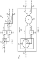
- FIG. 1 is a schematic diagram of a PSA 100 according to an embodiment of the disclosure.
- the PSA 100 comprises an input port 110, a polarization beam splitter (PBS) 120, a phase shifter (PS) 130, a polarization rotator (PR) 140, a beam splitter (BS) 150, an output port 160, and an output port 170.
- the lines connecting those components represent light beams or signals.
- the light beams or signals are labeled as variants of the letter "E," which indicates an optical field in root square watts (W 1/2 ).
- the light beams or signals are labeled with their polarizations at various points.
- the polarizations include transverse electric (TE) and transverse magnetic (TM).
- the light travels through air in a free-space optics application or through an optical waveguide medium comprising silicon (Si), silicon dioxide (SiO 2 ), indium phosphide (InP), or other suitable material in a waveguide application.
- the PS 130 is shown in a top branch of the PSA 100, the PS 130 may instead be in a bottom branch of the PSA 100 or be in both the top branch and the bottom branch of the PSA 100.
- an input light E in enters the PSA 100 through the input port 110.
- E in may enter from an SSMF and therefore have any arbitrary polarization.
- E in passes from the input port 110 to the PBS 120.
- the PBS 120 splits E in into a first light E 1 with a TE polarization and a second light E 2 with a TM polarization.
- the PBS 120 then passes E 1 to the PS 130 and E 2 to the PR 140.
- the PS 130 performs a phase shift of E 1 as described below and passes E 1 to the BS 150. After the phase shift of E 1 , the difference in phase between E 1 and E 2 is referred to as a phase delay.
- the PR 140 rotates E 2 90 degrees (°) so that E 2 has a TE polarization, and the PR 140 passes E 2 to the BS 150.
- the BS 150 receives both E 1 and E 2 , combines E 1 and E 2 , and passes E out,1 to the output port 160 and E out,2 to the output port 170.
- E 1 and E 2 have the same power.
- E 1 and E 2 have the same TE polarization, which may be the desired polarization of a subsequent optoelectronic circuit.
- E out,1 and E out,2 have the same TE polarization and have the same power.
- E 1 is an optical field of a light entering the BS 150 from the top branch of the PSA 100
- E 0 is an amplitude of an optical field of E in
- e is an exponential function
- j is an imaginary number
- ⁇ is an optical carrier frequency in units of hertz (Hz)
- t time in units of second (s)
- ⁇ is an optical phase that may include phase noise and is in units of radians
- ⁇ is a relative angle between a polarization of E in and a TE polarization of the PBS 120 and is in units of degrees (°)
- E 2 is an optical field of the light entering the BS 150 from the bottom branch of the PSA 100
- ⁇
- a processor which is described below, performs the calculations and instructs the PS 130 to perform the phase shift of E 1 based on the calculations.
- the PS 130 may be a heater or phase modulator. If the PS 130 is a heater, then the PS 130 provides a heat based on instructions from the processor. If the PS 130 is a phase modulator, then the PS 130 provides a voltage or current based on the instructions from the processor.
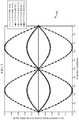
- FIG. 2 is a graph 200 of output as a function of phase delay for various values of a relative angle for the PSA 100 in FIG. 1 .
- the x-axis represents the phase delay ⁇ in x ⁇ radians, where x is between 0 and 2.
- the value 1 indicates that the phase delay ⁇ ⁇ is 1 ⁇ radians.
- the y-axis represents output power relative to input power in arbitrary or constant units.
- the value 0.5 indicates that P out,1 is half of P 0 .
- the relative angle is ⁇ , and its various values are 0°, 45°, and 80°.
- the relative powers of P 1 and P 2 vary with ⁇ ⁇ and have a complementary relationship.
- the time delay ⁇ can be designed to be zero to reduce wavelength dependence. However, fabrication may introduce some variation in ⁇ so that ⁇ is not zero.
- ⁇ is a single value, but the optical carrier frequency ⁇ may vary due to a wavelength drift.
- the wavelength drift may be ⁇ 6.5 nanometers (nm) for an uncooled coarse wavelength-division multiplexing (CWDM) laser, but the wavelength drift is typically relatively slow.
- CWDM coarse wavelength-division multiplexing
- the wavelength drift can be tracked, and the wavelength drift can be compensated for by adjusting the phase delay ⁇ ⁇ .
- FSR free spectral range
- GHz gigahertz
- An FSR of 100 GHz corresponds to a time delay ⁇ of 10 picoseconds (ps), so the length difference, or tolerance, between the top branch of the PSA 100 and the bottom branch of the PSA 100 is about 0.75 millimeters (mm) for a silicon waveguide with a refractive index of about 4. That tolerance is realistic for available fabrication techniques.
- FIG. 3 is a schematic diagram of an integrated PSA 300 according to an embodiment of the disclosure.
- the PSA 300 comprises a substrate 310, an input port 320, a polarization splitter-rotator (PSR) 330, a PS 340, an optical coupler (OC) 350, an output port 360, and an output port 370.
- the PSA 300 is referred to as an integrated PSA because, unlike for the PSA 100, the components of the PSA 300 are integrated into or onto the substrate 310 during fabrication.
- the substrate 310 comprises silicon. Light travels through a silicon-based optical waveguide.
- E in enters the PSA 100 through the input port 320.
- E in may enter from an SSMF and therefore have any arbitrary polarization.
- E in passes from the input port 320 to the PSR 330.
- the PSR 330 splits E in into a first light E 1 with a TE polarization and a second light E 2 with a TM polarization.
- the PSR 330 then passes E 1 to the OC 350.
- the PSR 330 rotates E 2 90° so that E 2 has a TE polarization, and the PSR 330 passes E 2 to the PS 340.
- the PS 340 performs a phase shift of E 2 as described above and passes E 2 to the OC 350.
- the OC 350 receives both E 1 and E 2 , combines E 1 and E 2 , and passes E out,1 to the output port 360 and E out,2 to the output port 370.
- E 1 and E 2 have the same power.
- E 1 and E 2 have the same TE polarization, which may be the desired polarization of a subsequent optoelectronic circuit.
- E out,1 and E out,2 have the same TE polarization and have the same power.
- Equations (1)-(6) apply to E 1 , E 2 , E out,1 , and E out,2 in the PSA 300 as they do to the PSA 100 in FIG. 1 , except the light paths are reversed. For instance, equation (1) applies to E 2 and equation (2) applies to E 1 .
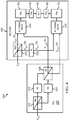
- FIG. 4 is a schematic diagram of a dual-polarization coherent receiver system 400 according to an embodiment of the disclosure.
- the system 400 generally comprises a PSA 405, which is similar to the PSA 100, and a receiver 440.
- the system 400 provides one implementation of the PSA 100.
- the PSA 405 may replace a PBS in other dual-polarization coherent receiver systems.
- the PSA 405 and the receiver 440 may be integrated on a silicon substrate.
- the PSA 405 comprises a PBS 410, a PS 415, a PR 420, and a BS 425 that are similar to the PBS 120, the PS 130, the PR 140, and the BS 150, respectively, in the PSA 100.
- the receiver 440 is a dual-polarization coherent receiver and comprises a PBS 430, a PR 435, a 90° hybrid mixer 445, photodiodes (PDs) 450, transimpedance amplifiers (TIAs) 455, a digital signal processor (DSP) 460, a 90° hybrid mixer 475, PDs 470, and TIAs 465. Though the PDs 450, 470 and the TIAs 455, 465 are shown as single components, they may represent four or any suitable number of PDs or TIAs.
- the PSA 405 receives an LO optical signal E LO from an LO optical signal source, which may be relatively far away from the system 400 in a transmitter. If the LO optical signal source is coupled to the system 400 via an SSMF, then the polarization of the E LO may vary with time. Nonetheless, as described for the PSA 100, the PSA 405 provides E LO,X and E LO,Y , which have the same TE polarization and the same power.
- E LO,X is a LO optical signal for an X polarization component
- E LO,Y is a LO optical signal for a Y polarization component.
- the receiver 440 receives a modulated optical signal E S from a signal source, which likewise may be relatively far away from the system 400 in a transmitter.
- the PBS 430 splits E S into a E S,X , which has a TE polarization, and E S,Y , which has a TM polarization.
- the PR 435 rotates the polarization of E S,Y to a TE polarization.
- the 90° hybrid mixer 445 introduces a 90° phase shift between E S,X and E S,Y , which the PDs 450 detect, the TIAs 455 amplify, and the DSP 460 converts from analog to digital and then processes.
- the 90° hybrid mixer 475 introduces a 90° phase shift between E LO,X and E LO,Y , which the PDs 470 detect, the TIAs 465 amplify, and the DSP 460 converts from analog to digital and then processes.
- SHD Self-homodyne detection
- E S,X E sig , X t s e j ⁇ t s + ⁇ sig t s + ⁇ t s
- E sig,X is a signal waveform
- t s is a time in units of seconds
- ⁇ sig is a phase encoded by data
- ⁇ is phase noise.
- E LO,0 is an optical field amplitude of E LO
- t lo is an LO time in units of seconds.
- I XI 1 2 E sig , X t s E LO , 0 1 ⁇ sin ⁇ ⁇ + ⁇ sin 2 ⁇ cos ⁇ XI
- I XQ 1 2 E sig , X t s E LO , 0 1 ⁇ sin ⁇ ⁇ + ⁇ sin 2 ⁇ sin ⁇ XQ ⁇ ⁇ XI and ⁇ ⁇ XQ , in turn, are expressed as follows:
- ⁇ becomes part of the total extracted phase difference. Except for a data-modulated phase term, other phase contributions vary relatively slowly, so they can be tracked and compensated for by the DSP 460.
- the X polarization components I XI and I XQ are described above, but the same equations apply for the Y polarization components I YI and I YQ .
- the system 400 is a single-wavelength, dual-polarization, coherent optical receiver system.
- the scheme may be extended to multiple-wavelength systems.
- a wavelength-division multiplexing (WDM) multiplexer is placed before the system 400, the WDM multiplexer outputs M wavelengths, and M PSAs are placed after the WDM multiplexer so that each wavelength is associated with a separate PSA.
- WDM wavelength-division multiplexing
- M PSAs are placed after the WDM multiplexer so that each wavelength is associated with a separate PSA.
- two multiplexers are placed after the PSA 405.
- One multiplexer is for an X polarization component
- one multiplexer is for a Y polarization component. The two multiplexers then output M wavelengths.
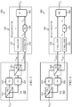
- FIG. 5 is a schematic diagram of an IQ transmitter system 500 according to an embodiment of the disclosure.
- the system 500 generally comprises a PSA 505, which is similar to the PSA 100, and a modulator system 530.
- the system 500 provides an implementation of the PSA 100.
- the PSA 505 and the modulator system 530 may be integrated on a silicon substrate.
- the PSA 505 comprises a PBS 510, a PS 515, a PR 520, and a BS 525 that are similar to the PBS 120, the PS 130, the PR 140, and the BS 150, respectively, in the PSA 100.
- the modulator system 530 comprises an I modulator 535, a Q modulator 540, a PS 545, and a beam combiner (BC) 550.
- the I modulator 535 and the Q modulator 535 may be Mach-Zehnder modulators (MZMs).
- the PSA 505 receives E CW from a CW source, which may be relatively far away from the system 500. If the CW source is coupled to the system 500 via a SSMF, then the polarization of E CW may vary with time. Nonetheless, as described for the PSAs 100, 405, the PSA 505 provides E CW,I and E CW,Q , which have the same TE polarization and the same power.
- the TE polarization corresponds to the polarization orientation of the I modulator 535 and the Q modulator 540.
- the I modulator 535 modulates E CW,I with data to produce E I , then passes E I to the BC 550.
- the Q modulator 540 modulates E CW,Q with data to produce E Q , then passes E Q to the PS 545.
- the PS 545 adds a phase change to E Q to create a 90° phase difference between E I and E Q .
- the BC 550 combines E I and E Q into a single light E out , then outputs E out .
- FIG. 6 is a schematic diagram of a dual-polarization transmitter system 600 according to an embodiment of the disclosure.
- the system 600 generally comprises a PSA 605, which is similar to the PSA 100, and a modulator system 630.
- the system 600 provides an implementation of the PSA 100.
- the PSA 605 and the modulator system 630 may be integrated on a silicon substrate.
- the PSA 605 comprises a PBS 610, a PS 615, a PR 620, and a BS 625 that are similar to the PBS 120, the PS 130, the PR 140, and the BS 150, respectively, in the PSA 100.
- the modulator system 630 comprises an X component (X) modulator 635, a Y component (Y) modulator 640, a PR 645, and a polarization beam combiner (PBC) 650.
- the X modulator 635 and the Y modulator 640 may be MZMs, electro-absorption (EA) modulators, or IQ modulators and may provide non-return-to-zero modulation, quadrature phase shift keying, 16-level quadrature amplitude modulator (16-QAM), or another suitable modulation format.
- EA electro-absorption
- IQ modulators may provide non-return-to-zero modulation, quadrature phase shift keying, 16-level quadrature amplitude modulator (16-QAM), or another suitable modulation format.
- the PSA 605 receives E CW from a CW source, which may be relatively far away from the system 600. If the CW source is coupled to the system 600 via an SSMF, then the polarization of E CW may vary with time. Nonetheless, as described for the PSAs 100, 405, 505, the PSA 605 provides E CW,X and E CW,Y , which have the same TE polarization and the same power.
- the TE polarization corresponds to the polarization orientation of the X modulator 635 and the Y modulator 640.
- the X modulator 635 modulates E CW,X with data to produce E X , then passes E X to the PBC 650.
- the Y modulator 640 modulates E CW,Y with data to produce E Y , then passes E Y to the PR 645.
- the PR 645 rotates E Y so that E Y has a polarization orthogonal to E X .
- the PBC 650 combines E X and E Y into a single light E out , then outputs E out .
- FIG. 7 is a schematic diagram of a PSM4 transmitter system 700 according to an embodiment of the disclosure.
- the system 700 generally comprises a PSA 705, which is similar to the PSA 100, and a modulator system 730.
- the system 700 provides an implementation of the PSA 100.
- the PSA 705 and the modulator system 730 may be integrated on a silicon substrate.
- the PSA comprises a PBS 710, a PS 715, a PR 720, and a BS 725 that are similar to the PBS 120, the PS 130, the PR 140, and the BS 150, respectively, in the PSA 100.
- the modulator system 730 comprises a BS 735, a modulator 740, a modulator 745, a BS 750, a modulator 755, and a modulator 760.
- the modulators 740, 745, 755, 760 may be MZMs.
- the PSA 705 receives E CW from a CW source, which may be relatively far away from the system 700. If the CW source is coupled to the system 700 via an SSMF, then the polarization of E CW may vary with time. Nonetheless, as described for the PSAs 100, 405, 505, 605, the PSA 705 provides E CW,1 and E CW,2 , which have the same TE polarization and the same power.
- the TE polarization corresponds to the polarization orientation of the modulators 740, 745, 755, 760.
- the BS 735 equally splits E CW,1 into E in,1 and E in,2
- the BS 750 equally splits E CW,2 into E in,3 and E in,4 .
- the modulator 740 modulates E in,1 with data to produce E out,1 , then outputs E out,1
- the modulator 745 modulates E in,2 with data to produce E out,2
- the modulator 755 modulates E in,3 with data to produce E out,3
- the modulator 760 modulates E in,4 with data to produce E out,4 , then outputs E out,4 .
- the modulators 740, 745, 755, 760 may output E out,1 , E out,2 , E out,3 , and E out,4 , respectively, to PSM4 fibers.
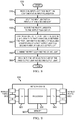
- FIG. 8 is a flowchart illustrating a method 800 of polarization state alignment according to an embodiment of the disclosure.
- the PSAs 100, 300 or the systems 400, 500, 600, 700 may implement the method 800 at any suitable time, for instance upon desiring to provide LO optical signals or optical signals.
- an input light is received from an optical component.
- the input light is at an input polarization.
- the PSA 100 receives E in from an SSMF, and E in comprises an arbitrary polarization.
- the input light is split into a first light and a second light.
- the first light comprises an output polarization corresponding to an optoelectronic circuit
- the second light comprises a first polarization.
- the PBS 120 splits E in into E 1 , which has a TE polarization, and E 2 , which has a TM polarization.
- the first polarization is rotated to the output polarization.
- the PR 140 rotates the polarization of E 2 so that E 2 has a TE polarization.
- a phase of the first light, the second light, or both is shifted so that a phase delay between the first light and the second light equalizes a first power of a first output light to a second power of a second output light.
- the PS 130 shifts the phase of E 1 so that the phase delay between the phase of E 1 and the phase of E 2 is an integer multiple of ⁇ so that P out,1 and P out,2 are equal.
- the first output light and the second output light are provided to the optoelectronic circuit.
- the first output light and the second output light comprise the output polarization.
- the PSA 100 provides E out,1 and E out,2 to a modulator system or a receiver, and E out,1 and E out,2 comprise the TE polarization.
- FIG. 9 is a schematic diagram of a device 900.
- the device 900 is suitable for implementing the disclosed embodiments. For instance, as described above, the device 900 performs calculations to determine an appropriate phase shift and instructs a PS such as the PSs 130, 340, 415, 515, 615, 715 to apply that phase shift.
- the device 900 comprises ingress ports 910 and receiver units (Rx) 920 for receiving data; a processor, logic unit, or central processing unit (CPU) 930 to process the data; transmitter units (Tx) 940 and egress ports 950 for transmitting the data; and a memory 960 for storing the data.
- Rx receiver units
- CPU central processing unit
- the device 900 may also comprise optical-to-electrical (OE) components and electrical-to-optical (EO) components coupled to the ingress ports 910, the receiver units 920, the transmitter units 940, and the egress ports 950 for egress or ingress of optical or electrical signals.
- OE optical-to-electrical
- EO electrical-to-optical
- the processor 930 is implemented by any suitable combination of hardware, middleware, and software.
- the processor 930 may be implemented as one or more CPU chips, cores (e.g., as a multi-core processor), field-programmable gate arrays (FPGAs), application specific integrated circuits (ASICs), and digital signal processors (DSPs).
- the processor 930 is in communication with the ingress ports 910, receiver units 920, transmitter units 940, egress ports 950, and memory 960.
- the memory 960 comprises one or more disks, tape drives, and solid-state drives and may be used as an over-flow data storage device, to store programs when such programs are selected for execution, and to store instructions and data that are read during program execution.
- the memory 960 may be volatile and non-volatile and may be read-only memory (ROM), random-access memory (RAM), ternary content-addressable memory (TCAM), and static random-access memory (SRAM).
- the device 900 includes a light input module receiving an input light from an optical component at an input polarization, a splitter module splitting the input light into a first light and a second light, wherein the first light comprises an output polarization corresponding to an optoelectronic circuit, and wherein the second light comprises a first polarization, a rotation module rotating the first polarization to the output polarization, a phase shift module shifting a phase of the first light, the second light, or both so that a phase delay between the first light and the second light equalizes a first power of a first output light to a second power of a second output light, a combiner module combining the first light and the second light, and a light output module providing to the optoelectronic circuit the first output light and the second output light, wherein the first output light is associated with the first light and the second output light is associated with the second light, wherein the first output light and the second output light comprise the output polarization.
- the device 900 includes a light input module receiving
Landscapes
- Physics & Mathematics (AREA)
- Electromagnetism (AREA)
- Engineering & Computer Science (AREA)
- Computer Networks & Wireless Communication (AREA)
- Signal Processing (AREA)
- Optics & Photonics (AREA)
- Optical Communication System (AREA)
- Optical Modulation, Optical Deflection, Nonlinear Optics, Optical Demodulation, Optical Logic Elements (AREA)
- Optical Integrated Circuits (AREA)
- Instruments For Measurement Of Length By Optical Means (AREA)
- Optical Couplings Of Light Guides (AREA)
Claims (7)
- Système comprenant :
un dispositif d'alignement d'état de polarisation, PSA, (405) comprenant :un port d'entrée (110),un premier séparateur de faisceau de polarisation, PBS, (410) couplé au port d'entrée,un premier déphaseur, PS (415) couplé à la première sortie du premier séparateur PBS (410),un premier rotateur de polarisation, PR, (420) couplé à la seconde sortie du premier séparateur PBS (410),un premier séparateur de faisceau, BS, (425) couplé au premier déphaseur PS (415) et au premier rotateur PR (420),un premier port de sortie couplé au premier séparateur BS (425), et caractérisé par :un second port de sortie couplé au premier séparateur BS (425),un récepteur (440) couplé au dispositif PSA et comprenant :un second séparateur PBS (430),un premier mélangeur hybride 90 ° (445) couplé à la première sortie du second séparateur PBS (430) et au premier port de sortie du premier séparateur BS (425),des premières photodiodes, PD, (450) couplées au premier mélangeur hybride 90 ° (445),des premiers amplificateurs d'adaptation d'impédance, TIA, (455) couplés aux premières diodes PD (450), etun processeur numérique de signal, DSP, (460) couplé aux premiers amplificateurs TIA (455),dans lequel le récepteur (440) comprend en outre :un second rotateur PR (435) couplé à la seconde sortie du second séparateur PBS (430),un second mélangeur hybride 90 ° (475) couplé au second rotateur PR (435) et au second port de sortie du premier séparateur BS (425),des secondes diodes PD (470) couplées au second mélangeur hybride 90 ° (475), etdes seconds amplificateurs TIA (465) couplés aux secondes diodes PD (470) et au processeur DSP (460). - Système selon la revendication 1, comprenant en outre un milieu formant guide d'onde couplant le premier séparateur PBS (410) au port d'entrée, le premier déphaseur PS (415) au premier séparateur PBS (410), le premier rotateur PR (420) au premier séparateur PBS (410) le premier séparateur BS (425) au premier déphaseur PS (415) et au premier rotateur PR (420), le premier port de sortie au premier séparateur BS (425) et le second port de sortie au premier séparateur BS (425).
- Système selon la revendication 1, dans lequel :
le dispositif PSA est configuré pour :recevoir la lumière d'entrée émise par un composant optique au niveau d'une polarisation d'entrée,séparer la lumière d'entrée en une première lumière et une seconde lumière, la première lumière comprenant une polarisation de sortie correspondant à un circuit optoélectronique, et la seconde lumière comprenant une première polarisation,faire tourner la première polarisation pour obtenir la polarisation de sortie, combiner la première lumière et la seconde lumière, etdélivrer au circuit optoélectronique une première lumière de sortie associée à la première lumière et une seconde lumière de sortie associée à la seconde lumière,dans lequel la première lumière de sortie et la seconde lumière de sortie comprennent la polarisation de sortie. - Système selon la revendication 3, dans lequel la polarisation d'entrée est une quelconque polarisation arbitraire, la polarisation de sortie est une polarisation électrique transverse, TE et la première polarisation est une polarisation magnétique transverse, TM.
- Système selon l'une quelconque des revendications 3 à 4, dans lequel :
le premier séparateur PBS (410) est configuré pour :recevoir la lumière d'entrée, etséparer la lumière d'entrée en la première lumière et la seconde lumière,le premier rotateur PR (420) est couplé au premier séparateur PBS (410) et configuré pour faire tourner la première polarisation pour obtenir la polarisation de sortie, etle premier déphaseur PS (415) est couplé au premier séparateur PBS (410) et configuré pour décaler une première phase de la première lumière en une seconde phase de sorte que le retard de phase entre la première lumière et la seconde lumière soit un multiple entier de π. - Système selon l'une quelconque des revendications 3 à 4, dans lequel le dispositif PSA comprend :
un séparateur - rotateur de polarisation (PSR) (330) configuré pour :recevoir la lumière d'entrée,séparer la lumière d'entrée en la première lumière et la seconde lumière, etfaire tourner la première polarisation pour obtenir la polarisation de sortie, etle séparateur PS (340), couplé au séparateur PSR (330) et configuré pour décaler une première phase de la seconde lumière en une seconde phase de sorte que le retard de phase entre la première lumière et la seconde lumière soit un multiple entier de π. - Procédé comprenant :la réception d'une lumière d'entrée émise par un composant optique avec une polarisation d'entrée,la séparation par polarisation de la lumière d'entrée en une première lumière et en une seconde lumière, la première lumière comprenant une polarisation de sortie qui convient à un récepteur cohérent et la seconde lumière comprenant une première polarisation,la rotation de la première polarisation pour obtenir la polarisation de sortie,le décalage de phase de la première lumière, de la seconde lumière ou des deux de sorte que le retard de phase entre la première lumière et la seconde lumière égalise la première puissance d'une première lumière de sortie à la seconde puissance de lumière de sortie,la combinaison de la première lumière et de la seconde lumière et leur séparation en une première lumière de sortie et une seconde lumière de sortie, etla délivrance au récepteur cohérent de la première lumière de sortie et de la seconde lumière de sortie,dans lequel la première lumière de sortie et la seconde lumière de sortie comprennent la polarisation de sortie,caractérisé en ce que le procédé comprend en outre :la délivrance au récepteur cohérent de la première lumière de sortie sous forme d'un premier signal optique d'oscillateur local, LO, etla délivrance au récepteur cohérent de la seconde lumière de sortie sous forme d'un second signal optique d'oscillateur LO.
Priority Applications (1)
| Application Number | Priority Date | Filing Date | Title |
|---|---|---|---|
| EP20211976.4A EP3812831A1 (fr) | 2015-03-02 | 2016-03-02 | Dispositif d'alignement à l'état de polarisation (psa) |
Applications Claiming Priority (3)
| Application Number | Priority Date | Filing Date | Title |
|---|---|---|---|
| US201562127057P | 2015-03-02 | 2015-03-02 | |
| US15/057,379 US9819420B2 (en) | 2015-03-02 | 2016-03-01 | Polarization state aligner (PSA) |
| PCT/CN2016/075335 WO2016138860A1 (fr) | 2015-03-02 | 2016-03-02 | Dispositif d'alignement à l'état de polarisation (psa) |
Related Child Applications (1)
| Application Number | Title | Priority Date | Filing Date |
|---|---|---|---|
| EP20211976.4A Division EP3812831A1 (fr) | 2015-03-02 | 2016-03-02 | Dispositif d'alignement à l'état de polarisation (psa) |
Publications (3)
| Publication Number | Publication Date |
|---|---|
| EP3254155A1 EP3254155A1 (fr) | 2017-12-13 |
| EP3254155A4 EP3254155A4 (fr) | 2018-05-02 |
| EP3254155B1 true EP3254155B1 (fr) | 2020-12-30 |
Family
ID=56848357
Family Applications (2)
| Application Number | Title | Priority Date | Filing Date |
|---|---|---|---|
| EP20211976.4A Pending EP3812831A1 (fr) | 2015-03-02 | 2016-03-02 | Dispositif d'alignement à l'état de polarisation (psa) |
| EP16758475.4A Active EP3254155B1 (fr) | 2015-03-02 | 2016-03-02 | Dispositif d'alignement à l'état de polarisation (psa) |
Family Applications Before (1)
| Application Number | Title | Priority Date | Filing Date |
|---|---|---|---|
| EP20211976.4A Pending EP3812831A1 (fr) | 2015-03-02 | 2016-03-02 | Dispositif d'alignement à l'état de polarisation (psa) |
Country Status (6)
| Country | Link |
|---|---|
| US (1) | US9819420B2 (fr) |
| EP (2) | EP3812831A1 (fr) |
| JP (2) | JP6837440B2 (fr) |
| KR (1) | KR101985926B1 (fr) |
| CN (1) | CN107407828A (fr) |
| WO (1) | WO2016138860A1 (fr) |
Families Citing this family (31)
| Publication number | Priority date | Publication date | Assignee | Title |
|---|---|---|---|---|
| US9647426B1 (en) * | 2013-06-28 | 2017-05-09 | Aurrion, Inc. | Polarization insensitive colorless optical devices |
| WO2016162904A1 (fr) * | 2015-04-10 | 2016-10-13 | National Institute Of Information And Communications Technology | Récepteur pour détection auto-homodyne insensible à la polarisation pour des systèmes de multiplexage à répartition dans l'espace |
| JP2016208276A (ja) * | 2015-04-22 | 2016-12-08 | 富士通株式会社 | プローブ発生装置、光伝送装置及びプローブ発生方法 |
| US10491299B2 (en) * | 2016-03-15 | 2019-11-26 | Oe Solutions America, Inc. | Electronic dispersion compensation methods and implementations using RLC filter synthesis |
| US10171171B2 (en) * | 2016-07-07 | 2019-01-01 | Luxtera, Inc. | Method and system for selectable parallel optical fiber and wavelength division multiplexed operation |
| KR102733630B1 (ko) * | 2016-09-28 | 2024-11-26 | 한국전자통신연구원 | 편광분석형 듀얼 lc 파장필터 모듈 |
| US10551640B2 (en) | 2016-11-21 | 2020-02-04 | Futurewei Technologies, Inc. | Wavelength division multiplexed polarization independent reflective modulators |
| US10222676B2 (en) * | 2017-01-27 | 2019-03-05 | Futurewei Technologies, Inc. | Polarization insensitive integrated optical modulator |
| US10330959B2 (en) | 2017-05-22 | 2019-06-25 | Futurewei Technologies, Inc. | Polarization insensitive micro ring modulator |
| US10243684B2 (en) | 2017-05-23 | 2019-03-26 | Futurewei Technologies, Inc. | Wavelength-division multiplexed polarization-insensitive transmissive modulator |
| JP2018205338A (ja) * | 2017-05-30 | 2018-12-27 | 日本電信電話株式会社 | 偏波無依存化した励起光再生成装置および光中継増幅器 |
| US10928588B2 (en) * | 2017-10-13 | 2021-02-23 | Skorpios Technologies, Inc. | Transceiver module for optical communication |
| US10833767B2 (en) * | 2018-01-24 | 2020-11-10 | Indian Institute Of Technology Bombay | Self-homodyne carrier multiplexed transmission system and method for coherent optical links |
| US10651947B2 (en) * | 2018-02-20 | 2020-05-12 | Futurewei Technologies, Inc. | Coherent detection with remotely delivered local oscillators |
| CN108449132B (zh) * | 2018-03-18 | 2021-01-26 | 中山市威晟光通科技有限公司 | 一种高精度可调光滤波器波长调谐量的测量方法 |
| US10666016B2 (en) * | 2018-05-09 | 2020-05-26 | Elenion Technologies, Llc | Tunable lasers |
| CN108871593A (zh) * | 2018-06-20 | 2018-11-23 | 北京邮电大学 | 一种相干探测系统的高精度自动平衡的方法 |
| US11405125B2 (en) * | 2018-07-12 | 2022-08-02 | Ayar Labs, Inc. | TORminator system and associated methods |
| WO2020103164A1 (fr) * | 2018-11-24 | 2020-05-28 | 华为技术有限公司 | Dispositif de traitement de polarisation, émetteur-récepteur optique, et procédé de traitement de polarisation optique |
| CN109450551B (zh) * | 2018-11-30 | 2020-10-02 | 北京邮电大学 | 一种多倍频程移相方法和装置 |
| CN112054851B (zh) * | 2019-06-05 | 2022-03-29 | 华为技术有限公司 | 相干光接收装置、相干光处理方法和系统 |
| WO2020254080A1 (fr) * | 2019-06-21 | 2020-12-24 | Orange | Detection coherente avec oscillateur local optimise |
| CN113132020B (zh) * | 2019-12-31 | 2023-07-28 | 华为技术有限公司 | 相干光接收装置和采用相干光接收装置的光系统 |
| KR102514006B1 (ko) * | 2020-09-08 | 2023-03-24 | 한국표준과학연구원 | 편광 유지 광섬유를 이용한 전자파 측정 장치 |
| CN114696917B (zh) | 2020-12-30 | 2024-04-09 | 华为技术有限公司 | 相干光接收机、光通信设备及系统 |
| US11641248B2 (en) | 2021-03-01 | 2023-05-02 | Google Llc | System, apparatus, and architecture for migrating an optical communication network |
| US11689292B2 (en) * | 2021-03-01 | 2023-06-27 | Google Llc | Polarization-folding coherent optical technology for short reach optical communication |
| CN115529086A (zh) * | 2021-06-25 | 2022-12-27 | 华为技术有限公司 | 一种相干接收装置,相干接收的方法以及相干通信系统 |
| US11588549B1 (en) * | 2021-08-09 | 2023-02-21 | Mellanox Technologies, Ltd. | Systems, devices, and methods for polarization recovery |
| DE112023001181T5 (de) * | 2022-03-02 | 2024-12-24 | Voyant Photonics, Inc. | Integrierte Polarisationssteuerungssysteme |
| KR102914846B1 (ko) * | 2022-11-21 | 2026-01-20 | 한국전자통신연구원 | 편광 생성 및 분배를 위한 장치 |
Citations (1)
| Publication number | Priority date | Publication date | Assignee | Title |
|---|---|---|---|---|
| WO2014020669A1 (fr) * | 2012-07-30 | 2014-02-06 | 富士通オプティカルコンポーネンツ株式会社 | Circuit de réception de lumière |
Family Cites Families (27)
| Publication number | Priority date | Publication date | Assignee | Title |
|---|---|---|---|---|
| DE3377595D1 (en) * | 1983-12-01 | 1988-09-08 | Ibm Deutschland | Interferometric device with a mach-zehnder interferometer |
| JPH01222216A (ja) * | 1988-03-02 | 1989-09-05 | Toshiba Corp | 導波路型偏波面制御装置 |
| JPH0243520A (ja) * | 1988-08-03 | 1990-02-14 | Toshiba Corp | 光集積回路 |
| JPH05313109A (ja) * | 1992-05-11 | 1993-11-26 | Nippon Telegr & Teleph Corp <Ntt> | 導波路型偏波制御器 |
| JP3284507B2 (ja) * | 1993-06-28 | 2002-05-20 | 富士通株式会社 | 光通信システム用の光送信装置及び光増幅装置 |
| US7031561B2 (en) * | 2001-06-22 | 2006-04-18 | Massachusetts Institute Of Technology | Monolithic integration of micro-optics circuits and RF circuits |
| US20040208646A1 (en) * | 2002-01-18 | 2004-10-21 | Seemant Choudhary | System and method for multi-level phase modulated communication |
| US6853758B2 (en) | 2002-07-12 | 2005-02-08 | Optimer Photonics, Inc. | Scheme for controlling polarization in waveguides |
| EP2653899B1 (fr) * | 2007-01-10 | 2016-06-22 | Nippon Telegraph And Telephone Corporation | Circuit d'interférence optique de type guide d'ondes |
| US8238759B2 (en) * | 2008-02-14 | 2012-08-07 | Infinera Corporation | High capacity transmitter implemented on a photonic integrated circuit |
| JP2010060656A (ja) * | 2008-09-01 | 2010-03-18 | Fujitsu Ltd | 偏光状態安定化方法及び装置、光信号処理システム |
| US8032025B2 (en) * | 2008-10-22 | 2011-10-04 | Opnext Subsystems, Inc. | Polarization monitoring in polarization division multiplexing in optical communications |
| US8401405B2 (en) * | 2009-05-28 | 2013-03-19 | Freedom Photonics, Llc. | Monolithic widely-tunable coherent receiver |
| JP5319468B2 (ja) | 2009-09-18 | 2013-10-16 | 日本電信電話株式会社 | 光回路 |
| JP2011188132A (ja) * | 2010-03-05 | 2011-09-22 | Sumitomo Electric Ind Ltd | コヒーレント光通信用受信機及びその光軸調整方法 |
| JP5737874B2 (ja) | 2010-07-06 | 2015-06-17 | 日本オクラロ株式会社 | 復調器及び光送受信機 |
| US8462349B1 (en) * | 2010-07-20 | 2013-06-11 | Science Applications International Corporation | System and method for a self-referencing interferometer |
| US8908189B2 (en) * | 2011-04-15 | 2014-12-09 | Carl Zeiss Meditec, Inc. | Systems and methods for swept-source optical coherence tomography |
| JP5804058B2 (ja) | 2011-07-01 | 2015-11-04 | 日本電気株式会社 | Rz光変調器及びrz光変調方法 |
| JP5700731B2 (ja) | 2011-12-22 | 2015-04-15 | 日本電信電話株式会社 | 光変調器 |
| JP5868341B2 (ja) * | 2012-08-24 | 2016-02-24 | 日本電信電話株式会社 | 光合分波器 |
| JP2014092713A (ja) * | 2012-11-05 | 2014-05-19 | Sumitomo Electric Ind Ltd | 偏波多重光変調器装置、集積光学素子 |
| US8923665B2 (en) * | 2013-03-15 | 2014-12-30 | International Business Machines Corporation | Material structures for front-end of the line integration of optical polarization splitters and rotators |
| JP2014187506A (ja) * | 2013-03-22 | 2014-10-02 | Sumitomo Electric Ind Ltd | 光受信器及びその製造方法 |
| JP6236912B2 (ja) * | 2013-06-24 | 2017-11-29 | 住友電気工業株式会社 | 光受信器及びその光軸調芯方法 |
| CN105612460B (zh) * | 2013-10-09 | 2019-06-21 | Asml荷兰有限公司 | 独立于偏振的干涉仪 |
| CN105308495A (zh) | 2014-05-23 | 2016-02-03 | 华为技术有限公司 | 偏振控制器件和偏振控制的方法 |
-
2016
- 2016-03-01 US US15/057,379 patent/US9819420B2/en not_active Expired - Fee Related
- 2016-03-02 KR KR1020177027994A patent/KR101985926B1/ko active Active
- 2016-03-02 WO PCT/CN2016/075335 patent/WO2016138860A1/fr not_active Ceased
- 2016-03-02 JP JP2017546117A patent/JP6837440B2/ja active Active
- 2016-03-02 EP EP20211976.4A patent/EP3812831A1/fr active Pending
- 2016-03-02 EP EP16758475.4A patent/EP3254155B1/fr active Active
- 2016-03-02 CN CN201680012763.5A patent/CN107407828A/zh active Pending
-
2020
- 2020-07-07 JP JP2020117217A patent/JP2020170197A/ja active Pending
Patent Citations (1)
| Publication number | Priority date | Publication date | Assignee | Title |
|---|---|---|---|---|
| WO2014020669A1 (fr) * | 2012-07-30 | 2014-02-06 | 富士通オプティカルコンポーネンツ株式会社 | Circuit de réception de lumière |
Non-Patent Citations (1)
| Title |
|---|
| NAPASAB V ET AL: "POLARIZATION RECOMBINING: A NEW AUTOMATIC POLARIZATION CONTROL SCHEME FOR HETERODYNE OR HOMODYNE OPTICAL RECEIVERS", JOURNAL OF OPTICAL COMMUNICATIONS, FACHVERLAG SCHIELE & SCHON, BERLIN, DE, vol. 9, no. 9, 1 September 1988 (1988-09-01), pages 102 - 107, XP000000862, ISSN: 0173-4911 * |
Also Published As
| Publication number | Publication date |
|---|---|
| JP6837440B2 (ja) | 2021-03-03 |
| KR20170125390A (ko) | 2017-11-14 |
| JP2018508828A (ja) | 2018-03-29 |
| EP3254155A4 (fr) | 2018-05-02 |
| US20160261352A1 (en) | 2016-09-08 |
| EP3812831A1 (fr) | 2021-04-28 |
| CN107407828A (zh) | 2017-11-28 |
| EP3254155A1 (fr) | 2017-12-13 |
| US9819420B2 (en) | 2017-11-14 |
| JP2020170197A (ja) | 2020-10-15 |
| WO2016138860A1 (fr) | 2016-09-09 |
| WO2016138860A8 (fr) | 2016-12-15 |
| KR101985926B1 (ko) | 2019-09-03 |
Similar Documents
| Publication | Publication Date | Title |
|---|---|---|
| EP3254155B1 (fr) | Dispositif d'alignement à l'état de polarisation (psa) | |
| US7529490B2 (en) | Optical receiver and optical reception method compatible with differential quadrature phase shift keying | |
| US10944482B2 (en) | Coherent optical receiver | |
| EP2446310B1 (fr) | Récepteur optique cohérent | |
| US10164405B2 (en) | Wavelength locker integrated with a silicon photonics system | |
| US8548333B2 (en) | Transceiver photonic integrated circuit | |
| US20230090061A1 (en) | Systems, devices, and methods for dual polarization recovery | |
| US20160127070A1 (en) | Integrated two-channel spectral combiner and wavelength locker in silicon photonics | |
| US12323233B2 (en) | System, apparatus, and architecture for migrating an optical communication network | |
| Dong et al. | Monolithic silicon photonic circuits enable 112-Gb/s PDMQPSK transmission over 2560-km SSMF | |
| Noé et al. | LiNbO3-based endless optical polarization control | |
| US20250062832A1 (en) | Electronic demultiplexing for dual-polarization (dp) intensity-modulated direct detection (imdd) optical communication systems | |
| Sakamaki et al. | One-chip integrated polarisation-multiplexed DQPSK demodulator using silica-based planar lightwave circuit technology | |
| Kim et al. | Hybrid Integrated Photonic Circuits for High Bandwidth Coherent Receivers in Optical Communication Networks | |
| US20120301158A1 (en) | Optical Receiver | |
| Hibino | Integrated photonic devices for advanced modulation formats |
Legal Events
| Date | Code | Title | Description |
|---|---|---|---|
| STAA | Information on the status of an ep patent application or granted ep patent |
Free format text: STATUS: THE INTERNATIONAL PUBLICATION HAS BEEN MADE |
|
| PUAI | Public reference made under article 153(3) epc to a published international application that has entered the european phase |
Free format text: ORIGINAL CODE: 0009012 |
|
| STAA | Information on the status of an ep patent application or granted ep patent |
Free format text: STATUS: REQUEST FOR EXAMINATION WAS MADE |
|
| 17P | Request for examination filed |
Effective date: 20170905 |
|
| AK | Designated contracting states |
Kind code of ref document: A1 Designated state(s): AL AT BE BG CH CY CZ DE DK EE ES FI FR GB GR HR HU IE IS IT LI LT LU LV MC MK MT NL NO PL PT RO RS SE SI SK SM TR |
|
| AX | Request for extension of the european patent |
Extension state: BA ME |
|
| RIC1 | Information provided on ipc code assigned before grant |
Ipc: G02B 6/27 20060101ALI20171214BHEP Ipc: G02F 1/01 20060101AFI20171214BHEP Ipc: G01J 4/00 20060101ALI20171214BHEP |
|
| RIC1 | Information provided on ipc code assigned before grant |
Ipc: G02F 1/01 20060101AFI20180321BHEP Ipc: G02B 6/27 20060101ALI20180321BHEP Ipc: G01J 4/00 20060101ALI20180321BHEP |
|
| A4 | Supplementary search report drawn up and despatched |
Effective date: 20180403 |
|
| DAV | Request for validation of the european patent (deleted) | ||
| DAX | Request for extension of the european patent (deleted) | ||
| STAA | Information on the status of an ep patent application or granted ep patent |
Free format text: STATUS: EXAMINATION IS IN PROGRESS |
|
| 17Q | First examination report despatched |
Effective date: 20190722 |
|
| REG | Reference to a national code |
Ref country code: DE Ref legal event code: R079 Ref document number: 602016050623 Country of ref document: DE Free format text: PREVIOUS MAIN CLASS: G02F0001010000 Ipc: H04B0010250700 |
|
| RIC1 | Information provided on ipc code assigned before grant |
Ipc: H04B 10/50 20130101ALI20200429BHEP Ipc: H04B 10/61 20130101ALI20200429BHEP Ipc: H04B 10/2507 20130101AFI20200429BHEP Ipc: G02B 6/27 20060101ALI20200429BHEP |
|
| GRAP | Despatch of communication of intention to grant a patent |
Free format text: ORIGINAL CODE: EPIDOSNIGR1 |
|
| STAA | Information on the status of an ep patent application or granted ep patent |
Free format text: STATUS: GRANT OF PATENT IS INTENDED |
|
| INTG | Intention to grant announced |
Effective date: 20200716 |
|
| GRAS | Grant fee paid |
Free format text: ORIGINAL CODE: EPIDOSNIGR3 |
|
| GRAA | (expected) grant |
Free format text: ORIGINAL CODE: 0009210 |
|
| STAA | Information on the status of an ep patent application or granted ep patent |
Free format text: STATUS: THE PATENT HAS BEEN GRANTED |
|
| AK | Designated contracting states |
Kind code of ref document: B1 Designated state(s): AL AT BE BG CH CY CZ DE DK EE ES FI FR GB GR HR HU IE IS IT LI LT LU LV MC MK MT NL NO PL PT RO RS SE SI SK SM TR |
|
| REG | Reference to a national code |
Ref country code: GB Ref legal event code: FG4D |
|
| REG | Reference to a national code |
Ref country code: AT Ref legal event code: REF Ref document number: 1350978 Country of ref document: AT Kind code of ref document: T Effective date: 20210115 |
|
| REG | Reference to a national code |
Ref country code: DE Ref legal event code: R096 Ref document number: 602016050623 Country of ref document: DE |
|
| REG | Reference to a national code |
Ref country code: IE Ref legal event code: FG4D |
|
| PG25 | Lapsed in a contracting state [announced via postgrant information from national office to epo] |
Ref country code: NO Free format text: LAPSE BECAUSE OF FAILURE TO SUBMIT A TRANSLATION OF THE DESCRIPTION OR TO PAY THE FEE WITHIN THE PRESCRIBED TIME-LIMIT Effective date: 20210330 Ref country code: RS Free format text: LAPSE BECAUSE OF FAILURE TO SUBMIT A TRANSLATION OF THE DESCRIPTION OR TO PAY THE FEE WITHIN THE PRESCRIBED TIME-LIMIT Effective date: 20201230 Ref country code: GR Free format text: LAPSE BECAUSE OF FAILURE TO SUBMIT A TRANSLATION OF THE DESCRIPTION OR TO PAY THE FEE WITHIN THE PRESCRIBED TIME-LIMIT Effective date: 20210331 Ref country code: FI Free format text: LAPSE BECAUSE OF FAILURE TO SUBMIT A TRANSLATION OF THE DESCRIPTION OR TO PAY THE FEE WITHIN THE PRESCRIBED TIME-LIMIT Effective date: 20201230 |
|
| REG | Reference to a national code |
Ref country code: AT Ref legal event code: MK05 Ref document number: 1350978 Country of ref document: AT Kind code of ref document: T Effective date: 20201230 |
|
| PG25 | Lapsed in a contracting state [announced via postgrant information from national office to epo] |
Ref country code: SE Free format text: LAPSE BECAUSE OF FAILURE TO SUBMIT A TRANSLATION OF THE DESCRIPTION OR TO PAY THE FEE WITHIN THE PRESCRIBED TIME-LIMIT Effective date: 20201230 Ref country code: BG Free format text: LAPSE BECAUSE OF FAILURE TO SUBMIT A TRANSLATION OF THE DESCRIPTION OR TO PAY THE FEE WITHIN THE PRESCRIBED TIME-LIMIT Effective date: 20210330 Ref country code: LV Free format text: LAPSE BECAUSE OF FAILURE TO SUBMIT A TRANSLATION OF THE DESCRIPTION OR TO PAY THE FEE WITHIN THE PRESCRIBED TIME-LIMIT Effective date: 20201230 |
|
| REG | Reference to a national code |
Ref country code: NL Ref legal event code: MP Effective date: 20201230 |
|
| PG25 | Lapsed in a contracting state [announced via postgrant information from national office to epo] |
Ref country code: HR Free format text: LAPSE BECAUSE OF FAILURE TO SUBMIT A TRANSLATION OF THE DESCRIPTION OR TO PAY THE FEE WITHIN THE PRESCRIBED TIME-LIMIT Effective date: 20201230 |
|
| REG | Reference to a national code |
Ref country code: LT Ref legal event code: MG9D |
|
| PG25 | Lapsed in a contracting state [announced via postgrant information from national office to epo] |
Ref country code: PT Free format text: LAPSE BECAUSE OF FAILURE TO SUBMIT A TRANSLATION OF THE DESCRIPTION OR TO PAY THE FEE WITHIN THE PRESCRIBED TIME-LIMIT Effective date: 20210430 Ref country code: RO Free format text: LAPSE BECAUSE OF FAILURE TO SUBMIT A TRANSLATION OF THE DESCRIPTION OR TO PAY THE FEE WITHIN THE PRESCRIBED TIME-LIMIT Effective date: 20201230 Ref country code: SK Free format text: LAPSE BECAUSE OF FAILURE TO SUBMIT A TRANSLATION OF THE DESCRIPTION OR TO PAY THE FEE WITHIN THE PRESCRIBED TIME-LIMIT Effective date: 20201230 Ref country code: LT Free format text: LAPSE BECAUSE OF FAILURE TO SUBMIT A TRANSLATION OF THE DESCRIPTION OR TO PAY THE FEE WITHIN THE PRESCRIBED TIME-LIMIT Effective date: 20201230 Ref country code: CZ Free format text: LAPSE BECAUSE OF FAILURE TO SUBMIT A TRANSLATION OF THE DESCRIPTION OR TO PAY THE FEE WITHIN THE PRESCRIBED TIME-LIMIT Effective date: 20201230 Ref country code: EE Free format text: LAPSE BECAUSE OF FAILURE TO SUBMIT A TRANSLATION OF THE DESCRIPTION OR TO PAY THE FEE WITHIN THE PRESCRIBED TIME-LIMIT Effective date: 20201230 |
|
| PG25 | Lapsed in a contracting state [announced via postgrant information from national office to epo] |
Ref country code: AT Free format text: LAPSE BECAUSE OF FAILURE TO SUBMIT A TRANSLATION OF THE DESCRIPTION OR TO PAY THE FEE WITHIN THE PRESCRIBED TIME-LIMIT Effective date: 20201230 Ref country code: PL Free format text: LAPSE BECAUSE OF FAILURE TO SUBMIT A TRANSLATION OF THE DESCRIPTION OR TO PAY THE FEE WITHIN THE PRESCRIBED TIME-LIMIT Effective date: 20201230 |
|
| PG25 | Lapsed in a contracting state [announced via postgrant information from national office to epo] |
Ref country code: IS Free format text: LAPSE BECAUSE OF FAILURE TO SUBMIT A TRANSLATION OF THE DESCRIPTION OR TO PAY THE FEE WITHIN THE PRESCRIBED TIME-LIMIT Effective date: 20210430 |
|
| REG | Reference to a national code |
Ref country code: DE Ref legal event code: R097 Ref document number: 602016050623 Country of ref document: DE |
|
| PG25 | Lapsed in a contracting state [announced via postgrant information from national office to epo] |
Ref country code: AL Free format text: LAPSE BECAUSE OF FAILURE TO SUBMIT A TRANSLATION OF THE DESCRIPTION OR TO PAY THE FEE WITHIN THE PRESCRIBED TIME-LIMIT Effective date: 20201230 Ref country code: IT Free format text: LAPSE BECAUSE OF FAILURE TO SUBMIT A TRANSLATION OF THE DESCRIPTION OR TO PAY THE FEE WITHIN THE PRESCRIBED TIME-LIMIT Effective date: 20201230 Ref country code: MC Free format text: LAPSE BECAUSE OF FAILURE TO SUBMIT A TRANSLATION OF THE DESCRIPTION OR TO PAY THE FEE WITHIN THE PRESCRIBED TIME-LIMIT Effective date: 20201230 |
|
| REG | Reference to a national code |
Ref country code: CH Ref legal event code: PL |
|
| PLBE | No opposition filed within time limit |
Free format text: ORIGINAL CODE: 0009261 |
|
| STAA | Information on the status of an ep patent application or granted ep patent |
Free format text: STATUS: NO OPPOSITION FILED WITHIN TIME LIMIT |
|
| PG25 | Lapsed in a contracting state [announced via postgrant information from national office to epo] |
Ref country code: DK Free format text: LAPSE BECAUSE OF FAILURE TO SUBMIT A TRANSLATION OF THE DESCRIPTION OR TO PAY THE FEE WITHIN THE PRESCRIBED TIME-LIMIT Effective date: 20201230 |
|
| 26N | No opposition filed |
Effective date: 20211001 |
|
| REG | Reference to a national code |
Ref country code: BE Ref legal event code: MM Effective date: 20210331 |
|
| PG25 | Lapsed in a contracting state [announced via postgrant information from national office to epo] |
Ref country code: ES Free format text: LAPSE BECAUSE OF FAILURE TO SUBMIT A TRANSLATION OF THE DESCRIPTION OR TO PAY THE FEE WITHIN THE PRESCRIBED TIME-LIMIT Effective date: 20201230 Ref country code: IE Free format text: LAPSE BECAUSE OF NON-PAYMENT OF DUE FEES Effective date: 20210302 Ref country code: CH Free format text: LAPSE BECAUSE OF NON-PAYMENT OF DUE FEES Effective date: 20210331 Ref country code: LI Free format text: LAPSE BECAUSE OF NON-PAYMENT OF DUE FEES Effective date: 20210331 Ref country code: LU Free format text: LAPSE BECAUSE OF NON-PAYMENT OF DUE FEES Effective date: 20210302 |
|
| PG25 | Lapsed in a contracting state [announced via postgrant information from national office to epo] |
Ref country code: SI Free format text: LAPSE BECAUSE OF FAILURE TO SUBMIT A TRANSLATION OF THE DESCRIPTION OR TO PAY THE FEE WITHIN THE PRESCRIBED TIME-LIMIT Effective date: 20201230 |
|
| PG25 | Lapsed in a contracting state [announced via postgrant information from national office to epo] |
Ref country code: IS Free format text: LAPSE BECAUSE OF FAILURE TO SUBMIT A TRANSLATION OF THE DESCRIPTION OR TO PAY THE FEE WITHIN THE PRESCRIBED TIME-LIMIT Effective date: 20210430 |
|
| PG25 | Lapsed in a contracting state [announced via postgrant information from national office to epo] |
Ref country code: BE Free format text: LAPSE BECAUSE OF NON-PAYMENT OF DUE FEES Effective date: 20210331 |
|
| P01 | Opt-out of the competence of the unified patent court (upc) registered |
Effective date: 20230524 |
|
| PG25 | Lapsed in a contracting state [announced via postgrant information from national office to epo] |
Ref country code: NL Free format text: LAPSE BECAUSE OF NON-PAYMENT OF DUE FEES Effective date: 20201230 Ref country code: CY Free format text: LAPSE BECAUSE OF FAILURE TO SUBMIT A TRANSLATION OF THE DESCRIPTION OR TO PAY THE FEE WITHIN THE PRESCRIBED TIME-LIMIT Effective date: 20201230 |
|
| PG25 | Lapsed in a contracting state [announced via postgrant information from national office to epo] |
Ref country code: SM Free format text: LAPSE BECAUSE OF FAILURE TO SUBMIT A TRANSLATION OF THE DESCRIPTION OR TO PAY THE FEE WITHIN THE PRESCRIBED TIME-LIMIT Effective date: 20201230 Ref country code: HU Free format text: LAPSE BECAUSE OF FAILURE TO SUBMIT A TRANSLATION OF THE DESCRIPTION OR TO PAY THE FEE WITHIN THE PRESCRIBED TIME-LIMIT; INVALID AB INITIO Effective date: 20160302 |
|
| PG25 | Lapsed in a contracting state [announced via postgrant information from national office to epo] |
Ref country code: MK Free format text: LAPSE BECAUSE OF FAILURE TO SUBMIT A TRANSLATION OF THE DESCRIPTION OR TO PAY THE FEE WITHIN THE PRESCRIBED TIME-LIMIT Effective date: 20201230 |
|
| PG25 | Lapsed in a contracting state [announced via postgrant information from national office to epo] |
Ref country code: MT Free format text: LAPSE BECAUSE OF FAILURE TO SUBMIT A TRANSLATION OF THE DESCRIPTION OR TO PAY THE FEE WITHIN THE PRESCRIBED TIME-LIMIT Effective date: 20201230 |
|
| PGFP | Annual fee paid to national office [announced via postgrant information from national office to epo] |
Ref country code: DE Payment date: 20250204 Year of fee payment: 10 |
|
| PGFP | Annual fee paid to national office [announced via postgrant information from national office to epo] |
Ref country code: FR Payment date: 20250210 Year of fee payment: 10 |
|
| PGFP | Annual fee paid to national office [announced via postgrant information from national office to epo] |
Ref country code: GB Payment date: 20250130 Year of fee payment: 10 |
|
| PG25 | Lapsed in a contracting state [announced via postgrant information from national office to epo] |
Ref country code: TR Free format text: LAPSE BECAUSE OF FAILURE TO SUBMIT A TRANSLATION OF THE DESCRIPTION OR TO PAY THE FEE WITHIN THE PRESCRIBED TIME-LIMIT Effective date: 20201230 |