EP3255742A1 - Emballage à montage en surface pour lasers à émission en surface de cavité verticale à grande vitesse - Google Patents
Emballage à montage en surface pour lasers à émission en surface de cavité verticale à grande vitesse Download PDFInfo
- Publication number
- EP3255742A1 EP3255742A1 EP17179558.6A EP17179558A EP3255742A1 EP 3255742 A1 EP3255742 A1 EP 3255742A1 EP 17179558 A EP17179558 A EP 17179558A EP 3255742 A1 EP3255742 A1 EP 3255742A1
- Authority
- EP
- European Patent Office
- Prior art keywords
- array
- submount
- module
- vcsel
- optical
- Prior art date
- Legal status (The legal status is an assumption and is not a legal conclusion. Google has not performed a legal analysis and makes no representation as to the accuracy of the status listed.)
- Granted
Links
Images


















Classifications
-
- H—ELECTRICITY
- H01—ELECTRIC ELEMENTS
- H01S—DEVICES USING THE PROCESS OF LIGHT AMPLIFICATION BY STIMULATED EMISSION OF RADIATION [LASER] TO AMPLIFY OR GENERATE LIGHT; DEVICES USING STIMULATED EMISSION OF ELECTROMAGNETIC RADIATION IN WAVE RANGES OTHER THAN OPTICAL
- H01S5/00—Semiconductor lasers
- H01S5/40—Arrangement of two or more semiconductor lasers, not provided for in groups H01S5/02 - H01S5/30
- H01S5/42—Arrays of surface emitting lasers
- H01S5/423—Arrays of surface emitting lasers having a vertical cavity
-
- F—MECHANICAL ENGINEERING; LIGHTING; HEATING; WEAPONS; BLASTING
- F21—LIGHTING
- F21V—FUNCTIONAL FEATURES OR DETAILS OF LIGHTING DEVICES OR SYSTEMS THEREOF; STRUCTURAL COMBINATIONS OF LIGHTING DEVICES WITH OTHER ARTICLES, NOT OTHERWISE PROVIDED FOR
- F21V29/00—Protecting lighting devices from thermal damage; Cooling or heating arrangements specially adapted for lighting devices or systems
- F21V29/50—Cooling arrangements
- F21V29/70—Cooling arrangements characterised by passive heat-dissipating elements, e.g. heat-sinks
- F21V29/74—Cooling arrangements characterised by passive heat-dissipating elements, e.g. heat-sinks with fins or blades
-
- F—MECHANICAL ENGINEERING; LIGHTING; HEATING; WEAPONS; BLASTING
- F21—LIGHTING
- F21L—LIGHTING DEVICES OR SYSTEMS THEREOF, BEING PORTABLE OR SPECIALLY ADAPTED FOR TRANSPORTATION
- F21L4/00—Electric lighting devices with self-contained electric batteries or cells
- F21L4/02—Electric lighting devices with self-contained electric batteries or cells characterised by the provision of two or more light sources
-
- F—MECHANICAL ENGINEERING; LIGHTING; HEATING; WEAPONS; BLASTING
- F21—LIGHTING
- F21V—FUNCTIONAL FEATURES OR DETAILS OF LIGHTING DEVICES OR SYSTEMS THEREOF; STRUCTURAL COMBINATIONS OF LIGHTING DEVICES WITH OTHER ARTICLES, NOT OTHERWISE PROVIDED FOR
- F21V29/00—Protecting lighting devices from thermal damage; Cooling or heating arrangements specially adapted for lighting devices or systems
- F21V29/50—Cooling arrangements
- F21V29/56—Cooling arrangements using liquid coolants
-
- F—MECHANICAL ENGINEERING; LIGHTING; HEATING; WEAPONS; BLASTING
- F21—LIGHTING
- F21V—FUNCTIONAL FEATURES OR DETAILS OF LIGHTING DEVICES OR SYSTEMS THEREOF; STRUCTURAL COMBINATIONS OF LIGHTING DEVICES WITH OTHER ARTICLES, NOT OTHERWISE PROVIDED FOR
- F21V29/00—Protecting lighting devices from thermal damage; Cooling or heating arrangements specially adapted for lighting devices or systems
- F21V29/50—Cooling arrangements
- F21V29/60—Cooling arrangements characterised by the use of a forced flow of gas, e.g. air
- F21V29/65—Cooling arrangements characterised by the use of a forced flow of gas, e.g. air the gas flowing in a closed circuit
-
- F—MECHANICAL ENGINEERING; LIGHTING; HEATING; WEAPONS; BLASTING
- F21—LIGHTING
- F21V—FUNCTIONAL FEATURES OR DETAILS OF LIGHTING DEVICES OR SYSTEMS THEREOF; STRUCTURAL COMBINATIONS OF LIGHTING DEVICES WITH OTHER ARTICLES, NOT OTHERWISE PROVIDED FOR
- F21V29/00—Protecting lighting devices from thermal damage; Cooling or heating arrangements specially adapted for lighting devices or systems
- F21V29/50—Cooling arrangements
- F21V29/60—Cooling arrangements characterised by the use of a forced flow of gas, e.g. air
- F21V29/67—Cooling arrangements characterised by the use of a forced flow of gas, e.g. air characterised by the arrangement of fans
-
- F—MECHANICAL ENGINEERING; LIGHTING; HEATING; WEAPONS; BLASTING
- F21—LIGHTING
- F21V—FUNCTIONAL FEATURES OR DETAILS OF LIGHTING DEVICES OR SYSTEMS THEREOF; STRUCTURAL COMBINATIONS OF LIGHTING DEVICES WITH OTHER ARTICLES, NOT OTHERWISE PROVIDED FOR
- F21V29/00—Protecting lighting devices from thermal damage; Cooling or heating arrangements specially adapted for lighting devices or systems
- F21V29/50—Cooling arrangements
- F21V29/70—Cooling arrangements characterised by passive heat-dissipating elements, e.g. heat-sinks
-
- H—ELECTRICITY
- H01—ELECTRIC ELEMENTS
- H01S—DEVICES USING THE PROCESS OF LIGHT AMPLIFICATION BY STIMULATED EMISSION OF RADIATION [LASER] TO AMPLIFY OR GENERATE LIGHT; DEVICES USING STIMULATED EMISSION OF ELECTROMAGNETIC RADIATION IN WAVE RANGES OTHER THAN OPTICAL
- H01S5/00—Semiconductor lasers
- H01S5/02—Structural details or components not essential to laser action
- H01S5/022—Mountings; Housings
- H01S5/0233—Mounting configuration of laser chips
- H01S5/02345—Wire-bonding
-
- H—ELECTRICITY
- H01—ELECTRIC ELEMENTS
- H01S—DEVICES USING THE PROCESS OF LIGHT AMPLIFICATION BY STIMULATED EMISSION OF RADIATION [LASER] TO AMPLIFY OR GENERATE LIGHT; DEVICES USING STIMULATED EMISSION OF ELECTROMAGNETIC RADIATION IN WAVE RANGES OTHER THAN OPTICAL
- H01S5/00—Semiconductor lasers
- H01S5/40—Arrangement of two or more semiconductor lasers, not provided for in groups H01S5/02 - H01S5/30
- H01S5/4018—Lasers electrically in series
-
- H—ELECTRICITY
- H01—ELECTRIC ELEMENTS
- H01S—DEVICES USING THE PROCESS OF LIGHT AMPLIFICATION BY STIMULATED EMISSION OF RADIATION [LASER] TO AMPLIFY OR GENERATE LIGHT; DEVICES USING STIMULATED EMISSION OF ELECTROMAGNETIC RADIATION IN WAVE RANGES OTHER THAN OPTICAL
- H01S5/00—Semiconductor lasers
- H01S5/005—Optical components external to the laser cavity, specially adapted therefor, e.g. for homogenisation or merging of the beams or for manipulating laser pulses, e.g. pulse shaping
-
- H—ELECTRICITY
- H01—ELECTRIC ELEMENTS
- H01S—DEVICES USING THE PROCESS OF LIGHT AMPLIFICATION BY STIMULATED EMISSION OF RADIATION [LASER] TO AMPLIFY OR GENERATE LIGHT; DEVICES USING STIMULATED EMISSION OF ELECTROMAGNETIC RADIATION IN WAVE RANGES OTHER THAN OPTICAL
- H01S5/00—Semiconductor lasers
- H01S5/02—Structural details or components not essential to laser action
- H01S5/022—Mountings; Housings
- H01S5/023—Mount members, e.g. sub-mount members
- H01S5/02325—Mechanically integrated components on mount members or optical micro-benches
-
- H—ELECTRICITY
- H01—ELECTRIC ELEMENTS
- H01S—DEVICES USING THE PROCESS OF LIGHT AMPLIFICATION BY STIMULATED EMISSION OF RADIATION [LASER] TO AMPLIFY OR GENERATE LIGHT; DEVICES USING STIMULATED EMISSION OF ELECTROMAGNETIC RADIATION IN WAVE RANGES OTHER THAN OPTICAL
- H01S5/00—Semiconductor lasers
- H01S5/02—Structural details or components not essential to laser action
- H01S5/022—Mountings; Housings
- H01S5/0235—Method for mounting laser chips
- H01S5/02355—Fixing laser chips on mounts
- H01S5/0237—Fixing laser chips on mounts by soldering
-
- H—ELECTRICITY
- H01—ELECTRIC ELEMENTS
- H01S—DEVICES USING THE PROCESS OF LIGHT AMPLIFICATION BY STIMULATED EMISSION OF RADIATION [LASER] TO AMPLIFY OR GENERATE LIGHT; DEVICES USING STIMULATED EMISSION OF ELECTROMAGNETIC RADIATION IN WAVE RANGES OTHER THAN OPTICAL
- H01S5/00—Semiconductor lasers
- H01S5/02—Structural details or components not essential to laser action
- H01S5/024—Arrangements for thermal management
- H01S5/02469—Passive cooling, e.g. where heat is removed by the housing as a whole or by a heat pipe without any active cooling element like a TEC
-
- H—ELECTRICITY
- H01—ELECTRIC ELEMENTS
- H01S—DEVICES USING THE PROCESS OF LIGHT AMPLIFICATION BY STIMULATED EMISSION OF RADIATION [LASER] TO AMPLIFY OR GENERATE LIGHT; DEVICES USING STIMULATED EMISSION OF ELECTROMAGNETIC RADIATION IN WAVE RANGES OTHER THAN OPTICAL
- H01S5/00—Semiconductor lasers
- H01S5/02—Structural details or components not essential to laser action
- H01S5/024—Arrangements for thermal management
- H01S5/02476—Heat spreaders, i.e. improving heat flow between laser chip and heat dissipating elements
-
- H—ELECTRICITY
- H01—ELECTRIC ELEMENTS
- H01S—DEVICES USING THE PROCESS OF LIGHT AMPLIFICATION BY STIMULATED EMISSION OF RADIATION [LASER] TO AMPLIFY OR GENERATE LIGHT; DEVICES USING STIMULATED EMISSION OF ELECTROMAGNETIC RADIATION IN WAVE RANGES OTHER THAN OPTICAL
- H01S5/00—Semiconductor lasers
- H01S5/10—Construction or shape of the optical resonator, e.g. extended or external cavity, coupled cavities, bent-guide, varying width, thickness or composition of the active region
- H01S5/14—External cavity lasers
- H01S5/141—External cavity lasers using a wavelength selective device, e.g. a grating or etalon
-
- H—ELECTRICITY
- H01—ELECTRIC ELEMENTS
- H01S—DEVICES USING THE PROCESS OF LIGHT AMPLIFICATION BY STIMULATED EMISSION OF RADIATION [LASER] TO AMPLIFY OR GENERATE LIGHT; DEVICES USING STIMULATED EMISSION OF ELECTROMAGNETIC RADIATION IN WAVE RANGES OTHER THAN OPTICAL
- H01S5/00—Semiconductor lasers
- H01S5/10—Construction or shape of the optical resonator, e.g. extended or external cavity, coupled cavities, bent-guide, varying width, thickness or composition of the active region
- H01S5/18—Surface-emitting [SE] lasers, e.g. having both horizontal and vertical cavities
- H01S5/183—Surface-emitting [SE] lasers, e.g. having both horizontal and vertical cavities having only vertical cavities, e.g. vertical cavity surface-emitting lasers [VCSEL]
- H01S5/18305—Surface-emitting [SE] lasers, e.g. having both horizontal and vertical cavities having only vertical cavities, e.g. vertical cavity surface-emitting lasers [VCSEL] with emission through the substrate, i.e. bottom emission
-
- H—ELECTRICITY
- H01—ELECTRIC ELEMENTS
- H01S—DEVICES USING THE PROCESS OF LIGHT AMPLIFICATION BY STIMULATED EMISSION OF RADIATION [LASER] TO AMPLIFY OR GENERATE LIGHT; DEVICES USING STIMULATED EMISSION OF ELECTROMAGNETIC RADIATION IN WAVE RANGES OTHER THAN OPTICAL
- H01S5/00—Semiconductor lasers
- H01S5/10—Construction or shape of the optical resonator, e.g. extended or external cavity, coupled cavities, bent-guide, varying width, thickness or composition of the active region
- H01S5/18—Surface-emitting [SE] lasers, e.g. having both horizontal and vertical cavities
- H01S5/183—Surface-emitting [SE] lasers, e.g. having both horizontal and vertical cavities having only vertical cavities, e.g. vertical cavity surface-emitting lasers [VCSEL]
- H01S5/18308—Surface-emitting [SE] lasers, e.g. having both horizontal and vertical cavities having only vertical cavities, e.g. vertical cavity surface-emitting lasers [VCSEL] having a special structure for lateral current or light confinement
-
- H—ELECTRICITY
- H10—SEMICONDUCTOR DEVICES; ELECTRIC SOLID-STATE DEVICES NOT OTHERWISE PROVIDED FOR
- H10W—GENERIC PACKAGES, INTERCONNECTIONS, CONNECTORS OR OTHER CONSTRUCTIONAL DETAILS OF DEVICES COVERED BY CLASS H10
- H10W90/00—Package configurations
- H10W90/701—Package configurations characterised by the relative positions of pads or connectors relative to package parts
- H10W90/751—Package configurations characterised by the relative positions of pads or connectors relative to package parts of bond wires
- H10W90/753—Package configurations characterised by the relative positions of pads or connectors relative to package parts of bond wires between laterally-adjacent chips
Definitions
- an optical illuminator module includes a Vertical Cavity Surface Emitting Laser (VCSEL) having a large area terminal and a second terminal.
- the optical illuminator module includes a submount including a first and second bonding pad that are electrically isolated from each other and positioned on a first surface.
- the large area terminal of the VCSEL is bonded to the first bonding pad such that the VCSEL is in thermal contact with the submount.
- the second terminal is electrically connected to the second bonding pad.
- the first and second bonding pads are electrically connected to a corresponding first and second bonding pad located on a second surface of the submount, which is opposite to the first surface of the submount.
- the optical illuminator module can be configured to perform at least one of motion recognition, gesture recognition, and three-dimensional sensing.
- an illuminator includes a plurality of VCSELs forming a monolithic two-dimensional array of VCSELs where light emits through a plurality of emission windows in a direction perpendicular to a first surface an array.
- the VCSELs include a first electrical contact layer positioned on the first surface of the array of VCSELs.
- a transparent carrier substrate is positioned on the first electrical contact layer.
- a second electrical contact is positioned on the second surface of the array of VCSELs, which is opposite to the first surface of the array of VCSELs.
- a trench is located on the second surface of the array of VCSELs. The trench electrically isolates the array of VCSELs from an electrical contact region located on the second surface.
- the VCSEL arrays disclosed in this invention may be surface mounted directly to a heat sink or a heat sink region optionally included in the PCB, for rapid heat dissipation during high-power operation. Furthermore, optical elements are provided for shaping the optical output beam or emission from the VCSEL-optical output may be modified for individual VCSEL elements or for the entire array.
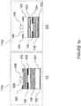
- Figure 1 b(ii) uses the bottom emitting VCSEL structure which is similar to the device described in Figure 1a(ii) except for the following modifications.
- the top reflector 103 is made partially reflecting and a third reflector 100 is fabricated on the top surface of the substrate.
- the combination of reflectors 100 and 103 result in increased reflectivity, when they are in a designed phase relationship, resulting in the desired VCSEL laser operation.
- the output 109 is transmitted by the third reflector 100 and is in the same upward direction.
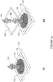
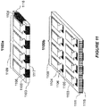
- First electrode of each VCSEL (located underside of the substrate 201 in this example) is connected together to a common first terminal of the array.
- Second electrode of each VCSEL is connected together (top surface of the array 209) to a common second terminal of the array.
- the substrate of the array is the bonding surface and the surface of the array is the emitting surface in this example as well.
- the common substrate also the common first terminal of the array in this example, is bonded to a bonding pad 204 on a submount 203 having high thermal conductivity such that the heat generated in the VCSEL array is rapidly spread away and dissipated.
- Multiple wire bonds or a common wide bonding ribbon 206 provides a very low inductance connection to the common second terminal from the VCSEL array emitting surface to a second bonding pad 205 located on the common submount.
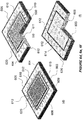
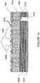
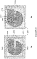
- the top contact comprises a continuous metallization layer having emission windows 1308 (only one labeled for clarity) created by selective etching (or selective deposition).
- the metallization between the windows form the top metal contact pads 1307 (only one labeled) for making electrical connections.
- Each window (1308) is aligned with a corresponding current confinement aperture of a VCSEL located directly below.
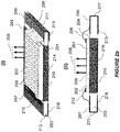
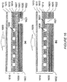
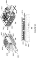
- the embodiment shown in Figure 18a comprises an array chip section 1800 and carrier substrate section 1810.
- the array chip section is substantially similar to the one described in reference with Figure 15a . That description will not be repeated.
- the carrier substrate 1810 comprises a substrate 1811 having one side coated with an antireflection layer 1812.
- a metallization layer 1814 having windows aligned with the chip array windows 1808 is disposed on the antireflection layer proximal to the array chip.
- the metallization layer surrounding the windows forming metal pads are used to bond the sections 1810 and 1800.
- the height at which microlenses are disposed above the array chip may be pre-determined and precisely controlled by the thickness of the carrier substrate 1811 for example, such that individual emissions from adjacent VCSELs each collimated using a corresponding microlens, fill up the dark space between the adjacent emissions. As a result, overall emission from the entire array module is distributed uniformly even at considerably large distance away from the array module.
- This embodiment may be particularly suitable for an application where an array module is configured to pump a solid state gain medium as described in United States Patent Application No. 13,369,581, van Leeuwen et al., filed February 09, 2012 .
- the embodiments shown in Figures 21 , 22 and 23 are described to have the array chips connected in series. This configuration is particularly suitable for low electrical current operation of the array module, yet delivering high optical output power.
- the array modules may be first constructed on a common substrate with appropriate electrical connections between each array chip, either in series or in parallel, according to the output optical power requirement. The combined array module may then be bonded to a single transparent carrier substrate all at once. Alternatively, and in particular for array modules connected in parallel, individual array modules may be connected separately one by one or in smaller groups, to the carrier substrate. These different choices have been described earlier with reference to Figure 19 .
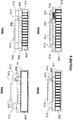
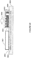
- FIG. 27 An exemplary embodiment to explain the principles of a simple stand-alone illuminator module is shown in Figure 27 . More specifically, a schematic view 2700 depicts a planar view of the illuminator module including a surface mountable array module 2702 and an electronic circuit 2721, respectively.
- the surface mountable array module 2702 may be similar to the one described in reference with Figures 15 , 16 , 17 , 18 and 19 , or may be a surface mountable array chip, similar to the ones described in reference with Figures 13a-13d .
- the electronic circuit in this particular example is a current driver to power the array module.
Landscapes
- Physics & Mathematics (AREA)
- Engineering & Computer Science (AREA)
- General Engineering & Computer Science (AREA)
- Condensed Matter Physics & Semiconductors (AREA)
- General Physics & Mathematics (AREA)
- Electromagnetism (AREA)
- Optics & Photonics (AREA)
- Semiconductor Lasers (AREA)
- Optical Couplings Of Light Guides (AREA)
- Arrangement Of Elements, Cooling, Sealing, Or The Like Of Lighting Devices (AREA)
Applications Claiming Priority (3)
| Application Number | Priority Date | Filing Date | Title |
|---|---|---|---|
| US13/337,098 US20130163627A1 (en) | 2011-12-24 | 2011-12-24 | Laser Illuminator System |
| US13/541,906 US8675706B2 (en) | 2011-12-24 | 2012-07-05 | Optical illuminator |
| EP12198546.9A EP2610978B1 (fr) | 2011-12-24 | 2012-12-20 | Emballage pour montage en surface pour des lasers à émission par la surface à cavité verticale à grande vitesse |
Related Parent Applications (2)
| Application Number | Title | Priority Date | Filing Date |
|---|---|---|---|
| EP12198546.9A Division EP2610978B1 (fr) | 2011-12-24 | 2012-12-20 | Emballage pour montage en surface pour des lasers à émission par la surface à cavité verticale à grande vitesse |
| EP12198546.9A Division-Into EP2610978B1 (fr) | 2011-12-24 | 2012-12-20 | Emballage pour montage en surface pour des lasers à émission par la surface à cavité verticale à grande vitesse |
Publications (2)
| Publication Number | Publication Date |
|---|---|
| EP3255742A1 true EP3255742A1 (fr) | 2017-12-13 |
| EP3255742B1 EP3255742B1 (fr) | 2019-08-14 |
Family
ID=47747281
Family Applications (2)
| Application Number | Title | Priority Date | Filing Date |
|---|---|---|---|
| EP17179558.6A Active EP3255742B1 (fr) | 2011-12-24 | 2012-12-20 | Emballage à montage en surface pour lasers à émission en surface de cavité verticale à grande vitesse |
| EP12198546.9A Active EP2610978B1 (fr) | 2011-12-24 | 2012-12-20 | Emballage pour montage en surface pour des lasers à émission par la surface à cavité verticale à grande vitesse |
Family Applications After (1)
| Application Number | Title | Priority Date | Filing Date |
|---|---|---|---|
| EP12198546.9A Active EP2610978B1 (fr) | 2011-12-24 | 2012-12-20 | Emballage pour montage en surface pour des lasers à émission par la surface à cavité verticale à grande vitesse |
Country Status (3)
| Country | Link |
|---|---|
| US (2) | US8675706B2 (fr) |
| EP (2) | EP3255742B1 (fr) |
| CN (2) | CN108110619B (fr) |
Cited By (1)
| Publication number | Priority date | Publication date | Assignee | Title |
|---|---|---|---|---|
| CN110132875A (zh) * | 2019-05-27 | 2019-08-16 | 哈尔滨工业大学 | 基于多源脉冲激光信息融合的弥散介质多宗量场重建装置及方法 |
Families Citing this family (177)
| Publication number | Priority date | Publication date | Assignee | Title |
|---|---|---|---|---|
| US9375300B2 (en) | 2012-02-02 | 2016-06-28 | Align Technology, Inc. | Identifying forces on a tooth |
| US9220580B2 (en) | 2012-03-01 | 2015-12-29 | Align Technology, Inc. | Determining a dental treatment difficulty |
| US9414897B2 (en) | 2012-05-22 | 2016-08-16 | Align Technology, Inc. | Adjustment of tooth position in a virtual dental model |
| US9706655B2 (en) * | 2013-07-09 | 2017-07-11 | Oleson Convergent Solutions Llc | Packaging for high power integrated circuits and infrared emitter arrays |
| US20150260830A1 (en) * | 2013-07-12 | 2015-09-17 | Princeton Optronics Inc. | 2-D Planar VCSEL Source for 3-D Imaging |
| DE112014003371T5 (de) * | 2013-07-22 | 2016-04-07 | Murata Manufacturing Co., Ltd. | Oberflächenemitter-array |
| US9456201B2 (en) | 2014-02-10 | 2016-09-27 | Microsoft Technology Licensing, Llc | VCSEL array for a depth camera |
| IL232197B (en) | 2014-04-23 | 2018-04-30 | Lumus Ltd | Compact head-up display system |
| US9577406B2 (en) | 2014-06-27 | 2017-02-21 | Microsoft Technology Licensing, Llc | Edge-emitting laser diode package comprising heat spreader |
| US9261356B2 (en) | 2014-07-03 | 2016-02-16 | Align Technology, Inc. | Confocal surface topography measurement with fixed focal positions |
| US9261358B2 (en) | 2014-07-03 | 2016-02-16 | Align Technology, Inc. | Chromatic confocal system |
| US9439568B2 (en) | 2014-07-03 | 2016-09-13 | Align Technology, Inc. | Apparatus and method for measuring surface topography optically |
| US10772506B2 (en) | 2014-07-07 | 2020-09-15 | Align Technology, Inc. | Apparatus for dental confocal imaging |
| US9693839B2 (en) | 2014-07-17 | 2017-07-04 | Align Technology, Inc. | Probe head and apparatus for intraoral confocal imaging using polarization-retarding coatings |
| US9675430B2 (en) | 2014-08-15 | 2017-06-13 | Align Technology, Inc. | Confocal imaging apparatus with curved focal surface |
| US9660418B2 (en) | 2014-08-27 | 2017-05-23 | Align Technology, Inc. | VCSEL based low coherence emitter for confocal 3D scanner |
| US10449016B2 (en) | 2014-09-19 | 2019-10-22 | Align Technology, Inc. | Arch adjustment appliance |
| US9610141B2 (en) | 2014-09-19 | 2017-04-04 | Align Technology, Inc. | Arch expanding appliance |
| US10028408B2 (en) * | 2014-10-15 | 2018-07-17 | Ge Aviation Systems Llc | Air agitator assemblies |
| US10359035B2 (en) * | 2014-10-15 | 2019-07-23 | Ge Aviation Systems Llc | Air agitator assemblies |
| CN107039882B (zh) * | 2014-10-28 | 2020-07-17 | 住友电气工业株式会社 | 应用光源、光调制器和输入单元的光学模块 |
| PL3219360T3 (pl) * | 2014-11-10 | 2020-10-19 | Sanhe Laserconn Tech Co., Ltd. | Urządzenie do zabiegów z laserem vcsel dużej mocy z funkcją chłodzenia skóry i jego struktura montażowa |
| US9744001B2 (en) | 2014-11-13 | 2017-08-29 | Align Technology, Inc. | Dental appliance with cavity for an unerupted or erupting tooth |
| US10504386B2 (en) | 2015-01-27 | 2019-12-10 | Align Technology, Inc. | Training method and system for oral-cavity-imaging-and-modeling equipment |
| WO2016190919A2 (fr) * | 2015-01-30 | 2016-12-01 | University Of Southern California | Microlasers à cavité verticale émettant par la surface (vcsel) dans des ensembles composites flexibles mis au point thermiquement |
| US9507430B2 (en) * | 2015-02-16 | 2016-11-29 | Lite-On Singapore Pte. Ltd. | Gesture sensing module |
| JP2016225527A (ja) * | 2015-06-02 | 2016-12-28 | 株式会社リコー | レーザ発光装置、エンジン点火プラグシステム |
| US10248883B2 (en) | 2015-08-20 | 2019-04-02 | Align Technology, Inc. | Photograph-based assessment of dental treatments and procedures |
| CN108027129B (zh) * | 2015-08-28 | 2020-05-15 | 赫普塔冈微光有限公司 | 用于平移光的照明模块 |
| US10135218B2 (en) | 2015-10-02 | 2018-11-20 | Ayar Labs, Inc. | Multi-wavelength laser system for optical data communication links and associated methods |
| CN108604053B (zh) | 2015-10-21 | 2021-11-02 | 普林斯顿光电子股份有限公司 | 编码图案投影仪 |
| US11931222B2 (en) | 2015-11-12 | 2024-03-19 | Align Technology, Inc. | Dental attachment formation structures |
| US11554000B2 (en) | 2015-11-12 | 2023-01-17 | Align Technology, Inc. | Dental attachment formation structure |
| US11596502B2 (en) | 2015-12-09 | 2023-03-07 | Align Technology, Inc. | Dental attachment placement structure |
| US11103330B2 (en) | 2015-12-09 | 2021-08-31 | Align Technology, Inc. | Dental attachment placement structure |
| US10257932B2 (en) * | 2016-02-16 | 2019-04-09 | Microsoft Technology Licensing, Llc. | Laser diode chip on printed circuit board |
| US9837792B2 (en) * | 2016-03-07 | 2017-12-05 | Epistar Corporation | Light-emitting device |
| US10761195B2 (en) | 2016-04-22 | 2020-09-01 | OPSYS Tech Ltd. | Multi-wavelength LIDAR system |
| JP6880855B2 (ja) * | 2016-05-17 | 2021-06-02 | セイコーエプソン株式会社 | 光源装置およびプロジェクター |
| EP3465845B1 (fr) * | 2016-06-03 | 2023-01-11 | Princeton Optronics, Inc. | Boîtier d'illuminateur à laser vcsel |
| EP3471599B1 (fr) | 2016-06-17 | 2025-11-19 | Align Technology, Inc. | Appareils intraoraux avec détection |
| WO2017218951A1 (fr) | 2016-06-17 | 2017-12-21 | Align Technology, Inc. | Dispositif de surveillance de performances d'un appareil orthodontique |
| US10072815B2 (en) | 2016-06-23 | 2018-09-11 | Apple Inc. | Top-emission VCSEL-array with integrated diffuser |
| FR3054381B1 (fr) * | 2016-07-19 | 2018-11-16 | Sidel Participations | Emetteur laser a haute densite energetique |
| WO2018022940A1 (fr) | 2016-07-27 | 2018-02-01 | Align Technology, Inc. | Scanner intra-buccal pouvant établir un diagnostic dentaire |
| US10507087B2 (en) | 2016-07-27 | 2019-12-17 | Align Technology, Inc. | Methods and apparatuses for forming a three-dimensional volumetric model of a subject's teeth |
| JP6747910B2 (ja) | 2016-08-10 | 2020-08-26 | 浜松ホトニクス株式会社 | 発光装置 |
| US11031751B2 (en) | 2016-08-10 | 2021-06-08 | Hamamatsu Photonics K.K. | Light-emitting device |
| US10734786B2 (en) * | 2016-09-07 | 2020-08-04 | Hamamatsu Photonics K.K. | Semiconductor light emitting element and light emitting device including same |
| JP7187022B2 (ja) | 2016-10-09 | 2022-12-12 | ルムス エルティーディー. | 長方形導波路を使用する開口乗算器 |
| US10595966B2 (en) | 2016-11-04 | 2020-03-24 | Align Technology, Inc. | Methods and apparatuses for dental images |
| CN113031165B (zh) | 2016-11-08 | 2023-06-02 | 鲁姆斯有限公司 | 导光装置、其光学组件及其对应的生产方法 |
| US11026831B2 (en) | 2016-12-02 | 2021-06-08 | Align Technology, Inc. | Dental appliance features for speech enhancement |
| EP3547950A1 (fr) | 2016-12-02 | 2019-10-09 | Align Technology, Inc. | Procédés et appareils pour personnaliser des dispositifs d'expansion palatine rapides à l'aide de modèles numériques |
| CN114224534B (zh) | 2016-12-02 | 2025-02-18 | 阿莱恩技术有限公司 | 腭扩张器和扩张腭的方法 |
| US11376101B2 (en) | 2016-12-02 | 2022-07-05 | Align Technology, Inc. | Force control, stop mechanism, regulating structure of removable arch adjustment appliance |
| US10548700B2 (en) | 2016-12-16 | 2020-02-04 | Align Technology, Inc. | Dental appliance etch template |
| DE102016125430A1 (de) * | 2016-12-22 | 2018-06-28 | Osram Opto Semiconductors Gmbh | Oberflächenmontierbarer Halbleiterlaser, Anordnung mit einem solchen Halbleiterlaser und Betriebsverfahren hierfür |
| US10714892B2 (en) * | 2017-01-10 | 2020-07-14 | Ii-Vi Delaware Inc. | Light sources with chip-level integrated diffusers |
| US10456043B2 (en) | 2017-01-12 | 2019-10-29 | Align Technology, Inc. | Compact confocal dental scanning apparatus |
| CN110214380B (zh) | 2017-01-25 | 2024-04-09 | 苏州立琻半导体有限公司 | 半导体器件 |
| WO2018147963A1 (fr) | 2017-02-08 | 2018-08-16 | Princeton Optronics, Inc. | Boîtier d'éclairage vcsel comprenant une structure optique intégrée dans l'encapsulant |
| US10779718B2 (en) | 2017-02-13 | 2020-09-22 | Align Technology, Inc. | Cheek retractor and mobile device holder |
| CN111133641A (zh) * | 2017-02-24 | 2020-05-08 | 普林斯顿光电子公司 | 人眼安全vcsel照明器封装件 |
| CN110402398B (zh) | 2017-03-13 | 2023-12-01 | 欧普赛斯技术有限公司 | 眼睛安全的扫描激光雷达系统 |
| JP7089504B2 (ja) * | 2017-03-27 | 2022-06-22 | 浜松ホトニクス株式会社 | 半導体発光素子およびその製造方法 |
| US11637409B2 (en) * | 2017-03-27 | 2023-04-25 | Hamamatsu Photonics K.K. | Semiconductor light-emitting module and control method therefor |
| WO2018183358A1 (fr) | 2017-03-27 | 2018-10-04 | Align Technology, Inc. | Appareils et procédés d'aide à des thérapies dentaires |
| US11646546B2 (en) | 2017-03-27 | 2023-05-09 | Hamamatsu Photonics K.K. | Semiconductor light emitting array with phase modulation regions for generating beam projection patterns |
| EP3382828A1 (fr) * | 2017-03-31 | 2018-10-03 | Koninklijke Philips N.V. | Agencement de laser à sécurité intrinsèque comprenant un laser à cavité verticale émettant en surface |
| US10613515B2 (en) | 2017-03-31 | 2020-04-07 | Align Technology, Inc. | Orthodontic appliances including at least partially un-erupted teeth and method of forming them |
| WO2018191489A1 (fr) * | 2017-04-12 | 2018-10-18 | Sense Photonics, Inc. | Laser à émission de surface à cavité verticale ultra-petite (vcsel) et réseaux l'incorporant |
| US10535799B2 (en) | 2017-05-09 | 2020-01-14 | Epistar Corporation | Semiconductor device |
| US11045283B2 (en) | 2017-06-09 | 2021-06-29 | Align Technology, Inc. | Palatal expander with skeletal anchorage devices |
| JP6959042B2 (ja) | 2017-06-15 | 2021-11-02 | 浜松ホトニクス株式会社 | 発光装置 |
| CN116942335A (zh) | 2017-06-16 | 2023-10-27 | 阿莱恩技术有限公司 | 牙齿类型和萌出状态的自动检测 |
| US10639134B2 (en) | 2017-06-26 | 2020-05-05 | Align Technology, Inc. | Biosensor performance indicator for intraoral appliances |
| US10885521B2 (en) | 2017-07-17 | 2021-01-05 | Align Technology, Inc. | Method and apparatuses for interactive ordering of dental aligners |
| JP7174929B2 (ja) | 2017-07-19 | 2022-11-18 | ルムス エルティーディー. | Loeを介するlcos照明 |
| WO2019018784A1 (fr) | 2017-07-21 | 2019-01-24 | Align Technology, Inc. | Ancrage de contour palatin |
| US11482835B2 (en) * | 2017-07-25 | 2022-10-25 | Lumentum Operations Llc | VCSEL device with multiple stacked active regions |
| WO2019023401A1 (fr) | 2017-07-25 | 2019-01-31 | Trilumina Corp. | Réseau de lasers vcsel connecté en série à une seule puce |
| WO2019023461A1 (fr) | 2017-07-27 | 2019-01-31 | Align Technology, Inc. | Teinte, transparence et émaillage dentaire |
| CN110996836B (zh) | 2017-07-27 | 2023-04-11 | 阿莱恩技术有限公司 | 用于通过光学相干断层扫描术来处理正畸矫正器的系统和方法 |
| US10514444B2 (en) | 2017-07-28 | 2019-12-24 | OPSYS Tech Ltd. | VCSEL array LIDAR transmitter with small angular divergence |
| CN107492786B (zh) * | 2017-08-08 | 2019-04-30 | 温惟善 | 一种smd小型化封装的vcsel制造工艺 |
| US12274597B2 (en) * | 2017-08-11 | 2025-04-15 | Align Technology, Inc. | Dental attachment template tray systems |
| WO2019035979A1 (fr) | 2017-08-15 | 2019-02-21 | Align Technology, Inc. | Évaluation et calcul de couloir buccal |
| WO2019036677A1 (fr) | 2017-08-17 | 2019-02-21 | Align Technology, Inc. | Surveillance de conformité d'appareil dentaire |
| CN111213294B (zh) * | 2017-08-22 | 2023-05-05 | 普林斯顿光电子公司 | 用于高密度光发射器阵列的多层导体互连件 |
| US12171575B2 (en) | 2017-10-04 | 2024-12-24 | Align Technology, Inc. | Intraoral systems and methods for sampling soft-tissue |
| US10813720B2 (en) | 2017-10-05 | 2020-10-27 | Align Technology, Inc. | Interproximal reduction templates |
| WO2019084326A1 (fr) | 2017-10-27 | 2019-05-02 | Align Technology, Inc. | Autres structures de réglage de morsure |
| CN116602778A (zh) | 2017-10-31 | 2023-08-18 | 阿莱恩技术有限公司 | 具有选择性牙合负荷和受控牙尖交错的牙科器具 |
| EP3703607B1 (fr) | 2017-11-01 | 2025-03-26 | Align Technology, Inc. | Planification automatique de traitement |
| CN109756652B (zh) * | 2017-11-01 | 2021-02-05 | 浙江舜宇智能光学技术有限公司 | Tof摄像模组及其制造方法 |
| US10638643B2 (en) * | 2017-11-14 | 2020-04-28 | Canon Kabushiki Kaisha | Electronic device |
| KR102634870B1 (ko) | 2017-11-15 | 2024-02-13 | 옵시스 테크 엘티디 | 잡음 적응형 솔리드-스테이트 lidar 시스템 |
| US11534974B2 (en) | 2017-11-17 | 2022-12-27 | Align Technology, Inc. | Customized fabrication of orthodontic retainers based on patient anatomy |
| CN118948478A (zh) | 2017-11-30 | 2024-11-15 | 阿莱恩技术有限公司 | 用于监测口腔矫治器的传感器 |
| DE112018006285T5 (de) | 2017-12-08 | 2021-01-28 | Hamamatsu Photonics K.K. | Lichtemittierende vorrichtung und herstellungsverfahren dafür |
| WO2019118876A1 (fr) | 2017-12-15 | 2019-06-20 | Align Technology, Inc. | Méthodes et appareils de traitement orthodontique adaptatif à boucle fermée |
| US20210057888A1 (en) * | 2017-12-28 | 2021-02-25 | Princeton Optronics, Inc. | Structured light projection system including narrow beam divergence semiconductor sources |
| US10980613B2 (en) | 2017-12-29 | 2021-04-20 | Align Technology, Inc. | Augmented reality enhancements for dental practitioners |
| US11283240B2 (en) * | 2018-01-09 | 2022-03-22 | Oepic Semiconductors, Inc. | Pillar confined backside emitting VCSEL |
| US11233377B2 (en) * | 2018-01-26 | 2022-01-25 | Oepic Semiconductors Inc. | Planarization of backside emitting VCSEL and method of manufacturing the same for array application |
| US11264780B2 (en) * | 2018-01-26 | 2022-03-01 | Oepic Semiconductors, Inc. | Flip chip backside emitting VCSEL package |
| JP7427595B2 (ja) | 2018-01-26 | 2024-02-05 | アライン テクノロジー, インコーポレイテッド | 診断の為の口腔内のスキャン及び追跡 |
| US11937991B2 (en) | 2018-03-27 | 2024-03-26 | Align Technology, Inc. | Dental attachment placement structure |
| JP7324518B2 (ja) | 2018-04-01 | 2023-08-10 | オプシス テック リミテッド | 雑音適応型固体ライダシステム |
| WO2019200008A1 (fr) | 2018-04-11 | 2019-10-17 | Align Technology, Inc. | Appareils d'expansion palatine libérables |
| EP3783759B1 (fr) | 2018-04-19 | 2024-05-01 | Sony Semiconductor Solutions Corporation | Dispositif de pilotage de laser à semi-conducteur et son procédé de fabrication |
| CN110456367A (zh) * | 2018-05-07 | 2019-11-15 | 光宝新加坡有限公司 | 具有双发射器的近接感应模块 |
| IL259518B2 (en) | 2018-05-22 | 2023-04-01 | Lumus Ltd | Optical system and method for improving light field uniformity |
| US10700780B2 (en) | 2018-05-30 | 2020-06-30 | Apple Inc. | Systems and methods for adjusting movable lenses in directional free-space optical communication systems for portable electronic devices |
| US10705347B2 (en) | 2018-05-30 | 2020-07-07 | Apple Inc. | Wafer-level high aspect ratio beam shaping |
| US11303355B2 (en) | 2018-05-30 | 2022-04-12 | Apple Inc. | Optical structures in directional free-space optical communication systems for portable electronic devices |
| US10374386B1 (en) * | 2018-06-07 | 2019-08-06 | Finisar Corporation | Chip on carrier |
| CN112272906B (zh) | 2018-06-08 | 2024-03-15 | 浜松光子学株式会社 | 发光元件 |
| EP3588700A1 (fr) * | 2018-06-26 | 2020-01-01 | Koninklijke Philips N.V. | Dispositif vcsel pour un capteur smi pour l'enregistrement d'images tridimensionnelles |
| US11415812B2 (en) | 2018-06-26 | 2022-08-16 | Lumus Ltd. | Compact collimating optical device and system |
| CN108919597B (zh) * | 2018-07-30 | 2024-02-13 | 深圳阜时科技有限公司 | 一种光学投影模组 |
| CN112543875B (zh) | 2018-08-03 | 2024-12-13 | 欧普赛斯技术有限公司 | 分布式模块化固态lidar系统 |
| US11073615B2 (en) * | 2018-08-20 | 2021-07-27 | Lite-On Singapore Pte. Ltd. | Proximity sensor module with two sensors |
| US20210194212A1 (en) * | 2018-08-30 | 2021-06-24 | Ams Sensors Asia Pte. Ltd. | Vcsels including a sub-wavelength grating for wavelength locking |
| US11178392B2 (en) | 2018-09-12 | 2021-11-16 | Apple Inc. | Integrated optical emitters and applications thereof |
| WO2020061752A1 (fr) * | 2018-09-25 | 2020-04-02 | Shenzhen Raysees Technology Co., Ltd. | Réseau de lasers à émission par la surface (vcsel) et procédé de fabrication |
| WO2020093275A1 (fr) * | 2018-11-07 | 2020-05-14 | Shenzhen Raysees Technology Co., Ltd. | Système et procédé destinés à éviter des défaillances induites thermiquement dans un réseau laser à cavité verticale émettant par la surface (vcsel) |
| TWI701882B (zh) * | 2018-11-08 | 2020-08-11 | 晶智達光電股份有限公司 | 雷射元件 |
| JP7353299B2 (ja) * | 2018-11-20 | 2023-09-29 | ソニーセミコンダクタソリューションズ株式会社 | 発光デバイス及び発光装置 |
| US11137246B2 (en) * | 2019-01-31 | 2021-10-05 | Himax Technologies Limited | Optical device |
| CN113557644B (zh) | 2019-02-04 | 2024-03-29 | 苹果公司 | 具有一体式微透镜的竖直发射器 |
| JP7293697B2 (ja) | 2019-02-06 | 2023-06-20 | 富士フイルムビジネスイノベーション株式会社 | 発光装置、光学装置および情報処理装置 |
| US11764544B2 (en) * | 2019-02-28 | 2023-09-19 | Seoul Viosys Co., Ltd. | Vertical-cavity surface-emitting laser |
| WO2020183229A1 (fr) | 2019-03-12 | 2020-09-17 | Lumus Ltd. | Projecteur d'image |
| JP2020155622A (ja) * | 2019-03-20 | 2020-09-24 | 富士ゼロックス株式会社 | 発光装置、光学装置および情報処理装置 |
| JP7512570B2 (ja) * | 2019-03-20 | 2024-07-09 | 富士フイルムビジネスイノベーション株式会社 | 発光装置、光学装置および情報処理装置 |
| WO2020202120A1 (fr) | 2019-04-04 | 2020-10-08 | Lumus Ltd. | Dispositif d'affichage proche de l'oeil perpendiculaire sans entrefer |
| KR102634887B1 (ko) | 2019-04-09 | 2024-02-08 | 옵시스 테크 엘티디 | 레이저 제어를 갖는 솔리드-스테이트 lidar 송신기 |
| CN110137803A (zh) * | 2019-05-26 | 2019-08-16 | 杭州晟创激光科技有限公司 | 一种激光器(vcsel)封装结构 |
| KR20220003600A (ko) | 2019-05-30 | 2022-01-10 | 옵시스 테크 엘티디 | 액추에이터를 사용하는 눈-안전 장거리 lidar 시스템 |
| KR102580722B1 (ko) | 2019-06-10 | 2023-09-22 | 옵시스 테크 엘티디 | 눈-안전 장거리 고체 상태 lidar 시스템 |
| WO2020263735A1 (fr) | 2019-06-25 | 2020-12-30 | OPSYS Tech Ltd. | Système lidar adaptatif à impulsions multiples |
| CN114008877B (zh) * | 2019-06-27 | 2024-06-18 | ams传感器亚洲私人有限公司 | 结合增强安全特征和热管理的发光模块 |
| US11549799B2 (en) | 2019-07-01 | 2023-01-10 | Apple Inc. | Self-mixing interference device for sensing applications |
| CN114175425A (zh) * | 2019-07-30 | 2022-03-11 | 索尼半导体解决方案公司 | 半导体激光驱动装置、电子设备和半导体激光驱动装置的制造方法 |
| US12222445B2 (en) | 2019-07-31 | 2025-02-11 | OPSYS Tech Ltd. | High-resolution solid-state LIDAR transmitter |
| CN110596675A (zh) * | 2019-08-21 | 2019-12-20 | 深圳奥锐达科技有限公司 | 一种激光发射装置及激光雷达系统 |
| EP4024631A4 (fr) * | 2019-08-28 | 2023-09-20 | SOS LAB Co., Ltd | Réseau vcsel et dispositif lidar l'utilisant |
| KR102873358B1 (ko) * | 2019-08-28 | 2025-10-21 | 주식회사 에스오에스랩 | 거리 측정 장치 |
| KR102893003B1 (ko) | 2019-09-16 | 2025-11-27 | 루머스 리미티드 | 헤드 마운트 디스플레이용 컴팩트 프로젝터 |
| US20220344899A1 (en) * | 2019-09-18 | 2022-10-27 | Osram Opto Semiconductors Gmbh | Optoelectronic semiconductor chip comprising a contact element and method of manufacturing an optoelectronic semiconductor chip |
| JP7400282B2 (ja) * | 2019-09-18 | 2023-12-19 | 株式会社リコー | 面発光レーザ、面発光レーザ装置、光源装置及び検出装置 |
| CA3155597C (fr) | 2019-12-08 | 2023-02-14 | Lumus Ltd. | Systeme optique avec projecteur d'image compact |
| CN111029901B (zh) * | 2019-12-11 | 2021-06-29 | 深圳博升光电科技有限公司 | 垂直腔面发射激光器的结构及制造方法 |
| DE102019220075A1 (de) * | 2019-12-18 | 2021-06-24 | Robert Bosch Gmbh | Optisches Element |
| JP7518173B2 (ja) * | 2020-01-17 | 2024-07-17 | エイエムエス-オスラム エイジア パシフィック プライヴェット リミテッド | 線形光学装置 |
| CN111276865B (zh) * | 2020-02-19 | 2024-09-06 | 松山湖材料实验室 | Ld白光装置及其制备方法 |
| CN111293584B (zh) * | 2020-02-20 | 2021-04-16 | 浙江博升光电科技有限公司 | 多层多区垂直腔面发射激光器装置 |
| JP7521203B2 (ja) | 2020-02-26 | 2024-07-24 | 富士フイルムビジネスイノベーション株式会社 | 発光装置、光学装置及び計測装置 |
| JP2021141257A (ja) * | 2020-03-06 | 2021-09-16 | ソニーセミコンダクタソリューションズ株式会社 | 発光装置およびその製造方法 |
| JP7480545B2 (ja) * | 2020-03-24 | 2024-05-10 | 富士フイルムビジネスイノベーション株式会社 | 発光装置、光学装置、計測装置及び情報処理装置 |
| WO2021196368A1 (fr) * | 2020-04-02 | 2021-10-07 | Shenzhen Raysees AI Technology Co., Ltd. | Réseau vcsel à jonctions multiples à émission par le bas |
| CN115516721A (zh) | 2020-05-10 | 2022-12-23 | 苹果公司 | 折叠的光学共轭透镜 |
| WO2021235143A1 (fr) * | 2020-05-21 | 2021-11-25 | ソニーセミコンダクタソリューションズ株式会社 | Dispositif électronique |
| KR102925263B1 (ko) * | 2020-06-25 | 2026-02-09 | 엘지이노텍 주식회사 | 표면 발광 레이저 소자 및 vcsel 모듈 |
| CN116325390B (zh) * | 2020-10-20 | 2025-04-08 | 三菱电机株式会社 | 光半导体装置 |
| JP2024004500A (ja) * | 2020-11-19 | 2024-01-17 | ソニーセミコンダクタソリューションズ株式会社 | 半導体装置 |
| US11994694B2 (en) | 2021-01-17 | 2024-05-28 | Apple Inc. | Microlens array with tailored sag profile |
| JP7683252B2 (ja) * | 2021-03-12 | 2025-05-27 | 株式会社リコー | 面発光レーザアレイ、光源モジュール及び測距装置 |
| KR20230040823A (ko) * | 2021-09-16 | 2023-03-23 | 엘지이노텍 주식회사 | 카메라 모듈 및 이를 포함하는 광학기기 |
| US12413043B2 (en) | 2021-09-21 | 2025-09-09 | Apple Inc. | Self-mixing interference device with tunable microelectromechanical system |
| US20230254556A1 (en) * | 2022-02-04 | 2023-08-10 | Zimeno, Inc. Dba Monarch Tractor | Sensor maintenance |
| CN115133392A (zh) * | 2022-06-20 | 2022-09-30 | 深圳市聚飞光电股份有限公司 | 一种光源投射器、3d传感器以及电子设备 |
| CN115377802A (zh) * | 2022-08-18 | 2022-11-22 | 西安炬光科技股份有限公司 | 线光斑光源发射装置和设备 |
| US12613131B2 (en) | 2022-09-22 | 2026-04-28 | Apple Inc. | Optical proximity sensor |
| US12601583B2 (en) | 2023-05-17 | 2026-04-14 | Apple Inc. | Multi-channel self-mixing interferometric sensor |
Citations (4)
| Publication number | Priority date | Publication date | Assignee | Title |
|---|---|---|---|---|
| EP0975072A2 (fr) * | 1998-07-22 | 2000-01-26 | Canon Kabushiki Kaisha | Dispositif ayant une fonction optique avec des électrodes d'interconnexion spéciales et méthode de fabrication |
| EP1653523A2 (fr) * | 2004-10-28 | 2006-05-03 | LumiLeds Lighting U.S., LLC | Boîtier de diode électroluminescente |
| US20070085101A1 (en) * | 2005-10-19 | 2007-04-19 | Lg Innotek Co., Ltd. | Light emitting diode package |
| EP2128939A2 (fr) * | 2008-05-29 | 2009-12-02 | Ricoh Company, Ltd. | Appareil luminescent, appareil de balayage optique et appareil de formation d'images |
Family Cites Families (25)
| Publication number | Priority date | Publication date | Assignee | Title |
|---|---|---|---|---|
| US5266794A (en) * | 1992-01-21 | 1993-11-30 | Bandgap Technology Corporation | Vertical-cavity surface emitting laser optical interconnect technology |
| JPH08293641A (ja) * | 1995-04-24 | 1996-11-05 | Mitsubishi Electric Corp | 半導体レーザアレイ装置 |
| US5946121A (en) | 1996-07-02 | 1999-08-31 | Motorola, Inc. | IrDA data link with VCSEL light source |
| US6780661B1 (en) * | 2000-04-12 | 2004-08-24 | Finisar Corporation | Integration of top-emitting and top-illuminated optoelectronic devices with micro-optic and electronic integrated circuits |
| DE10129743C2 (de) | 2001-06-20 | 2003-05-08 | Daimler Chrysler Ag | Fahrzeugscheinwerfer, mit einer Anzahl von elektronischen Leuchtelementen als Lichtquelle |
| US20030026310A1 (en) | 2001-08-06 | 2003-02-06 | Motorola, Inc. | Structure and method for fabrication for a lighting device |
| US20030185499A1 (en) | 2002-04-02 | 2003-10-02 | Edward Butler | High speed optical interconnects |
| AU2003298561A1 (en) * | 2002-08-23 | 2004-05-13 | Jonathan S. Dahm | Method and apparatus for using light emitting diodes |
| US6950454B2 (en) | 2003-03-24 | 2005-09-27 | Eastman Kodak Company | Electronic imaging system using organic laser array illuminating an area light valve |
| JP2005079385A (ja) * | 2003-09-01 | 2005-03-24 | Toshiba Corp | 光半導体装置および光信号入出力装置 |
| US6984076B2 (en) * | 2003-10-08 | 2006-01-10 | Honeywell International Inc. | Compact package design for vertical cavity surface emitting laser array to optical fiber cable connection |
| EP1800255A4 (fr) | 2004-10-15 | 2012-06-06 | Auto Sense Llc | Systeme de detection d'objets a reseau de diodes vcsel |
| US8412052B2 (en) | 2004-10-22 | 2013-04-02 | Intel Corporation | Surface mount (SMT) connector for VCSEL and photodiode arrays |
| JP4844031B2 (ja) | 2005-07-20 | 2011-12-21 | 富士ゼロックス株式会社 | 発光モジュール |
| JP4708214B2 (ja) * | 2006-02-23 | 2011-06-22 | 浜松ホトニクス株式会社 | 光送受信デバイス |
| US7949022B2 (en) | 2006-04-27 | 2011-05-24 | Lockheed Martin Corporation | Diode pumping of a laser gain medium |
| US20080079904A1 (en) | 2006-09-30 | 2008-04-03 | Texas Instruments Incorporated | Display systems with spatial light modulators |
| US8315526B2 (en) | 2007-06-18 | 2012-11-20 | Hewlett-Packard Development Company, L.P. | Misalignment tolerant free space optical transceiver |
| JP5212686B2 (ja) * | 2007-08-22 | 2013-06-19 | ソニー株式会社 | 半導体レーザアレイの製造方法 |
| KR101426285B1 (ko) * | 2008-01-09 | 2014-08-05 | 삼성전자주식회사 | 광 송수신 소자 및 그 제조방법 |
| JP5439953B2 (ja) * | 2008-10-30 | 2014-03-12 | ソニー株式会社 | 半導体レーザおよびその製造方法 |
| JP2011029339A (ja) * | 2009-07-23 | 2011-02-10 | Sony Corp | 半導体素子およびその製造方法 |
| US8111730B2 (en) * | 2009-08-20 | 2012-02-07 | International Business Machines Corporation | 3D optoelectronic packaging |
| CN101895057A (zh) * | 2010-05-24 | 2010-11-24 | 中国科学院长春光学精密机械与物理研究所 | 一种互注入锁定的二维表面发射激光器阵列 |
| US20120087385A1 (en) | 2010-10-08 | 2012-04-12 | Oakes David B | Flare for battlefield illumination |
-
2012
- 2012-07-05 US US13/541,906 patent/US8675706B2/en active Active
- 2012-12-20 EP EP17179558.6A patent/EP3255742B1/fr active Active
- 2012-12-20 EP EP12198546.9A patent/EP2610978B1/fr active Active
- 2012-12-21 CN CN201810061235.XA patent/CN108110619B/zh active Active
- 2012-12-21 CN CN201210563102.5A patent/CN103178442B/zh active Active
-
2014
- 2014-01-28 US US14/166,664 patent/US8783893B1/en active Active
Patent Citations (4)
| Publication number | Priority date | Publication date | Assignee | Title |
|---|---|---|---|---|
| EP0975072A2 (fr) * | 1998-07-22 | 2000-01-26 | Canon Kabushiki Kaisha | Dispositif ayant une fonction optique avec des électrodes d'interconnexion spéciales et méthode de fabrication |
| EP1653523A2 (fr) * | 2004-10-28 | 2006-05-03 | LumiLeds Lighting U.S., LLC | Boîtier de diode électroluminescente |
| US20070085101A1 (en) * | 2005-10-19 | 2007-04-19 | Lg Innotek Co., Ltd. | Light emitting diode package |
| EP2128939A2 (fr) * | 2008-05-29 | 2009-12-02 | Ricoh Company, Ltd. | Appareil luminescent, appareil de balayage optique et appareil de formation d'images |
Cited By (2)
| Publication number | Priority date | Publication date | Assignee | Title |
|---|---|---|---|---|
| CN110132875A (zh) * | 2019-05-27 | 2019-08-16 | 哈尔滨工业大学 | 基于多源脉冲激光信息融合的弥散介质多宗量场重建装置及方法 |
| CN110132875B (zh) * | 2019-05-27 | 2021-09-10 | 哈尔滨工业大学 | 基于多源脉冲激光信息融合的弥散介质多宗量场重建装置及方法 |
Also Published As
| Publication number | Publication date |
|---|---|
| US8675706B2 (en) | 2014-03-18 |
| CN108110619A (zh) | 2018-06-01 |
| CN103178442B (zh) | 2018-02-02 |
| EP3255742B1 (fr) | 2019-08-14 |
| US20130163626A1 (en) | 2013-06-27 |
| US20140218898A1 (en) | 2014-08-07 |
| EP2610978A2 (fr) | 2013-07-03 |
| CN108110619B (zh) | 2020-04-28 |
| US8783893B1 (en) | 2014-07-22 |
| CN103178442A (zh) | 2013-06-26 |
| EP2610978B1 (fr) | 2017-08-16 |
| EP2610978A3 (fr) | 2014-03-05 |
Similar Documents
| Publication | Publication Date | Title |
|---|---|---|
| EP3255742B1 (fr) | Emballage à montage en surface pour lasers à émission en surface de cavité verticale à grande vitesse | |
| US20130163627A1 (en) | Laser Illuminator System | |
| US9553423B2 (en) | Miniature structured light illuminator | |
| US9038883B2 (en) | VCSEL packaging | |
| US10290993B2 (en) | VCSEL illuminator package | |
| US11105899B2 (en) | Beam shaping for ultra-small vertical cavity surface emitting laser (VCSEL) arrays | |
| ES2758438T3 (es) | Módulo láser de diodo escalonado con estructura de refrigeración | |
| EP3292598B1 (fr) | Boîtier à diodes laser multi-émetteurs | |
| CN110537301B (zh) | 包括集成于包封物中的光学结构的vcsel照明器封装 | |
| US20160072258A1 (en) | High Resolution Structured Light Source | |
| CN111146690B (zh) | 一种激光器模组及其制备方法 | |
| CN111133641A (zh) | 人眼安全vcsel照明器封装件 | |
| US20210296852A1 (en) | Vertical cavity surface emitting laser (vcsel) array package and manufacturing method | |
| JP4877239B2 (ja) | 発光装置の製造方法 | |
| US20250379416A1 (en) | Laser package device and manufacturing method therefor and laser light source device | |
| US7789573B2 (en) | Optoelectronic module |
Legal Events
| Date | Code | Title | Description |
|---|---|---|---|
| PUAI | Public reference made under article 153(3) epc to a published international application that has entered the european phase |
Free format text: ORIGINAL CODE: 0009012 |
|
| STAA | Information on the status of an ep patent application or granted ep patent |
Free format text: STATUS: THE APPLICATION HAS BEEN PUBLISHED |
|
| AC | Divisional application: reference to earlier application |
Ref document number: 2610978 Country of ref document: EP Kind code of ref document: P |
|
| AK | Designated contracting states |
Kind code of ref document: A1 Designated state(s): AL AT BE BG CH CY CZ DE DK EE ES FI FR GB GR HR HU IE IS IT LI LT LU LV MC MK MT NL NO PL PT RO RS SE SI SK SM TR |
|
| STAA | Information on the status of an ep patent application or granted ep patent |
Free format text: STATUS: REQUEST FOR EXAMINATION WAS MADE |
|
| 17P | Request for examination filed |
Effective date: 20180613 |
|
| RBV | Designated contracting states (corrected) |
Designated state(s): AL AT BE BG CH CY CZ DE DK EE ES FI FR GB GR HR HU IE IS IT LI LT LU LV MC MK MT NL NO PL PT RO RS SE SI SK SM TR |
|
| GRAP | Despatch of communication of intention to grant a patent |
Free format text: ORIGINAL CODE: EPIDOSNIGR1 |
|
| STAA | Information on the status of an ep patent application or granted ep patent |
Free format text: STATUS: GRANT OF PATENT IS INTENDED |
|
| INTG | Intention to grant announced |
Effective date: 20190221 |
|
| GRAS | Grant fee paid |
Free format text: ORIGINAL CODE: EPIDOSNIGR3 |
|
| GRAA | (expected) grant |
Free format text: ORIGINAL CODE: 0009210 |
|
| STAA | Information on the status of an ep patent application or granted ep patent |
Free format text: STATUS: THE PATENT HAS BEEN GRANTED |
|
| AC | Divisional application: reference to earlier application |
Ref document number: 2610978 Country of ref document: EP Kind code of ref document: P |
|
| AK | Designated contracting states |
Kind code of ref document: B1 Designated state(s): AL AT BE BG CH CY CZ DE DK EE ES FI FR GB GR HR HU IE IS IT LI LT LU LV MC MK MT NL NO PL PT RO RS SE SI SK SM TR |
|
| REG | Reference to a national code |
Ref country code: GB Ref legal event code: FG4D |
|
| REG | Reference to a national code |
Ref country code: CH Ref legal event code: EP Ref country code: AT Ref legal event code: REF Ref document number: 1168136 Country of ref document: AT Kind code of ref document: T Effective date: 20190815 |
|
| REG | Reference to a national code |
Ref country code: IE Ref legal event code: FG4D |
|
| REG | Reference to a national code |
Ref country code: DE Ref legal event code: R096 Ref document number: 602012063049 Country of ref document: DE |
|
| REG | Reference to a national code |
Ref country code: NL Ref legal event code: MP Effective date: 20190814 |
|
| REG | Reference to a national code |
Ref country code: LT Ref legal event code: MG4D |
|
| PG25 | Lapsed in a contracting state [announced via postgrant information from national office to epo] |
Ref country code: PT Free format text: LAPSE BECAUSE OF FAILURE TO SUBMIT A TRANSLATION OF THE DESCRIPTION OR TO PAY THE FEE WITHIN THE PRESCRIBED TIME-LIMIT Effective date: 20191216 Ref country code: BG Free format text: LAPSE BECAUSE OF FAILURE TO SUBMIT A TRANSLATION OF THE DESCRIPTION OR TO PAY THE FEE WITHIN THE PRESCRIBED TIME-LIMIT Effective date: 20191114 Ref country code: NL Free format text: LAPSE BECAUSE OF FAILURE TO SUBMIT A TRANSLATION OF THE DESCRIPTION OR TO PAY THE FEE WITHIN THE PRESCRIBED TIME-LIMIT Effective date: 20190814 Ref country code: LT Free format text: LAPSE BECAUSE OF FAILURE TO SUBMIT A TRANSLATION OF THE DESCRIPTION OR TO PAY THE FEE WITHIN THE PRESCRIBED TIME-LIMIT Effective date: 20190814 Ref country code: HR Free format text: LAPSE BECAUSE OF FAILURE TO SUBMIT A TRANSLATION OF THE DESCRIPTION OR TO PAY THE FEE WITHIN THE PRESCRIBED TIME-LIMIT Effective date: 20190814 Ref country code: NO Free format text: LAPSE BECAUSE OF FAILURE TO SUBMIT A TRANSLATION OF THE DESCRIPTION OR TO PAY THE FEE WITHIN THE PRESCRIBED TIME-LIMIT Effective date: 20191114 Ref country code: SE Free format text: LAPSE BECAUSE OF FAILURE TO SUBMIT A TRANSLATION OF THE DESCRIPTION OR TO PAY THE FEE WITHIN THE PRESCRIBED TIME-LIMIT Effective date: 20190814 Ref country code: FI Free format text: LAPSE BECAUSE OF FAILURE TO SUBMIT A TRANSLATION OF THE DESCRIPTION OR TO PAY THE FEE WITHIN THE PRESCRIBED TIME-LIMIT Effective date: 20190814 |
|
| REG | Reference to a national code |
Ref country code: AT Ref legal event code: MK05 Ref document number: 1168136 Country of ref document: AT Kind code of ref document: T Effective date: 20190814 |
|
| PG25 | Lapsed in a contracting state [announced via postgrant information from national office to epo] |
Ref country code: ES Free format text: LAPSE BECAUSE OF FAILURE TO SUBMIT A TRANSLATION OF THE DESCRIPTION OR TO PAY THE FEE WITHIN THE PRESCRIBED TIME-LIMIT Effective date: 20190814 Ref country code: GR Free format text: LAPSE BECAUSE OF FAILURE TO SUBMIT A TRANSLATION OF THE DESCRIPTION OR TO PAY THE FEE WITHIN THE PRESCRIBED TIME-LIMIT Effective date: 20191115 Ref country code: IS Free format text: LAPSE BECAUSE OF FAILURE TO SUBMIT A TRANSLATION OF THE DESCRIPTION OR TO PAY THE FEE WITHIN THE PRESCRIBED TIME-LIMIT Effective date: 20191214 Ref country code: RS Free format text: LAPSE BECAUSE OF FAILURE TO SUBMIT A TRANSLATION OF THE DESCRIPTION OR TO PAY THE FEE WITHIN THE PRESCRIBED TIME-LIMIT Effective date: 20190814 Ref country code: AL Free format text: LAPSE BECAUSE OF FAILURE TO SUBMIT A TRANSLATION OF THE DESCRIPTION OR TO PAY THE FEE WITHIN THE PRESCRIBED TIME-LIMIT Effective date: 20190814 Ref country code: LV Free format text: LAPSE BECAUSE OF FAILURE TO SUBMIT A TRANSLATION OF THE DESCRIPTION OR TO PAY THE FEE WITHIN THE PRESCRIBED TIME-LIMIT Effective date: 20190814 |
|
| PG25 | Lapsed in a contracting state [announced via postgrant information from national office to epo] |
Ref country code: TR Free format text: LAPSE BECAUSE OF FAILURE TO SUBMIT A TRANSLATION OF THE DESCRIPTION OR TO PAY THE FEE WITHIN THE PRESCRIBED TIME-LIMIT Effective date: 20190814 |
|
| PG25 | Lapsed in a contracting state [announced via postgrant information from national office to epo] |
Ref country code: RO Free format text: LAPSE BECAUSE OF FAILURE TO SUBMIT A TRANSLATION OF THE DESCRIPTION OR TO PAY THE FEE WITHIN THE PRESCRIBED TIME-LIMIT Effective date: 20190814 Ref country code: EE Free format text: LAPSE BECAUSE OF FAILURE TO SUBMIT A TRANSLATION OF THE DESCRIPTION OR TO PAY THE FEE WITHIN THE PRESCRIBED TIME-LIMIT Effective date: 20190814 Ref country code: IT Free format text: LAPSE BECAUSE OF FAILURE TO SUBMIT A TRANSLATION OF THE DESCRIPTION OR TO PAY THE FEE WITHIN THE PRESCRIBED TIME-LIMIT Effective date: 20190814 Ref country code: AT Free format text: LAPSE BECAUSE OF FAILURE TO SUBMIT A TRANSLATION OF THE DESCRIPTION OR TO PAY THE FEE WITHIN THE PRESCRIBED TIME-LIMIT Effective date: 20190814 Ref country code: DK Free format text: LAPSE BECAUSE OF FAILURE TO SUBMIT A TRANSLATION OF THE DESCRIPTION OR TO PAY THE FEE WITHIN THE PRESCRIBED TIME-LIMIT Effective date: 20190814 Ref country code: PL Free format text: LAPSE BECAUSE OF FAILURE TO SUBMIT A TRANSLATION OF THE DESCRIPTION OR TO PAY THE FEE WITHIN THE PRESCRIBED TIME-LIMIT Effective date: 20190814 |
|
| PG25 | Lapsed in a contracting state [announced via postgrant information from national office to epo] |
Ref country code: SK Free format text: LAPSE BECAUSE OF FAILURE TO SUBMIT A TRANSLATION OF THE DESCRIPTION OR TO PAY THE FEE WITHIN THE PRESCRIBED TIME-LIMIT Effective date: 20190814 Ref country code: SM Free format text: LAPSE BECAUSE OF FAILURE TO SUBMIT A TRANSLATION OF THE DESCRIPTION OR TO PAY THE FEE WITHIN THE PRESCRIBED TIME-LIMIT Effective date: 20190814 Ref country code: IS Free format text: LAPSE BECAUSE OF FAILURE TO SUBMIT A TRANSLATION OF THE DESCRIPTION OR TO PAY THE FEE WITHIN THE PRESCRIBED TIME-LIMIT Effective date: 20200224 Ref country code: CZ Free format text: LAPSE BECAUSE OF FAILURE TO SUBMIT A TRANSLATION OF THE DESCRIPTION OR TO PAY THE FEE WITHIN THE PRESCRIBED TIME-LIMIT Effective date: 20190814 |
|
| REG | Reference to a national code |
Ref country code: DE Ref legal event code: R097 Ref document number: 602012063049 Country of ref document: DE |
|
| PLBE | No opposition filed within time limit |
Free format text: ORIGINAL CODE: 0009261 |
|
| STAA | Information on the status of an ep patent application or granted ep patent |
Free format text: STATUS: NO OPPOSITION FILED WITHIN TIME LIMIT |
|
| PG2D | Information on lapse in contracting state deleted |
Ref country code: IS |
|
| REG | Reference to a national code |
Ref country code: CH Ref legal event code: PL |
|
| 26N | No opposition filed |
Effective date: 20200603 |
|
| REG | Reference to a national code |
Ref country code: BE Ref legal event code: MM Effective date: 20191231 |
|
| PG25 | Lapsed in a contracting state [announced via postgrant information from national office to epo] |
Ref country code: MC Free format text: LAPSE BECAUSE OF FAILURE TO SUBMIT A TRANSLATION OF THE DESCRIPTION OR TO PAY THE FEE WITHIN THE PRESCRIBED TIME-LIMIT Effective date: 20190814 Ref country code: SI Free format text: LAPSE BECAUSE OF FAILURE TO SUBMIT A TRANSLATION OF THE DESCRIPTION OR TO PAY THE FEE WITHIN THE PRESCRIBED TIME-LIMIT Effective date: 20190814 |
|
| PG25 | Lapsed in a contracting state [announced via postgrant information from national office to epo] |
Ref country code: IE Free format text: LAPSE BECAUSE OF NON-PAYMENT OF DUE FEES Effective date: 20191220 Ref country code: LU Free format text: LAPSE BECAUSE OF NON-PAYMENT OF DUE FEES Effective date: 20191220 |
|
| PG25 | Lapsed in a contracting state [announced via postgrant information from national office to epo] |
Ref country code: LI Free format text: LAPSE BECAUSE OF NON-PAYMENT OF DUE FEES Effective date: 20191231 Ref country code: BE Free format text: LAPSE BECAUSE OF NON-PAYMENT OF DUE FEES Effective date: 20191231 Ref country code: CH Free format text: LAPSE BECAUSE OF NON-PAYMENT OF DUE FEES Effective date: 20191231 |
|
| PG25 | Lapsed in a contracting state [announced via postgrant information from national office to epo] |
Ref country code: CY Free format text: LAPSE BECAUSE OF FAILURE TO SUBMIT A TRANSLATION OF THE DESCRIPTION OR TO PAY THE FEE WITHIN THE PRESCRIBED TIME-LIMIT Effective date: 20190814 |
|
| PG25 | Lapsed in a contracting state [announced via postgrant information from national office to epo] |
Ref country code: HU Free format text: LAPSE BECAUSE OF FAILURE TO SUBMIT A TRANSLATION OF THE DESCRIPTION OR TO PAY THE FEE WITHIN THE PRESCRIBED TIME-LIMIT; INVALID AB INITIO Effective date: 20121220 Ref country code: MT Free format text: LAPSE BECAUSE OF FAILURE TO SUBMIT A TRANSLATION OF THE DESCRIPTION OR TO PAY THE FEE WITHIN THE PRESCRIBED TIME-LIMIT Effective date: 20190814 |
|
| PG25 | Lapsed in a contracting state [announced via postgrant information from national office to epo] |
Ref country code: MK Free format text: LAPSE BECAUSE OF FAILURE TO SUBMIT A TRANSLATION OF THE DESCRIPTION OR TO PAY THE FEE WITHIN THE PRESCRIBED TIME-LIMIT Effective date: 20190814 |
|
| P01 | Opt-out of the competence of the unified patent court (upc) registered |
Effective date: 20230821 |
|
| REG | Reference to a national code |
Ref country code: DE Ref legal event code: R082 Ref document number: 602012063049 Country of ref document: DE Ref country code: DE Ref legal event code: R081 Ref document number: 602012063049 Country of ref document: DE Owner name: AMS-OSRAM INTERNATIONAL GMBH, DE Free format text: FORMER OWNER: PRINCETON OPTRONICS, INC., MERCERVILLE, N.Y., US |
|
| REG | Reference to a national code |
Ref country code: GB Ref legal event code: 732E Free format text: REGISTERED BETWEEN 20240704 AND 20240710 |
|
| PGFP | Annual fee paid to national office [announced via postgrant information from national office to epo] |
Ref country code: DE Payment date: 20251211 Year of fee payment: 14 |
|
| PGFP | Annual fee paid to national office [announced via postgrant information from national office to epo] |
Ref country code: GB Payment date: 20251219 Year of fee payment: 14 |
|
| PGFP | Annual fee paid to national office [announced via postgrant information from national office to epo] |
Ref country code: FR Payment date: 20251229 Year of fee payment: 14 |