EP3783759B1 - Dispositif de pilotage de laser à semi-conducteur et son procédé de fabrication - Google Patents
Dispositif de pilotage de laser à semi-conducteur et son procédé de fabrication Download PDFInfo
- Publication number
- EP3783759B1 EP3783759B1 EP19787571.9A EP19787571A EP3783759B1 EP 3783759 B1 EP3783759 B1 EP 3783759B1 EP 19787571 A EP19787571 A EP 19787571A EP 3783759 B1 EP3783759 B1 EP 3783759B1
- Authority
- EP
- European Patent Office
- Prior art keywords
- semiconductor laser
- substrate
- drive device
- laser
- wiring
- Prior art date
- Legal status (The legal status is an assumption and is not a legal conclusion. Google has not performed a legal analysis and makes no representation as to the accuracy of the status listed.)
- Active
Links
Images







Classifications
-
- H—ELECTRICITY
- H01—ELECTRIC ELEMENTS
- H01S—DEVICES USING THE PROCESS OF LIGHT AMPLIFICATION BY STIMULATED EMISSION OF RADIATION [LASER] TO AMPLIFY OR GENERATE LIGHT; DEVICES USING STIMULATED EMISSION OF ELECTROMAGNETIC RADIATION IN WAVE RANGES OTHER THAN OPTICAL
- H01S5/00—Semiconductor lasers
- H01S5/02—Structural details or components not essential to laser action
- H01S5/022—Mountings; Housings
- H01S5/023—Mount members, e.g. sub-mount members
- H01S5/02325—Mechanically integrated components on mount members or optical micro-benches
-
- H—ELECTRICITY
- H10—SEMICONDUCTOR DEVICES; ELECTRIC SOLID-STATE DEVICES NOT OTHERWISE PROVIDED FOR
- H10W—GENERIC PACKAGES, INTERCONNECTIONS, CONNECTORS OR OTHER CONSTRUCTIONAL DETAILS OF DEVICES COVERED BY CLASS H10
- H10W70/00—Package substrates; Interposers; Redistribution layers [RDL]
- H10W70/01—Manufacture or treatment
- H10W70/05—Manufacture or treatment of insulating or insulated package substrates, or of interposers, or of redistribution layers
- H10W70/08—Manufacture or treatment of insulating or insulated package substrates, or of interposers, or of redistribution layers by depositing layers on the chip or wafer, e.g. "chip-first" RDLs
- H10W70/09—Manufacture or treatment of insulating or insulated package substrates, or of interposers, or of redistribution layers by depositing layers on the chip or wafer, e.g. "chip-first" RDLs extending onto an encapsulation that laterally surrounds the chip or wafer, e.g. fan-out wafer level package [FOWLP] RDLs
-
- H—ELECTRICITY
- H01—ELECTRIC ELEMENTS
- H01S—DEVICES USING THE PROCESS OF LIGHT AMPLIFICATION BY STIMULATED EMISSION OF RADIATION [LASER] TO AMPLIFY OR GENERATE LIGHT; DEVICES USING STIMULATED EMISSION OF ELECTROMAGNETIC RADIATION IN WAVE RANGES OTHER THAN OPTICAL
- H01S5/00—Semiconductor lasers
- H01S5/04—Processes or apparatus for excitation, e.g. pumping, e.g. by electron beams
- H01S5/042—Electrical excitation ; Circuits therefor
-
- H—ELECTRICITY
- H01—ELECTRIC ELEMENTS
- H01S—DEVICES USING THE PROCESS OF LIGHT AMPLIFICATION BY STIMULATED EMISSION OF RADIATION [LASER] TO AMPLIFY OR GENERATE LIGHT; DEVICES USING STIMULATED EMISSION OF ELECTROMAGNETIC RADIATION IN WAVE RANGES OTHER THAN OPTICAL
- H01S5/00—Semiconductor lasers
- H01S5/02—Structural details or components not essential to laser action
- H01S5/026—Monolithically integrated components, e.g. waveguides, monitoring photo-detectors, drivers
- H01S5/0261—Non-optical elements, e.g. laser driver components, heaters
-
- G—PHYSICS
- G01—MEASURING; TESTING
- G01S—RADIO DIRECTION-FINDING; RADIO NAVIGATION; DETERMINING DISTANCE OR VELOCITY BY USE OF RADIO WAVES; LOCATING OR PRESENCE-DETECTING BY USE OF THE REFLECTION OR RERADIATION OF RADIO WAVES; ANALOGOUS ARRANGEMENTS USING OTHER WAVES
- G01S7/00—Details of systems according to groups G01S13/00, G01S15/00, G01S17/00
- G01S7/48—Details of systems according to groups G01S13/00, G01S15/00, G01S17/00 of systems according to group G01S17/00
- G01S7/483—Details of pulse systems
- G01S7/484—Transmitters
-
- H—ELECTRICITY
- H01—ELECTRIC ELEMENTS
- H01S—DEVICES USING THE PROCESS OF LIGHT AMPLIFICATION BY STIMULATED EMISSION OF RADIATION [LASER] TO AMPLIFY OR GENERATE LIGHT; DEVICES USING STIMULATED EMISSION OF ELECTROMAGNETIC RADIATION IN WAVE RANGES OTHER THAN OPTICAL
- H01S5/00—Semiconductor lasers
- H01S5/02—Structural details or components not essential to laser action
- H01S5/022—Mountings; Housings
- H01S5/0233—Mounting configuration of laser chips
- H01S5/02335—Up-side up mountings, e.g. epi-side up mountings or junction up mountings
-
- H—ELECTRICITY
- H01—ELECTRIC ELEMENTS
- H01S—DEVICES USING THE PROCESS OF LIGHT AMPLIFICATION BY STIMULATED EMISSION OF RADIATION [LASER] TO AMPLIFY OR GENERATE LIGHT; DEVICES USING STIMULATED EMISSION OF ELECTROMAGNETIC RADIATION IN WAVE RANGES OTHER THAN OPTICAL
- H01S5/00—Semiconductor lasers
- H01S5/02—Structural details or components not essential to laser action
- H01S5/022—Mountings; Housings
- H01S5/0233—Mounting configuration of laser chips
- H01S5/02345—Wire-bonding
-
- H—ELECTRICITY
- H01—ELECTRIC ELEMENTS
- H01S—DEVICES USING THE PROCESS OF LIGHT AMPLIFICATION BY STIMULATED EMISSION OF RADIATION [LASER] TO AMPLIFY OR GENERATE LIGHT; DEVICES USING STIMULATED EMISSION OF ELECTROMAGNETIC RADIATION IN WAVE RANGES OTHER THAN OPTICAL
- H01S5/00—Semiconductor lasers
- H01S5/02—Structural details or components not essential to laser action
- H01S5/026—Monolithically integrated components, e.g. waveguides, monitoring photo-detectors, drivers
-
- H—ELECTRICITY
- H01—ELECTRIC ELEMENTS
- H01S—DEVICES USING THE PROCESS OF LIGHT AMPLIFICATION BY STIMULATED EMISSION OF RADIATION [LASER] TO AMPLIFY OR GENERATE LIGHT; DEVICES USING STIMULATED EMISSION OF ELECTROMAGNETIC RADIATION IN WAVE RANGES OTHER THAN OPTICAL
- H01S5/00—Semiconductor lasers
- H01S5/02—Structural details or components not essential to laser action
- H01S5/026—Monolithically integrated components, e.g. waveguides, monitoring photo-detectors, drivers
- H01S5/0262—Photo-diodes, e.g. transceiver devices, bidirectional devices
-
- H—ELECTRICITY
- H05—ELECTRIC TECHNIQUES NOT OTHERWISE PROVIDED FOR
- H05K—PRINTED CIRCUITS; CASINGS OR CONSTRUCTIONAL DETAILS OF ELECTRIC APPARATUS; MANUFACTURE OF ASSEMBLAGES OF ELECTRICAL COMPONENTS
- H05K3/00—Apparatus or processes for manufacturing printed circuits
- H05K3/46—Manufacturing multilayer circuits
-
- H—ELECTRICITY
- H05—ELECTRIC TECHNIQUES NOT OTHERWISE PROVIDED FOR
- H05K—PRINTED CIRCUITS; CASINGS OR CONSTRUCTIONAL DETAILS OF ELECTRIC APPARATUS; MANUFACTURE OF ASSEMBLAGES OF ELECTRICAL COMPONENTS
- H05K3/00—Apparatus or processes for manufacturing printed circuits
- H05K3/46—Manufacturing multilayer circuits
- H05K3/4611—Manufacturing multilayer circuits by laminating two or more circuit boards
- H05K3/4623—Manufacturing multilayer circuits by laminating two or more circuit boards the circuit boards having internal via connections between two or more circuit layers before lamination, e.g. double-sided circuit boards
-
- H—ELECTRICITY
- H10—SEMICONDUCTOR DEVICES; ELECTRIC SOLID-STATE DEVICES NOT OTHERWISE PROVIDED FOR
- H10W—GENERIC PACKAGES, INTERCONNECTIONS, CONNECTORS OR OTHER CONSTRUCTIONAL DETAILS OF DEVICES COVERED BY CLASS H10
- H10W72/00—Interconnections or connectors in packages
- H10W72/30—Die-attach connectors
-
- H—ELECTRICITY
- H10—SEMICONDUCTOR DEVICES; ELECTRIC SOLID-STATE DEVICES NOT OTHERWISE PROVIDED FOR
- H10W—GENERIC PACKAGES, INTERCONNECTIONS, CONNECTORS OR OTHER CONSTRUCTIONAL DETAILS OF DEVICES COVERED BY CLASS H10
- H10W72/00—Interconnections or connectors in packages
- H10W72/50—Bond wires
-
- H—ELECTRICITY
- H10—SEMICONDUCTOR DEVICES; ELECTRIC SOLID-STATE DEVICES NOT OTHERWISE PROVIDED FOR
- H10W—GENERIC PACKAGES, INTERCONNECTIONS, CONNECTORS OR OTHER CONSTRUCTIONAL DETAILS OF DEVICES COVERED BY CLASS H10
- H10W72/00—Interconnections or connectors in packages
- H10W72/851—Dispositions of multiple connectors or interconnections
-
- H—ELECTRICITY
- H10—SEMICONDUCTOR DEVICES; ELECTRIC SOLID-STATE DEVICES NOT OTHERWISE PROVIDED FOR
- H10W—GENERIC PACKAGES, INTERCONNECTIONS, CONNECTORS OR OTHER CONSTRUCTIONAL DETAILS OF DEVICES COVERED BY CLASS H10
- H10W99/00—Subject matter not provided for in other groups of this subclass
-
- G—PHYSICS
- G01—MEASURING; TESTING
- G01S—RADIO DIRECTION-FINDING; RADIO NAVIGATION; DETERMINING DISTANCE OR VELOCITY BY USE OF RADIO WAVES; LOCATING OR PRESENCE-DETECTING BY USE OF THE REFLECTION OR RERADIATION OF RADIO WAVES; ANALOGOUS ARRANGEMENTS USING OTHER WAVES
- G01S17/00—Systems using the reflection or reradiation of electromagnetic waves other than radio waves, e.g. lidar systems
- G01S17/88—Lidar systems specially adapted for specific applications
- G01S17/89—Lidar systems specially adapted for specific applications for mapping or imaging
- G01S17/894—Three-dimensional [3D] imaging with simultaneous measurement of time-of-flight at a two-dimensional [2D] array of receiver pixels, e.g. time-of-flight cameras or flash lidar
-
- H—ELECTRICITY
- H01—ELECTRIC ELEMENTS
- H01S—DEVICES USING THE PROCESS OF LIGHT AMPLIFICATION BY STIMULATED EMISSION OF RADIATION [LASER] TO AMPLIFY OR GENERATE LIGHT; DEVICES USING STIMULATED EMISSION OF ELECTROMAGNETIC RADIATION IN WAVE RANGES OTHER THAN OPTICAL
- H01S5/00—Semiconductor lasers
- H01S5/02—Structural details or components not essential to laser action
- H01S5/022—Mountings; Housings
- H01S5/0225—Out-coupling of light
- H01S5/02257—Out-coupling of light using windows, e.g. specially adapted for back-reflecting light to a detector inside the housing
-
- H—ELECTRICITY
- H01—ELECTRIC ELEMENTS
- H01S—DEVICES USING THE PROCESS OF LIGHT AMPLIFICATION BY STIMULATED EMISSION OF RADIATION [LASER] TO AMPLIFY OR GENERATE LIGHT; DEVICES USING STIMULATED EMISSION OF ELECTROMAGNETIC RADIATION IN WAVE RANGES OTHER THAN OPTICAL
- H01S5/00—Semiconductor lasers
- H01S5/02—Structural details or components not essential to laser action
- H01S5/022—Mountings; Housings
- H01S5/0235—Method for mounting laser chips
-
- H—ELECTRICITY
- H01—ELECTRIC ELEMENTS
- H01S—DEVICES USING THE PROCESS OF LIGHT AMPLIFICATION BY STIMULATED EMISSION OF RADIATION [LASER] TO AMPLIFY OR GENERATE LIGHT; DEVICES USING STIMULATED EMISSION OF ELECTROMAGNETIC RADIATION IN WAVE RANGES OTHER THAN OPTICAL
- H01S5/00—Semiconductor lasers
- H01S5/02—Structural details or components not essential to laser action
- H01S5/022—Mountings; Housings
- H01S5/0239—Combinations of electrical or optical elements
-
- H—ELECTRICITY
- H01—ELECTRIC ELEMENTS
- H01S—DEVICES USING THE PROCESS OF LIGHT AMPLIFICATION BY STIMULATED EMISSION OF RADIATION [LASER] TO AMPLIFY OR GENERATE LIGHT; DEVICES USING STIMULATED EMISSION OF ELECTROMAGNETIC RADIATION IN WAVE RANGES OTHER THAN OPTICAL
- H01S5/00—Semiconductor lasers
- H01S5/02—Structural details or components not essential to laser action
- H01S5/024—Arrangements for thermal management
- H01S5/02469—Passive cooling, e.g. where heat is removed by the housing as a whole or by a heat pipe without any active cooling element like a TEC
-
- H—ELECTRICITY
- H01—ELECTRIC ELEMENTS
- H01S—DEVICES USING THE PROCESS OF LIGHT AMPLIFICATION BY STIMULATED EMISSION OF RADIATION [LASER] TO AMPLIFY OR GENERATE LIGHT; DEVICES USING STIMULATED EMISSION OF ELECTROMAGNETIC RADIATION IN WAVE RANGES OTHER THAN OPTICAL
- H01S5/00—Semiconductor lasers
- H01S5/02—Structural details or components not essential to laser action
- H01S5/024—Arrangements for thermal management
- H01S5/02476—Heat spreaders, i.e. improving heat flow between laser chip and heat dissipating elements
-
- H—ELECTRICITY
- H01—ELECTRIC ELEMENTS
- H01S—DEVICES USING THE PROCESS OF LIGHT AMPLIFICATION BY STIMULATED EMISSION OF RADIATION [LASER] TO AMPLIFY OR GENERATE LIGHT; DEVICES USING STIMULATED EMISSION OF ELECTROMAGNETIC RADIATION IN WAVE RANGES OTHER THAN OPTICAL
- H01S5/00—Semiconductor lasers
- H01S5/04—Processes or apparatus for excitation, e.g. pumping, e.g. by electron beams
- H01S5/042—Electrical excitation ; Circuits therefor
- H01S5/0425—Electrodes, e.g. characterised by the structure
-
- H—ELECTRICITY
- H01—ELECTRIC ELEMENTS
- H01S—DEVICES USING THE PROCESS OF LIGHT AMPLIFICATION BY STIMULATED EMISSION OF RADIATION [LASER] TO AMPLIFY OR GENERATE LIGHT; DEVICES USING STIMULATED EMISSION OF ELECTROMAGNETIC RADIATION IN WAVE RANGES OTHER THAN OPTICAL
- H01S5/00—Semiconductor lasers
- H01S5/06—Arrangements for controlling the laser output parameters, e.g. by operating on the active medium
- H01S5/062—Arrangements for controlling the laser output parameters, e.g. by operating on the active medium by varying the potential of the electrodes
- H01S5/06226—Modulation at ultra-high frequencies
-
- H—ELECTRICITY
- H01—ELECTRIC ELEMENTS
- H01S—DEVICES USING THE PROCESS OF LIGHT AMPLIFICATION BY STIMULATED EMISSION OF RADIATION [LASER] TO AMPLIFY OR GENERATE LIGHT; DEVICES USING STIMULATED EMISSION OF ELECTROMAGNETIC RADIATION IN WAVE RANGES OTHER THAN OPTICAL
- H01S5/00—Semiconductor lasers
- H01S5/06—Arrangements for controlling the laser output parameters, e.g. by operating on the active medium
- H01S5/068—Stabilisation of laser output parameters
- H01S5/0683—Stabilisation of laser output parameters by monitoring the optical output parameters
-
- H—ELECTRICITY
- H10—SEMICONDUCTOR DEVICES; ELECTRIC SOLID-STATE DEVICES NOT OTHERWISE PROVIDED FOR
- H10W—GENERIC PACKAGES, INTERCONNECTIONS, CONNECTORS OR OTHER CONSTRUCTIONAL DETAILS OF DEVICES COVERED BY CLASS H10
- H10W70/00—Package substrates; Interposers; Redistribution layers [RDL]
- H10W70/099—Connecting interconnections to insulating or insulated package substrates, interposers or redistribution layers
-
- H—ELECTRICITY
- H10—SEMICONDUCTOR DEVICES; ELECTRIC SOLID-STATE DEVICES NOT OTHERWISE PROVIDED FOR
- H10W—GENERIC PACKAGES, INTERCONNECTIONS, CONNECTORS OR OTHER CONSTRUCTIONAL DETAILS OF DEVICES COVERED BY CLASS H10
- H10W70/00—Package substrates; Interposers; Redistribution layers [RDL]
- H10W70/60—Insulating or insulated package substrates; Interposers; Redistribution layers
- H10W70/67—Insulating or insulated package substrates; Interposers; Redistribution layers characterised by their insulating layers or insulating parts
- H10W70/68—Shapes or dispositions thereof
- H10W70/682—Shapes or dispositions thereof comprising holes having chips therein
-
- H—ELECTRICITY
- H10—SEMICONDUCTOR DEVICES; ELECTRIC SOLID-STATE DEVICES NOT OTHERWISE PROVIDED FOR
- H10W—GENERIC PACKAGES, INTERCONNECTIONS, CONNECTORS OR OTHER CONSTRUCTIONAL DETAILS OF DEVICES COVERED BY CLASS H10
- H10W72/00—Interconnections or connectors in packages
- H10W72/01—Manufacture or treatment
- H10W72/0198—Manufacture or treatment batch processes
-
- H—ELECTRICITY
- H10—SEMICONDUCTOR DEVICES; ELECTRIC SOLID-STATE DEVICES NOT OTHERWISE PROVIDED FOR
- H10W—GENERIC PACKAGES, INTERCONNECTIONS, CONNECTORS OR OTHER CONSTRUCTIONAL DETAILS OF DEVICES COVERED BY CLASS H10
- H10W72/00—Interconnections or connectors in packages
- H10W72/071—Connecting or disconnecting
- H10W72/073—Connecting or disconnecting of die-attach connectors
-
- H—ELECTRICITY
- H10—SEMICONDUCTOR DEVICES; ELECTRIC SOLID-STATE DEVICES NOT OTHERWISE PROVIDED FOR
- H10W—GENERIC PACKAGES, INTERCONNECTIONS, CONNECTORS OR OTHER CONSTRUCTIONAL DETAILS OF DEVICES COVERED BY CLASS H10
- H10W72/00—Interconnections or connectors in packages
- H10W72/20—Bump connectors, e.g. solder bumps or copper pillars; Dummy bumps; Thermal bumps
- H10W72/241—Dispositions, e.g. layouts
-
- H—ELECTRICITY
- H10—SEMICONDUCTOR DEVICES; ELECTRIC SOLID-STATE DEVICES NOT OTHERWISE PROVIDED FOR
- H10W—GENERIC PACKAGES, INTERCONNECTIONS, CONNECTORS OR OTHER CONSTRUCTIONAL DETAILS OF DEVICES COVERED BY CLASS H10
- H10W72/00—Interconnections or connectors in packages
- H10W72/851—Dispositions of multiple connectors or interconnections
- H10W72/874—On different surfaces
-
- H—ELECTRICITY
- H10—SEMICONDUCTOR DEVICES; ELECTRIC SOLID-STATE DEVICES NOT OTHERWISE PROVIDED FOR
- H10W—GENERIC PACKAGES, INTERCONNECTIONS, CONNECTORS OR OTHER CONSTRUCTIONAL DETAILS OF DEVICES COVERED BY CLASS H10
- H10W72/00—Interconnections or connectors in packages
- H10W72/851—Dispositions of multiple connectors or interconnections
- H10W72/874—On different surfaces
- H10W72/884—Die-attach connectors and bond wires
-
- H—ELECTRICITY
- H10—SEMICONDUCTOR DEVICES; ELECTRIC SOLID-STATE DEVICES NOT OTHERWISE PROVIDED FOR
- H10W—GENERIC PACKAGES, INTERCONNECTIONS, CONNECTORS OR OTHER CONSTRUCTIONAL DETAILS OF DEVICES COVERED BY CLASS H10
- H10W72/00—Interconnections or connectors in packages
- H10W72/90—Bond pads, in general
- H10W72/941—Dispositions of bond pads
- H10W72/9413—Dispositions of bond pads on encapsulations
-
- H—ELECTRICITY
- H10—SEMICONDUCTOR DEVICES; ELECTRIC SOLID-STATE DEVICES NOT OTHERWISE PROVIDED FOR
- H10W—GENERIC PACKAGES, INTERCONNECTIONS, CONNECTORS OR OTHER CONSTRUCTIONAL DETAILS OF DEVICES COVERED BY CLASS H10
- H10W90/00—Package configurations
- H10W90/701—Package configurations characterised by the relative positions of pads or connectors relative to package parts
- H10W90/731—Package configurations characterised by the relative positions of pads or connectors relative to package parts of die-attach connectors
- H10W90/734—Package configurations characterised by the relative positions of pads or connectors relative to package parts of die-attach connectors between a chip and a stacked insulating package substrate, interposer or RDL
-
- H—ELECTRICITY
- H10—SEMICONDUCTOR DEVICES; ELECTRIC SOLID-STATE DEVICES NOT OTHERWISE PROVIDED FOR
- H10W—GENERIC PACKAGES, INTERCONNECTIONS, CONNECTORS OR OTHER CONSTRUCTIONAL DETAILS OF DEVICES COVERED BY CLASS H10
- H10W90/00—Package configurations
- H10W90/701—Package configurations characterised by the relative positions of pads or connectors relative to package parts
- H10W90/751—Package configurations characterised by the relative positions of pads or connectors relative to package parts of bond wires
- H10W90/754—Package configurations characterised by the relative positions of pads or connectors relative to package parts of bond wires between a chip and a stacked insulating package substrate, interposer or RDL
Definitions
- the present technology relates to a semiconductor laser drive device. More specifically, the present technology relates to a semiconductor laser drive device including a substrate having a laser driver built-in and a semiconductor laser, and a method of manufacturing the same.
- the ToF is a method in which a light emitting unit irradiates an object with irradiation light of sine waves or rectangular waves, a light-receiving unit receives reflected light from the object, and a distance measurement and calculation unit measures a distance from a phase difference between the irradiation light and the reflected light.
- an optical module is known, in which a light emitting element and an electronic semiconductor chip for driving the light emitting element are housed and integrated in a case.
- an optical module provided with a laser diode array arrayed and mounted on an electrode pattern of a substrate, and a driver IC electrically connected to the laser diode array has been proposed (for example, see Patent Document 1).
- US 2014/0217570 A1 describes a transistor outline housing that has bonding wires on an upper surface.
- the bonding wires are reduced in length and have connection leads with an excess length at an end opposite the bonding end.
- US 2013/0163627 A1 describes an optical illuminator using Vertical Cavity Surface Emitting Laser (VCSEL).
- VCSEL Vertical Cavity Surface Emitting Laser
- Optical modules configured using single VCSEL and VCSEL arrays bonded to a thermal submount to conduct heat away from the VCSEL array, are suited for high power and high speed operation.
- High speed optical modules are configured using single VCSEL or VCSEL arrays connected to a high speed electronic module on a common thermal submount or on a common Printed Circuit Board (PCB) platform including transmission lines.
- the electronic module provides low inductance current drive and control functions to operate the VCSEL and VCSEL array.
- VCSEL apertures are designed for a desired beam shape.
- VCSEL arrays may be operated in continuous wave (CW) or pulse operation modes in a programmable fashion using a built-in or an external controller.
- CW continuous wave
- pulse operation modes in a programmable fashion using a built-in or an external controller.
- US 2014/0327902 A1 describes an optoelectronic distance measuring device, comprising a transmitting unit and comprising a receiving unit of an electronic evaluating unit.
- the transmitting unit has a circuit board, a semiconductor laser, and a laser diode driver for transmitting high-frequency intensity-modulated optical radiation.
- the receiving unit is equipped with an electrical output signal as a received signal, a conditioning unit for conditioning the received signal, and an analog/digital converter for digitizing the conditioned received signal.
- the electronic evaluating unit determines a distance from the distance measuring device to the target object on the basis of a signal propagation time using the digitized received signal.
- the semiconductor laser is attached to the circuit board as a laser substrate that does not have a housing.
- Patent Document 1 Japanese Patent Application Laid-Open No. 2009-170675
- the laser diode array and the driver IC are integrally configured as the optical module.
- the laser diode array and the driver IC are electrically connected by a plurality of wires, and a wiring inductance therebetween becomes large, and a drive waveform of the semiconductor laser may be distorted. This is a particular problem in ToF in which a semiconductor laser drive device is driven at several hundreds of megahertz.
- the present technology has been created in view of the foregoing, and aims to reduce a wiring inductance between a semiconductor laser and a laser driver in the semiconductor laser drive device.
- the present technology has been made to solve the above-described problem, and the first aspect thereof is a semiconductor laser drive device as defined in claim 1, and an electronic device as defined in claim 8 including the semiconductor laser drive device. This brings about an effect of electrically connecting the laser driver and the semiconductor laser by a wiring inductance of 0.5 nanohenries or less.
- connection wiring has a length of 0.5 millimeters or less. Furthermore, the connection wiring has more favorably a length of 0.3 millimeters or less.
- connection wiring is provided via a connection via provided in the substrate. This brings about an effect of shortening the wiring length.
- a part of the semiconductor laser is arranged over the laser driver. Furthermore, in the first aspect, a part of the semiconductor laser, the part having an area of 50% or less of the semiconductor laser, may be arranged over the laser driver.
- the substrate may include a thermal via at a position where the semiconductor laser is mounted. This brings about an effect of promoting heat dissipation.
- an outer wall surrounding a region including the semiconductor laser in the one surface of the substrate, and a diffusion plate covering an upper region of the region surrounded by the outer wall may be further included.
- a photodiode mounted on the one surface of the substrate and configured to monitor light intensity of laser light emitted from the semiconductor laser may be further included. This brings about an effect of maintaining an output of the semiconductor laser constant.
- connection terminal to be connected with an outside on an opposite surface of the one surface of the substrate may be further included.
- the connection terminal may be formed by at least one of a solder ball, a copper core ball, a copper pillar bump, or a land grid array.
- the second aspect of the present technology is a method of manufacturing a semiconductor laser drive device, as defined in claim 9.
- a semiconductor laser drive device can exert an excellent effect of reducing a wiring inductance between a semiconductor laser and a laser driver. Note that the effects described here are not necessarily limited, and any of effects described in the present disclosure may be exhibited.
- Fig. 1 is a view illustrating an example of a top view of a semiconductor laser drive device 10 according to an embodiment of the present technology.
- the semiconductor laser drive device 10 is assumed to measure a distance by ToF.
- ToF has characteristics of high depth accuracy though not so much as structured light and of being operable without difficulty even in a dark environment.
- ToF has many advantages in terms of simplicity of a device configuration, cost, and the like, compared to other methods such as structured light and stereo camera.
- a semiconductor laser 300, a photodiode 400, and a passive component 500 are electrically connected and mounted by wire bonding on a surface of a substrate 100 having a laser driver 200 built-in.
- a printed wiring board is assumed as the substrate 100.
- the semiconductor laser 300 is a semiconductor device that causes a current to flow through a PN junction of a compound semiconductor to emit laser light.
- a compound semiconductor to be used aluminum gallium arsenide (AlGaAs), indium gallium arsenide phosphide (InGaAsP), aluminum gallium indium phosphide (AlGaInP), gallium nitride (GaN), or the like is assumed, for example.
- the laser driver 200 is a driver integrated circuit (IC) for driving the semiconductor laser 300.
- the laser driver 200 is built in the substrate 100 in a face-up state.
- the electrical connection with the semiconductor laser 300 it is desirable to make a wiring length as short as possible because the wiring inductance needs to be reduced. A specific numerical value will be described below.
- the photodiode 400 is a diode for detecting light.
- the photodiode 400 is used for automatic power control (APC control) for monitoring light intensity of the semiconductor laser 300 and keeping output of the semiconductor laser 300 constant.
- API control automatic power control
- the passive component 500 is a circuit component other than active elements such as capacitors and resistors.
- the passive component 500 includes a decoupling capacitor for driving the semiconductor laser 300.
- Fig. 2 is a view illustrating an example of a cross-sectional view of the semiconductor laser drive device 10 according to the embodiment of the present technology.
- the substrate 100 has the laser driver 200 built-in, and the semiconductor laser 300 and the like are mounted on the surface of the substrate 100. Connection between the semiconductor laser 300 and the laser driver 200 is performed via a connection via 101. By using the connection via 101, the wiring length can be shortened. Note that the connection via 101 is an example of connection wiring described in the claims.
- the substrate 100 includes a thermal via 102 for heat dissipation.
- Each component mounted on the substrate 100 is a heat source.
- the thermal via 102 heat generated in each component can be radiated from a back surface of the substrate 100.
- the semiconductor laser 300, the photodiode 400, and the passive component 500 mounted on the surface of the substrate 100 are surrounded by a side wall 600.
- a side wall 600 As the material of the side wall 600, a plastic material or a metal is assumed, for example.
- the diffusion plate 700 is an optical element for diffusing laser light from the semiconductor laser 300 and is also called a diffuser.
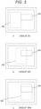
- Fig. 3 is views illustrating a definition of an overlap amount between the laser driver 200 and the semiconductor laser 300 according to the embodiment of the present technology.
- the semiconductor laser 300 and the laser driver 200 are arranged to overlap when viewed from the upper surface. Meanwhile, it is desirable to provide the thermal via 102 in a lower surface of the semiconductor laser 300, and a region therefor needs to be secured. Therefore, to clarify the positional relationship between the laser driver 200 and the semiconductor laser 300, the overlap amount between the laser driver 200 and the semiconductor laser 300 is defined as follows.
- no overlapping region is present between the semiconductor laser 300 and the laser driver 200 when viewed from the upper surface.
- the overlap amount in this case is defined as 0%.
- the entire semiconductor laser 300 overlaps with the laser driver 200 when viewed from the upper surface.
- the overlap amount in this case is defined as 100%.
- a half region of the semiconductor laser 300 overlaps with the laser driver 200 when viewed from the upper surface.
- the overlap amount in this case is defined as 50%.
- the overlap amount is desirably larger than 0% in order to provide a region for the above-described connection via 101.
- the overlap amount is desirably 50% or less. Therefore, by setting the overlap amount to be larger than 0% and to be 50% or less, the wiring inductance can be made small and favorable heat dissipation characteristics can be obtained.
- the wiring inductance is the problem. All conductors have an inductive component, and even an inductance of a very short lead may be detrimental in a high-frequency region of such a ToF system. That is, at high-frequency operation, a drive waveform for driving the semiconductor laser 300 from the laser driver 200 may be distorted due to the influence of the wiring inductance, and the operation may become unstable.
- the inductance IDC [ ⁇ H] of a strip line (substrate wiring pattern) having a length L [mm], a width W [mm], and a thickness H [mm] is expressed by the following expression in free space.
- IDC 0.0002 L ⁇ ln 2 L / W + H + 0.2235 W + H / L + 0.5
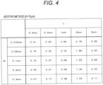
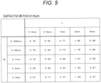
- Figs. 4 and 5 are tables illustrating trial calculations of the wiring inductance [nH] between the laser driver built in the printed wiring board and the semiconductor laser electrically connected to an upper portion of the printed wiring board.
- Fig. 4 is a diagram illustrating numerical value examples of the wiring inductance with respect to the wiring length L and the wiring width W in a case of forming a wiring pattern by an additive method.
- the additive method is a method of forming a pattern by depositing copper only on a necessary portion of an insulating resin surface.
- Fig. 5 is a diagram illustrating numerical value examples of the wiring inductance with respect to the wiring length L and the wiring width W in a case of forming a wiring pattern by a subtractive method.
- the subtractive method is a method of forming a pattern by etching an unnecessary portion of a copper clad laminate.
- the wiring inductance is desirably 0.5 nH or less, and more favorably 0.3 nH or less, assuming that the semiconductor laser drive device is driven at several hundreds of megahertz. Therefore, considering the above-described trial calculation results, it is considered that the wiring length between the semiconductor laser 300 and the laser driver 200 is desirably 0.5 millimeters or less, and more favorably 0.3 millimeters or less.
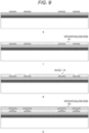
- Figs. 6 and 7 are views illustrating an example of steps of processing a copper land and a copper wiring layer (redistribution layer (RDL)) in the process of manufacturing the laser driver 200 according to the embodiment of the present technology.
- RDL distributed layer
- an I/O pad 210 formed using, for example, aluminum is formed on a semiconductor wafer. Then, a protective insulating layer 220 such as SiN is formed on a surface, and a region of the I/O pad 210 is opened.
- a surface protective film 230 formed using polyimide (PI) or polybenzoxazole (PBO) is formed, and a region of the I/O pad 210 is opened.
- titanium tungsten (TiW) having a thickness of several tens to 100 nm and copper (Cu) having a thickness of 100 to 1000 nm are continuously sputtered to form an adhesion layer and a seed layer 240.
- adhesion layer high melting point metal such as chromium (Cr), nickel (Ni), titanium (Ti), titanium copper (TiCu), or platinum (Pt) or its alloy may be applied, other than titanium tungsten (TiW).
- nickel (Ni), silver (Ag), gold (Au), or its alloy may be applied, other than copper (Cu).
- a photoresist 250 is patterned in order to form a copper land and a copper wiring layer for electrical connection.
- the photoresist 250 is formed by steps of surface cleaning, resist coating, drying, exposure, and development.
- a copper land and copper wiring layer (RDL) 260 for electrical connection is formed on the adhesion layer and the seed layer 240 by a plating method.
- the plating method for example, an electrolytic copper plating method, an electrolytic nickel plating method, or other method can be used.
- the diameter of the copper land is desirably about 50 to 100 micrometers
- the thickness of the copper wiring layer is desirably about 3 to 10 micrometers
- the minimum width of the copper wiring layer is desirably about 10 micrometers.
- the photoresist 250 is removed, and the copper land and copper wiring layer (RDL) 260 of the semiconductor chip is masked and dry-etched.
- RDL copper land and copper wiring layer
- the dry etching ion milling for emitting an argon ion beam can be used, for example.
- the adhesion layer and the seed layer 240 in an unnecessary region can be selectively removed, and the copper land and the copper wiring layer are separated.
- the unnecessary region can be removed by wet etching with aqua regia, or an aqueous solution of ceric ammonium nitrate, potassium hydroxide, or the like but dry etching is desirable considering side etching and thickness reduction of a metal layer constituting the copper land and the copper wiring layer.
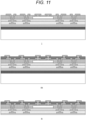
- Figs. 8 to 12 are views illustrating an example of steps of manufacturing the substrate 100 according to the embodiment of the present technology.
- a peelable copper foil 130 having a two-layer structure of an ultra-thin copper foil 132 and a carrier copper foil 131 is thermally bonded by roll laminating or laminating press on one side of a support plate 110 via an adhesive resin layer 120.
- a substrate formed using an inorganic material, a metal material, a resin material, or the like can be used as the support plate 110.
- silicon (Si) glass, ceramic, copper, a copper alloy, aluminum, an aluminum alloy, stainless steel, a polyimide resin, or an epoxy resin can be used.
- peelable copper foil 130 a copper foil obtained by vacuum-bonding the carrier copper foil 131 having the thickness of 18 to 35 micrometers to the ultra-thin copper foil 132 having the thickness of 2 to 5 micrometers each other.
- peelable copper foil 130 3FD-P3/35 (manufactured by Furukawa Circuit Foil Co., Ltd.), MT-18S5DH (manufactured by Mitsui Mining & Smelting Co., Ltd.), or the like can be used, for example.
- an organic resin such as an epoxy resin, a polyimide resin, a PPE resin, a phenol resin, a PTFE resin, a silicon resin, a polybutadiene resin, a polyester resin, a melamine resin, a urea resin, a PPS resin, or a PPO resin, which contains glass fiber reinforcing material, can be used.
- an organic resin such as an epoxy resin, a polyimide resin, a PPE resin, a phenol resin, a PTFE resin, a silicon resin, a polybutadiene resin, a polyester resin, a melamine resin, a urea resin, a PPS resin, or a PPO resin, which contains glass fiber reinforcing material
- aramid non-woven fabric, aramid fiber, polyester fiber, or the like can be used other than glass fiber.
- a plating base conductive layer (not illustrated) having the thickness of 0.5 to 3 micrometers is formed on the surface of the ultra-thin copper foil 132 of the peelable copper foil 130 by electroless copper plating treatment.
- the electroless copper plating treatment is to form a base conductive layer of electrolytic copper plating for forming a wiring pattern next.
- the electroless copper plating treatment may be omitted, and an electrode for electrolytic copper plating may be directly brought in contact with the peelable copper foil 130, and electrolytic copper plating treatment may be directly applied on the peelable copper foil 130 to form a wiring pattern.
- a photosensitive resist is attached to the surface of the support plate by roll laminating to form a resist pattern for the wiring pattern (solder resist 140).
- a photosensitive resist for example, a dry film plating resist can be used.
- a wiring pattern 150 having the thickness of about 15 micrometers is formed by the electrolytic copper plating treatment.
- the plating resist is peeled off.
- the surface of the wiring pattern is roughened to improve adhesiveness between the interlayer insulating resin and the wiring pattern.
- the roughening treatment can be performed by blackening treatment by oxidation-reduction treatment or hydrogen peroxide-sulfuric acid-based soft etching treatment.
- an interlayer insulating resin 161 is thermally bonded by roll laminating or laminating press on the wiring pattern.
- an epoxy resin having the thickness of 45 micrometers is rolled and laminated.
- copper foils having an arbitrary thickness are laminated and thermally compressed by laminating press.
- an organic resin such as an epoxy resin, a polyimide resin, a PPE resin, a phenol resin, a PTFE resin, a silicon resin, a polybutadiene resin, a polyester resin, a melamine resin, a urea resin, a PPS resin, or a PPO resin can be used.
- each of these resins can be used alone, or a combination of resins by mixing a plurality of the resins or preparing a compound can also be used, for example.
- an interlayer insulating resin obtained by including an inorganic filler in these materials or mixing a glass fiber reinforcing material can also be used.
- a via hole for interlayer electrical connection is formed by a laser method or a photoetching method.
- the via hole is formed by the laser method.
- laser light an ultraviolet laser such as a harmonic YAG laser or an excimer laser, or an infrared laser such as a carbon dioxide gas laser can be used. Note that, in the case of forming the via hole using the laser light, a thin resin film may remain on a bottom of the via hole, so desmear treatment is performed.
- the resin In the desmear treatment, the resin is swollen with a strong alkali, and the resin is decomposed and removed by using an oxidizing agent such as a chromic acid or a permanganate aqueous solution. Furthermore, the resin may be removed by plasma treatment or sandblast treatment with an abrasive.
- a via hole 170 is formed by a photoetching method. That is, the via hole 170 is formed by exposing the interlayer insulating resin 161 using ultraviolet rays through a mask and then performing development.
- electroless plating treatment is performed on a wall surface of the via hole 170 and a surface of the interlayer insulating resin 161.
- a photosensitive resist is attached by roll laminating to the surface of the interlayer insulating resin 161 to which the electroless plating treatment has been applied.
- the photosensitive resist for example, a dry film photosensitive plating resist film can be used. This photosensitive plating resist film is exposed and then developed to form a plating resist pattern in which the via hole 170 and the wiring pattern are opened.
- the electrolytic copper plating treatment with the thickness of 15 micrometers is applied to the opening in the plating resist pattern.
- the plating resist is peeled off, and the electroless plating remaining on the interlayer insulating resin is removed by hydrogen peroxide-sulfuric acid-based flash etching or the like, whereby the via hole 170 filled with copper plating and the wiring pattern, as illustrated in h in Fig. 9 , are formed.
- a similar step of roughening the wiring pattern and a similar step of forming an interlayer insulating resin 162 are repeatedly performed.
- the laser driver 200 obtained by attaching the copper land and the copper wiring layer thinned to the thickness of about 30 to 50 micrometers to a die attach film (DAF) 290 are mounted in a face-up state.
- DAF die attach film
- an interlayer insulating resin 163 is thermally bonded by roll laminating or laminating press.
- via hole treatment, desmear treatment, roughening treatment, electroless plating treatment, and electrolytic plating treatment similar to the above are performed. Note that processing for a shallow via hole 171 in the copper land of the laser driver 200, processing for a deep via hole 172 in one lower level, the desmear treatment, and the roughening treatment are simultaneously performed.
- the shallow via hole 171 is a filled via filled with copper plating.
- the size and depth of each via are about 20 to 30 micrometers.
- the size of the land is about 60 to 80 micrometers in diameter.
- the deep via hole 172 is a so-called conformal via having copper plating applied only to an outside of the via.
- the size and depth of each via are about 80 to 150 micrometers.
- the size of the land is about 150 to 200 micrometers in diameter.
- the deep via hole 172 is desirably arranged at a distance of about 100 micrometers from an outer shape of the laser driver 200 via an insulating resin.
- an interlayer insulating resin similar to the above is thermally bonded by roll laminating or laminating press. At this time, the inside of the conformal via is filled with the interlayer insulating resin. Next, via hole treatment, desmear treatment, roughening treatment, electroless plating treatment, and electrolytic plating treatment similar to the above are performed.
- the support plate 110 is separated by being peeled from an interface between the carrier copper foil 131 of the peelable copper foil 130 and the ultra-thin copper foil 132.
- the ultra-thin copper foil 132 and the plating base conductive layer are removed using sulfuric acid-hydrogen peroxide-based soft etching, whereby a substrate having components built-in with an exposed wiring pattern can be obtained.
- a solder resist 180 having a pattern having an opening in a land portion of the wiring pattern is printed on the exposed wiring pattern.
- the solder resist 180 can be formed by a roll coater using a film type.
- electroless Ni plating is formed on the land portion of the opening of the solder resist 180 in the thickness of 3 micrometers or more, and electroless Au plating is formed on the electroless Ni plating in the thickness of 0.03 micrometers or more.
- the electroless Au plating may be formed in the thickness of 1 micrometer or more.
- the electroless Au plating may be precoated with a solder.
- electrolytic Ni plating may be formed in the opening of the solder resist 180 in the thickness of 3 micrometers or more, and electrolytic Au plating may be formed on the electrolytic Ni plating in the thickness of 0.5 micrometers or more.
- an organic rustproof film may be formed in the opening of the solder resist 180, other than metal plating.
- a cream solder may be applied and printed to mount a solder ball grid array (BGA) as a connection terminal on the land for external connection.
- BGA solder ball grid array
- a copper core ball, a copper pillar bump, a land grid array (LGA), or the like may be used as the connection terminal.
- the semiconductor laser 300, the photodiode 400, and the passive component 500 are mounted and the side wall 600 and the diffusion plate 700 are attached to the surface of the substrate 100 manufactured as described above, as illustrated in q in Fig. 12 .
- an outer shape is processed by a dicer or the like to be separated into individual pieces.
- a copper clad laminate (CCL) can be used instead of the peelable copper foil 130 and the support plate 110.
- CCL copper clad laminate
- a method of forming a cavity in the substrate and mounting the components may be used as the manufacturing method incorporating the components into the substrate.
- the electrical connection between the semiconductor laser 300 and the laser driver 200 is performed via the connection via 101, whereby the wiring inductance can be reduced.
- the wiring length between the electrical connection between the semiconductor laser 300 and the laser driver 200 is set to 0.5 millimeters or less, whereby the wiring inductance can be set to 0.5 nanohenries or less.
- the overlap amount between the semiconductor laser 300 and the laser driver 200 is set to 50% or less, whereby a certain number of thermal vias 102 can be arranged immediately below the semiconductor laser 300, and favorable heat dissipation characteristics can be obtained.
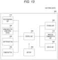
- Fig. 13 is a diagram illustrating a system configuration example of an electronic device 800 as an application of the embodiment of the present technology.
- the electronic device 800 is a mobile terminal equipped with the semiconductor laser drive device 10 according to the above-described embodiment.
- the electronic device 800 includes an imaging unit 810, a semiconductor laser drive device 820, a shutter button 830, a power button 840, a control unit 850, a storage unit 860, a wireless communication unit 870, a display unit 880, and a battery 890.
- the imaging unit 810 is an image sensor that captures an image of an object.
- the semiconductor laser drive device 820 is the semiconductor laser drive device 10 according to the above-described embodiment.
- the shutter button 830 is a button for giving an instruction on imaging timing of the imaging unit 810 from an outside of the electronic device 800.
- the power button 840 is a button for giving an instruction on on/off of power of the electronic device 800 from the outside of the electronic device 800.
- the control unit 850 is a processing unit that controls the entire electronic device 800.
- the storage unit 860 is a memory that stores data and programs necessary for operation of the electronic device 800.
- the wireless communication unit 870 performs wireless communication with the outside of the electronic device 800.
- the display unit 880 is a display that displays images and the like.
- the battery 890 is a power supply source that supplies power to each unit of the electronic device 800.
- a specific phase (for example, rising timing) of a light emission control signal for controlling the imaging unit 810 and the semiconductor laser drive device 820 is set to 0 degrees, and a light receiving amount from 0 degrees to 180 degrees is detected as Q1, and the light receiving amount from 180 degrees to 360 degrees is detected as Q2. Furthermore, the imaging unit 810 detects the light receiving amount from 90 degrees to 270 degrees as Q3, and detects the light receiving amount from 270 degrees to 90 degrees as Q4.
- the control unit 850 calculates a distance d to the object from these light receiving amounts Q1 to Q4 by the following expression, and displays the distance d on the display unit 880.
- d c / 4 ⁇ f ⁇ arctan Q 3 ⁇ Q 4 / Q 1 ⁇ Q 2
- the unit of the distance d is, for example, meter (m).
- c represents a light speed, and the unit of the light speed is, for example, meter per second (m/s).
- arctan is an inverse function of a tangent function.
- the value of "(Q3 - Q4)/(Q1 - Q2)" indicates a phase difference between irradiation light and reflected light.
- ⁇ represents pi.
- f represents a frequency of the irradiation light, and its unit is, for example, megahertz (MHz) .
- Fig. 14 is a view illustrating an external configuration example of the electronic device 800 as an application of the embodiment of the present technology.
- the electronic device 800 is housed in a housing 801 and includes the power button 840 on a side surface and the display unit 880 and the shutter button 830 on a surface. Furthermore, optical regions of the imaging unit 810 and the semiconductor laser drive device 820 are provided on a back surface.
- the display unit 880 can display not only a normal captured image 881 but also a depth image 882 according to a distance measurement result using ToF.
- a mobile terminal such as a smartphone has been illustrated as the electronic device 800, but the electronic device 800 is not limited to the example and may be a digital camera, a game machine, a wearable device, or the like, for example.
Landscapes
- Physics & Mathematics (AREA)
- General Physics & Mathematics (AREA)
- Electromagnetism (AREA)
- Condensed Matter Physics & Semiconductors (AREA)
- Optics & Photonics (AREA)
- Engineering & Computer Science (AREA)
- Manufacturing & Machinery (AREA)
- Microelectronics & Electronic Packaging (AREA)
- Computer Networks & Wireless Communication (AREA)
- Radar, Positioning & Navigation (AREA)
- Remote Sensing (AREA)
- Semiconductor Lasers (AREA)
- Photo Coupler, Interrupter, Optical-To-Optical Conversion Devices (AREA)
- Production Of Multi-Layered Print Wiring Board (AREA)
- Optical Radar Systems And Details Thereof (AREA)
Claims (9)
- Dispositif de pilotage de laser à semi-conducteur (10) comprenant :un substrat (100) ayant un pilote laser (200) intégré ;un laser à semi-conducteur (300) monté sur une surface du substrat (100) ; etun câblage de connexion (101) configuré pour connecter électriquement de manière directe le pilote laser (200) et le laser à semi-conducteur (300) par une inductance de câblage inférieure ou égale à 0,5 nanohenry, dans lequelle câblage de connexion (101) est fourni par l'intermédiaire d'un passage de connexion (101) fourni dans le substrat (100),le câblage de connexion (101) a une longueur de 0,5 millimètre ou moins, la longueur de câblage de connexion étant définie par la distance du câblage de connexion (101) qui est la distance du passage de connexion (101) entre le pilote laser (200) et le laser à semi-conducteur (300), etune partie du laser à semi-conducteur (300) est agencée par-dessus le passage de connexion (101) et par-dessus le pilote laser (200).
- Dispositif de pilotage de laser à semi-conducteur (10) selon la revendication 1, dans lequel
une partie du laser à semi-conducteur (300), la partie ayant une aire de 50 % ou moins du laser à semi-conducteur (300), est agencée par-dessus le pilote laser (200). - Dispositif de pilotage de laser à semi-conducteur (10) selon la revendication 1, dans lequel
le substrat (100) comporte un passage thermique (102) au niveau d'une position où le laser à semi-conducteur (300) est monté. - Dispositif de pilotage de laser à semi-conducteur (10) selon la revendication 1, comprenant en outre :une paroi externe (600) entourant une région comportant le laser à semi-conducteur (300) dans la surface précitée du substrat (100) ; etune plaque de diffusion (700) couvrant une région supérieure de la région entourée par la paroi externe (600).
- Dispositif de pilotage de laser à semi-conducteur (10) selon la revendication 1, comprenant en outre :
une photodiode (400) montée sur la surface précitée du substrat (100) et configurée pour surveiller une intensité de lumière d'une lumière laser émise à partir du laser à semi-conducteur (300). - Dispositif de pilotage de laser à semi-conducteur (10) selon la revendication 1, comprenant en outre :
une borne de connexion à connecter à un extérieur sur une surface opposée de la surface précitée du substrat (100). - Dispositif de pilotage de laser à semi-conducteur (10) selon la revendication 6, dans lequel
la borne de connexion est formée par au moins l'un parmi une bille de soudure, une bille à noyau de cuivre, un bossage surélevé de cuivre ou une grille matricielle à billes. - Dispositif électronique (800) comprenant le dispositif de pilotage de laser à semi-conducteur selon la revendication 1.
- Procédé de fabrication d'un dispositif de pilotage de laser à semi-conducteur (10), le procédé comprenant :une procédure de formation d'un pilote laser (200) sur une surface supérieure d'une plaque de support (110) ;une procédure de formation d'un câblage de connexion du pilote laser pour former un substrat (100) ayant le pilote laser intégré ; etune procédure de montage d'un laser à semi-conducteur (300) sur une surface du substrat (100) et la formation d'un câblage de connexion (101) qui connecte électriquement de manière directe le pilote laser (200) et le laser à semi-conducteur (300) par une inductance de câblage de 0,5 nanohenry ou moins par l'intermédiaire du câblage de connexion (101), dans lequelle câblage de connexion (101) est fourni par l'intermédiaire d'un passage de connexion (101) fourni dans le substrat (100),le câblage de connexion (101) a une longueur de 0,5 millimètre ou moins, la longueur de câblage de connexion étant définie par la distance du câblage de connexion (101) qui est la distance du passage de connexion (101) entre le pilote laser (200) et le laser à semi-conducteur (300), etune partie du laser à semi-conducteur (300) est agencée par-dessus le passage de connexion (101) et par-dessus le pilote laser (200).
Applications Claiming Priority (2)
| Application Number | Priority Date | Filing Date | Title |
|---|---|---|---|
| JP2018080518 | 2018-04-19 | ||
| PCT/JP2019/009591 WO2019202874A1 (fr) | 2018-04-19 | 2019-03-11 | Dispositif de pilotage de laser à semi-conducteur et son procédé de fabrication |
Publications (3)
| Publication Number | Publication Date |
|---|---|
| EP3783759A1 EP3783759A1 (fr) | 2021-02-24 |
| EP3783759A4 EP3783759A4 (fr) | 2021-06-30 |
| EP3783759B1 true EP3783759B1 (fr) | 2024-05-01 |
Family
ID=68240038
Family Applications (1)
| Application Number | Title | Priority Date | Filing Date |
|---|---|---|---|
| EP19787571.9A Active EP3783759B1 (fr) | 2018-04-19 | 2019-03-11 | Dispositif de pilotage de laser à semi-conducteur et son procédé de fabrication |
Country Status (6)
| Country | Link |
|---|---|
| US (2) | US11962123B2 (fr) |
| EP (1) | EP3783759B1 (fr) |
| JP (2) | JP7329502B2 (fr) |
| KR (2) | KR20240015727A (fr) |
| CN (2) | CN112005455B (fr) |
| WO (1) | WO2019202874A1 (fr) |
Families Citing this family (12)
| Publication number | Priority date | Publication date | Assignee | Title |
|---|---|---|---|---|
| EP3783759B1 (fr) | 2018-04-19 | 2024-05-01 | Sony Semiconductor Solutions Corporation | Dispositif de pilotage de laser à semi-conducteur et son procédé de fabrication |
| CN114175425A (zh) * | 2019-07-30 | 2022-03-11 | 索尼半导体解决方案公司 | 半导体激光驱动装置、电子设备和半导体激光驱动装置的制造方法 |
| JP7356287B2 (ja) * | 2019-08-06 | 2023-10-04 | ソニーセミコンダクタソリューションズ株式会社 | 半導体レーザ駆動装置、および、電子機器 |
| US12327980B2 (en) * | 2019-08-20 | 2025-06-10 | Sony Semiconductor Solutions Corporation | Semiconductor laser driving apparatus, electronic equipment, and manufacturing method of semiconductor laser driving apparatus |
| JP7411350B2 (ja) * | 2019-08-20 | 2024-01-11 | ソニーセミコンダクタソリューションズ株式会社 | 測距装置、電子機器、および、測距装置の製造方法 |
| US12261411B2 (en) | 2019-08-30 | 2025-03-25 | Sony Semiconductor Solutions Corporation | Semiconductor laser driving apparatus, electronic equipment, and manufacturing method of semiconductor laser driving apparatus |
| EP4071945B1 (fr) * | 2020-01-13 | 2025-03-26 | Nuvoton Technology Corporation Japan | Dispositif à semi-conducteurs |
| JP7521203B2 (ja) | 2020-02-26 | 2024-07-24 | 富士フイルムビジネスイノベーション株式会社 | 発光装置、光学装置及び計測装置 |
| WO2021181862A1 (fr) * | 2020-03-11 | 2021-09-16 | ソニーセミコンダクタソリューションズ株式会社 | Dispositif de commande de laser à semi-conducteur |
| JP7521216B2 (ja) * | 2020-03-24 | 2024-07-24 | 富士フイルムビジネスイノベーション株式会社 | 発光装置、光学装置、計測装置及び情報処理装置 |
| WO2021235143A1 (fr) * | 2020-05-21 | 2021-11-25 | ソニーセミコンダクタソリューションズ株式会社 | Dispositif électronique |
| CN116420092A (zh) * | 2020-11-06 | 2023-07-11 | 索尼半导体解决方案公司 | 半导体激光驱动装置、包括半导体激光驱动装置的lidar以及包括半导体激光驱动装置的车辆 |
Family Cites Families (34)
| Publication number | Priority date | Publication date | Assignee | Title |
|---|---|---|---|---|
| JPH09307174A (ja) * | 1996-05-15 | 1997-11-28 | Ricoh Co Ltd | 分散光源装置 |
| JPH1191165A (ja) | 1997-09-25 | 1999-04-06 | Canon Inc | 画像形成装置 |
| JPH11238907A (ja) * | 1998-02-20 | 1999-08-31 | Advantest Corp | 広帯域サンプラモジュール |
| JP2001339077A (ja) | 2000-03-24 | 2001-12-07 | Matsushita Electric Ind Co Ltd | 半導体素子実装装置および光通信装置 |
| JP2002232062A (ja) * | 2001-02-02 | 2002-08-16 | Ricoh Co Ltd | 光電子集積素子 |
| US6759740B2 (en) * | 2001-03-30 | 2004-07-06 | Kyocera Corporation | Composite ceramic board, method of producing the same, optical/electronic-mounted circuit substrate using said board, and mounted board equipped with said circuit substrate |
| JP3847103B2 (ja) | 2001-05-30 | 2006-11-15 | 京セラ株式会社 | 光電子実装回路基板及び実装基板 |
| JP4004333B2 (ja) | 2001-06-05 | 2007-11-07 | 松下電器産業株式会社 | 半導体モジュール |
| JP2003249712A (ja) | 2001-12-19 | 2003-09-05 | Matsushita Electric Ind Co Ltd | 光モジュール |
| JP2004031456A (ja) | 2002-06-21 | 2004-01-29 | Fujitsu Ltd | 光インタコネクション装置及びインタコネクションモジュール |
| US7061949B1 (en) * | 2002-08-16 | 2006-06-13 | Jds Uniphase Corporation | Methods, apparatus, and systems with semiconductor laser packaging for high modulation bandwidth |
| JP2004128342A (ja) * | 2002-10-04 | 2004-04-22 | Sharp Corp | レーザドライバ内蔵半導体レーザ装置およびそれを備えた電子機器 |
| JP2004241505A (ja) | 2003-02-04 | 2004-08-26 | Ntt Electornics Corp | E/o変換回路 |
| KR100594063B1 (ko) * | 2004-01-15 | 2006-06-30 | 삼성전자주식회사 | 반도체 광소자와 그를 이용한 반도체 광패키지 |
| JP5065062B2 (ja) | 2008-01-16 | 2012-10-31 | 古河電気工業株式会社 | 光モジュール |
| JP2011060875A (ja) * | 2009-09-08 | 2011-03-24 | Panasonic Corp | 電子部品内蔵基板及びその製造方法とこれを用いた半導体装置 |
| KR101711961B1 (ko) | 2010-09-10 | 2017-03-03 | 삼성전자주식회사 | 발광 디바이스 |
| US10234545B2 (en) | 2010-12-01 | 2019-03-19 | Microsoft Technology Licensing, Llc | Light source module |
| US8487407B2 (en) * | 2011-10-13 | 2013-07-16 | Infineon Technologies Ag | Low impedance gate control method and apparatus |
| EP2600168A1 (fr) * | 2011-12-01 | 2013-06-05 | Leica Geosystems AG | Appareil de mesure de distance |
| US8675706B2 (en) | 2011-12-24 | 2014-03-18 | Princeton Optronics Inc. | Optical illuminator |
| US20130163627A1 (en) | 2011-12-24 | 2013-06-27 | Princeton Optronics | Laser Illuminator System |
| US8882310B2 (en) * | 2012-12-10 | 2014-11-11 | Microsoft Corporation | Laser die light source module with low inductance |
| DE102013114547B4 (de) * | 2013-01-18 | 2020-01-16 | Schott Ag | TO-Gehäuse |
| US8958448B2 (en) | 2013-02-04 | 2015-02-17 | Microsoft Corporation | Thermal management in laser diode device |
| WO2015146377A1 (fr) * | 2014-03-24 | 2015-10-01 | シチズンホールディングス株式会社 | Élément de montage pour fibre optique, module optique, et procédé de fabrication de module optique |
| CN106104344B (zh) * | 2014-03-24 | 2017-11-10 | 西铁城时计株式会社 | 光纤的安装零件、光模块以及制造方法 |
| US9577406B2 (en) * | 2014-06-27 | 2017-02-21 | Microsoft Technology Licensing, Llc | Edge-emitting laser diode package comprising heat spreader |
| KR102667851B1 (ko) | 2016-02-22 | 2024-05-23 | 삼성디스플레이 주식회사 | 디스플레이 장치 |
| JP6799985B2 (ja) * | 2016-09-28 | 2020-12-16 | 株式会社トプコン | 測距装置 |
| DE102016125430A1 (de) | 2016-12-22 | 2018-06-28 | Osram Opto Semiconductors Gmbh | Oberflächenmontierbarer Halbleiterlaser, Anordnung mit einem solchen Halbleiterlaser und Betriebsverfahren hierfür |
| US20180278011A1 (en) * | 2017-03-23 | 2018-09-27 | Infineon Technologies Ag | Laser diode module |
| DE102017108050B4 (de) * | 2017-04-13 | 2022-01-13 | OSRAM Opto Semiconductors Gesellschaft mit beschränkter Haftung | Halbleiterstrahlungsquelle |
| EP3783759B1 (fr) | 2018-04-19 | 2024-05-01 | Sony Semiconductor Solutions Corporation | Dispositif de pilotage de laser à semi-conducteur et son procédé de fabrication |
-
2019
- 2019-03-11 EP EP19787571.9A patent/EP3783759B1/fr active Active
- 2019-03-11 CN CN201980025330.7A patent/CN112005455B/zh active Active
- 2019-03-11 US US17/046,836 patent/US11962123B2/en active Active
- 2019-03-11 CN CN202410618280.6A patent/CN118472790A/zh active Pending
- 2019-03-11 KR KR1020247002369A patent/KR20240015727A/ko active Pending
- 2019-03-11 KR KR1020207028974A patent/KR102629637B1/ko active Active
- 2019-03-11 JP JP2020514012A patent/JP7329502B2/ja active Active
- 2019-03-11 WO PCT/JP2019/009591 patent/WO2019202874A1/fr not_active Ceased
-
2023
- 2023-08-07 JP JP2023128389A patent/JP7499391B2/ja active Active
-
2024
- 2024-01-16 US US18/414,180 patent/US12249806B2/en active Active
Also Published As
| Publication number | Publication date |
|---|---|
| WO2019202874A1 (fr) | 2019-10-24 |
| JPWO2019202874A1 (ja) | 2021-05-13 |
| KR20240015727A (ko) | 2024-02-05 |
| US20240154385A1 (en) | 2024-05-09 |
| JP2023145742A (ja) | 2023-10-11 |
| JP7499391B2 (ja) | 2024-06-13 |
| JP7329502B2 (ja) | 2023-08-18 |
| CN118472790A (zh) | 2024-08-09 |
| US12249806B2 (en) | 2025-03-11 |
| KR102629637B1 (ko) | 2024-01-30 |
| CN112005455A (zh) | 2020-11-27 |
| US20210143607A1 (en) | 2021-05-13 |
| EP3783759A4 (fr) | 2021-06-30 |
| US11962123B2 (en) | 2024-04-16 |
| KR20220060447A (ko) | 2022-05-11 |
| EP3783759A1 (fr) | 2021-02-24 |
| CN112005455B (zh) | 2024-06-04 |
Similar Documents
| Publication | Publication Date | Title |
|---|---|---|
| EP3783759B1 (fr) | Dispositif de pilotage de laser à semi-conducteur et son procédé de fabrication | |
| US12376271B2 (en) | Semiconductor laser driving apparatus, electronic equipment, and manufacturing method of semiconductor laser driving apparatus | |
| US12261411B2 (en) | Semiconductor laser driving apparatus, electronic equipment, and manufacturing method of semiconductor laser driving apparatus | |
| EP4019895A1 (fr) | Dispositif de commande de laser à semi-conducteur, appareil électronique et procédé de fabrication d'un dispositif de commande de laser à semi-conducteur | |
| KR102918499B1 (ko) | 반도체 레이저 구동 장치, 전자 기기, 및 반도체 레이저 구동 장치의 제조 방법 | |
| US20220302674A1 (en) | Semiconductor laser driving apparatus, electronic equipment, and manufacturing method of semiconductor laser driving apparatus | |
| EP4033620A1 (fr) | Dispositif d'attaque de laser semi-conducteur, appareil électronique, et procédé destiné à fabriquer un dispositif d'attaque de laser semi-conducteur | |
| US12567718B2 (en) | Semiconductor laser driving apparatus, electronic equipment, and manufacturing method of semiconductor laser driving apparatus | |
| US12283792B2 (en) | Light emitting device, and electronic apparatus | |
| EP4007090A1 (fr) | Dispositif d'attaque de laser à semi-conducteur, appareil électronique et procédé de fabrication de dispositif d'attaque de laser à semi-conducteur |
Legal Events
| Date | Code | Title | Description |
|---|---|---|---|
| STAA | Information on the status of an ep patent application or granted ep patent |
Free format text: STATUS: THE INTERNATIONAL PUBLICATION HAS BEEN MADE |
|
| PUAI | Public reference made under article 153(3) epc to a published international application that has entered the european phase |
Free format text: ORIGINAL CODE: 0009012 |
|
| STAA | Information on the status of an ep patent application or granted ep patent |
Free format text: STATUS: REQUEST FOR EXAMINATION WAS MADE |
|
| 17P | Request for examination filed |
Effective date: 20201012 |
|
| AK | Designated contracting states |
Kind code of ref document: A1 Designated state(s): AL AT BE BG CH CY CZ DE DK EE ES FI FR GB GR HR HU IE IS IT LI LT LU LV MC MK MT NL NO PL PT RO RS SE SI SK SM TR |
|
| AX | Request for extension of the european patent |
Extension state: BA ME |
|
| A4 | Supplementary search report drawn up and despatched |
Effective date: 20210601 |
|
| RIC1 | Information provided on ipc code assigned before grant |
Ipc: H01S 5/02345 20210101AFI20210526BHEP Ipc: H01S 5/02325 20210101ALI20210526BHEP Ipc: G01S 7/484 20060101ALI20210526BHEP Ipc: G01S 17/894 20200101ALI20210526BHEP Ipc: H05K 3/46 20060101ALI20210526BHEP Ipc: H01L 23/00 20060101ALI20210526BHEP Ipc: H01S 5/024 20060101ALN20210526BHEP Ipc: H01S 5/062 20060101ALN20210526BHEP Ipc: H01S 5/0683 20060101ALN20210526BHEP |
|
| DAV | Request for validation of the european patent (deleted) | ||
| DAX | Request for extension of the european patent (deleted) | ||
| REG | Reference to a national code |
Ref country code: DE Ref legal event code: R079 Free format text: PREVIOUS MAIN CLASS: H01S0005022000 Ipc: H01S0005023450 Ref document number: 602019051500 Country of ref document: DE |
|
| RIC1 | Information provided on ipc code assigned before grant |
Ipc: H01S 5/0239 20210101ALN20231019BHEP Ipc: H01S 5/02257 20210101ALN20231019BHEP Ipc: H01S 5/0683 20060101ALN20231019BHEP Ipc: H01S 5/062 20060101ALN20231019BHEP Ipc: H01S 5/024 20060101ALN20231019BHEP Ipc: H01L 23/00 20060101ALI20231019BHEP Ipc: H05K 3/46 20060101ALI20231019BHEP Ipc: G01S 17/894 20200101ALI20231019BHEP Ipc: G01S 7/484 20060101ALI20231019BHEP Ipc: H01S 5/02325 20210101ALI20231019BHEP Ipc: H01S 5/02345 20210101AFI20231019BHEP |
|
| GRAP | Despatch of communication of intention to grant a patent |
Free format text: ORIGINAL CODE: EPIDOSNIGR1 |
|
| STAA | Information on the status of an ep patent application or granted ep patent |
Free format text: STATUS: GRANT OF PATENT IS INTENDED |
|
| INTG | Intention to grant announced |
Effective date: 20231130 |
|
| RIC1 | Information provided on ipc code assigned before grant |
Ipc: H01S 5/0239 20210101ALN20231117BHEP Ipc: H01S 5/02257 20210101ALN20231117BHEP Ipc: H01S 5/0683 20060101ALN20231117BHEP Ipc: H01S 5/062 20060101ALN20231117BHEP Ipc: H01S 5/024 20060101ALN20231117BHEP Ipc: H01L 23/00 20060101ALI20231117BHEP Ipc: H05K 3/46 20060101ALI20231117BHEP Ipc: G01S 17/894 20200101ALI20231117BHEP Ipc: G01S 7/484 20060101ALI20231117BHEP Ipc: H01S 5/02325 20210101ALI20231117BHEP Ipc: H01S 5/02345 20210101AFI20231117BHEP |
|
| GRAS | Grant fee paid |
Free format text: ORIGINAL CODE: EPIDOSNIGR3 |
|
| GRAA | (expected) grant |
Free format text: ORIGINAL CODE: 0009210 |
|
| STAA | Information on the status of an ep patent application or granted ep patent |
Free format text: STATUS: THE PATENT HAS BEEN GRANTED |
|
| P01 | Opt-out of the competence of the unified patent court (upc) registered |
Effective date: 20240306 |
|
| AK | Designated contracting states |
Kind code of ref document: B1 Designated state(s): AL AT BE BG CH CY CZ DE DK EE ES FI FR GB GR HR HU IE IS IT LI LT LU LV MC MK MT NL NO PL PT RO RS SE SI SK SM TR |
|
| REG | Reference to a national code |
Ref country code: GB Ref legal event code: FG4D |
|
| REG | Reference to a national code |
Ref country code: CH Ref legal event code: EP |
|
| REG | Reference to a national code |
Ref country code: IE Ref legal event code: FG4D |
|
| REG | Reference to a national code |
Ref country code: DE Ref legal event code: R096 Ref document number: 602019051500 Country of ref document: DE |
|
| REG | Reference to a national code |
Ref country code: LT Ref legal event code: MG9D |
|
| REG | Reference to a national code |
Ref country code: NL Ref legal event code: MP Effective date: 20240501 |
|
| PG25 | Lapsed in a contracting state [announced via postgrant information from national office to epo] |
Ref country code: IS Free format text: LAPSE BECAUSE OF FAILURE TO SUBMIT A TRANSLATION OF THE DESCRIPTION OR TO PAY THE FEE WITHIN THE PRESCRIBED TIME-LIMIT Effective date: 20240901 |
|
| PG25 | Lapsed in a contracting state [announced via postgrant information from national office to epo] |
Ref country code: BG Free format text: LAPSE BECAUSE OF FAILURE TO SUBMIT A TRANSLATION OF THE DESCRIPTION OR TO PAY THE FEE WITHIN THE PRESCRIBED TIME-LIMIT Effective date: 20240501 |
|
| PG25 | Lapsed in a contracting state [announced via postgrant information from national office to epo] |
Ref country code: FI Free format text: LAPSE BECAUSE OF FAILURE TO SUBMIT A TRANSLATION OF THE DESCRIPTION OR TO PAY THE FEE WITHIN THE PRESCRIBED TIME-LIMIT Effective date: 20240501 Ref country code: HR Free format text: LAPSE BECAUSE OF FAILURE TO SUBMIT A TRANSLATION OF THE DESCRIPTION OR TO PAY THE FEE WITHIN THE PRESCRIBED TIME-LIMIT Effective date: 20240501 |
|
| PG25 | Lapsed in a contracting state [announced via postgrant information from national office to epo] |
Ref country code: GR Free format text: LAPSE BECAUSE OF FAILURE TO SUBMIT A TRANSLATION OF THE DESCRIPTION OR TO PAY THE FEE WITHIN THE PRESCRIBED TIME-LIMIT Effective date: 20240802 |
|
| PG25 | Lapsed in a contracting state [announced via postgrant information from national office to epo] |
Ref country code: PT Free format text: LAPSE BECAUSE OF FAILURE TO SUBMIT A TRANSLATION OF THE DESCRIPTION OR TO PAY THE FEE WITHIN THE PRESCRIBED TIME-LIMIT Effective date: 20240902 |
|
| REG | Reference to a national code |
Ref country code: AT Ref legal event code: MK05 Ref document number: 1683724 Country of ref document: AT Kind code of ref document: T Effective date: 20240501 |
|
| PG25 | Lapsed in a contracting state [announced via postgrant information from national office to epo] |
Ref country code: NL Free format text: LAPSE BECAUSE OF FAILURE TO SUBMIT A TRANSLATION OF THE DESCRIPTION OR TO PAY THE FEE WITHIN THE PRESCRIBED TIME-LIMIT Effective date: 20240501 |
|
| PG25 | Lapsed in a contracting state [announced via postgrant information from national office to epo] |
Ref country code: ES Free format text: LAPSE BECAUSE OF FAILURE TO SUBMIT A TRANSLATION OF THE DESCRIPTION OR TO PAY THE FEE WITHIN THE PRESCRIBED TIME-LIMIT Effective date: 20240501 |
|
| PG25 | Lapsed in a contracting state [announced via postgrant information from national office to epo] |
Ref country code: AT Free format text: LAPSE BECAUSE OF FAILURE TO SUBMIT A TRANSLATION OF THE DESCRIPTION OR TO PAY THE FEE WITHIN THE PRESCRIBED TIME-LIMIT Effective date: 20240501 |
|
| PG25 | Lapsed in a contracting state [announced via postgrant information from national office to epo] |
Ref country code: PL Free format text: LAPSE BECAUSE OF FAILURE TO SUBMIT A TRANSLATION OF THE DESCRIPTION OR TO PAY THE FEE WITHIN THE PRESCRIBED TIME-LIMIT Effective date: 20240501 |
|
| PG25 | Lapsed in a contracting state [announced via postgrant information from national office to epo] |
Ref country code: LV Free format text: LAPSE BECAUSE OF FAILURE TO SUBMIT A TRANSLATION OF THE DESCRIPTION OR TO PAY THE FEE WITHIN THE PRESCRIBED TIME-LIMIT Effective date: 20240501 |
|
| PG25 | Lapsed in a contracting state [announced via postgrant information from national office to epo] |
Ref country code: PT Free format text: LAPSE BECAUSE OF FAILURE TO SUBMIT A TRANSLATION OF THE DESCRIPTION OR TO PAY THE FEE WITHIN THE PRESCRIBED TIME-LIMIT Effective date: 20240902 Ref country code: PL Free format text: LAPSE BECAUSE OF FAILURE TO SUBMIT A TRANSLATION OF THE DESCRIPTION OR TO PAY THE FEE WITHIN THE PRESCRIBED TIME-LIMIT Effective date: 20240501 Ref country code: NO Free format text: LAPSE BECAUSE OF FAILURE TO SUBMIT A TRANSLATION OF THE DESCRIPTION OR TO PAY THE FEE WITHIN THE PRESCRIBED TIME-LIMIT Effective date: 20240801 Ref country code: NL Free format text: LAPSE BECAUSE OF FAILURE TO SUBMIT A TRANSLATION OF THE DESCRIPTION OR TO PAY THE FEE WITHIN THE PRESCRIBED TIME-LIMIT Effective date: 20240501 Ref country code: LV Free format text: LAPSE BECAUSE OF FAILURE TO SUBMIT A TRANSLATION OF THE DESCRIPTION OR TO PAY THE FEE WITHIN THE PRESCRIBED TIME-LIMIT Effective date: 20240501 Ref country code: IS Free format text: LAPSE BECAUSE OF FAILURE TO SUBMIT A TRANSLATION OF THE DESCRIPTION OR TO PAY THE FEE WITHIN THE PRESCRIBED TIME-LIMIT Effective date: 20240901 Ref country code: HR Free format text: LAPSE BECAUSE OF FAILURE TO SUBMIT A TRANSLATION OF THE DESCRIPTION OR TO PAY THE FEE WITHIN THE PRESCRIBED TIME-LIMIT Effective date: 20240501 Ref country code: GR Free format text: LAPSE BECAUSE OF FAILURE TO SUBMIT A TRANSLATION OF THE DESCRIPTION OR TO PAY THE FEE WITHIN THE PRESCRIBED TIME-LIMIT Effective date: 20240802 Ref country code: FI Free format text: LAPSE BECAUSE OF FAILURE TO SUBMIT A TRANSLATION OF THE DESCRIPTION OR TO PAY THE FEE WITHIN THE PRESCRIBED TIME-LIMIT Effective date: 20240501 Ref country code: ES Free format text: LAPSE BECAUSE OF FAILURE TO SUBMIT A TRANSLATION OF THE DESCRIPTION OR TO PAY THE FEE WITHIN THE PRESCRIBED TIME-LIMIT Effective date: 20240501 Ref country code: BG Free format text: LAPSE BECAUSE OF FAILURE TO SUBMIT A TRANSLATION OF THE DESCRIPTION OR TO PAY THE FEE WITHIN THE PRESCRIBED TIME-LIMIT Effective date: 20240501 Ref country code: AT Free format text: LAPSE BECAUSE OF FAILURE TO SUBMIT A TRANSLATION OF THE DESCRIPTION OR TO PAY THE FEE WITHIN THE PRESCRIBED TIME-LIMIT Effective date: 20240501 Ref country code: RS Free format text: LAPSE BECAUSE OF FAILURE TO SUBMIT A TRANSLATION OF THE DESCRIPTION OR TO PAY THE FEE WITHIN THE PRESCRIBED TIME-LIMIT Effective date: 20240801 |
|
| PG25 | Lapsed in a contracting state [announced via postgrant information from national office to epo] |
Ref country code: DK Free format text: LAPSE BECAUSE OF FAILURE TO SUBMIT A TRANSLATION OF THE DESCRIPTION OR TO PAY THE FEE WITHIN THE PRESCRIBED TIME-LIMIT Effective date: 20240501 |
|
| PG25 | Lapsed in a contracting state [announced via postgrant information from national office to epo] |
Ref country code: EE Free format text: LAPSE BECAUSE OF FAILURE TO SUBMIT A TRANSLATION OF THE DESCRIPTION OR TO PAY THE FEE WITHIN THE PRESCRIBED TIME-LIMIT Effective date: 20240501 |
|
| PG25 | Lapsed in a contracting state [announced via postgrant information from national office to epo] |
Ref country code: CZ Free format text: LAPSE BECAUSE OF FAILURE TO SUBMIT A TRANSLATION OF THE DESCRIPTION OR TO PAY THE FEE WITHIN THE PRESCRIBED TIME-LIMIT Effective date: 20240501 |
|
| PG25 | Lapsed in a contracting state [announced via postgrant information from national office to epo] |
Ref country code: SK Free format text: LAPSE BECAUSE OF FAILURE TO SUBMIT A TRANSLATION OF THE DESCRIPTION OR TO PAY THE FEE WITHIN THE PRESCRIBED TIME-LIMIT Effective date: 20240501 Ref country code: RO Free format text: LAPSE BECAUSE OF FAILURE TO SUBMIT A TRANSLATION OF THE DESCRIPTION OR TO PAY THE FEE WITHIN THE PRESCRIBED TIME-LIMIT Effective date: 20240501 |
|
| PG25 | Lapsed in a contracting state [announced via postgrant information from national office to epo] |
Ref country code: SM Free format text: LAPSE BECAUSE OF FAILURE TO SUBMIT A TRANSLATION OF THE DESCRIPTION OR TO PAY THE FEE WITHIN THE PRESCRIBED TIME-LIMIT Effective date: 20240501 |
|
| PG25 | Lapsed in a contracting state [announced via postgrant information from national office to epo] |
Ref country code: SM Free format text: LAPSE BECAUSE OF FAILURE TO SUBMIT A TRANSLATION OF THE DESCRIPTION OR TO PAY THE FEE WITHIN THE PRESCRIBED TIME-LIMIT Effective date: 20240501 Ref country code: SK Free format text: LAPSE BECAUSE OF FAILURE TO SUBMIT A TRANSLATION OF THE DESCRIPTION OR TO PAY THE FEE WITHIN THE PRESCRIBED TIME-LIMIT Effective date: 20240501 Ref country code: RO Free format text: LAPSE BECAUSE OF FAILURE TO SUBMIT A TRANSLATION OF THE DESCRIPTION OR TO PAY THE FEE WITHIN THE PRESCRIBED TIME-LIMIT Effective date: 20240501 Ref country code: EE Free format text: LAPSE BECAUSE OF FAILURE TO SUBMIT A TRANSLATION OF THE DESCRIPTION OR TO PAY THE FEE WITHIN THE PRESCRIBED TIME-LIMIT Effective date: 20240501 Ref country code: DK Free format text: LAPSE BECAUSE OF FAILURE TO SUBMIT A TRANSLATION OF THE DESCRIPTION OR TO PAY THE FEE WITHIN THE PRESCRIBED TIME-LIMIT Effective date: 20240501 Ref country code: CZ Free format text: LAPSE BECAUSE OF FAILURE TO SUBMIT A TRANSLATION OF THE DESCRIPTION OR TO PAY THE FEE WITHIN THE PRESCRIBED TIME-LIMIT Effective date: 20240501 |
|
| REG | Reference to a national code |
Ref country code: DE Ref legal event code: R097 Ref document number: 602019051500 Country of ref document: DE |
|
| PG25 | Lapsed in a contracting state [announced via postgrant information from national office to epo] |
Ref country code: IT Free format text: LAPSE BECAUSE OF FAILURE TO SUBMIT A TRANSLATION OF THE DESCRIPTION OR TO PAY THE FEE WITHIN THE PRESCRIBED TIME-LIMIT Effective date: 20240501 |
|
| PLBE | No opposition filed within time limit |
Free format text: ORIGINAL CODE: 0009261 |
|
| STAA | Information on the status of an ep patent application or granted ep patent |
Free format text: STATUS: NO OPPOSITION FILED WITHIN TIME LIMIT |
|
| 26N | No opposition filed |
Effective date: 20250204 |
|
| PG25 | Lapsed in a contracting state [announced via postgrant information from national office to epo] |
Ref country code: SI Free format text: LAPSE BECAUSE OF FAILURE TO SUBMIT A TRANSLATION OF THE DESCRIPTION OR TO PAY THE FEE WITHIN THE PRESCRIBED TIME-LIMIT Effective date: 20240501 |
|
| PG25 | Lapsed in a contracting state [announced via postgrant information from national office to epo] |
Ref country code: SE Free format text: LAPSE BECAUSE OF FAILURE TO SUBMIT A TRANSLATION OF THE DESCRIPTION OR TO PAY THE FEE WITHIN THE PRESCRIBED TIME-LIMIT Effective date: 20240501 |
|
| PG25 | Lapsed in a contracting state [announced via postgrant information from national office to epo] |
Ref country code: MC Free format text: LAPSE BECAUSE OF FAILURE TO SUBMIT A TRANSLATION OF THE DESCRIPTION OR TO PAY THE FEE WITHIN THE PRESCRIBED TIME-LIMIT Effective date: 20240501 |
|
| REG | Reference to a national code |
Ref country code: CH Ref legal event code: H13 Free format text: ST27 STATUS EVENT CODE: U-0-0-H10-H13 (AS PROVIDED BY THE NATIONAL OFFICE) Effective date: 20251023 |
|
| PG25 | Lapsed in a contracting state [announced via postgrant information from national office to epo] |
Ref country code: LU Free format text: LAPSE BECAUSE OF NON-PAYMENT OF DUE FEES Effective date: 20250311 |
|
| GBPC | Gb: european patent ceased through non-payment of renewal fee |
Effective date: 20250311 |
|
| REG | Reference to a national code |
Ref country code: BE Ref legal event code: MM Effective date: 20250331 |
|
| PG25 | Lapsed in a contracting state [announced via postgrant information from national office to epo] |
Ref country code: GB Free format text: LAPSE BECAUSE OF NON-PAYMENT OF DUE FEES Effective date: 20250311 |
|
| PG25 | Lapsed in a contracting state [announced via postgrant information from national office to epo] |
Ref country code: FR Free format text: LAPSE BECAUSE OF NON-PAYMENT OF DUE FEES Effective date: 20250331 |
|
| PG25 | Lapsed in a contracting state [announced via postgrant information from national office to epo] |
Ref country code: BE Free format text: LAPSE BECAUSE OF NON-PAYMENT OF DUE FEES Effective date: 20250331 |
|
| PG25 | Lapsed in a contracting state [announced via postgrant information from national office to epo] |
Ref country code: CH Free format text: LAPSE BECAUSE OF NON-PAYMENT OF DUE FEES Effective date: 20250331 |
|
| PG25 | Lapsed in a contracting state [announced via postgrant information from national office to epo] |
Ref country code: IE Free format text: LAPSE BECAUSE OF NON-PAYMENT OF DUE FEES Effective date: 20250311 |
|
| PGFP | Annual fee paid to national office [announced via postgrant information from national office to epo] |
Ref country code: DE Payment date: 20260219 Year of fee payment: 8 |