EP3270216A1 - Structure d'agencement de pixels, panneau d'affichage et dispositif d'affichage - Google Patents
Structure d'agencement de pixels, panneau d'affichage et dispositif d'affichage Download PDFInfo
- Publication number
- EP3270216A1 EP3270216A1 EP15837127.8A EP15837127A EP3270216A1 EP 3270216 A1 EP3270216 A1 EP 3270216A1 EP 15837127 A EP15837127 A EP 15837127A EP 3270216 A1 EP3270216 A1 EP 3270216A1
- Authority
- EP
- European Patent Office
- Prior art keywords
- pixels
- sub
- pixel
- adjacent
- green
- Prior art date
- Legal status (The legal status is an assumption and is not a legal conclusion. Google has not performed a legal analysis and makes no representation as to the accuracy of the status listed.)
- Granted
Links
Images


Classifications
-
- G—PHYSICS
- G02—OPTICS
- G02F—OPTICAL DEVICES OR ARRANGEMENTS FOR THE CONTROL OF LIGHT BY MODIFICATION OF THE OPTICAL PROPERTIES OF THE MEDIA OF THE ELEMENTS INVOLVED THEREIN; NON-LINEAR OPTICS; FREQUENCY-CHANGING OF LIGHT; OPTICAL LOGIC ELEMENTS; OPTICAL ANALOGUE/DIGITAL CONVERTERS
- G02F1/00—Devices or arrangements for the control of the intensity, colour, phase, polarisation or direction of light arriving from an independent light source, e.g. switching, gating or modulating; Non-linear optics
- G02F1/01—Devices or arrangements for the control of the intensity, colour, phase, polarisation or direction of light arriving from an independent light source, e.g. switching, gating or modulating; Non-linear optics for the control of the intensity, phase, polarisation or colour
- G02F1/13—Devices or arrangements for the control of the intensity, colour, phase, polarisation or direction of light arriving from an independent light source, e.g. switching, gating or modulating; Non-linear optics for the control of the intensity, phase, polarisation or colour based on liquid crystals, e.g. single liquid crystal display cells
- G02F1/133—Constructional arrangements; Operation of liquid crystal cells; Circuit arrangements
- G02F1/1333—Constructional arrangements; Manufacturing methods
- G02F1/1335—Structural association of cells with optical devices, e.g. polarisers or reflectors
-
- G—PHYSICS
- G02—OPTICS
- G02F—OPTICAL DEVICES OR ARRANGEMENTS FOR THE CONTROL OF LIGHT BY MODIFICATION OF THE OPTICAL PROPERTIES OF THE MEDIA OF THE ELEMENTS INVOLVED THEREIN; NON-LINEAR OPTICS; FREQUENCY-CHANGING OF LIGHT; OPTICAL LOGIC ELEMENTS; OPTICAL ANALOGUE/DIGITAL CONVERTERS
- G02F1/00—Devices or arrangements for the control of the intensity, colour, phase, polarisation or direction of light arriving from an independent light source, e.g. switching, gating or modulating; Non-linear optics
- G02F1/01—Devices or arrangements for the control of the intensity, colour, phase, polarisation or direction of light arriving from an independent light source, e.g. switching, gating or modulating; Non-linear optics for the control of the intensity, phase, polarisation or colour
- G02F1/13—Devices or arrangements for the control of the intensity, colour, phase, polarisation or direction of light arriving from an independent light source, e.g. switching, gating or modulating; Non-linear optics for the control of the intensity, phase, polarisation or colour based on liquid crystals, e.g. single liquid crystal display cells
- G02F1/133—Constructional arrangements; Operation of liquid crystal cells; Circuit arrangements
- G02F1/1333—Constructional arrangements; Manufacturing methods
- G02F1/1343—Electrodes
- G02F1/134309—Electrodes characterised by their geometrical arrangement
- G02F1/134336—Matrix
-
- G—PHYSICS
- G02—OPTICS
- G02F—OPTICAL DEVICES OR ARRANGEMENTS FOR THE CONTROL OF LIGHT BY MODIFICATION OF THE OPTICAL PROPERTIES OF THE MEDIA OF THE ELEMENTS INVOLVED THEREIN; NON-LINEAR OPTICS; FREQUENCY-CHANGING OF LIGHT; OPTICAL LOGIC ELEMENTS; OPTICAL ANALOGUE/DIGITAL CONVERTERS
- G02F1/00—Devices or arrangements for the control of the intensity, colour, phase, polarisation or direction of light arriving from an independent light source, e.g. switching, gating or modulating; Non-linear optics
- G02F1/01—Devices or arrangements for the control of the intensity, colour, phase, polarisation or direction of light arriving from an independent light source, e.g. switching, gating or modulating; Non-linear optics for the control of the intensity, phase, polarisation or colour
- G02F1/13—Devices or arrangements for the control of the intensity, colour, phase, polarisation or direction of light arriving from an independent light source, e.g. switching, gating or modulating; Non-linear optics for the control of the intensity, phase, polarisation or colour based on liquid crystals, e.g. single liquid crystal display cells
- G02F1/133—Constructional arrangements; Operation of liquid crystal cells; Circuit arrangements
- G02F1/1333—Constructional arrangements; Manufacturing methods
- G02F1/1343—Electrodes
- G02F1/134309—Electrodes characterised by their geometrical arrangement
-
- G—PHYSICS
- G02—OPTICS
- G02F—OPTICAL DEVICES OR ARRANGEMENTS FOR THE CONTROL OF LIGHT BY MODIFICATION OF THE OPTICAL PROPERTIES OF THE MEDIA OF THE ELEMENTS INVOLVED THEREIN; NON-LINEAR OPTICS; FREQUENCY-CHANGING OF LIGHT; OPTICAL LOGIC ELEMENTS; OPTICAL ANALOGUE/DIGITAL CONVERTERS
- G02F1/00—Devices or arrangements for the control of the intensity, colour, phase, polarisation or direction of light arriving from an independent light source, e.g. switching, gating or modulating; Non-linear optics
- G02F1/01—Devices or arrangements for the control of the intensity, colour, phase, polarisation or direction of light arriving from an independent light source, e.g. switching, gating or modulating; Non-linear optics for the control of the intensity, phase, polarisation or colour
- G02F1/13—Devices or arrangements for the control of the intensity, colour, phase, polarisation or direction of light arriving from an independent light source, e.g. switching, gating or modulating; Non-linear optics for the control of the intensity, phase, polarisation or colour based on liquid crystals, e.g. single liquid crystal display cells
- G02F1/133—Constructional arrangements; Operation of liquid crystal cells; Circuit arrangements
- G02F1/1333—Constructional arrangements; Manufacturing methods
- G02F1/1343—Electrodes
- G02F1/13439—Electrodes characterised by their electrical, optical, physical properties; materials therefor; method of making
-
- G—PHYSICS
- G02—OPTICS
- G02F—OPTICAL DEVICES OR ARRANGEMENTS FOR THE CONTROL OF LIGHT BY MODIFICATION OF THE OPTICAL PROPERTIES OF THE MEDIA OF THE ELEMENTS INVOLVED THEREIN; NON-LINEAR OPTICS; FREQUENCY-CHANGING OF LIGHT; OPTICAL LOGIC ELEMENTS; OPTICAL ANALOGUE/DIGITAL CONVERTERS
- G02F1/00—Devices or arrangements for the control of the intensity, colour, phase, polarisation or direction of light arriving from an independent light source, e.g. switching, gating or modulating; Non-linear optics
- G02F1/01—Devices or arrangements for the control of the intensity, colour, phase, polarisation or direction of light arriving from an independent light source, e.g. switching, gating or modulating; Non-linear optics for the control of the intensity, phase, polarisation or colour
- G02F1/13—Devices or arrangements for the control of the intensity, colour, phase, polarisation or direction of light arriving from an independent light source, e.g. switching, gating or modulating; Non-linear optics for the control of the intensity, phase, polarisation or colour based on liquid crystals, e.g. single liquid crystal display cells
- G02F1/133—Constructional arrangements; Operation of liquid crystal cells; Circuit arrangements
- G02F1/136—Liquid crystal cells structurally associated with a semi-conducting layer or substrate, e.g. cells forming part of an integrated circuit
- G02F1/1362—Active matrix addressed cells
- G02F1/1368—Active matrix addressed cells in which the switching element is a three-electrode device
-
- H—ELECTRICITY
- H10—SEMICONDUCTOR DEVICES; ELECTRIC SOLID-STATE DEVICES NOT OTHERWISE PROVIDED FOR
- H10K—ORGANIC ELECTRIC SOLID-STATE DEVICES
- H10K59/00—Integrated devices, or assemblies of multiple devices, comprising at least one organic light-emitting element covered by group H10K50/00
- H10K59/30—Devices specially adapted for multicolour light emission
- H10K59/35—Devices specially adapted for multicolour light emission comprising red-green-blue [RGB] subpixels
- H10K59/353—Devices specially adapted for multicolour light emission comprising red-green-blue [RGB] subpixels characterised by the geometrical arrangement of the RGB subpixels
-
- G—PHYSICS
- G02—OPTICS
- G02F—OPTICAL DEVICES OR ARRANGEMENTS FOR THE CONTROL OF LIGHT BY MODIFICATION OF THE OPTICAL PROPERTIES OF THE MEDIA OF THE ELEMENTS INVOLVED THEREIN; NON-LINEAR OPTICS; FREQUENCY-CHANGING OF LIGHT; OPTICAL LOGIC ELEMENTS; OPTICAL ANALOGUE/DIGITAL CONVERTERS
- G02F1/00—Devices or arrangements for the control of the intensity, colour, phase, polarisation or direction of light arriving from an independent light source, e.g. switching, gating or modulating; Non-linear optics
- G02F1/01—Devices or arrangements for the control of the intensity, colour, phase, polarisation or direction of light arriving from an independent light source, e.g. switching, gating or modulating; Non-linear optics for the control of the intensity, phase, polarisation or colour
- G02F1/13—Devices or arrangements for the control of the intensity, colour, phase, polarisation or direction of light arriving from an independent light source, e.g. switching, gating or modulating; Non-linear optics for the control of the intensity, phase, polarisation or colour based on liquid crystals, e.g. single liquid crystal display cells
- G02F1/133—Constructional arrangements; Operation of liquid crystal cells; Circuit arrangements
- G02F1/1333—Constructional arrangements; Manufacturing methods
- G02F1/1343—Electrodes
- G02F1/134309—Electrodes characterised by their geometrical arrangement
- G02F1/134345—Subdivided pixels, e.g. for grey scale or redundancy
-
- G—PHYSICS
- G02—OPTICS
- G02F—OPTICAL DEVICES OR ARRANGEMENTS FOR THE CONTROL OF LIGHT BY MODIFICATION OF THE OPTICAL PROPERTIES OF THE MEDIA OF THE ELEMENTS INVOLVED THEREIN; NON-LINEAR OPTICS; FREQUENCY-CHANGING OF LIGHT; OPTICAL LOGIC ELEMENTS; OPTICAL ANALOGUE/DIGITAL CONVERTERS
- G02F2201/00—Constructional arrangements not provided for in groups G02F1/00 - G02F7/00
- G02F2201/52—RGB geometrical arrangements
Definitions
- the present disclosure relates to the field of display, and in particular to a pixel arrangement structure, a display panel and a display device.
- the display resolution ratio is equivalent to a resolution ratio of the human eyes, the way to simply define a pixel by a red (R) sub-pixel, a green (G) sub-pixel and a blue (B) sub-pixel may be changed because the resolution ratio of the human eyes for different colors of sub-pixels is varied.
- a performance ability of a pixel resolution ratio may be simulated by a relative small amount of sub-pixels, thereby simplifying the process and reducing the cost.
- the resolution ratio level of the corresponding displayer is closing to, achieving or even beyond a resolution ratio limitation of the human eyes.
- the said limitation is determined by a density of pole-like photoreceptor cells in the human retina which are sensitive to a luminance.
- a density of pyramidal photoreceptor cells in the human retina which are sensitive to different colors is lower than the density of the pole-like photoreceptor cells in the human retina.
- the density of the pyramidal cells sensitive to the blue light with a short wave length is the lowest, the red light comes second, and luminance effects (stimulation to the pole-like cells sensitive to the luminance) of the blue and the red light is far lower than that of the green light, therefore the resolution ratios of the human eyes for positions of the blue and the red sub-pixels are significantly lower than the resolution ratios of the human eyes for positions of the green sub-pixels and a luminance center of the pixels.
- the human eyes may identify the luminance center of the pixels and sensitive to the colors normally, the human eyes may not identify the positions or boundaries of the blue or the red sub-pixels on a pixel scale, thereby it is possible to share adjacent blue sub-pixels and adjacent red sub-pixels among adjacent pixels to some extent.
- each pixel 10 includes an independent green sub-pixel 101, and a red sub-pixel 102 is shared by two adjacent pixels 10 and a blue sub-pixel 103 is shared by two adjacent pixels 10, therefore a density of the sub-pixels is twice a density of the pixels in the row direction, and a density of the sub-pixels is equal to a density of the pixels in the column direction.
- a pixel arrangement structure, a display panel and a display device are provided by some embodiments of the present disclosure, by which a manufacturing process of a display panel may be simplified.
- a pixel arrangement structure including a plurality of first sub-pixels, a plurality of second sub-pixels and a plurality of third sub-pixels; each pixel includes one first sub-pixel, each second sub-pixel is shared by at least two adjacent pixels and each third sub-pixel is shared by at least two adjacent pixels; a density of the sub-pixels is 1.5 times larger than a density of the pixels in a first direction of a pixel array, and a density of the sub-pixels is 1.5 times larger than a density of the pixels in a second direction of the pixel array; wherein the first direction is different from the second direction.
- the first direction is a horizontal direction and the second direction is a vertical direction.
- the first sub-pixel is a green sub-pixel
- the second sub-pixel is a red sub-pixel
- the third sub-pixel is a blue sub-pixel.
- every two adjacent green sub-pixels are arranged in pairs in the first direction; wherein at least one sub-pixel of a color other than green is arranged between every two adjacent pairs of the green sub-pixels.
- two adjacent green sub-pixels are arranged in pairs in the second direction; one red sub-pixel is arranged between every two adjacent pairs of the green sub-pixels in the first direction, and one blue sub-pixel is arranged between every two adjacent pairs of the green sub-pixels in the second direction.
- every two adjacent blue sub-pixels are arranged in pairs.
- every two adjacent blue sub-pixels are combined as one blue sub-pixel and driven by one drive circuit.
- the first direction is a horizontal direction and the second direction is a vertical direction; in each odd-numbered row of the pixel array, the green sub-pixels of each pair of the green sub-pixels are arranged at different sides of a horizontal indicative straight line, and each red sub-pixel between two adjacent pairs of the green sub-pixels is arranged at a side of the horizontal indicative straight line identical to the green sub-pixels at different sides of the red sub-pixel; in each even-numbered row of the pixel array, the green sub-pixels of each pair of the green sub-pixels are arranged at the same side of a horizontal indicative straight line, every two adjacent pairs of the green sub-pixels are arranged at different sides of the horizontal indicative straight line, and each red sub-pixel between two adjacent pairs of the green sub-pixels is arranged at the horizontal indicative straight line; in each column of the pixel array, the green sub-pixels of each pair of the green sub-pixels are arranged at different sides of a vertical indicative straight line, and each blue sub-pixel between two adjacent pairs of
- one blue sub-pixel and one red sub-pixel is arranged between every two adjacent pairs of the green sub-pixels in the first direction; wherein the blue sub-pixels and the red sub-pixels are arranged along the second direction.
- the first direction is a horizontal direction and the second direction is a vertical direction; in each row of the pixel array, all the green sub-pixels are arranged at a horizontal indicative straight line; in each column of the pixel array, every two adjacent green sub-pixels are arranged at different sides of a vertical indicative straight line; wherein the red sub-pixel and the blue sub-pixel are arranged between every two adjacent vertical indicative straight lines and at different sides of each horizontal indicative straight line respectively.
- every two adjacent red sub-pixels are arranged in pairs, and every two adjacent blue sub-pixels are arranged in pairs; wherein each pair of the green sub-pixels in the first direction is surrounded by two pairs of the red sub-pixels and two pairs of the blue sub-pixels.
- every two blue sub-pixels arranged in pairs are combined as one blue sub-pixel and driven by one drive circuit.
- every two red sub-pixels arranged in pairs are combined as one red sub-pixel and driven by one drive circuit.
- the first direction is a horizontal direction and the second direction is a vertical direction; in each row of the pixel array, all the green sub-pixels are arranged at a horizontal indicative straight line; in each column of the pixel array, every two adjacent green sub-pixels are arranged at different sides of a vertical indicative straight line; each pair of the red sub-pixels is arranged between every two adjacent vertical indicative straight lines, and the red sub-pixels of each pair of the red sub-pixels are arranged at different sides of the horizontal indicative straight line in each even-numbered row respectively; each pair of the blue sub-pixels is arranged between every two adjacent vertical indicative straight lines, and the blue sub-pixels of each pair of the blue sub-pixels are arranged at different sides of the horizontal indicative straight line in each odd-numbered row respectively.
- a display panel which includes pixels arranged according to the pixel arrangement structure hereinabove.
- a display device including the display panel hereinabove.
- a display panel and a display device are provided by some embodiments of the present disclosure, including a plurality of first sub-pixels, a plurality of second sub-pixels and a plurality of third sub-pixels; each pixel includes one first sub-pixel, each second sub-pixel is shared by at least two adjacent pixels and each third sub-pixel is shared by at least two adjacent pixels; a density of the sub-pixels is 1.5 times larger than a density of the pixels in a first direction of a pixel array, and a density of the sub-pixels is 1.5 times larger than a density of the pixels in a second direction of the pixel array; wherein the first direction is different from the second direction.
- the density of the sub-pixels is 1.5 times larger than the density of the pixels in both the first and the second directions, compared with the related art according to which a density of the sub-pixels is twice a density of the pixels in one direction and the density of the sub-pixels is equal to the density of the pixels in another direction, the amounts of the sub-pixels in both the two directions are balanced in some embodiments of the present disclosure, thereby avoiding that too many sub-pixels exist in one direction. Therefore, when the pixel arrangement structure is applied to a display panel, a manufacture process of the display panel may be simpler.
- a pixel arrangement structure is provided by some embodiments of the present disclosure, including a plurality of first sub-pixels, a plurality of second sub-pixels and a plurality of third sub-pixels.
- Each pixel includes one first sub-pixel, each second sub-pixel is shared by at least two adjacent pixels and each third sub-pixel is shared by at least two adjacent pixels.
- a density of the sub-pixels is 1.5 times larger than a density of the pixels in a first direction of a pixel array, and a density of the sub-pixels is 1.5 times larger than a density of the pixels in a second direction of the pixel array. The first direction is different from the second direction.
- the pixel arrangement structure provided by some embodiments of the present disclosure may be applied to any display device (e.g., liquid crystal display (LCD), organic light-emitting diode (OLED)) including three sub-pixels such as red, green and blue sub-pixels.
- LCD liquid crystal display
- OLED organic light-emitting diode
- the second sub-pixel in each pixel is shared by adjacent pixels and the third sub-pixel in each pixel is shared by adjacent pixels, so the pixel in some embodiments of the present disclosure is not proper to a pixel defined completely by a first sub-pixel, a second sub-pixel and a third sub-pixel. Therefore, the pixel in the present disclosure is called a virtual pixel.
- Each second sub-pixel is shared by adjacent pixels and each third sub-pixel is shared by adjacent pixels, so a boundary of each virtual pixel is very vague. Therefore, a shape of the pixel is not limited in the embodiments of the present disclosure.
- pixels and the first sub-pixels, the second sub-pixels and the third sub-pixels of the pixels in the pixel arrangement structure should be arranged as distributed as possible.
- both the first and the second directions indicated in the drawings of some embodiments of the present disclosure are indicated from macro perspectives.
- the first direction from micro perspectives may be a wavy line rather than exactly a straight line.
- the second direction is as the description hereinabove.
- the first direction is a horizontal direction and the second direction is a vertical direction.
- a pixel arrangement structure is provided by some embodiments of the present disclosure, including a plurality of first sub-pixels, a plurality of second sub-pixels and a plurality of third sub-pixels.
- Each pixel includes one first sub-pixel, each second sub-pixel is shared by at least two adjacent pixels and each third sub-pixel is shared by at least two adjacent pixels.
- a density of the sub-pixels is 1.5 times larger than a density of the pixels in a first direction of a pixel array, and a density of the sub-pixels is 1.5 times larger than a density of the pixels in a second direction of the pixel array. The first direction is different from the second direction.
- the density of the sub-pixels is 1.5 times larger than the density of the pixels in both the first and the second directions, compared with the related art according to which a density of the sub-pixels is twice a density of the pixels in one direction and the density of the sub-pixels is equal to the density of the pixels in another direction, the amounts of the sub-pixels in both the two directions are balanced in some embodiments of the present disclosure, thereby avoiding that too many sub-pixels exist in one direction. Therefore, when the pixel arrangement structure is applied to a display panel, a manufacture process of the display panel may be simpler.
- the first sub-pixel is a green sub-pixel 101
- the second sub-pixel is a red sub-pixel 102
- the third sub-pixel is a blue sub-pixel 103.
- the pixel arrangement structure includes a plurality of red sub-pixels 102, a plurality of green sub-pixels 101 and a plurality of blue sub-pixels 103.
- Each pixel 10 includes one green sub-pixel 101, each red sub-pixel 102 is shared by at least two adjacent pixels 10 and each blue sub-pixel 103 is shared by at least two adjacent pixels 10.
- the density of the sub-pixels is 1.5 times larger than the density of the pixels in the first direction of the pixel array, and the density of the sub-pixels is 1.5 times larger than the density of the pixels in the second direction of the pixel array.
- the first direction is different from the second direction.
- the red sub-pixel 102 in each pixel 10 is shared by adjacent pixels 10 and the blue sub-pixel 103 in each pixel 10 is shared by adjacent pixels 10, so the pixel 10 in some embodiments of the present disclosure is not proper to a pixel defined completely by a first sub-pixel, a second sub-pixel and a third sub-pixel. Therefore, the pixel 10 in the present disclosure is called a virtual pixel 10.
- the red sub-pixel 102 is shared by adjacent pixels 10 and the blue sub-pixel 103 is shared by adjacent pixels 10, so a boundary of each virtual pixel 10 is very vague. Therefore, a shape of the pixel 10 is not limited in the embodiments of the present disclosure.
- the green sub-pixel 101 is decisive for a sensed luminance center position of each pixel 10. Therefore, according to some embodiments of the present disclosure, the green sub-pixels 101 of the pixels 10 should be distributed uniformly.
- the density of the sub-pixels is 1.5 times larger than the density of the pixels in both the first and the second directions, so the green sub-pixels 101 are not easy to be distributed at equal intervals at all the parts. Based on this, according to some embodiments of the present disclosure, relative positions of the green sub-pixels 101 may be fine-adjusted to distribute the green sub-pixels 101 uniformly in a scope of more than three pixel intervals.
- the red sub-pixel 102 shared by two adjacent pixels 10 and the green sub-pixels 101 in the two adjacent pixels 10 may be distributed uniformly, and the blue sub-pixel 103 shared by two adjacent pixels 10 and the green sub-pixels 101 in the two adjacent pixels 10 may be distributed uniformly.
- ach two adjacent green sub-pixels 101 are arranged in pairs in the first direction, and at least one sub-pixel of a color other than green is arranged between every two adjacent pairs of the green sub-pixels 101.
- all the green sub-pixels 101 in the first direction are arranged in pairs, and the green sub-pixels 101 in each pairs are adjacent to each other.
- the at least one sub-pixel of a color other than green may be a red sub-pixel 102 or a blue sub-pixel 103.
- the at least one sub-pixel of a color other than green may be two red sub-pixels 102 or two blue sub-pixels 103, or the at least one sub-pixel of a color other than green may be a red sub-pixel 102 and a blue sub-pixel 103, which is not limited herein.
- the density of the sub-pixels needs to be 1.5 times larger than the density of the pixels in both the first and the second directions.
- Each pixel 10 includes a green sub-pixel 101, so the density of the green sub-pixels 101 may be increased accordingly. Based on this, when the pixel arrangement structure is applied to an OLED and a color layer forming the green sub-pixels 101 is a color filtering layer or a light-emitting layer, the process is difficult. According to some embodiments of the present disclosure, all the green sub-pixels 101 in the first direction are arranged in pairs which are adjacent to each other.
- the color layers of the two green sub-pixels 101 in each pair may be connected to each other, and then green light-emitting layers of the two green sub-pixels 101 in each pair may be formed by a via-hole, thereby simplifying a manufacturing process of the color layers of the green sub-pixels 101 to some extent.
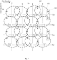
- Case 1 as shown in Fig.2 to Fig.3 , a red sub-pixel 102 or a blue sub-pixel 103 is arranged between every two adjacent pairs of the green sub-pixels 101.
- Case 2 as shown in Fig.4 , a red sub-pixel 102 and a blue sub-pixel 103 are arranged between every two adjacent pairs of the green sub-pixels 101.
- Case 3 as shown in Fig.5 to Fig.7 , two red sub-pixel 102 or two blue sub-pixels 103 are arranged between every two adjacent pairs of the green sub-pixels 101.
- every two adjacent green sub-pixels 101 are arranged in pairs in the first and the second directions.
- One red sub-pixel 102 is arranged between every two adjacent pairs of the green sub-pixels 101 in the first direction
- one blue sub-pixel 103 is arranged between every two adjacent pairs of the green sub-pixels 101 in the second direction.
- all the green sub-pixels 101 are arranged in pairs, and the green sub-pixels 101 in each pair are adjacent to each other.
- all the green sub-pixels 101 are arranged in pairs, and the green sub-pixels 101 in each pair are adjacent to each other.
- One red sub-pixel 102 may be arranged between every two adjacent pairs of the green sub-pixels 101 in the first direction, and one blue sub-pixel 103 may be arranged between every two adjacent pairs of the green sub-pixels 101 in the second direction.
- the red sub-pixel 102 may be replaced by a blue sub-pixel 103. That is, one blue sub-pixel 103 is arranged between every two adjacent pairs of the green sub-pixels 101 in the first direction, and one blue sub-pixel 103 is arranged between every two adjacent pairs of the green sub-pixels 101 in the second direction.
- the red sub-pixel 102 and the blue sub-pixel 103 are both arranged between two adjacent pairs of the green sub-pixels 101, so the density of the sub-pixels may be 1.5 times larger than the density of the pixels.
- a proportion of the amount of the red sub-pixels 102, the green sub-pixels 101 and the blue sub-pixels 103 is 1:2:1.
- every two adjacent blue sub-pixels 103 are arranged in pairs.
- color layers of the two adjacent blue sub-pixels 103 may be connected to each other, and then blue light-emitting layers of the two adjacent blue sub-pixels 103 may be formed by a via-hole, thereby simplifying a manufacturing process.
- the human eyes are least sensitive to the position of the blue sub-pixel 103, and a luminance effect of the blue sub-pixel 103 is also the least, so in a case of a high resolution ratio more than 300ppi for example, the two adjacent blue sub-pixels 103 may be combined as one blue sub-pixel 103 without influencing a display effect.
- every two adjacent blue sub-pixels 103 are combined as one blue sub-pixel and driven by one drive circuit.
- the drive circuit may be a thin film transistor and a relevant circuit connected to the thin film transistor.
- the combined blue sub-pixel 103 still occupies a space of two blue sub-pixels 103. Therefore, the combined blue sub-pixel 103 is still regarded as two blue sub-pixels 103 when calculating the density of the sub-pixels and the density of the pixels.
- each blue sub-pixel 103 is shared by two adjacent pixels.
- the combined blue sub-pixel 103 may be regarded as being shared by two adjacent pixels 10.
- a pixel arrangement structure is provided by some embodiments of the present disclosure.
- the first direction is a horizontal direction and the second direction is a vertical direction.
- the green sub-pixels 101 of each pair of the green sub-pixels 101 are arranged at different sides of a horizontal indicative straight line Xo
- each red sub-pixel 102 between two adjacent pairs of the green sub-pixels 101 is arranged at a side of the horizontal indicative straight line Xo identical to the green sub-pixels 101 at different sides of the red sub-pixel.
- the green sub-pixels 101 of each pair of the green sub-pixels 101 are arranged at the same side of a horizontal indicative straight line Xe, every two adjacent pairs of the green sub-pixels 101 are arranged at different sides of the horizontal indicative straight line Xe, and each red sub-pixel 102 between two adjacent pairs of the green sub-pixels 101 is arranged at the horizontal indicative straight line Xe.
- each column of the pixel array the green sub-pixels 101 of each pair of the green sub-pixels 101 are arranged at different sides of a vertical indicative straight line Y, and each blue sub-pixel 103 between two adjacent pairs of the green sub-pixels 101 is arranged at a side of the vertical indicative straight line Y identical to the green sub-pixel 101 included in the same pixel as the blue sub-pixel 103.
- the horizontal indicative straight lines Xo/Xe and the vertical indicative straight line Y do not exist actually, which are merely to describe a position of each sub-pixel.
- the horizontal indicative straight lines Xo/Xe and the vertical indicative straight line Y form grid lines of the pixel array.
- the horizontal indicative straight lines at the odd-numbered rows of the pixel array are marked as Xo
- the horizontal indicative straight lines at the even-numbered rows of the pixel array are marked as Xe
- the vertical indicative straight lines at the columns of the pixel array are marked as Y.
- a red sub-pixel 102 and a blue sub-pixel 103 are arranged between every two adjacent pairs of the green sub-pixels 101.
- the red sub-pixels 102 and the blue sub-pixels 103 are arranged in the second direction.
- the two adjacent green sub-pixels 101 are arranged in pairs only in the first direction.
- the sub-pixels are arranged circularly in an order of green sub-pixel 101, green sub-pixel 101, red sub-pixel 102 or blue sub-pixel 103, so the density of the sub-pixels is 1.5 times larger than the density of the pixels in the first direction.
- the sub-pixels are arranged circularly in an order of red sub-pixel 102, blue sub-pixel 103, green sub-pixel 101, so the density of the sub-pixels is 1.5 times larger than the density of the pixels in the second direction.
- a proportion of the amount of the red sub-pixels 102, the green sub-pixels 101 and the blue sub-pixels 103 is 1:2:1.
- a pixel arrangement structure is provided by some embodiments of the present disclosure.
- the first direction is a horizontal direction and the second direction is a vertical direction.
- all the green sub-pixels 101 are arranged at a horizontal indicative straight line X.
- every two adjacent green sub-pixels 101 are arranged at different sides of a vertical indicative straight line Y.
- the red sub-pixel 102 and the blue sub-pixel 103 between every two adjacent pairs of the green sub-pixels 101 are arranged between every two adjacent vertical indicative straight lines Y and at different sides of each horizontal indicative straight line X respectively.
- the horizontal indicative straight line X and the vertical indicative straight line Y do not exist actually, which are merely to describe a position of each sub-pixel.
- the horizontal indicative straight line X and the vertical indicative straight line Y form grid lines of the pixel array.
- the horizontal indicative straight lines at the rows of the pixel array are marked as X
- the vertical indicative straight lines at the columns of the pixel array are marked as Y.
- every two adjacent red sub-pixels 102 are arranged in pairs, and every two adjacent blue sub-pixels 103 are arranged in pairs.
- Each pair of the green sub-pixels 101 in the first direction is surrounded by two pairs of the red sub-pixels 102 and two pairs of the blue sub-pixels 103.
- Each pair of the green sub-pixels 101 in the first direction is surrounded by two pairs of the red sub-pixels 102 and two pairs of the blue sub-pixels 103. That is, two pairs of the blue sub-pixels 103 or two pairs of the red sub-pixels 102, or one pair of the blue sub-pixels 103 and one pair of the red sub-pixels 102, are arranged at a left and a right sides of the pair of the green sub-pixels 101; two pairs of the blue sub-pixels 103 or two pairs of the red sub-pixels 102, or one pair of the blue sub-pixels 103 and one pair of the red sub-pixels 102, are arranged at an upper and a lower sides of the pair of the green sub-pixels 101.
- the pairs of blue sub-pixels 103 or the pairs of the red sub-pixels 102, whether arranged at the left and the right sides of the pair of the green sub-pixels 101 or at the upper and the lower sides thereof, are all arranged between every two adjacent pairs of the green sub-pixels 101.
- every two adjacent blue sub-pixels 103 are arranged in pairs, and every two adjacent red sub-pixels 102 are arranged in pairs.
- the color layers of the two blue sub-pixels 103 in each pair the color layers of the red blue sub-pixels 102 in each pair may be connected to each other, and then blue light-emitting layers of the two blue sub-pixels 103 in each pair may be formed by a via-hole and red light-emitting layers of the two red sub-pixels 102 in each pair may be formed by a via-hole, thereby simplifying a manufacturing process of the color layers of the blue sub-pixels 103 and the red sub-pixels 102 to some extent.
- the density of the sub-pixels is 1.5 times larger than the density of the pixels in both the first and the second directions.
- a proportion of the amount of the red sub-pixels 102, the green sub-pixels 101 and the blue sub-pixels 103 is 1:2:1.
- every two adjacent blue sub-pixels 103 are combined as one blue sub-pixel and driven by one drive circuit.
- the human eyes are least sensitive to the position of the blue sub-pixel 103, and a luminance effect of the blue sub-pixel 103 is also the least, so in a case of a high resolution ratio more than 300ppi for example, the two adjacent blue sub-pixels 103 may be combined as one blue sub-pixel 103 without influencing a display effect, and the two adjacent blue sub-pixels 103 may be driven by one drive circuit, thereby simplifying a manufacturing process of the drive circuit.
- every two adjacent red sub-pixels 102 are combined as one red sub-pixel and driven by one drive circuit.
- the manufacturing process of the drive circuit may be simplified further.
- the combined blue sub-pixel 103 still occupies a space of two blue sub-pixels 103. Therefore, the combined blue sub-pixel 103 is still regarded as two blue sub-pixels 103 when calculating the density of the sub-pixels and the density of the pixels.
- a pixel arrangement structure is provided by some embodiments of the present disclosure.
- the first direction is a horizontal direction and the second direction is a vertical direction.
- all the green sub-pixels 101 are arranged at horizontal indicative straight lines Xo/Xe.
- every two adjacent green sub-pixels 101 are arranged at different sides of a vertical indicative straight line Y.
- Each pair of the red sub-pixels 102 is arranged between every two adjacent vertical indicative straight lines Y, and the red sub-pixels 102 of each pair of the red sub-pixels 102 are arranged at different sides of the horizontal indicative straight line Xe in each even-numbered row respectively.
- Each pair of the blue sub-pixels 103 is arranged between every two adjacent vertical indicative straight lines Y, and the blue sub-pixels 103 of each pair of the blue sub-pixels 103 are arranged at different sides of the horizontal indicative straight line Xo in each odd-numbered row respectively.
- the horizontal indicative straight lines Xo/Xe and the vertical indicative straight line Y do not exist actually, which are merely to describe a position of each sub-pixel.
- the horizontal indicative straight lines Xo/Xe and the vertical indicative straight line Y form grid lines of the pixel array.
- the horizontal indicative straight lines at the odd-numbered rows of the pixel array are marked as Xo
- the horizontal indicative straight lines at the even-numbered rows of the pixel array are marked as Xe
- the vertical indicative straight lines at the columns of the pixel array are marked as Y.
- a display panel is provided by some embodiments of the present disclosure, wherein pixels of the display panel are arranged according to the pixel arrangement structure hereinabove.
- a display device is further provided by some embodiments of the present disclosure, including the display panel hereinabove.
- the pixel arrangement structure provided by some embodiments of the present disclosure may be applied to any display device (e.g., liquid crystal display (LCD), organic light-emitting diode (OLED)) including three sub-pixels such as red, green and blue sub-pixels.
- LCD liquid crystal display
- OLED organic light-emitting diode
Landscapes
- Physics & Mathematics (AREA)
- Nonlinear Science (AREA)
- Mathematical Physics (AREA)
- Chemical & Material Sciences (AREA)
- Crystallography & Structural Chemistry (AREA)
- General Physics & Mathematics (AREA)
- Optics & Photonics (AREA)
- Geometry (AREA)
- Engineering & Computer Science (AREA)
- Microelectronics & Electronic Packaging (AREA)
- Devices For Indicating Variable Information By Combining Individual Elements (AREA)
- Electroluminescent Light Sources (AREA)
- Liquid Crystal (AREA)
Applications Claiming Priority (2)
| Application Number | Priority Date | Filing Date | Title |
|---|---|---|---|
| CN201510080570.0A CN104597655B (zh) | 2015-02-13 | 2015-02-13 | 一种像素排列结构、显示面板及显示装置 |
| PCT/CN2015/085510 WO2016127593A1 (fr) | 2015-02-13 | 2015-07-30 | Structure d'agencement de pixels, panneau d'affichage et dispositif d'affichage |
Publications (3)
| Publication Number | Publication Date |
|---|---|
| EP3270216A1 true EP3270216A1 (fr) | 2018-01-17 |
| EP3270216A4 EP3270216A4 (fr) | 2018-12-12 |
| EP3270216B1 EP3270216B1 (fr) | 2024-02-21 |
Family
ID=53123546
Family Applications (1)
| Application Number | Title | Priority Date | Filing Date |
|---|---|---|---|
| EP15837127.8A Active EP3270216B1 (fr) | 2015-02-13 | 2015-07-30 | Structure d'agencement de pixels, panneau d'affichage et dispositif d'affichage |
Country Status (6)
| Country | Link |
|---|---|
| US (1) | US9946123B2 (fr) |
| EP (1) | EP3270216B1 (fr) |
| JP (1) | JP6624698B2 (fr) |
| KR (1) | KR101755271B1 (fr) |
| CN (1) | CN104597655B (fr) |
| WO (1) | WO2016127593A1 (fr) |
Cited By (7)
| Publication number | Priority date | Publication date | Assignee | Title |
|---|---|---|---|---|
| EP3832732A1 (fr) * | 2016-02-18 | 2021-06-09 | BOE Technology Group Co., Ltd. | Structure d'agencement de pixels et panneau d'affichage |
| US11069286B2 (en) | 2018-02-09 | 2021-07-20 | Boe Technology Group Co., Ltd. | Color compensation method, compensation device, and display device |
| US11233096B2 (en) | 2016-02-18 | 2022-01-25 | Boe Technology Group Co., Ltd. | Pixel arrangement structure and driving method thereof, display substrate and display device |
| US11264430B2 (en) | 2016-02-18 | 2022-03-01 | Chengdu Boe Optoelectronics Technology Co., Ltd. | Pixel arrangement structure with misaligned repeating units, display substrate, display apparatus and method of fabrication thereof |
| US11448807B2 (en) | 2016-02-18 | 2022-09-20 | Chengdu Boe Optoelectronics Technology Co., Ltd. | Display substrate, fine metal mask set and manufacturing method thereof |
| US11735108B2 (en) | 2019-07-31 | 2023-08-22 | Boe Technology Group Co., Ltd. | Display substrate and preparation method thereof, display panel, and display device |
| US11747531B2 (en) | 2016-02-18 | 2023-09-05 | Chengdu Boe Optoelectronics Technology Co., Ltd. | Display substrate, fine metal mask set and manufacturing method thereof |
Families Citing this family (44)
| Publication number | Priority date | Publication date | Assignee | Title |
|---|---|---|---|---|
| CN104375302B (zh) * | 2014-10-27 | 2020-09-08 | 上海中航光电子有限公司 | 一种像素结构、显示面板及其像素补偿方法 |
| CN104597655B (zh) | 2015-02-13 | 2017-06-27 | 京东方科技集团股份有限公司 | 一种像素排列结构、显示面板及显示装置 |
| CN106486514B (zh) * | 2015-08-31 | 2023-12-01 | 昆山国显光电有限公司 | 像素结构以及oled显示面板 |
| CN105304678B (zh) * | 2015-09-25 | 2018-11-16 | 上海和辉光电有限公司 | 有机发光二极管显示面板的像素排列结构及掩膜板 |
| CN107644888B (zh) * | 2016-07-22 | 2025-01-10 | 京东方科技集团股份有限公司 | 像素排列结构、显示基板、显示装置、制作方法及掩膜版 |
| US10854684B2 (en) | 2016-02-18 | 2020-12-01 | Boe Technology Group Co., Ltd. | Pixel arrangement structure and driving method thereof, display substrate and display device |
| CN110137213B (zh) | 2018-02-09 | 2025-03-25 | 京东方科技集团股份有限公司 | 像素排列结构及其显示方法、显示基板 |
| CN110133899A (zh) | 2018-02-09 | 2019-08-16 | 京东方科技集团股份有限公司 | 像素排列结构、显示基板、显示装置 |
| CN110137215B (zh) | 2018-02-09 | 2025-01-14 | 京东方科技集团股份有限公司 | 像素排列结构、显示基板和显示装置 |
| US10600213B2 (en) * | 2016-02-27 | 2020-03-24 | Focal Sharp, Inc. | Method and apparatus for color-preserving spectrum reshape |
| CN107275359B (zh) | 2016-04-08 | 2021-08-13 | 乐金显示有限公司 | 有机发光显示装置 |
| KR102692417B1 (ko) * | 2016-04-29 | 2024-08-05 | 엘지디스플레이 주식회사 | 유기 발광 표시 장치 |
| KR101698718B1 (ko) * | 2016-04-29 | 2017-01-20 | 엘지디스플레이 주식회사 | 유기 발광 표시 장치 |
| CN107887404B (zh) * | 2016-09-29 | 2020-04-07 | 昆山国显光电有限公司 | Amoled像素结构及显示装置 |
| CN107221555B (zh) * | 2017-06-21 | 2019-02-26 | 深圳市华星光电半导体显示技术有限公司 | Oled显示面板以及显示装置 |
| CN107731093B (zh) * | 2017-09-12 | 2019-08-20 | 维沃移动通信有限公司 | 一种像素排列结构、显示面板及移动终端 |
| WO2019062236A1 (fr) | 2017-09-30 | 2019-04-04 | 昆山国显光电有限公司 | Écran d'affichage, procédé d'attaque d'écran d'affichage et dispositif d'affichage correspondant |
| WO2019062221A1 (fr) * | 2017-09-30 | 2019-04-04 | 云谷(固安)科技有限公司 | Écran d'affichage et dispositif d'affichage |
| CN108269840B (zh) * | 2017-09-30 | 2021-08-13 | 昆山国显光电有限公司 | 显示屏及显示装置 |
| CN108364967B (zh) * | 2017-09-30 | 2021-07-27 | 昆山国显光电有限公司 | 显示屏及显示装置 |
| CN108461521A (zh) * | 2017-09-30 | 2018-08-28 | 昆山国显光电有限公司 | 显示屏及显示装置 |
| CN114994973B (zh) | 2018-02-09 | 2023-04-28 | 京东方科技集团股份有限公司 | 显示基板和显示装置 |
| CN110137212B (zh) * | 2018-02-09 | 2022-05-27 | 京东方科技集团股份有限公司 | 像素排列结构、显示基板以及显示装置 |
| US11574960B2 (en) | 2018-02-09 | 2023-02-07 | Boe Technology Group Co., Ltd. | Pixel arrangement structure, display substrate, display device and mask plate group |
| CN109037302A (zh) * | 2018-09-13 | 2018-12-18 | 武汉华星光电半导体显示技术有限公司 | 像素排列结构及显示装置 |
| CN113823240B (zh) | 2018-12-13 | 2023-04-18 | 京东方科技集团股份有限公司 | 显示装置 |
| CN110288946B (zh) * | 2019-06-25 | 2021-10-15 | 荣耀终端有限公司 | 移动终端及其驱动方法、显示模组、驱动芯片 |
| CN110189683A (zh) * | 2019-06-26 | 2019-08-30 | 京东方科技集团股份有限公司 | 一种显示面板、其驱动方法及显示装置 |
| CN112673476B (zh) | 2019-07-31 | 2025-12-30 | 京东方科技集团股份有限公司 | 显示基板和显示装置 |
| KR20210016141A (ko) * | 2019-07-31 | 2021-02-15 | 삼성디스플레이 주식회사 | 디스플레이 패널 |
| US11367377B2 (en) * | 2019-08-02 | 2022-06-21 | Tianma Japan, Ltd. | Display device |
| JP7572160B2 (ja) * | 2019-08-02 | 2024-10-23 | Tianma Japan株式会社 | 表示装置 |
| US12266303B2 (en) | 2019-08-23 | 2025-04-01 | Boe Technology Group Co., Ltd. | Display device and manufacturing method thereof |
| CN112840461B (zh) | 2019-08-23 | 2025-02-25 | 京东方科技集团股份有限公司 | 显示面板及其制造方法、显示装置 |
| EP4020449B1 (fr) | 2019-08-23 | 2025-06-25 | BOE Technology Group Co., Ltd. | Dispositif d'affichage et son procédé de fabrication |
| CN112703604B (zh) | 2019-08-23 | 2024-06-18 | 京东方科技集团股份有限公司 | 显示装置及其制备方法 |
| CN110580872B (zh) * | 2019-09-29 | 2022-08-26 | 武汉天马微电子有限公司 | 一种显示面板和显示装置 |
| CN112649994B (zh) * | 2020-12-28 | 2022-09-13 | 视涯科技股份有限公司 | 阵列基板的设计方法、阵列基板、显示面板及显示装置 |
| CN112817187A (zh) * | 2021-02-05 | 2021-05-18 | 武汉华星光电技术有限公司 | 显示面板及显示装置 |
| US20240206272A1 (en) * | 2021-03-16 | 2024-06-20 | Boe Technology Group Co., Ltd. | Array substrate and display device |
| KR102876468B1 (ko) | 2021-03-23 | 2025-10-27 | 삼성디스플레이 주식회사 | 표시 장치 |
| CN114360443B (zh) * | 2021-11-30 | 2023-06-06 | 深圳市洲明科技股份有限公司 | 子像素渲染方法、装置和计算机设备 |
| CN114879397B (zh) * | 2022-05-23 | 2023-05-09 | 重庆惠科金渝光电科技有限公司 | 显示面板、显示面板的驱动方法和显示装置 |
| CN117672123B (zh) * | 2023-12-11 | 2025-11-11 | 佛山市国星光电股份有限公司 | 次级像素排布结构、虚拟像素排布结构及复用控制方法 |
Family Cites Families (22)
| Publication number | Priority date | Publication date | Assignee | Title |
|---|---|---|---|---|
| JPS60120398A (ja) | 1983-12-02 | 1985-06-27 | シチズン時計株式会社 | マトリクス形カラー表示装置の駆動方法 |
| JP3547015B2 (ja) * | 1993-01-07 | 2004-07-28 | ソニー株式会社 | 画像表示装置および画像表示装置の解像度改善方法 |
| JP2005091875A (ja) * | 2003-09-18 | 2005-04-07 | Nippon Hoso Kyokai <Nhk> | 表示装置及び表示方法 |
| CN100478757C (zh) * | 2004-08-05 | 2009-04-15 | 奇美电子股份有限公司 | 彩色滤光装置、显示方法及其应用 |
| US7907133B2 (en) * | 2006-04-13 | 2011-03-15 | Daktronics, Inc. | Pixel interleaving configurations for use in high definition electronic sign displays |
| JP4721460B2 (ja) * | 2007-02-02 | 2011-07-13 | キヤノン株式会社 | 表示装置及びその製造方法 |
| US8330152B2 (en) * | 2009-12-02 | 2012-12-11 | Universal Display Corporation | OLED display architecture with improved aperture ratio |
| US9041625B2 (en) | 2010-04-21 | 2015-05-26 | Lg Display Co., Ltd. | Subpixel arrangement structure for a display device and display device |
| KR101189025B1 (ko) * | 2010-05-31 | 2012-10-08 | 삼성디스플레이 주식회사 | 유기전계발광 표시장치의 화소배열구조 |
| CN103185995B (zh) * | 2011-12-30 | 2016-03-16 | 上海中航光电子有限公司 | 一种双栅极驱动的横向排列的像素结构及液晶显示装置 |
| KR101615332B1 (ko) | 2012-03-06 | 2016-04-26 | 삼성디스플레이 주식회사 | 유기 발광 표시 장치의 화소 배열 구조 |
| KR102063973B1 (ko) * | 2012-09-12 | 2020-01-09 | 삼성디스플레이 주식회사 | 유기전계발광 표시장치 및 그의 구동방법 |
| EP3780113B1 (fr) | 2012-09-13 | 2025-07-16 | Samsung Display Co., Ltd. | Structure de disposition de pixels pour dispositif d'affichage à diodes électroluminescentes organiques |
| US20140111115A1 (en) * | 2012-10-22 | 2014-04-24 | Motorola Mobility Llc | Display devices having non-uniform sub-pixel spacing and methods therefor |
| CN103278960B (zh) * | 2012-12-31 | 2015-11-25 | 上海天马微电子有限公司 | 一种三色像素结构、彩膜基板及液晶显示器 |
| KR102030799B1 (ko) * | 2013-03-11 | 2019-10-11 | 삼성디스플레이 주식회사 | 유기발광표시장치 |
| CN104282230B (zh) * | 2013-07-10 | 2017-04-05 | 上海和辉光电有限公司 | 像素阵列及具有该像素阵列的平面显示器 |
| CN103325315B (zh) * | 2013-07-10 | 2015-09-16 | 上海和辉光电有限公司 | 像素阵列及具有该像素阵列的显示器 |
| US9262961B2 (en) | 2013-08-30 | 2016-02-16 | Au Optronics Corporation | Pixel arrangement of color display apparatus |
| CN104037202B (zh) * | 2014-06-12 | 2017-08-04 | 上海和辉光电有限公司 | 一种amoled显示器件及其子像素结构的制备方法 |
| CN104282727B (zh) * | 2014-09-30 | 2017-08-29 | 京东方科技集团股份有限公司 | 一种像素结构及其显示方法、显示装置 |
| CN104597655B (zh) * | 2015-02-13 | 2017-06-27 | 京东方科技集团股份有限公司 | 一种像素排列结构、显示面板及显示装置 |
-
2015
- 2015-02-13 CN CN201510080570.0A patent/CN104597655B/zh active Active
- 2015-07-30 JP JP2017560851A patent/JP6624698B2/ja active Active
- 2015-07-30 US US14/917,200 patent/US9946123B2/en active Active
- 2015-07-30 EP EP15837127.8A patent/EP3270216B1/fr active Active
- 2015-07-30 WO PCT/CN2015/085510 patent/WO2016127593A1/fr not_active Ceased
- 2015-07-30 KR KR1020167005052A patent/KR101755271B1/ko active Active
Cited By (12)
| Publication number | Priority date | Publication date | Assignee | Title |
|---|---|---|---|---|
| EP3832732A1 (fr) * | 2016-02-18 | 2021-06-09 | BOE Technology Group Co., Ltd. | Structure d'agencement de pixels et panneau d'affichage |
| US11233096B2 (en) | 2016-02-18 | 2022-01-25 | Boe Technology Group Co., Ltd. | Pixel arrangement structure and driving method thereof, display substrate and display device |
| US11264430B2 (en) | 2016-02-18 | 2022-03-01 | Chengdu Boe Optoelectronics Technology Co., Ltd. | Pixel arrangement structure with misaligned repeating units, display substrate, display apparatus and method of fabrication thereof |
| US11448807B2 (en) | 2016-02-18 | 2022-09-20 | Chengdu Boe Optoelectronics Technology Co., Ltd. | Display substrate, fine metal mask set and manufacturing method thereof |
| US11747531B2 (en) | 2016-02-18 | 2023-09-05 | Chengdu Boe Optoelectronics Technology Co., Ltd. | Display substrate, fine metal mask set and manufacturing method thereof |
| US12001035B2 (en) | 2016-02-18 | 2024-06-04 | Chengdu Boe Optoelectronics Technology Co., Ltd. | Display substrate and display device |
| US12058910B2 (en) | 2016-02-18 | 2024-08-06 | Boe Technology Group Co., Ltd. | Pixel arrangement structure and driving method thereof, display substrate and display device |
| US12196988B2 (en) | 2016-02-18 | 2025-01-14 | Chengdu Boe Optoelectronics Technology Co., Ltd. | Display substrate and display device |
| US12593588B2 (en) | 2016-02-18 | 2026-03-31 | Boe Technology Group Co., Ltd. | Display substrate |
| US11069286B2 (en) | 2018-02-09 | 2021-07-20 | Boe Technology Group Co., Ltd. | Color compensation method, compensation device, and display device |
| US11735108B2 (en) | 2019-07-31 | 2023-08-22 | Boe Technology Group Co., Ltd. | Display substrate and preparation method thereof, display panel, and display device |
| US12300179B2 (en) | 2019-07-31 | 2025-05-13 | Boe Technology Group Co., Ltd. | Display substrate and preparation method thereof, display panel, and display device |
Also Published As
| Publication number | Publication date |
|---|---|
| US20160357076A1 (en) | 2016-12-08 |
| JP2018512627A (ja) | 2018-05-17 |
| EP3270216B1 (fr) | 2024-02-21 |
| US9946123B2 (en) | 2018-04-17 |
| JP6624698B2 (ja) | 2019-12-25 |
| KR101755271B1 (ko) | 2017-07-07 |
| EP3270216A4 (fr) | 2018-12-12 |
| KR20160111899A (ko) | 2016-09-27 |
| CN104597655B (zh) | 2017-06-27 |
| WO2016127593A1 (fr) | 2016-08-18 |
| CN104597655A (zh) | 2015-05-06 |
Similar Documents
| Publication | Publication Date | Title |
|---|---|---|
| US9946123B2 (en) | Pixel arrangement structure, display panel and display device | |
| JP7633334B2 (ja) | 画素配列構造、表示パネル及び表示装置 | |
| CN108701708B (zh) | 像素排列结构、显示面板及显示装置 | |
| US9543285B2 (en) | Display panel | |
| CN103472608B (zh) | 显示面板的像素与子像素配置 | |
| CN110364558B (zh) | 像素排布结构及显示面板 | |
| US10535718B2 (en) | Pixel arrangement of OLED display panel, and OLED display panel | |
| US9735207B2 (en) | Display substrate and driving method thereof, display apparatus | |
| EP3382683B1 (fr) | Afficheur | |
| EP3286751B1 (fr) | Structure de pixels, écran d'affichage et appareil d'affichage | |
| KR101970088B1 (ko) | 디스플레이 스크린 및 이의 구동 방법 | |
| JP5779124B2 (ja) | 表示装置および電子機器 | |
| JP2017533475A (ja) | ピクセル構造およびその表示方法、表示装置 | |
| CN105445949B (zh) | 一种三维显示装置 | |
| US9601082B2 (en) | Display substrate and driving method thereof and display device | |
| US9655201B2 (en) | Pixel arrangement structure for organic light-emitting diode display panel | |
| CN106530989A (zh) | 一种像素排列结构、显示面板及显示装置 | |
| US10140898B2 (en) | Multi-view display device and method for driving the same | |
| CN104460018A (zh) | 一种3d显示装置 | |
| CN110212010B (zh) | 像素排布结构及显示面板 | |
| CN204496112U (zh) | 一种3d显示装置 | |
| CN105957488A (zh) | 像素阵列及其驱动方法、显示面板及显示装置 |
Legal Events
| Date | Code | Title | Description |
|---|---|---|---|
| STAA | Information on the status of an ep patent application or granted ep patent |
Free format text: STATUS: THE INTERNATIONAL PUBLICATION HAS BEEN MADE |
|
| PUAI | Public reference made under article 153(3) epc to a published international application that has entered the european phase |
Free format text: ORIGINAL CODE: 0009012 |
|
| STAA | Information on the status of an ep patent application or granted ep patent |
Free format text: STATUS: REQUEST FOR EXAMINATION WAS MADE |
|
| 17P | Request for examination filed |
Effective date: 20160307 |
|
| AK | Designated contracting states |
Kind code of ref document: A1 Designated state(s): AL AT BE BG CH CY CZ DE DK EE ES FI FR GB GR HR HU IE IS IT LI LT LU LV MC MK MT NL NO PL PT RO RS SE SI SK SM TR |
|
| AX | Request for extension of the european patent |
Extension state: BA ME |
|
| R17P | Request for examination filed (corrected) |
Effective date: 20160307 |
|
| DAV | Request for validation of the european patent (deleted) | ||
| DAX | Request for extension of the european patent (deleted) | ||
| A4 | Supplementary search report drawn up and despatched |
Effective date: 20181114 |
|
| RIC1 | Information provided on ipc code assigned before grant |
Ipc: H01L 27/32 20060101ALI20181106BHEP Ipc: G02F 1/1343 20060101AFI20181106BHEP Ipc: G09G 3/00 20060101ALI20181106BHEP |
|
| STAA | Information on the status of an ep patent application or granted ep patent |
Free format text: STATUS: EXAMINATION IS IN PROGRESS |
|
| 17Q | First examination report despatched |
Effective date: 20200420 |
|
| REG | Reference to a national code |
Ref country code: DE Ref legal event code: R079 Ref document number: 602015087651 Country of ref document: DE Free format text: PREVIOUS MAIN CLASS: G02F0001133500 Ipc: G02F0001134300 Ref country code: DE Ref legal event code: R079 Free format text: PREVIOUS MAIN CLASS: G02F0001133500 Ipc: G02F0001134300 |
|
| GRAP | Despatch of communication of intention to grant a patent |
Free format text: ORIGINAL CODE: EPIDOSNIGR1 |
|
| STAA | Information on the status of an ep patent application or granted ep patent |
Free format text: STATUS: GRANT OF PATENT IS INTENDED |
|
| RIC1 | Information provided on ipc code assigned before grant |
Ipc: G09G 3/00 20060101ALI20231108BHEP Ipc: G02F 1/1343 20060101AFI20231108BHEP |
|
| INTG | Intention to grant announced |
Effective date: 20231123 |
|
| GRAS | Grant fee paid |
Free format text: ORIGINAL CODE: EPIDOSNIGR3 |
|
| GRAA | (expected) grant |
Free format text: ORIGINAL CODE: 0009210 |
|
| STAA | Information on the status of an ep patent application or granted ep patent |
Free format text: STATUS: THE PATENT HAS BEEN GRANTED |
|
| AK | Designated contracting states |
Kind code of ref document: B1 Designated state(s): AL AT BE BG CH CY CZ DE DK EE ES FI FR GB GR HR HU IE IS IT LI LT LU LV MC MK MT NL NO PL PT RO RS SE SI SK SM TR |
|
| REG | Reference to a national code |
Ref country code: GB Ref legal event code: FG4D |
|
| REG | Reference to a national code |
Ref country code: CH Ref legal event code: EP |
|
| REG | Reference to a national code |
Ref country code: DE Ref legal event code: R096 Ref document number: 602015087651 Country of ref document: DE |
|
| REG | Reference to a national code |
Ref country code: IE Ref legal event code: FG4D |
|
| REG | Reference to a national code |
Ref country code: NL Ref legal event code: FP |
|
| REG | Reference to a national code |
Ref country code: LT Ref legal event code: MG9D |
|
| PG25 | Lapsed in a contracting state [announced via postgrant information from national office to epo] |
Ref country code: IS Free format text: LAPSE BECAUSE OF FAILURE TO SUBMIT A TRANSLATION OF THE DESCRIPTION OR TO PAY THE FEE WITHIN THE PRESCRIBED TIME-LIMIT Effective date: 20240621 |
|
| PG25 | Lapsed in a contracting state [announced via postgrant information from national office to epo] |
Ref country code: LT Free format text: LAPSE BECAUSE OF FAILURE TO SUBMIT A TRANSLATION OF THE DESCRIPTION OR TO PAY THE FEE WITHIN THE PRESCRIBED TIME-LIMIT Effective date: 20240221 |
|
| PG25 | Lapsed in a contracting state [announced via postgrant information from national office to epo] |
Ref country code: GR Free format text: LAPSE BECAUSE OF FAILURE TO SUBMIT A TRANSLATION OF THE DESCRIPTION OR TO PAY THE FEE WITHIN THE PRESCRIBED TIME-LIMIT Effective date: 20240522 |
|
| REG | Reference to a national code |
Ref country code: AT Ref legal event code: MK05 Ref document number: 1659609 Country of ref document: AT Kind code of ref document: T Effective date: 20240221 |
|
| PG25 | Lapsed in a contracting state [announced via postgrant information from national office to epo] |
Ref country code: HR Free format text: LAPSE BECAUSE OF FAILURE TO SUBMIT A TRANSLATION OF THE DESCRIPTION OR TO PAY THE FEE WITHIN THE PRESCRIBED TIME-LIMIT Effective date: 20240221 Ref country code: RS Free format text: LAPSE BECAUSE OF FAILURE TO SUBMIT A TRANSLATION OF THE DESCRIPTION OR TO PAY THE FEE WITHIN THE PRESCRIBED TIME-LIMIT Effective date: 20240521 |
|
| PG25 | Lapsed in a contracting state [announced via postgrant information from national office to epo] |
Ref country code: ES Free format text: LAPSE BECAUSE OF FAILURE TO SUBMIT A TRANSLATION OF THE DESCRIPTION OR TO PAY THE FEE WITHIN THE PRESCRIBED TIME-LIMIT Effective date: 20240221 |
|
| PG25 | Lapsed in a contracting state [announced via postgrant information from national office to epo] |
Ref country code: AT Free format text: LAPSE BECAUSE OF FAILURE TO SUBMIT A TRANSLATION OF THE DESCRIPTION OR TO PAY THE FEE WITHIN THE PRESCRIBED TIME-LIMIT Effective date: 20240221 |
|
| PG25 | Lapsed in a contracting state [announced via postgrant information from national office to epo] |
Ref country code: RS Free format text: LAPSE BECAUSE OF FAILURE TO SUBMIT A TRANSLATION OF THE DESCRIPTION OR TO PAY THE FEE WITHIN THE PRESCRIBED TIME-LIMIT Effective date: 20240521 Ref country code: NO Free format text: LAPSE BECAUSE OF FAILURE TO SUBMIT A TRANSLATION OF THE DESCRIPTION OR TO PAY THE FEE WITHIN THE PRESCRIBED TIME-LIMIT Effective date: 20240521 Ref country code: LT Free format text: LAPSE BECAUSE OF FAILURE TO SUBMIT A TRANSLATION OF THE DESCRIPTION OR TO PAY THE FEE WITHIN THE PRESCRIBED TIME-LIMIT Effective date: 20240221 Ref country code: IS Free format text: LAPSE BECAUSE OF FAILURE TO SUBMIT A TRANSLATION OF THE DESCRIPTION OR TO PAY THE FEE WITHIN THE PRESCRIBED TIME-LIMIT Effective date: 20240621 Ref country code: HR Free format text: LAPSE BECAUSE OF FAILURE TO SUBMIT A TRANSLATION OF THE DESCRIPTION OR TO PAY THE FEE WITHIN THE PRESCRIBED TIME-LIMIT Effective date: 20240221 Ref country code: GR Free format text: LAPSE BECAUSE OF FAILURE TO SUBMIT A TRANSLATION OF THE DESCRIPTION OR TO PAY THE FEE WITHIN THE PRESCRIBED TIME-LIMIT Effective date: 20240522 Ref country code: FI Free format text: LAPSE BECAUSE OF FAILURE TO SUBMIT A TRANSLATION OF THE DESCRIPTION OR TO PAY THE FEE WITHIN THE PRESCRIBED TIME-LIMIT Effective date: 20240221 Ref country code: ES Free format text: LAPSE BECAUSE OF FAILURE TO SUBMIT A TRANSLATION OF THE DESCRIPTION OR TO PAY THE FEE WITHIN THE PRESCRIBED TIME-LIMIT Effective date: 20240221 Ref country code: BG Free format text: LAPSE BECAUSE OF FAILURE TO SUBMIT A TRANSLATION OF THE DESCRIPTION OR TO PAY THE FEE WITHIN THE PRESCRIBED TIME-LIMIT Effective date: 20240221 Ref country code: AT Free format text: LAPSE BECAUSE OF FAILURE TO SUBMIT A TRANSLATION OF THE DESCRIPTION OR TO PAY THE FEE WITHIN THE PRESCRIBED TIME-LIMIT Effective date: 20240221 |
|
| PG25 | Lapsed in a contracting state [announced via postgrant information from national office to epo] |
Ref country code: PT Free format text: LAPSE BECAUSE OF FAILURE TO SUBMIT A TRANSLATION OF THE DESCRIPTION OR TO PAY THE FEE WITHIN THE PRESCRIBED TIME-LIMIT Effective date: 20240621 Ref country code: PL Free format text: LAPSE BECAUSE OF FAILURE TO SUBMIT A TRANSLATION OF THE DESCRIPTION OR TO PAY THE FEE WITHIN THE PRESCRIBED TIME-LIMIT Effective date: 20240221 |
|
| PG25 | Lapsed in a contracting state [announced via postgrant information from national office to epo] |
Ref country code: SE Free format text: LAPSE BECAUSE OF FAILURE TO SUBMIT A TRANSLATION OF THE DESCRIPTION OR TO PAY THE FEE WITHIN THE PRESCRIBED TIME-LIMIT Effective date: 20240221 Ref country code: PT Free format text: LAPSE BECAUSE OF FAILURE TO SUBMIT A TRANSLATION OF THE DESCRIPTION OR TO PAY THE FEE WITHIN THE PRESCRIBED TIME-LIMIT Effective date: 20240621 Ref country code: PL Free format text: LAPSE BECAUSE OF FAILURE TO SUBMIT A TRANSLATION OF THE DESCRIPTION OR TO PAY THE FEE WITHIN THE PRESCRIBED TIME-LIMIT Effective date: 20240221 Ref country code: LV Free format text: LAPSE BECAUSE OF FAILURE TO SUBMIT A TRANSLATION OF THE DESCRIPTION OR TO PAY THE FEE WITHIN THE PRESCRIBED TIME-LIMIT Effective date: 20240221 |
|
| PG25 | Lapsed in a contracting state [announced via postgrant information from national office to epo] |
Ref country code: DK Free format text: LAPSE BECAUSE OF FAILURE TO SUBMIT A TRANSLATION OF THE DESCRIPTION OR TO PAY THE FEE WITHIN THE PRESCRIBED TIME-LIMIT Effective date: 20240221 |
|
| PG25 | Lapsed in a contracting state [announced via postgrant information from national office to epo] |
Ref country code: SM Free format text: LAPSE BECAUSE OF FAILURE TO SUBMIT A TRANSLATION OF THE DESCRIPTION OR TO PAY THE FEE WITHIN THE PRESCRIBED TIME-LIMIT Effective date: 20240221 |
|
| PG25 | Lapsed in a contracting state [announced via postgrant information from national office to epo] |
Ref country code: EE Free format text: LAPSE BECAUSE OF FAILURE TO SUBMIT A TRANSLATION OF THE DESCRIPTION OR TO PAY THE FEE WITHIN THE PRESCRIBED TIME-LIMIT Effective date: 20240221 Ref country code: CZ Free format text: LAPSE BECAUSE OF FAILURE TO SUBMIT A TRANSLATION OF THE DESCRIPTION OR TO PAY THE FEE WITHIN THE PRESCRIBED TIME-LIMIT Effective date: 20240221 |
|
| PG25 | Lapsed in a contracting state [announced via postgrant information from national office to epo] |
Ref country code: SK Free format text: LAPSE BECAUSE OF FAILURE TO SUBMIT A TRANSLATION OF THE DESCRIPTION OR TO PAY THE FEE WITHIN THE PRESCRIBED TIME-LIMIT Effective date: 20240221 |
|
| PG25 | Lapsed in a contracting state [announced via postgrant information from national office to epo] |
Ref country code: SM Free format text: LAPSE BECAUSE OF FAILURE TO SUBMIT A TRANSLATION OF THE DESCRIPTION OR TO PAY THE FEE WITHIN THE PRESCRIBED TIME-LIMIT Effective date: 20240221 Ref country code: SK Free format text: LAPSE BECAUSE OF FAILURE TO SUBMIT A TRANSLATION OF THE DESCRIPTION OR TO PAY THE FEE WITHIN THE PRESCRIBED TIME-LIMIT Effective date: 20240221 Ref country code: RO Free format text: LAPSE BECAUSE OF FAILURE TO SUBMIT A TRANSLATION OF THE DESCRIPTION OR TO PAY THE FEE WITHIN THE PRESCRIBED TIME-LIMIT Effective date: 20240221 Ref country code: EE Free format text: LAPSE BECAUSE OF FAILURE TO SUBMIT A TRANSLATION OF THE DESCRIPTION OR TO PAY THE FEE WITHIN THE PRESCRIBED TIME-LIMIT Effective date: 20240221 Ref country code: DK Free format text: LAPSE BECAUSE OF FAILURE TO SUBMIT A TRANSLATION OF THE DESCRIPTION OR TO PAY THE FEE WITHIN THE PRESCRIBED TIME-LIMIT Effective date: 20240221 Ref country code: CZ Free format text: LAPSE BECAUSE OF FAILURE TO SUBMIT A TRANSLATION OF THE DESCRIPTION OR TO PAY THE FEE WITHIN THE PRESCRIBED TIME-LIMIT Effective date: 20240221 |
|
| REG | Reference to a national code |
Ref country code: DE Ref legal event code: R097 Ref document number: 602015087651 Country of ref document: DE |
|
| PG25 | Lapsed in a contracting state [announced via postgrant information from national office to epo] |
Ref country code: IT Free format text: LAPSE BECAUSE OF FAILURE TO SUBMIT A TRANSLATION OF THE DESCRIPTION OR TO PAY THE FEE WITHIN THE PRESCRIBED TIME-LIMIT Effective date: 20240221 |
|
| PLBE | No opposition filed within time limit |
Free format text: ORIGINAL CODE: 0009261 |
|
| STAA | Information on the status of an ep patent application or granted ep patent |
Free format text: STATUS: NO OPPOSITION FILED WITHIN TIME LIMIT |
|
| PG25 | Lapsed in a contracting state [announced via postgrant information from national office to epo] |
Ref country code: IT Free format text: LAPSE BECAUSE OF FAILURE TO SUBMIT A TRANSLATION OF THE DESCRIPTION OR TO PAY THE FEE WITHIN THE PRESCRIBED TIME-LIMIT Effective date: 20240221 |
|
| 26N | No opposition filed |
Effective date: 20241122 |
|
| PG25 | Lapsed in a contracting state [announced via postgrant information from national office to epo] |
Ref country code: MC Free format text: LAPSE BECAUSE OF FAILURE TO SUBMIT A TRANSLATION OF THE DESCRIPTION OR TO PAY THE FEE WITHIN THE PRESCRIBED TIME-LIMIT Effective date: 20240221 |
|
| REG | Reference to a national code |
Ref country code: CH Ref legal event code: PL |
|
| PG25 | Lapsed in a contracting state [announced via postgrant information from national office to epo] |
Ref country code: LU Free format text: LAPSE BECAUSE OF NON-PAYMENT OF DUE FEES Effective date: 20240730 |
|
| PG25 | Lapsed in a contracting state [announced via postgrant information from national office to epo] |
Ref country code: LU Free format text: LAPSE BECAUSE OF NON-PAYMENT OF DUE FEES Effective date: 20240730 |
|
| PG25 | Lapsed in a contracting state [announced via postgrant information from national office to epo] |
Ref country code: SI Free format text: LAPSE BECAUSE OF FAILURE TO SUBMIT A TRANSLATION OF THE DESCRIPTION OR TO PAY THE FEE WITHIN THE PRESCRIBED TIME-LIMIT Effective date: 20240221 Ref country code: CH Free format text: LAPSE BECAUSE OF NON-PAYMENT OF DUE FEES Effective date: 20240731 Ref country code: BE Free format text: LAPSE BECAUSE OF NON-PAYMENT OF DUE FEES Effective date: 20240731 |
|
| REG | Reference to a national code |
Ref country code: BE Ref legal event code: MM Effective date: 20240731 |
|
| PG25 | Lapsed in a contracting state [announced via postgrant information from national office to epo] |
Ref country code: IE Free format text: LAPSE BECAUSE OF NON-PAYMENT OF DUE FEES Effective date: 20240730 |
|
| PGFP | Annual fee paid to national office [announced via postgrant information from national office to epo] |
Ref country code: NL Payment date: 20250721 Year of fee payment: 11 |
|
| PGFP | Annual fee paid to national office [announced via postgrant information from national office to epo] |
Ref country code: DE Payment date: 20250722 Year of fee payment: 11 |
|
| PGFP | Annual fee paid to national office [announced via postgrant information from national office to epo] |
Ref country code: GB Payment date: 20250722 Year of fee payment: 11 |
|
| PGFP | Annual fee paid to national office [announced via postgrant information from national office to epo] |
Ref country code: FR Payment date: 20250725 Year of fee payment: 11 |
|
| PG25 | Lapsed in a contracting state [announced via postgrant information from national office to epo] |
Ref country code: CY Free format text: LAPSE BECAUSE OF FAILURE TO SUBMIT A TRANSLATION OF THE DESCRIPTION OR TO PAY THE FEE WITHIN THE PRESCRIBED TIME-LIMIT; INVALID AB INITIO Effective date: 20150730 |
|
| PG25 | Lapsed in a contracting state [announced via postgrant information from national office to epo] |
Ref country code: HU Free format text: LAPSE BECAUSE OF FAILURE TO SUBMIT A TRANSLATION OF THE DESCRIPTION OR TO PAY THE FEE WITHIN THE PRESCRIBED TIME-LIMIT; INVALID AB INITIO Effective date: 20150730 |