EP3276741B1 - Convertisseur de tube de guide d'ondes/ligne de transmission et dispositif d'antenne - Google Patents
Convertisseur de tube de guide d'ondes/ligne de transmission et dispositif d'antenne Download PDFInfo
- Publication number
- EP3276741B1 EP3276741B1 EP16768714.4A EP16768714A EP3276741B1 EP 3276741 B1 EP3276741 B1 EP 3276741B1 EP 16768714 A EP16768714 A EP 16768714A EP 3276741 B1 EP3276741 B1 EP 3276741B1
- Authority
- EP
- European Patent Office
- Prior art keywords
- waveguide
- transmission line
- dielectric substrate
- line converter
- cross
- Prior art date
- Legal status (The legal status is an assumption and is not a legal conclusion. Google has not performed a legal analysis and makes no representation as to the accuracy of the status listed.)
- Active
Links
Images


Classifications
-
- H—ELECTRICITY
- H01—ELECTRIC ELEMENTS
- H01P—WAVEGUIDES; RESONATORS, LINES, OR OTHER DEVICES OF THE WAVEGUIDE TYPE
- H01P5/00—Coupling devices of the waveguide type
- H01P5/08—Coupling devices of the waveguide type for linking dissimilar lines or devices
- H01P5/10—Coupling devices of the waveguide type for linking dissimilar lines or devices for coupling balanced lines or devices with unbalanced lines or devices
- H01P5/107—Hollow-waveguide/strip-line transitions
-
- H—ELECTRICITY
- H01—ELECTRIC ELEMENTS
- H01Q—ANTENNAS, i.e. RADIO AERIALS
- H01Q13/00—Waveguide horns or mouths; Slot antennas; Leaky-waveguide antennas; Equivalent structures causing radiation along the transmission path of a guided wave
- H01Q13/08—Radiating ends of two-conductor microwave transmission lines, e.g. of coaxial lines, of microstrip lines
-
- H—ELECTRICITY
- H01—ELECTRIC ELEMENTS
- H01Q—ANTENNAS, i.e. RADIO AERIALS
- H01Q21/00—Antenna arrays or systems
- H01Q21/0006—Particular feeding systems
-
- H—ELECTRICITY
- H01—ELECTRIC ELEMENTS
- H01Q—ANTENNAS, i.e. RADIO AERIALS
- H01Q21/00—Antenna arrays or systems
- H01Q21/06—Arrays of individually energised antenna units similarly polarised and spaced apart
-
- H—ELECTRICITY
- H01—ELECTRIC ELEMENTS
- H01Q—ANTENNAS, i.e. RADIO AERIALS
- H01Q21/00—Antenna arrays or systems
- H01Q21/06—Arrays of individually energised antenna units similarly polarised and spaced apart
- H01Q21/061—Two dimensional planar arrays
- H01Q21/065—Patch antenna array
Definitions
- the present disclosure relates to (1) a waveguide/transmission line converter to convert power transmitted by a waveguide and power transmitted by a transmission line to each other, and (2) an antenna device having antenna elements arranged in a lattice shape on a plane and having power supplied from the waveguide/transmission line converter.
- the waveguide/transmission line converter is applied to feed power and the like to an antenna device and disclosed in, for example, Patent Literature 1 and 2.
- a transmission line is inserted at a position inside the waveguide where electric field intensity is high.
- a waveguide short-circuit surface is needed at a position distant from the transmission line along the waveguide by a distance equal to approximately 1/4 of a wavelength of an electromagnetic wave inside the waveguide. Therefore, in the Patent Literature 1, the waveguide/transmission line converter cannot be downsized and a structure forming the short-circuit surface exists more in front than a surface forming an antenna device, thereby causing deterioration of the directivity of the antenna device.
- US6580335 discloses a waveguide to microstrip transition with a shorting plate and a microstrip provided in a dielectric layer, and wherein the dielectric layer comprises vias to electrically connect all of the waveguide walls to the shorting plate.
- Patent Literature 2 it describes a technique of coupling a transmission line to a matching element to propagate radio waves from a transmission line to a waveguide.
- a waveguide/transmission line converter can be more downsized and a structure forming a short-circuit surface causing deterioration of the directivity of the antenna device can be eliminated.
- FIG. 1 illustrates a structure of a waveguide/transmission line converter in the related art.
- An uppermost stage illustrates a side-sectional view of a waveguide/transmission line converter 1'.
- a second stage illustrates a plan-sectional view taken along an arrow A'-A' of the waveguide/transmission line converter 1'.
- a third stage illustrates a plan-sectional view taken along an arrow B'-B' of the waveguide/transmission line converter 1'.
- a lowermost stage illustrates electric field distribution in a resonant length direction of a matching element 17' described later.
- the waveguide/transmission line converter 1' includes a dielectric substrate 13', a short-circuit metal layer 14', a metal member 15', a ground metal layer 16', and a matching element 17'.
- the dielectric substrate 13' is arranged in a manner blocking an opening of the waveguide 11'.
- a surface of the dielectric substrate 13' is the surface perpendicular to a waveguide direction of the waveguide 11'.
- a portion of the dielectric substrate 13' where a pattern is arranged is indicated by a white background and a portion of the dielectric substrate 13' where no pattern is arranged is indicated by hatching.
- the short-circuit metal layer 14' is arranged on a surface of the dielectric substrate 13' and outside the waveguide 11', and held at the same potential as that of the waveguide 11' by the metal member 15' penetrating the dielectric substrate 13' and the ground metal layer 16' that is arranged on a surface of the dielectric substrate 13' and at an outer frame of the waveguide 11'.
- the matching element 17' is arranged on the surface of the dielectric substrate 13' and inside the waveguide 11' and electromagnetically coupled to the transmission line 12' via the dielectric substrate 13', in which a resonant length (approximately ⁇ g '/2) adapted to set up, as a standing wave, an electromagnetic wave having an effective wavelength ⁇ g ' in a surrounding environment of the dielectric substrate 13' is in an electric field direction inside the waveguide 11' and in a feed power direction of the transmission line 12'.
- a resonant length approximately ⁇ g '/2
- Only one transmission line 12' is arranged in the description for FIG. 1 .
- two transmission lines 12' extending in opposite directions may be arranged. However, it is not necessary to arrange two matching elements 17', and arranging only one is enough. Additionally, the two transmission lines 12' extending in the opposite directions may share the matching element 17'.
- FIG. 2 illustrates an exemplary structure of an antenna device utilizing a technique in the related art.
- An antenna device 2' is not disclosed in the Patent Literature 1 and 2.
- antenna elements are arranged in a lattice shape on a plane.
- the antenna elements arranged in a lattice shape are divided per antenna elements 21' in each column.
- the antenna elements 21' in each column are power supplied from two transmission lines 12' which are connected to the waveguide/transmission line converter 1' arranged in a center of each column, and extend in opposite directions (described as the modified example in the previous paragraph).
- the dielectric substrate 13' is a plane on which the antenna elements are arranged in a lattice shape.
- a cross-section of a wide wall of the waveguide 11' is arranged in a direction perpendicular to a direction of each column.
- a cross-section of a narrow wall of the waveguide 11' is arranged in a direction parallel to the direction of each column.
- the antenna elements 21' in each column are power supplied in the center of each column, a result of synthesizing the respective antenna elements constituting each column can form a directivity having high gain in one arbitrary direction in a wide frequency range even when excitation phases of the respective antenna elements constituting each column are deviated from each other at a frequency deviated from a center frequency of the antenna device 2'.
- a size p w ' in a direction along the cross-section of the wide wall of the waveguide 11' (refer to FIG. 1 ) among the sizes of patterns arranged on the surface of the dielectric substrate 13' becomes inevitably large in the waveguide/transmission line converter 1'. Therefore, in the antenna device 2', a distance d' between the antenna elements 21' in respective columns adjacent to each other becomes inevitably wider than a length ⁇ 0 /2 that is equal to half a wavelength ⁇ 0 of a radiated electromagnetic wave.
- a visible region in an array antenna becomes inevitably wide, and grating lobe(s) is/are more likely to occur in the directivity of the array antenna formed of the respective antenna elements constituting the respective columns, particularly at the time of adjusting phase information of respective antenna elements and performing beam scanning to a wide field of view.
- the present disclosure is directed to providing: a waveguide/transmission line converter in which a size in a direction along a cross-section of a wide wall of a waveguide among the sizes of patterns arranged on a surface of a dielectric substrate is reduced; and an antenna device in which a distance between antenna elements in respective column adjacent to each other is narrowed and grating lobe(s) is/are made to hardly occur in directivity of an array antenna formed of the respective antenna elements constituting the respective columns, particularly at the time of adjusting phase information of the respective antenna elements and performing beam scanning to a wide field of view.
- a metal member which allows a waveguide to extend inside a dielectric substrate and is adapted to hold a short-circuit metal layer at the same potential as that of the waveguide is made to remain along cross-sections of two wide walls of the waveguide and removed along cross-sections of both or a cross-section of one of two narrow walls of the waveguide so as to prevent an electromagnetic wave from unintendedly being radiated.
- the present disclosure provides a waveguide/transmission line converter adapted to convert power transmitted by a waveguide and power transmitted by a transmission line to each other, and the waveguide/transmission line converter includes: a dielectric substrate arranged in a manner blocking an opening of the waveguide; a short-circuit metal layer arranged on a surface of the dielectric substrate and outside of the waveguide, and held at a potential, which is the same as a potential of the walls of the waveguide by a metal member penetrating the dielectric substrate along cross-sections of two wide walls of the waveguide and not along cross-sections of two narrow walls of the waveguide or by a metal member penetrating the dielectric substrate along the cross-sections of the two wide walls and a cross-section of one of two narrow walls of the waveguide and not along a cross-section of the other of the two narrow walls of the waveguide; and a matching element arranged on a surface of the dielectric substrate and inside the waveguide, coupled to the transmission line, and having a reson
- the present disclosure provides the waveguide/transmission line converter wherein the dielectric layer has a thickness of 0.2 times or less of an effective wavelength of an electromagnetic wave in the surrounding environment of the waveguide/transmission line converter.
- the dielectric layer is required to have only a minimal thickness.
- the present disclosure provides the waveguide/transmission line converter wherein a plurality of the transmission lines extends in at least one of two directions away from the waveguide/transmission line converter along a resonant length direction of the matching element.
- the present disclosure provides an antenna device having antenna elements arranged in a lattice shape on a plane, wherein the antenna elements arranged in a lattice shape are divided per antenna elements arranged in each column, power is supplied to the antenna elements arranged in each column by the transmission line connected to a waveguide/transmission line converter arranged in a center of each column, the dielectric substrate is a plane on which the antenna elements are arranged in a lattice shape, a cross-section of a wide wall of the waveguide is arranged in a direction perpendicular to each column, a cross-section of a narrow wall of the waveguide is arranged in a direction parallel to each column.
- a distance between the antenna elements in respective columns adjacent to each other is narrowed, and grating lobe(s) can be made to hardly occur in directivity of the array antenna formed of the respective antenna elements constituting the respective columns, particularly at the time of adjusting phase information of respective antenna elements and performing beam scanning to a wide field of view.
- a waveguide/transmission line converter in which the size in a direction along the cross-section of the wide wall of the waveguide among the sizes of the patterns arranged on the surface of the dielectric substrate is reduced; and the antenna device in which the distance between the antenna elements in the respective columns adjacent to each other is narrowed, and grating lobe(s) can be made to hardly occur in directivity of the array antenna formed of the respective antenna elements constituting the respective columns, particularly at the time of adjusting phase information of respective antenna elements and performing beam scanning to a wide field of view.
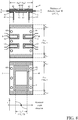
- FIG. 3 illustrates a structure of a waveguide/transmission line converter according to a first embodiment.
- An uppermost stage illustrates a side-sectional view of a waveguide/transmission line converter 1.
- a second stage illustrates a plan-sectional view taken along an arrow A-A of the waveguide/transmission line converter 1.
- a third stage illustrates a plan-sectional view taken along an arrow B-B of the waveguide/transmission line converter 1.
- a lowest stage illustrates electric field distribution in a resonant length direction of a matching element 17 described later.
- the waveguide/transmission line converter 1 includes a dielectric substrate 13, a short-circuit metal layer 14, a metal member 15, a ground metal layer 16, and the matching element 17.
- the dielectric substrate 13 is arranged in a manner blocking an opening of a waveguide 11.
- a surface of the dielectric substrate 13 is the surface perpendicular to a waveguide direction of the waveguide 11.
- a portion of the dielectric substrate 13 where a pattern is arranged is indicated by a white background, and a portion of the dielectric substrate 13 where no pattern is arranged is indicated by hatching.
- the metal member 15 and the ground metal layer 16, which allow the waveguide 11 to extend inside the dielectric substrate 13 and are adapted to hold the short-circuit metal layer 14 at the potential same as that of the waveguide 11, are made to remain along the cross-sections of the two wide walls of the waveguide 11 and removed along cross-sections of two narrow walls of the waveguide 11 so as to prevent an electromagnetic wave from unintendedly being radiated.
- the matching element 17 is arranged on the surface of the dielectric substrate 13 and inside the waveguide 11 and electromagnetically coupled to the transmission line 12 via the dielectric substrate 13, in which a resonant length (approximately ⁇ g '/2) adapted to set up, as a standing wave, an electromagnetic wave having an effective wavelength ⁇ g ' in a surrounding environment of the dielectric substrate 13 is in an electric field direction inside the waveguide 11 and in a feed power direction of the transmission line 12.
- a resonant length approximately ⁇ g '/2
- the matching element 17 and the transmission line 12 exist in separate layers. Additionally, an end shape of the transmission line 12 is a stub provided with a cut-away portion or a slot. Therefore, the matching element 17 and the transmission line 12 can achieve electromagnetic coupling.
- the metal member 15 is formed as a "through hole” penetrating the dielectric substrate 13 along the cross-sections of the two wide walls of the waveguide 11.
- the metal member 15 may be a "conductor wall” penetrating the dielectric substrate 13 along the cross-sections of the two wide walls of the waveguide 11.
- the metal member 15 may be formed as a "through hole” penetrating the dielectric substrate 13 along the cross-sections of the two wide walls and a cross-section of one of two narrow walls of the waveguide 11.
- the metal member 15 may be a "conductor wall” penetrating the dielectric substrate 13 along the cross-sections of the two wide walls and the cross-section of one of the two narrow walls of the waveguide 11.
- only one transmission line 12 is arranged.
- two transmission lines 12 extending in opposite directions may be arranged. However, it is not necessary to arrange two matching elements 17, and arranging only one is enough. Then, the two transmission lines 12 extending in the opposite directions may share one matching element 17.
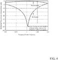
- FIG. 4 illustrates characteristics of the waveguide/transmission line converter according to the first embodiment.
- a low reflection characteristic and a high transmission characteristic can be achieved even in a frequency deviated from a center frequency of the waveguide/transmission line converter 1 by a bandwidth.
- a size p W1 in a direction along the cross-section of the wide wall of the waveguide 11 among the sizes of patterns arranged on the surface of the dielectric substrate 13 can be reduced by a removal width 2n W1 or n W1 (refer to FIG. 3 ) of the metal member 15 and the ground metal layer 16 which have been removed along the cross-sections of both or the cross-section of one of the two narrow walls of the waveguide 11.
- the size p W1 in FIG. 3 is about 2/3 in millimeter wave application in which the size of the metal member 15 cannot be ignored.
- FIGS. 5 and 6 illustrate structures of an antenna device according to the first embodiment.
- the antenna elements are arranged in a lattice shape on a plane.
- the waveguide/transmission line converter 1 is arranged on a straight line in a horizontal direction of the drawing.
- the waveguide/transmission line converter 1 is arranged in a zigzag manner in the horizontal direction of the drawing.
- the antenna elements arranged in a lattice shape are divided per antenna elements 21 in each column.
- the antenna elements 21 in each column are power supplied from two transmission lines 12 which are connected to the waveguide/transmission line converter 1 arranged in a center of each column and extend in opposite directions (described as the modified example two paragraphs before).
- the dielectric substrate 13 is a plane on which the antenna elements are arranged in a lattice shape.
- the cross-section of the wide wall of the waveguide 11 is arranged in a direction perpendicular to a direction of each column.
- the cross-section of the narrow wall of the waveguide 11 is arranged in a direction parallel to the direction of each column.
- the antenna elements 21 in each column have power supplied in the center of each column, a result of synthesizing the respective antenna elements constituting each column can form a directivity having high gain in one arbitrary direction in a wide frequency range even when excitation phases of the respective antenna elements constituting each column are deviated from each other at a frequency deviated from a center frequency of the antenna device 2.
- the size p W1 (refer to FIG. 3 ) in the direction along the cross-section of the wide wall of the waveguide 11 among the sizes of the patterns arranged on the surface of the dielectric substrate 13 can be reduced by a removal width 2n W1 or n W1 (refer to FIG. 3 ) of the metal member 15 and the ground metal layer 16 which have been removed along the cross-sections of both or the cross-section of one of the two narrow walls of the waveguide 11.
- the size p W1 in FIG. 3 is about 2/3 in millimeter wave application in which the size of the metal member 15 cannot be ignored.
- a distance d 1 between the antenna elements 21 in the respective columns adjacent to each other can be made narrower than a length ⁇ 0 /2 that is equal to half a wavelength ⁇ 0 of a radiated electromagnetic wave, a visible region in an array antenna can be narrowed, and grating lobe(s) hardly occur(s) in the directivity of the array antenna formed of the respective antenna elements constituting the respective columns, particularly at the time of adjusting phase information of the respective antenna elements and performing beam scanning to a wide field of view.
- FIG. 7 illustrates a structure of a waveguide/transmission line converter according to a second embodiment.
- An uppermost stage illustrates a side-sectional view of a waveguide/transmission line converter 3.
- a second stage illustrates a plan-sectional view taken along an arrow C-C of the waveguide/transmission line converter 3.
- a third stage illustrates a plan-sectional view taken along an arrow D-D of the waveguide/transmission line converter 3.
- a lowest stage illustrates electric field distribution in a resonant length direction of a matching element 37 described later.
- the waveguide/transmission line converter 3 includes a dielectric substrate 33, a short-circuit metal layer 34, a metal member 35, a ground metal layer 36, a matching element 37, and a dielectric layer 30 in order to convert power transmitted by a waveguide 31 and power transmitted by a transmission line 32 to each other.
- the waveguide 31, transmission line 32, dielectric substrate 33, short-circuit metal layer 34, metal member 35, ground metal layer 36, and matching element 37 of the second embodiment in FIG. 7 are substantially similar to a waveguide 11, a transmission line 12, a dielectric substrate 13, a short-circuit metal layer 14, a metal member 15, a ground metal layer 16, and a matching element 17 of a first embodiment in FIG. 3 , respectively.
- the matching element 37 is arranged on a surface of the dielectric substrate 33 and inside the waveguide 31, and electromagnetically coupled to the transmission line 32 via the dielectric substrate 33, in which a resonant length (approximately ⁇ g /2) adapted to set up, as a standing wave, an electromagnetic wave having an effective wavelength ⁇ g (described later together with the dielectric layer 30) in a surrounding environment of the matching element 37 is in an electric field direction inside the waveguide 31 and in a feed power direction of the transmission line 32.
- a resonant length approximately ⁇ g /2
- the dielectric layer 30 is formed in contact with or close to surfaces of the transmission line 32 and of the short-circuit metal layer 34. Therefore, in the second embodiment, compared to the first embodiment, an effective dielectric constant in the surrounding environment of the waveguide/transmission line converter 3 can be increased and the effective wavelength ⁇ g of an electromagnetic wave in the surrounding environment of the waveguide/transmission line converter 3 can be shortened, and sizes p N2 and p W2 in a direction along cross-sections of a narrow wall and a wide wall of the waveguide 31 can be reduced.
- the dielectric layer 30 desirably has a thickness of 0.2 times or less of the effective wavelength ⁇ g of the electromagnetic wave in the surrounding environment of the waveguide/transmission line converter 3. Accordingly, in order to cover a region where an electric field may leak from the dielectric substrate 33 between the transmission line 32 and the matching element 37, the dielectric layer 30 is required to have only a minimal thickness. Additionally, even when the dielectric layer 30 having the minimal thickness (0.2 times or less of ⁇ g ) is formed in millimeter wave application in which a thickness (about 0.5 mm or less) of the dielectric substrate 33 is reduced, strength of the waveguide/transmission line converter 3 can be increased, and a size of the waveguide/transmission line converter 3 can be reduced. In the description for FIG. 7 , the dielectric layer 30 is formed only on the surfaces of the transmission line 32 and the short-circuit metal layer 34. As a modified example of FIG. 7 , the dielectric layer 30 may be formed on an entire surface of the dielectric substrate 33.
- FIG. 8 illustrates a structure of a waveguide/transmission line converter according to a third embodiment.
- An uppermost stage illustrates a side-sectional view of a waveguide/transmission line converter 4.
- a second stage illustrates a plan-sectional view taken along an arrow E-E of the waveguide/transmission line converter 4.
- a third stage illustrates a plan-sectional view taken along an arrow F-F of the waveguide/transmission line converter 4.
- a lowest stage illustrates electric field distribution in a resonant length direction of a matching element 47 described later.
- the waveguide/transmission line converter 4 includes a dielectric substrate 43, a short-circuit metal layer 44, a metal member 45, a ground metal layer 46, a matching element 47, and a dielectric layer 40 in order to convert power transmitted by a waveguide 41 and power transmitted by a transmission line 42 to each other.
- the waveguide 41, transmission line 42, dielectric substrate 43, short-circuit metal layer 44, metal member 45, ground metal layer 46, matching element 47, dielectric layer 40, sizes p N3 and p W3 , and an effective wavelength ⁇ g of the third embodiment in FIG. 8 are substantially similar to a waveguide 31, a transmission line 32, a dielectric substrate 33, a short-circuit metal layer 34, a metal member 35, a ground metal layer 36, a matching element 37, a dielectric layer 30, sizes p N2 and p W2 , and an effective wavelength ⁇ g of the second embodiment in FIG. 7 , respectively.
- two pairs of transmission lines 42 extend in opposite directions away from the waveguide/transmission line converter 4 along a resonant length direction of the matching element 47.
- a plurality of transmission lines 42 may extend in one direction while a single or a plurality of transmission lines 42 may extend in another direction, out of the two directions away from the waveguide/transmission line converter 4 along the resonant length direction of the matching element 47.
- antennas can be arrayed in a direction perpendicular to a feed power direction only with one waveguide/transmission line converter 4, and high degree of freedom is provided to performance of an array antenna.
- FIGS. 9 and 10 illustrate structures of an antenna device according to the third embodiment.
- antenna elements are arranged in a lattice shape on a plane.
- the waveguide/transmission line converter 4 is arranged on a straight line in a horizontal direction of the drawing.
- the waveguide/transmission line converter 4 is arranged in a zigzag manner in the horizontal direction of the drawing.
- the antenna elements arranged in a lattice shape are divided per antenna elements 51 in every two columns.
- the antenna elements 51 in every two columns are power supplied from each two transmission lines 42 which are connected to the waveguide/transmission line converter 4 arranged in a center of every two columns and respectively extend in opposite directions (described in FIG. 8 as the third embodiment).
- the dielectric substrate 43 is a plane on which the antenna elements are arranged in a lattice shape.
- a cross-section of a wide wall of the waveguide 41 is arranged in a direction perpendicular to a direction of every two columns.
- a cross-section of a narrow wall of the waveguide 41 is arranged in a direction parallel to the direction of every two columns.
- the size p W3 (refer to FIG. 8 ) in a direction along the cross-section of the wide wall of the waveguide 41 among the sizes of patterns arranged on the surface of the dielectric substrate 43 can be reduced by a removal width 2n W3 or n W3 (refer to FIG. 8 ) of the metal member 45 and the ground metal layer 46 which have been removed along cross-sections of both or a cross-section of one of the two narrow walls of the waveguide 41.
- the size p W3 in FIG. 8 is about 2/3 in millimeter wave application in which a size of the metal member 45 cannot be ignored. Therefore, in the antenna device 5, a distance d 3 between the antenna elements in the respective columns adjacent to each other can be made narrower than a length ⁇ 0 /2 that is equal to half a wavelength ⁇ 0 of a radiated electromagnetic wave.
- the waveguide/transmission line converter and the antenna device according to the present disclosure are applicable for a purpose to downsize, at low cost, an antenna device in which a result of synthesis can form directivity having high gain in one arbitrary direction in a wide frequency range, grating lobe(s) hardly occur(s), and antenna elements are arranged in a lattice on a plane.
Landscapes
- Variable-Direction Aerials And Aerial Arrays (AREA)
- Waveguide Aerials (AREA)
Claims (5)
- Un convertisseur de guide d'ondes/ligne de transmission (1, 3, 4) configuré pour convertir la puissance transmise par un guide d'ondes (11, 31, 41) et la puissance transmise par une ligne de transmission (12, 32, 42) l'un à l'autre, le convertisseur de guide d'ondes/ligne de transmission (12, 32, 42) comprenant:un substrat diélectrique (13, 33, 43) agencé de manière à bloquer une ouverture du guide d'ondes (11, 31, 41);une couche métallique court-circuit (14, 34, 44) agencée sur une surface du substrat diélectrique (13, 33, 43) ainsi qu' à l'extérieur du guide d'ondes (11, 31, 41) et maintenue à un potentiel identique à un potentiel des parois du guide d'ondes (11, 31, 41),- par un élément métallique (15, 35, 45) pénétrant le substrat diélectrique (13, 33, 43) le long de sections transversales de deux parois larges du guide d'ondes (11, 31, 41) et non le long de sections transversales de deux parois étroites du guide d'ondes (11, 31, 41); ou- par un élément métallique (15, 35, 45) pénétrant le substrat diélectrique (13, 33, 43) le long de sections transversales des deux parois larges et d'une section transversale de l'une des deux parois étroites du guide d'ondes et non le long d'une section transversale de l'autre des deux parois étroites du guide d'ondes (11, 31, 41); etun élément d'adaptation (17, 37, 47) agencé sur une surface du substrat diélectrique (13, 33, 43) ainsi qu'à l'intérieur du guide d'ondes (11, 31, 41), couplé à la ligne de transmission (12, 32, 42) et ayant une longueur de résonnance dans la direction d'un champ électrique à l'intérieur du guide d'ondes (11, 31, 41) ainsi que dans la direction de l'alimentation en puissance de la ligne de transmission (12, 32, 42),où la longueur de résonance est adaptée de façon à mettre en place, comme onde stationnaire, une onde électromagnétique ayant une longueur d'onde effective dans un milieu environnant du substrat diélectrique (13, 33. 43); etla ligne de transmission (12, 32, 42) étant couplée électro-magnétiquement à l'élément d'adaptation (17, 37, 47) via le substrat diélectrique (13, 33, 43), où une forme de l'extrémité de la ligne de transmission (12, 32, 42) est un embout muni d'une partie découpée ou d'une fente.
- Le convertisseur de guide d'ondes/ligne de transmission (3, 4) selon la première revendication, comprenant en outre une couche diélectrique (30, 40) formée sur des surfaces de la ligne de transmission (32, 42) et de la couche métallique court-circuit (34, 44).
- Le convertisseur de guide d'ondes/ligne de transmission (3, 4) selon la revendication 2, où la couche diélectrique (30, 40) a une épaisseur égale ou inférieure à 0,2 fois la longueur d'onde effective d'une onde électromagnétique dans le milieu environnant du convertisseur de guide d'ondes/ligne de transmission (3, 4).
- Le convertisseur de guide d'ondes/ligne de transmission (1, 3, 4) selon l'une quelconque des revendications 1 à 3, où une pluralité des lignes de transmission (12, 32, 42) comprenant ladite ligne de transmission s'étend dans au moins l'un des deux sens s'éloignant du convertisseur de guide d'ondes/ligne de transmission (1, 3, 4) le long de la direction de la longueur de résonance de l'élément d'adaptation (17, 37, 47) .
- Un dispositif d'antenne (2, 5) ayant des éléments d'antenne agencés sous forme de réseau sur un plan,
où les éléments d'antenne agencés sous forme de réseau sont divisés par des éléments d'antenne agencés dans chaque colonne (21, 51),
où chaque colonne est reliée à un convertisseur de guide d'ondes/lignes de transmission correspondant selon l'une quelconque des revendications 1 à 4, respectivement,
où le dispositif d'antenne est configuré de telle sorte que la puissance soit fournie par la ligne de transmission (12, 32, 42) du convertisseur de guide d'ondes/ligne de transmission (1, 3, 4) aux éléments d'antenne agencés dans chaque colonne (21, 51),
le substrat diélectrique (13, 33, 43) est un plan sur lequel les éléments d'antenne sont agencés sous forme de réseau,
une section transversale d'une paroi large du guide d'ondes (11, 31, 41) est agencée dans une direction perpendiculaire à chaque colonne, et
une section transversale d'une paroi étroite du guide d'ondes (11, 31, 41) est agencée dans une direction parallèle à chaque colonne.
Applications Claiming Priority (3)
| Application Number | Priority Date | Filing Date | Title |
|---|---|---|---|
| JP2015058860 | 2015-03-23 | ||
| JP2016016965A JP6721352B2 (ja) | 2015-03-23 | 2016-02-01 | 導波管/伝送線路変換器及びアンテナ装置 |
| PCT/JP2016/058847 WO2016152811A1 (fr) | 2015-03-23 | 2016-03-18 | Convertisseur de tube de guide d'ondes/ligne de transmission et dispositif d'antenne |
Publications (3)
| Publication Number | Publication Date |
|---|---|
| EP3276741A1 EP3276741A1 (fr) | 2018-01-31 |
| EP3276741A4 EP3276741A4 (fr) | 2018-11-21 |
| EP3276741B1 true EP3276741B1 (fr) | 2021-02-17 |
Family
ID=57132831
Family Applications (1)
| Application Number | Title | Priority Date | Filing Date |
|---|---|---|---|
| EP16768714.4A Active EP3276741B1 (fr) | 2015-03-23 | 2016-03-18 | Convertisseur de tube de guide d'ondes/ligne de transmission et dispositif d'antenne |
Country Status (4)
| Country | Link |
|---|---|
| US (1) | US10483611B2 (fr) |
| EP (1) | EP3276741B1 (fr) |
| JP (1) | JP6721352B2 (fr) |
| CN (1) | CN107408749B (fr) |
Families Citing this family (2)
| Publication number | Priority date | Publication date | Assignee | Title |
|---|---|---|---|---|
| US11404758B2 (en) * | 2018-05-04 | 2022-08-02 | Whirlpool Corporation | In line e-probe waveguide transition |
| EP4352822A4 (fr) | 2021-12-02 | 2024-10-23 | Samsung Electronics Co., Ltd. | Antenne intégrée de carte de circuit imprimé pour émettre/recevoir des données |
Family Cites Families (11)
| Publication number | Priority date | Publication date | Assignee | Title |
|---|---|---|---|---|
| US4603332A (en) * | 1984-09-14 | 1986-07-29 | The Singer Company | Interleaved microstrip planar array |
| US6580335B1 (en) * | 1998-12-24 | 2003-06-17 | Kabushiki Kaisha Toyota Chuo Kenkyusho | Waveguide-transmission line transition having a slit and a matching element |
| JP3317293B2 (ja) * | 1998-12-24 | 2002-08-26 | 株式会社豊田中央研究所 | 導波管・伝送線路変換器 |
| US6822528B2 (en) * | 2001-10-11 | 2004-11-23 | Fujitsu Limited | Transmission line to waveguide transition including antenna patch and ground ring |
| DE10350346B4 (de) * | 2002-10-29 | 2012-12-20 | Kyocera Corp. | Hochfrequenzleitungs-Wellenleiter-Konverter und Hochfrequenzpaket |
| JP2004320460A (ja) | 2003-04-16 | 2004-11-11 | New Japan Radio Co Ltd | マイクロストリップ線路−導波管変換器およびその製造方法 |
| JP2005079733A (ja) | 2003-08-29 | 2005-03-24 | New Japan Radio Co Ltd | 導波管−マイクロストリップ線路分配器 |
| JP2005260570A (ja) * | 2004-03-11 | 2005-09-22 | Mitsubishi Electric Corp | マイクロストリップ線路導波管変換器 |
| JP5387133B2 (ja) * | 2009-05-20 | 2014-01-15 | 日本電気株式会社 | 半導体装置 |
| JP6318392B2 (ja) * | 2013-06-18 | 2018-05-09 | 日本無線株式会社 | 2ポートトリプレート線路−導波管変換器 |
| JP5840736B2 (ja) * | 2014-06-11 | 2016-01-06 | 日本ピラー工業株式会社 | 平面アンテナ |
-
2016
- 2016-02-01 JP JP2016016965A patent/JP6721352B2/ja active Active
- 2016-03-18 US US15/560,396 patent/US10483611B2/en active Active
- 2016-03-18 CN CN201680016997.7A patent/CN107408749B/zh active Active
- 2016-03-18 EP EP16768714.4A patent/EP3276741B1/fr active Active
Non-Patent Citations (1)
| Title |
|---|
| None * |
Also Published As
| Publication number | Publication date |
|---|---|
| JP2016181895A (ja) | 2016-10-13 |
| JP6721352B2 (ja) | 2020-07-15 |
| CN107408749B (zh) | 2020-02-11 |
| EP3276741A1 (fr) | 2018-01-31 |
| US10483611B2 (en) | 2019-11-19 |
| US20180069286A1 (en) | 2018-03-08 |
| CN107408749A (zh) | 2017-11-28 |
| EP3276741A4 (fr) | 2018-11-21 |
Similar Documents
| Publication | Publication Date | Title |
|---|---|---|
| JP6386182B2 (ja) | 導波管スロットアレイアンテナ | |
| JP6395984B2 (ja) | アレーアンテナ装置 | |
| US9692117B2 (en) | Antenna | |
| JPWO2017150054A1 (ja) | アレーアンテナ | |
| US20160079674A1 (en) | Distributor And Planar Antenna | |
| EP2337153B1 (fr) | Antenne réseau à fentes et appareil radar | |
| WO2010098191A1 (fr) | Convertisseur de ligne microruban-guide d'ondes | |
| US10873121B2 (en) | Antenna device | |
| EP3780279A1 (fr) | Appareil d'antenne réseau et dispositif de communication | |
| EP3331092B1 (fr) | Circuit d'alimentation | |
| EP3276741B1 (fr) | Convertisseur de tube de guide d'ondes/ligne de transmission et dispositif d'antenne | |
| JP6474634B2 (ja) | 平面アレーアンテナ | |
| JP6611238B2 (ja) | 導波管/伝送線路変換器、アレーアンテナ及び平面アンテナ | |
| JP2013034118A (ja) | アレーアンテナ | |
| JP2008167246A (ja) | 導波管アレーアンテナ | |
| JP6613156B2 (ja) | 導波管/伝送線路変換器及びアンテナ装置 | |
| JP2011199499A (ja) | アンテナ装置およびアレーアンテナ装置 | |
| JP5377070B2 (ja) | 導波管/マイクロストリップ線路変換器 | |
| JP6613157B2 (ja) | 導波管/伝送線路変換器、アンテナ装置、及び、導波管/伝送線路変換器を製造する方法 | |
| EP3429024A1 (fr) | Circuit déphaseur et circuit d'alimentation électrique | |
| WO2016152811A1 (fr) | Convertisseur de tube de guide d'ondes/ligne de transmission et dispositif d'antenne | |
| JP2023131594A (ja) | アンテナ装置 | |
| JP6313812B2 (ja) | 給電装置 | |
| Chan | Broadband dual polarized end-launched coaxial transition for dielectric-filled square waveguide | |
| Hernandez et al. | Design of V-band substrate integrated waveguide fed aperture coupled microstrip patch array with beam-switching capabilities |
Legal Events
| Date | Code | Title | Description |
|---|---|---|---|
| STAA | Information on the status of an ep patent application or granted ep patent |
Free format text: STATUS: THE INTERNATIONAL PUBLICATION HAS BEEN MADE |
|
| PUAI | Public reference made under article 153(3) epc to a published international application that has entered the european phase |
Free format text: ORIGINAL CODE: 0009012 |
|
| STAA | Information on the status of an ep patent application or granted ep patent |
Free format text: STATUS: REQUEST FOR EXAMINATION WAS MADE |
|
| 17P | Request for examination filed |
Effective date: 20171023 |
|
| AK | Designated contracting states |
Kind code of ref document: A1 Designated state(s): AL AT BE BG CH CY CZ DE DK EE ES FI FR GB GR HR HU IE IS IT LI LT LU LV MC MK MT NL NO PL PT RO RS SE SI SK SM TR |
|
| AX | Request for extension of the european patent |
Extension state: BA ME |
|
| DAV | Request for validation of the european patent (deleted) | ||
| DAX | Request for extension of the european patent (deleted) | ||
| A4 | Supplementary search report drawn up and despatched |
Effective date: 20181024 |
|
| RIC1 | Information provided on ipc code assigned before grant |
Ipc: H01Q 13/08 20060101ALI20181017BHEP Ipc: H01Q 21/00 20060101ALI20181017BHEP Ipc: H01P 5/107 20060101AFI20181017BHEP Ipc: H01Q 21/06 20060101ALI20181017BHEP |
|
| STAA | Information on the status of an ep patent application or granted ep patent |
Free format text: STATUS: EXAMINATION IS IN PROGRESS |
|
| 17Q | First examination report despatched |
Effective date: 20191104 |
|
| GRAP | Despatch of communication of intention to grant a patent |
Free format text: ORIGINAL CODE: EPIDOSNIGR1 |
|
| STAA | Information on the status of an ep patent application or granted ep patent |
Free format text: STATUS: GRANT OF PATENT IS INTENDED |
|
| INTG | Intention to grant announced |
Effective date: 20200326 |
|
| RAP1 | Party data changed (applicant data changed or rights of an application transferred) |
Owner name: JAPAN RADIO CO., LTD. |
|
| GRAJ | Information related to disapproval of communication of intention to grant by the applicant or resumption of examination proceedings by the epo deleted |
Free format text: ORIGINAL CODE: EPIDOSDIGR1 |
|
| STAA | Information on the status of an ep patent application or granted ep patent |
Free format text: STATUS: EXAMINATION IS IN PROGRESS |
|
| INTC | Intention to grant announced (deleted) | ||
| GRAP | Despatch of communication of intention to grant a patent |
Free format text: ORIGINAL CODE: EPIDOSNIGR1 |
|
| STAA | Information on the status of an ep patent application or granted ep patent |
Free format text: STATUS: GRANT OF PATENT IS INTENDED |
|
| INTG | Intention to grant announced |
Effective date: 20200918 |
|
| GRAS | Grant fee paid |
Free format text: ORIGINAL CODE: EPIDOSNIGR3 |
|
| GRAA | (expected) grant |
Free format text: ORIGINAL CODE: 0009210 |
|
| STAA | Information on the status of an ep patent application or granted ep patent |
Free format text: STATUS: THE PATENT HAS BEEN GRANTED |
|
| AK | Designated contracting states |
Kind code of ref document: B1 Designated state(s): AL AT BE BG CH CY CZ DE DK EE ES FI FR GB GR HR HU IE IS IT LI LT LU LV MC MK MT NL NO PL PT RO RS SE SI SK SM TR |
|
| REG | Reference to a national code |
Ref country code: GB Ref legal event code: FG4D |
|
| REG | Reference to a national code |
Ref country code: CH Ref legal event code: EP |
|
| REG | Reference to a national code |
Ref country code: DE Ref legal event code: R096 Ref document number: 602016052626 Country of ref document: DE |
|
| REG | Reference to a national code |
Ref country code: AT Ref legal event code: REF Ref document number: 1362687 Country of ref document: AT Kind code of ref document: T Effective date: 20210315 |
|
| REG | Reference to a national code |
Ref country code: IE Ref legal event code: FG4D |
|
| REG | Reference to a national code |
Ref country code: LT Ref legal event code: MG9D |
|
| REG | Reference to a national code |
Ref country code: NL Ref legal event code: MP Effective date: 20210217 |
|
| PG25 | Lapsed in a contracting state [announced via postgrant information from national office to epo] |
Ref country code: FI Free format text: LAPSE BECAUSE OF FAILURE TO SUBMIT A TRANSLATION OF THE DESCRIPTION OR TO PAY THE FEE WITHIN THE PRESCRIBED TIME-LIMIT Effective date: 20210217 Ref country code: GR Free format text: LAPSE BECAUSE OF FAILURE TO SUBMIT A TRANSLATION OF THE DESCRIPTION OR TO PAY THE FEE WITHIN THE PRESCRIBED TIME-LIMIT Effective date: 20210518 Ref country code: HR Free format text: LAPSE BECAUSE OF FAILURE TO SUBMIT A TRANSLATION OF THE DESCRIPTION OR TO PAY THE FEE WITHIN THE PRESCRIBED TIME-LIMIT Effective date: 20210217 Ref country code: NO Free format text: LAPSE BECAUSE OF FAILURE TO SUBMIT A TRANSLATION OF THE DESCRIPTION OR TO PAY THE FEE WITHIN THE PRESCRIBED TIME-LIMIT Effective date: 20210517 Ref country code: PT Free format text: LAPSE BECAUSE OF FAILURE TO SUBMIT A TRANSLATION OF THE DESCRIPTION OR TO PAY THE FEE WITHIN THE PRESCRIBED TIME-LIMIT Effective date: 20210617 Ref country code: BG Free format text: LAPSE BECAUSE OF FAILURE TO SUBMIT A TRANSLATION OF THE DESCRIPTION OR TO PAY THE FEE WITHIN THE PRESCRIBED TIME-LIMIT Effective date: 20210517 Ref country code: LT Free format text: LAPSE BECAUSE OF FAILURE TO SUBMIT A TRANSLATION OF THE DESCRIPTION OR TO PAY THE FEE WITHIN THE PRESCRIBED TIME-LIMIT Effective date: 20210217 |
|
| REG | Reference to a national code |
Ref country code: AT Ref legal event code: MK05 Ref document number: 1362687 Country of ref document: AT Kind code of ref document: T Effective date: 20210217 |
|
| PG25 | Lapsed in a contracting state [announced via postgrant information from national office to epo] |
Ref country code: NL Free format text: LAPSE BECAUSE OF FAILURE TO SUBMIT A TRANSLATION OF THE DESCRIPTION OR TO PAY THE FEE WITHIN THE PRESCRIBED TIME-LIMIT Effective date: 20210217 Ref country code: PL Free format text: LAPSE BECAUSE OF FAILURE TO SUBMIT A TRANSLATION OF THE DESCRIPTION OR TO PAY THE FEE WITHIN THE PRESCRIBED TIME-LIMIT Effective date: 20210217 Ref country code: RS Free format text: LAPSE BECAUSE OF FAILURE TO SUBMIT A TRANSLATION OF THE DESCRIPTION OR TO PAY THE FEE WITHIN THE PRESCRIBED TIME-LIMIT Effective date: 20210217 Ref country code: LV Free format text: LAPSE BECAUSE OF FAILURE TO SUBMIT A TRANSLATION OF THE DESCRIPTION OR TO PAY THE FEE WITHIN THE PRESCRIBED TIME-LIMIT Effective date: 20210217 Ref country code: SE Free format text: LAPSE BECAUSE OF FAILURE TO SUBMIT A TRANSLATION OF THE DESCRIPTION OR TO PAY THE FEE WITHIN THE PRESCRIBED TIME-LIMIT Effective date: 20210217 |
|
| PG25 | Lapsed in a contracting state [announced via postgrant information from national office to epo] |
Ref country code: IS Free format text: LAPSE BECAUSE OF FAILURE TO SUBMIT A TRANSLATION OF THE DESCRIPTION OR TO PAY THE FEE WITHIN THE PRESCRIBED TIME-LIMIT Effective date: 20210617 |
|
| PG25 | Lapsed in a contracting state [announced via postgrant information from national office to epo] |
Ref country code: CZ Free format text: LAPSE BECAUSE OF FAILURE TO SUBMIT A TRANSLATION OF THE DESCRIPTION OR TO PAY THE FEE WITHIN THE PRESCRIBED TIME-LIMIT Effective date: 20210217 Ref country code: EE Free format text: LAPSE BECAUSE OF FAILURE TO SUBMIT A TRANSLATION OF THE DESCRIPTION OR TO PAY THE FEE WITHIN THE PRESCRIBED TIME-LIMIT Effective date: 20210217 Ref country code: SM Free format text: LAPSE BECAUSE OF FAILURE TO SUBMIT A TRANSLATION OF THE DESCRIPTION OR TO PAY THE FEE WITHIN THE PRESCRIBED TIME-LIMIT Effective date: 20210217 Ref country code: AT Free format text: LAPSE BECAUSE OF FAILURE TO SUBMIT A TRANSLATION OF THE DESCRIPTION OR TO PAY THE FEE WITHIN THE PRESCRIBED TIME-LIMIT Effective date: 20210217 |
|
| REG | Reference to a national code |
Ref country code: CH Ref legal event code: PL |
|
| REG | Reference to a national code |
Ref country code: DE Ref legal event code: R097 Ref document number: 602016052626 Country of ref document: DE |
|
| PG25 | Lapsed in a contracting state [announced via postgrant information from national office to epo] |
Ref country code: SK Free format text: LAPSE BECAUSE OF FAILURE TO SUBMIT A TRANSLATION OF THE DESCRIPTION OR TO PAY THE FEE WITHIN THE PRESCRIBED TIME-LIMIT Effective date: 20210217 Ref country code: RO Free format text: LAPSE BECAUSE OF FAILURE TO SUBMIT A TRANSLATION OF THE DESCRIPTION OR TO PAY THE FEE WITHIN THE PRESCRIBED TIME-LIMIT Effective date: 20210217 Ref country code: DK Free format text: LAPSE BECAUSE OF FAILURE TO SUBMIT A TRANSLATION OF THE DESCRIPTION OR TO PAY THE FEE WITHIN THE PRESCRIBED TIME-LIMIT Effective date: 20210217 Ref country code: MC Free format text: LAPSE BECAUSE OF FAILURE TO SUBMIT A TRANSLATION OF THE DESCRIPTION OR TO PAY THE FEE WITHIN THE PRESCRIBED TIME-LIMIT Effective date: 20210217 |
|
| REG | Reference to a national code |
Ref country code: BE Ref legal event code: MM Effective date: 20210331 |
|
| PLBE | No opposition filed within time limit |
Free format text: ORIGINAL CODE: 0009261 |
|
| STAA | Information on the status of an ep patent application or granted ep patent |
Free format text: STATUS: NO OPPOSITION FILED WITHIN TIME LIMIT |
|
| 26N | No opposition filed |
Effective date: 20211118 |
|
| PG25 | Lapsed in a contracting state [announced via postgrant information from national office to epo] |
Ref country code: ES Free format text: LAPSE BECAUSE OF FAILURE TO SUBMIT A TRANSLATION OF THE DESCRIPTION OR TO PAY THE FEE WITHIN THE PRESCRIBED TIME-LIMIT Effective date: 20210217 Ref country code: IE Free format text: LAPSE BECAUSE OF NON-PAYMENT OF DUE FEES Effective date: 20210318 Ref country code: CH Free format text: LAPSE BECAUSE OF NON-PAYMENT OF DUE FEES Effective date: 20210331 Ref country code: AL Free format text: LAPSE BECAUSE OF FAILURE TO SUBMIT A TRANSLATION OF THE DESCRIPTION OR TO PAY THE FEE WITHIN THE PRESCRIBED TIME-LIMIT Effective date: 20210217 Ref country code: LI Free format text: LAPSE BECAUSE OF NON-PAYMENT OF DUE FEES Effective date: 20210331 Ref country code: LU Free format text: LAPSE BECAUSE OF NON-PAYMENT OF DUE FEES Effective date: 20210318 |
|
| PG25 | Lapsed in a contracting state [announced via postgrant information from national office to epo] |
Ref country code: SI Free format text: LAPSE BECAUSE OF FAILURE TO SUBMIT A TRANSLATION OF THE DESCRIPTION OR TO PAY THE FEE WITHIN THE PRESCRIBED TIME-LIMIT Effective date: 20210217 |
|
| PG25 | Lapsed in a contracting state [announced via postgrant information from national office to epo] |
Ref country code: IT Free format text: LAPSE BECAUSE OF FAILURE TO SUBMIT A TRANSLATION OF THE DESCRIPTION OR TO PAY THE FEE WITHIN THE PRESCRIBED TIME-LIMIT Effective date: 20210217 |
|
| PG25 | Lapsed in a contracting state [announced via postgrant information from national office to epo] |
Ref country code: IS Free format text: LAPSE BECAUSE OF FAILURE TO SUBMIT A TRANSLATION OF THE DESCRIPTION OR TO PAY THE FEE WITHIN THE PRESCRIBED TIME-LIMIT Effective date: 20210617 |
|
| PG25 | Lapsed in a contracting state [announced via postgrant information from national office to epo] |
Ref country code: BE Free format text: LAPSE BECAUSE OF NON-PAYMENT OF DUE FEES Effective date: 20210331 |
|
| PG25 | Lapsed in a contracting state [announced via postgrant information from national office to epo] |
Ref country code: CY Free format text: LAPSE BECAUSE OF FAILURE TO SUBMIT A TRANSLATION OF THE DESCRIPTION OR TO PAY THE FEE WITHIN THE PRESCRIBED TIME-LIMIT Effective date: 20210217 |
|
| PG25 | Lapsed in a contracting state [announced via postgrant information from national office to epo] |
Ref country code: HU Free format text: LAPSE BECAUSE OF FAILURE TO SUBMIT A TRANSLATION OF THE DESCRIPTION OR TO PAY THE FEE WITHIN THE PRESCRIBED TIME-LIMIT; INVALID AB INITIO Effective date: 20160318 |
|
| PG25 | Lapsed in a contracting state [announced via postgrant information from national office to epo] |
Ref country code: MK Free format text: LAPSE BECAUSE OF FAILURE TO SUBMIT A TRANSLATION OF THE DESCRIPTION OR TO PAY THE FEE WITHIN THE PRESCRIBED TIME-LIMIT Effective date: 20210217 |
|
| PG25 | Lapsed in a contracting state [announced via postgrant information from national office to epo] |
Ref country code: MT Free format text: LAPSE BECAUSE OF FAILURE TO SUBMIT A TRANSLATION OF THE DESCRIPTION OR TO PAY THE FEE WITHIN THE PRESCRIBED TIME-LIMIT Effective date: 20210217 |
|
| PG25 | Lapsed in a contracting state [announced via postgrant information from national office to epo] |
Ref country code: TR Free format text: LAPSE BECAUSE OF FAILURE TO SUBMIT A TRANSLATION OF THE DESCRIPTION OR TO PAY THE FEE WITHIN THE PRESCRIBED TIME-LIMIT Effective date: 20210217 |
|
| PGFP | Annual fee paid to national office [announced via postgrant information from national office to epo] |
Ref country code: GB Payment date: 20260331 Year of fee payment: 11 |
|
| PGFP | Annual fee paid to national office [announced via postgrant information from national office to epo] |
Ref country code: DE Payment date: 20260331 Year of fee payment: 11 |
|
| PGFP | Annual fee paid to national office [announced via postgrant information from national office to epo] |
Ref country code: FR Payment date: 20260331 Year of fee payment: 11 |