WO2016152811A1 - Convertisseur de tube de guide d'ondes/ligne de transmission et dispositif d'antenne - Google Patents
Convertisseur de tube de guide d'ondes/ligne de transmission et dispositif d'antenne Download PDFInfo
- Publication number
- WO2016152811A1 WO2016152811A1 PCT/JP2016/058847 JP2016058847W WO2016152811A1 WO 2016152811 A1 WO2016152811 A1 WO 2016152811A1 JP 2016058847 W JP2016058847 W JP 2016058847W WO 2016152811 A1 WO2016152811 A1 WO 2016152811A1
- Authority
- WO
- WIPO (PCT)
- Prior art keywords
- waveguide
- transmission line
- dielectric substrate
- line converter
- antenna elements
- Prior art date
- Legal status (The legal status is an assumption and is not a legal conclusion. Google has not performed a legal analysis and makes no representation as to the accuracy of the status listed.)
- Ceased
Links
Images


Classifications
-
- H—ELECTRICITY
- H01—ELECTRIC ELEMENTS
- H01P—WAVEGUIDES; RESONATORS, LINES, OR OTHER DEVICES OF THE WAVEGUIDE TYPE
- H01P5/00—Coupling devices of the waveguide type
- H01P5/08—Coupling devices of the waveguide type for linking dissimilar lines or devices
- H01P5/10—Coupling devices of the waveguide type for linking dissimilar lines or devices for coupling balanced lines or devices with unbalanced lines or devices
- H01P5/107—Hollow-waveguide/strip-line transitions
-
- H—ELECTRICITY
- H01—ELECTRIC ELEMENTS
- H01Q—ANTENNAS, i.e. RADIO AERIALS
- H01Q13/00—Waveguide horns or mouths; Slot antennas; Leaky-waveguide antennas; Equivalent structures causing radiation along the transmission path of a guided wave
- H01Q13/08—Radiating ends of two-conductor microwave transmission lines, e.g. of coaxial lines, of microstrip lines
-
- H—ELECTRICITY
- H01—ELECTRIC ELEMENTS
- H01Q—ANTENNAS, i.e. RADIO AERIALS
- H01Q21/00—Antenna arrays or systems
- H01Q21/06—Arrays of individually energised antenna units similarly polarised and spaced apart
Definitions
- the present disclosure includes: (1) a waveguide / transmission line converter that mutually converts power transmitted by a waveguide and power transmitted by a transmission line; and (2) an antenna element on a plane.
- the present invention relates to an antenna device which is arranged in a grid pattern and is fed by a waveguide / transmission line converter.
- the waveguide / transmission line converter is applied to power feeding to the antenna device and is disclosed in Patent Documents 1 and 2 and the like.
- a transmission line is inserted at a position where the electric field strength is high in the waveguide.
- a waveguide short-circuit surface is required at a position that is separated from the transmission line along the waveguide by a distance equal to approximately 1 ⁇ 4 of the wavelength of the electromagnetic wave in the waveguide. Therefore, in Patent Document 1, the waveguide / transmission line converter cannot be reduced in size, and the structure that forms the short-circuited surface exists in front of the surface that forms the antenna device. Cause deterioration of sex.
- Patent Document 2 a technique of coupling a transmission line to a matching element and propagating radio waves from the transmission line to a waveguide is used.
- the waveguide / transmission line converter can be reduced in size compared to Patent Document 1, and the short-circuit surface that causes the directivity of the antenna device to deteriorate.
- the structure which forms can be eliminated.
- Fig. 1 shows the configuration of a conventional waveguide / transmission line converter.
- the top row shows a side sectional view of the waveguide / transmission line converter 1 '.
- the second stage shows a cross-sectional view of the waveguide / transmission line converter 1 'taken along the arrow A'-A'.
- the third stage shows a cross-sectional plan view of the waveguide / transmission line converter 1 'taken along the arrow B'-B'.
- the bottom row shows the electric field distribution in the direction of the resonance length of the matching element 17 'described later.
- the waveguide / transmission line converter 1 ′ includes a dielectric substrate 13 ′, a short-circuit metal layer 14 ′, a metal member 15 ′, a ground metal layer 16 ′, and a matching element 17 ′.
- the dielectric substrate 13 ′ is disposed so as to close the opening of the waveguide 11 ′.
- the surface of the dielectric substrate 13 ′ is a surface perpendicular to the waveguide direction of the waveguide 11 ′.
- the portion of the dielectric substrate 13 ′ where the pattern is arranged is shown in white, and the portion of the dielectric substrate 13 ′ where the pattern is not arranged is shown in diagonal lines.
- the short-circuit metal layer 14 ' is disposed on the surface of the dielectric substrate 13' and outside the waveguide 11 ', and the metal member 15' penetrating the dielectric substrate 13 'and the surface of the dielectric substrate 13' and the waveguide.
- the ground metal layer 16 'disposed on the outer frame of 11' is held at the same potential as the waveguide 11 '.
- the matching element 17 ′ is disposed on the surface of the dielectric substrate 13 ′ and inside the waveguide 11 ′, and is electromagnetically coupled to the transmission line 12 ′ via the dielectric substrate 13 ′.
- a resonance length (approximately ⁇ g ′ / 2) for standing an electromagnetic wave having an effective wavelength ⁇ g ′ in the surrounding environment as a standing wave is provided in the electric field direction in the waveguide 11 ′ and the feeding direction of the transmission line 12 ′. .
- only one transmission line 12 ' is arranged.
- two transmission lines 12 ′ extending in opposite directions may be arranged.
- the two transmission lines 12 ′ extending in opposite directions may share one matching element 17 ′.
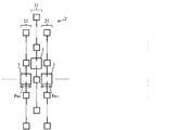
- Fig. 2 shows an example of the configuration of an antenna device using conventional technology.
- the antenna device 2 ′ is not disclosed in Patent Documents 1 and 2.
- antenna elements are arranged in a grid pattern on a plane.
- the antenna elements arranged in a lattice shape are divided into antenna elements 21 'in each column.
- the antenna elements 21 ′ in each row are two transmission lines 12 ′ extending in the opposite direction and connected to a waveguide / transmission line converter 1 ′ disposed in the center of each row (as a modification, one paragraph before Power is supplied as described above).
- the dielectric substrate 13 ' is a plane on which the antenna elements are arranged in a lattice pattern.
- the cross section of the wide wall surface of the waveguide 11 ′ is arranged in a direction perpendicular to the direction of each row.
- the cross section of the narrow wall surface of the waveguide 11 ' is arranged in a direction parallel to the direction of each row.
- the antenna elements 21 'in each column are fed at the center of each column, even if the excitation phases of the antenna elements constituting each column are shifted from each other at a frequency shifted from the center frequency of the antenna device 2', As a result of combining the antenna elements constituting the column, directivity with high gain can be formed in any one direction in a wide frequency range.
- the size p w ′ in the direction along the cross section of the wide wall surface of the waveguide 11 ′ among the sizes of the patterns arranged on the surface of the dielectric substrate 13 ′ (See FIG. 1). Therefore, 'in each column of the antenna elements 21 adjacent to each other' antenna device 2 distance d 'is inevitably wider than the length lambda 0/2 is equal to half the wavelength lambda 0 of the electromagnetic wave having radiated .
- the visible region in the array antenna must be wide, and in the directivity of the array antenna formed by each antenna element constituting each column, in particular, the phase information of each antenna element is adjusted to a wide angle. When scanning the beam, grating lobes in the array antenna are likely to occur.
- the present disclosure provides a waveguide / transmission line converter in a direction along a cross section of a wide wall surface of a waveguide among the sizes of patterns arranged on the surface of a dielectric substrate.
- the interval between the antenna elements adjacent to each other is narrowed, and in the directivity of the array antenna formed by each antenna element constituting each column, in particular, each antenna element It is an object of the present invention to make it difficult to generate a grating lobe when the phase information is adjusted and the beam is scanned to a wide angle.
- a current flowing through a narrow wall surface flows in a direction parallel to the cross section of the narrow wall surface. Applied that electromagnetic waves are not emitted when provided. That is, the metal member for extending the waveguide into the dielectric substrate and holding the short-circuit metal layer at the same potential as the waveguide is left along the cross section of the two wide wall surfaces of the waveguide, Except along the cross section of one of the two surfaces of the waveguide or the narrow wall surface of one surface, the electromagnetic wave is prevented from being inadvertently emitted.
- the present disclosure is a waveguide / transmission line converter that mutually converts power transmitted by a waveguide and power transmitted by a transmission line, A dielectric substrate disposed so as to close the opening; and the dielectric substrate disposed along the surface of the dielectric substrate and outside the waveguide, along a cross section of two wide wall surfaces of the waveguide. Or by a metal member penetrating the dielectric substrate along a cross section of one of the two wide wall surfaces and the two narrow wall surfaces of the waveguide. A short-circuited metal layer held at the same potential as the wave tube, disposed on the surface of the dielectric substrate and inside the waveguide, coupled to the transmission line, and having an effective wavelength in an environment around the dielectric substrate.
- the resonance length for raising an electromagnetic wave as a standing wave is defined as the direction of the electric field in the waveguide.
- a waveguide / transmission line converter characterized in that it comprises a matching element having a feeding direction of the transmission line.
- the size in the direction along the cross section of the wide wall surface of the waveguide can be reduced.
- the present disclosure is a waveguide / transmission line converter further including a dielectric layer formed on a surface of the transmission line and the short-circuit metal layer.
- the effective dielectric constant in the environment around the waveguide / transmission line converter can be increased, and the size of the pattern around the waveguide / transmission line converter can be reduced.
- the thickness of the dielectric layer is 0.2 times or less the effective wavelength of the electromagnetic wave in the environment around the waveguide / transmission line converter. / Transmission line converter.
- a plurality of the transmission lines extend in at least one of the two directions away from the waveguide / transmission line converter along the resonance length direction of the matching element. Is a waveguide / transmission line converter.
- an antenna can be arranged in a direction perpendicular to the feeding direction with only one waveguide / transmission line converter, and a high degree of freedom is imparted to the performance of the array antenna.
- the present disclosure is an antenna device in which antenna elements are arranged in a grid pattern on a plane, and the antenna elements arranged in a grid pattern are divided into antenna elements arranged in each column shape,
- the antenna elements arranged in the antenna are fed by the transmission line connected to the waveguide / transmission line converter arranged in the center of each row, and the antenna elements are arranged in a lattice pattern on the dielectric substrate.
- the cross section of the wide wall surface of the waveguide is arranged in a direction perpendicular to the direction of each row, and the cross section of the narrow wall surface of the waveguide is arranged in a direction parallel to the direction of each row. This is an antenna device.
- the distance between the antenna elements in each column adjacent to each other is narrowed, and in particular, the phase information of each antenna element is adjusted in the directivity of the array antenna formed by each antenna element constituting each column.
- the size along the cross section of the wide wall surface of the waveguide is reduced.
- the distance between the antenna elements in each column adjacent to each other is narrowed, and the phase information of each antenna element is adjusted particularly in the directivity of the array antenna formed by each antenna element constituting each column.
- FIG. 1 The configuration of the waveguide / transmission line converter of the first embodiment is shown in FIG.
- the uppermost stage shows a side sectional view of the waveguide / transmission line converter 1.
- the second stage shows an AA plane cross-sectional view of the waveguide / transmission line converter 1.
- the third stage shows a cross-sectional view taken along the line BB of the waveguide / transmission line converter 1.
- the bottom row shows the electric field distribution in the direction of the resonance length of the matching element 17 described later.
- the waveguide / transmission line converter 1 includes a dielectric substrate 13, a short-circuit metal layer 14, a metal member 15, a ground metal layer 16, and a matching element 17.
- the dielectric substrate 13 is disposed so as to close the opening of the waveguide 11.
- the surface of the dielectric substrate 13 is a surface perpendicular to the waveguide direction of the waveguide 11.
- the portion of the dielectric substrate 13 where the pattern is arranged is shown in white, and the portion of the dielectric substrate 13 where the pattern is not arranged is shown by diagonal lines.
- the short-circuit metal layer 14 is disposed on the surface of the dielectric substrate 13 and outside the waveguide 11, and the metal member 15 penetrating the dielectric substrate 13 along the cross section of the two wide wall surfaces of the waveguide 11 and the dielectric.
- the surface of the body substrate 13 and the ground metal layer 16 disposed on the outer frame of the waveguide 11 are held at the same potential as the waveguide 11. That is, the metal member 15 and the ground metal layer 16 for extending the waveguide 11 into the dielectric substrate 13 and holding the short-circuit metal layer 14 at the same potential as the waveguide 11 are formed on the two surfaces of the waveguide 11. In this case, the electromagnetic wave is not inadvertently radiated except for the cross section of the narrow wall surface of the two surfaces of the waveguide 11.
- the matching element 17 is disposed on the surface of the dielectric substrate 13 and inside the waveguide 11, is electromagnetically coupled to the transmission line 12 via the dielectric substrate 13, and has an effective wavelength in the environment around the dielectric substrate 13.
- a resonance length (approximately ⁇ g ′ / 2) for raising an electromagnetic wave of ⁇ g ′ as a standing wave is provided in the electric field direction in the waveguide 11 and the feeding direction of the transmission line 12.
- the matching element 17 and the transmission line 12 exist in different layers.
- tip shape of the transmission line 12 is a stub or slot with a notch. Therefore, the matching element 17 and the transmission line 12 can realize electromagnetic coupling.
- the metal member 15 is formed as a “through hole” that penetrates the dielectric substrate 13 along the cross section of the two wide wall surfaces of the waveguide 11.
- the metal member 15 may be a “conductor wall” that penetrates the dielectric substrate 13 along the cross section of the two wide wall surfaces of the waveguide 11.
- the metal member 15 penetrates the dielectric substrate 13 along the cross section of the two wide wall surfaces of the waveguide 11 and the narrow wall surface of one of the two surfaces. It may be formed by a “hole”.
- the metal member 15 includes a “conductor” penetrating the dielectric substrate 13 along a cross section of one of the two wide walls and one of the two walls of the waveguide 11. It may be a “wall”.
- only one transmission line 12 is arranged.
- two transmission lines 12 extending in opposite directions may be arranged.
- the two transmission lines 12 extending in the opposite directions may share one matching element 17.
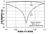
- FIG. 4 shows the characteristics of the waveguide / transmission line converter according to the first embodiment.
- the first embodiment as in the prior art, low reflection characteristics and high transmission characteristics can be realized even at a frequency shifted from the center frequency of the waveguide / transmission line converter 1 by the bandwidth. is there.
- the size p W1 in the direction along the cross section of the wide wall surface of the waveguide 11 out of the sizes of the patterns arranged on the surface of the dielectric substrate 13 as compared with the prior art (see FIG. see 3.) the removal width of the metal member 15 and the grounding metallic layer 16 which has been removed along one or both sides of the narrow walls of the cross section of the two surfaces of the waveguide 11 2n W1 or n W1 (FIG. 3 Can be reduced by the amount of Specifically, the size p W1 in FIG. 3 is about 2/3 in the millimeter wave application in which the dimension of the metal member 15 is not negligible compared to the size p W ′ in FIG.
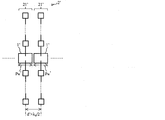
- the antenna elements are arranged in a grid pattern on a plane.
- the waveguide / transmission line converter 1 is arranged on a straight line in the horizontal direction of the drawing.
- the waveguide / transmission line converters 1 are arranged in a staggered manner in the left-right direction of the drawing.
- the antenna elements arranged in a lattice shape are divided into antenna elements 21 in each column.
- the antenna elements 21 in each row are two transmission lines 12 extending in opposite directions connected to the waveguide / transmission line converter 1 disposed in the center of each row (as described in the second paragraph before as a modification). )).
- the dielectric substrate 13 is a plane on which antenna elements are arranged in a lattice pattern.
- the cross section of the wide wall surface of the waveguide 11 is arranged in a direction perpendicular to the direction of each row.
- the section of the narrow wall surface of the waveguide 11 is arranged in a direction parallel to the direction of each row.
- the size p W1 in the direction along the cross section of the wide wall surface of the waveguide 11 among the sizes of the patterns arranged on the surface of the dielectric substrate 13 see FIG. 3). .
- width 2n W1 or n W1 see removed width 2n W1 or n W1 (FIG. 3 of the metal member 15 and the grounding metallic layer 16 which has been removed along the cross-section of the both surfaces or one surface of the narrow walls of the two surfaces of the waveguide 11.
- the size p W1 in FIG. 3 is about 2/3 in the millimeter wave application in which the dimension of the metal member 15 is not negligible compared to the size p W ′ in FIG.
- the antenna device 2 the distance d 1 of each row of antenna elements 21 adjacent to each other may be smaller than half the length equal lambda 0/2 of the wavelength lambda 0 of the electromagnetic wave having radiated, the array antenna In the directivity of the array antenna formed by each antenna element constituting each row, especially when adjusting the phase information of each antenna element and scanning the beam to a wide angle The grating lobe in the array antenna is less likely to occur.
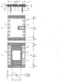
- the configuration of the waveguide / transmission line converter of the second embodiment is shown in FIG.
- the uppermost stage shows a side sectional view of the waveguide / transmission line converter 3.
- the second stage shows a cross-sectional plan view taken along the line CC of the waveguide / transmission line converter 3.
- the third stage shows a cross-sectional view taken along the line DD of the waveguide / transmission line converter 3.
- the bottom row shows the electric field distribution in the direction of the resonance length of the matching element 37 described later.
- the waveguide / transmission line converter 3 includes a dielectric substrate 33, a short-circuit metal layer 34, and the like so as to mutually convert the power transmitted by the waveguide 31 and the power transmitted by the transmission line 32.
- a metal member 35, a ground metal layer 36, a matching element 37, and a dielectric layer 30 are provided.
- the waveguide 31, transmission line 32, dielectric substrate 33, short-circuit metal layer 34, metal member 35, ground metal layer 36 and matching element 37 of the second embodiment in FIG. 7 are the same as those of the first embodiment in FIG.
- the wave tube 11, the transmission line 12, the dielectric substrate 13, the short-circuit metal layer 14, the metal member 15, the ground metal layer 16, and the matching element 17 are substantially the same.
- the matching element 37 is disposed on the surface of the dielectric substrate 33 and inside the waveguide 31, is electromagnetically coupled to the transmission line 32 via the dielectric substrate 33, and has an effective wavelength ⁇ in the environment around the matching element 37.
- the resonance length (approximately ⁇ g / 2) for standing up the electromagnetic wave of g (described later together with the dielectric layer 30) as a standing wave is provided in the direction of the electric field in the waveguide 31 and the feeding direction of the transmission line 32.
- the dielectric layer 30 is formed in close contact with or close to the surfaces of the transmission line 32 and the short-circuit metal layer 34. Therefore, in the second embodiment, the effective dielectric constant in the environment around the waveguide / transmission line converter 3 can be increased compared to the first embodiment, and the waveguide / transmission line converter 3 can be increased. of it is possible to shorten the electromagnetic effective wavelength lambda g of the environment around, it is possible to reduce the size p N2, p W2 direction along the narrow wall and wide walls of the cross section of the waveguide 31.
- the thickness of the dielectric layer 30 is preferably more than 0.2 times the electromagnetic radiation of an effective wavelength lambda g of the environment surrounding the waveguide / transmission line converter 3. Then, in order to cover the region where the electric field leaks from the dielectric substrate 33 between the transmission line 32 and the matching element 37, it is sufficient to form the dielectric layer 30 having a minimum thickness. Then, but only in the thickness (0.5mm or less extent) is thinner millimeter wave applications of the dielectric substrate 33, a dielectric layer 30 of minimal thickness (lambda g 0.2 times or less) However, the strength of the waveguide / transmission line converter 3 can be increased, and the size of the waveguide / transmission line converter 3 can be reduced. In the description of FIG. 7, the dielectric layer 30 is formed only on the surfaces of the transmission line 32 and the short-circuit metal layer 34. As a modification of FIG. 7, the dielectric layer 30 may be formed on the entire surface of the dielectric substrate 33.
- FIG. 1 shows a side sectional view of the waveguide / transmission line converter 4.
- the second stage shows a cross-sectional view taken along the line EE of the waveguide / transmission line converter 4.
- the third stage shows an FF plane cross-sectional view of the waveguide / transmission line converter 4 as viewed in the direction of the arrows.
- the bottom row shows the electric field distribution in the direction of the resonance length of the matching element 47 described later.
- the waveguide / transmission line converter 4 includes a dielectric substrate 43, a short-circuit metal layer 44, and the like, in order to convert between the power transmitted by the waveguide 41 and the power transmitted by the transmission line 42.
- a metal member 45, a ground metal layer 46, a matching element 47, and a dielectric layer 40 are provided.
- the waveguide 41, transmission line 42, dielectric substrate 43, short-circuit metal layer 44, metal member 45, ground metal layer 46, matching element 47, dielectric layer 40, size p N3 , p of the third embodiment in FIG. W3 and effective wavelength ⁇ g are the waveguide 31, transmission line 32, dielectric substrate 33, short-circuit metal layer 34, metal member 35, ground metal layer 36, matching element 37, dielectric of the second embodiment in FIG.
- the layers 30, the sizes p N2 and p W2 and the effective wavelength ⁇ g are substantially the same.
- two transmission lines 42 extend in both directions in two directions away from the waveguide / transmission line converter 4 along the resonance length direction of the matching element 47.
- a plurality of transmission lines 42 extend in one direction out of the two directions away from the waveguide / transmission line converter 4 along the resonance length direction of the matching element 47.
- one or a plurality of transmission lines 42 may extend in the other direction.
- the antenna arrangement can be made in the direction perpendicular to the feeding direction with only one waveguide / transmission line converter 4, and a high degree of freedom is given to the performance of the array antenna.
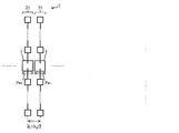
- the antenna elements are arranged in a grid pattern on a plane.
- the waveguide / transmission line converter 4 is arranged on a straight line in the horizontal direction of the drawing.
- the waveguide / transmission line converters 4 are arranged in a staggered manner in the left-right direction of the drawing.
- the antenna elements arranged in a lattice shape are divided into two rows of antenna elements 51. Each of the two rows of antenna elements 51 is connected to the waveguide / transmission line converter 4 arranged in the center of each of the two rows, and each of the two transmission lines 42 extends in the opposite direction (FIG. 8 as a third embodiment). The power is supplied as described above.
- the dielectric substrate 43 is a plane on which antenna elements are arranged in a lattice pattern.
- the cross section of the wide wall surface of the waveguide 41 is arranged in a direction perpendicular to the direction of each two rows.
- the cross section of the narrow wall surface of the waveguide 41 is arranged in a direction parallel to the direction of each two rows.
- the size p W3 in the direction along the cross section of the wide wall surface of the waveguide 41 among the sizes of the patterns arranged on the surface of the dielectric substrate 43 (see FIG. 8). Is the removal width 2nW3 or nW3 (see FIG. 8) of the metal member 45 and the ground metal layer 46 excluding the cross section of one of the two surfaces of the waveguide 41 or the narrow wall surface of one surface. )) Can be reduced.
- the size p W3 in FIG. 8 is about 2/3 in the millimeter wave application in which the dimension of the metal member 45 is not negligible compared to the size p W ′ in FIG.
- the distance d 3 of each row of antenna elements adjacent to each other may be narrower than a half length equal to lambda 0/2 of the wavelength lambda 0 of the electromagnetic wave has emitted.
- the waveguide / transmission line converter and the antenna device according to the present disclosure can form a high directivity with a high gain in any one direction in a wide frequency range with a combined result, hardly generate a grating lobe, and an antenna element on a plane
- the antenna device arranged in a lattice shape can be applied for the purpose of downsizing and cost reduction.
Landscapes
- Variable-Direction Aerials And Aerial Arrays (AREA)
Abstract
L'objet de la présente invention est : de réduire la taille, parmi les tailles d'un motif disposé sur une surface avers d'un substrat diélectrique, dans une direction le long d'une section transversale de surface de paroi large d'un tube de guide d'ondes, dans un convertisseur de tube de guide d'ondes/ligne de transmission; de réduire la séparation entre des rangées adjacentes d'éléments d'antenne, dans un dispositif d'antenne; et, concernant la directivité d'une antenne réseau formée au moyen des éléments d'antenne qui forment chaque rangée, d'ajuster en particulier des informations de phase de chaque élément d'antenne afin de réduire la probabilité que des lobes secondaires d'antenne réseau ne se produisent lorsqu'un faisceau est balayé sur un grand angle. Dans cette invention, une émission par inadvertance d'ondes électromagnétiques est évitée grâce à un agencement selon lequel un tube de guide d'ondes 11 s'étend à l'intérieur d'un substrat diélectrique 13, et selon lequel des éléments métalliques 15 permettant de maintenir une couche métallique de court-circuitage 14 au même potentiel que le tube de guide d'ondes 11 restent le long des deux sections transversales de surface de paroi large du tube de guide d'ondes 11, et sont retirés le long des deux sections transversales de surface de paroi étroite du tube de guide d'ondes 11.
Priority Applications (3)
| Application Number | Priority Date | Filing Date | Title |
|---|---|---|---|
| EP16768714.4A EP3276741B1 (fr) | 2015-03-23 | 2016-03-18 | Convertisseur de tube de guide d'ondes/ligne de transmission et dispositif d'antenne |
| US15/560,396 US10483611B2 (en) | 2015-03-23 | 2016-03-18 | Waveguide/transmission line converter configured to feed a plurality of antenna elements in an antenna device |
| CN201680016997.7A CN107408749B (zh) | 2015-03-23 | 2016-03-18 | 波导管/传输线路转换器和天线装置 |
Applications Claiming Priority (4)
| Application Number | Priority Date | Filing Date | Title |
|---|---|---|---|
| JP2015-058860 | 2015-03-23 | ||
| JP2015058860 | 2015-03-23 | ||
| JP2016016965A JP6721352B2 (ja) | 2015-03-23 | 2016-02-01 | 導波管/伝送線路変換器及びアンテナ装置 |
| JP2016-016965 | 2016-02-01 |
Publications (1)
| Publication Number | Publication Date |
|---|---|
| WO2016152811A1 true WO2016152811A1 (fr) | 2016-09-29 |
Family
ID=56978171
Family Applications (1)
| Application Number | Title | Priority Date | Filing Date |
|---|---|---|---|
| PCT/JP2016/058847 Ceased WO2016152811A1 (fr) | 2015-03-23 | 2016-03-18 | Convertisseur de tube de guide d'ondes/ligne de transmission et dispositif d'antenne |
Country Status (1)
| Country | Link |
|---|---|
| WO (1) | WO2016152811A1 (fr) |
Cited By (1)
| Publication number | Priority date | Publication date | Assignee | Title |
|---|---|---|---|---|
| CN109541744A (zh) * | 2017-09-22 | 2019-03-29 | 北京万集科技股份有限公司 | 一种基于反射层的硅基光学天线及制备方法 |
Citations (4)
| Publication number | Priority date | Publication date | Assignee | Title |
|---|---|---|---|---|
| GB2164497A (en) * | 1984-09-14 | 1986-03-19 | Singer Co | Interleaved microstrip antenna |
| JP2000244212A (ja) * | 1998-12-24 | 2000-09-08 | Toyota Central Res & Dev Lab Inc | 導波管・伝送線路変換器 |
| JP2010273029A (ja) * | 2009-05-20 | 2010-12-02 | Nec Corp | 半導体装置 |
| JP2014195327A (ja) * | 2014-06-11 | 2014-10-09 | Nippon Pillar Packing Co Ltd | 平面アンテナ |
-
2016
- 2016-03-18 WO PCT/JP2016/058847 patent/WO2016152811A1/fr not_active Ceased
Patent Citations (4)
| Publication number | Priority date | Publication date | Assignee | Title |
|---|---|---|---|---|
| GB2164497A (en) * | 1984-09-14 | 1986-03-19 | Singer Co | Interleaved microstrip antenna |
| JP2000244212A (ja) * | 1998-12-24 | 2000-09-08 | Toyota Central Res & Dev Lab Inc | 導波管・伝送線路変換器 |
| JP2010273029A (ja) * | 2009-05-20 | 2010-12-02 | Nec Corp | 半導体装置 |
| JP2014195327A (ja) * | 2014-06-11 | 2014-10-09 | Nippon Pillar Packing Co Ltd | 平面アンテナ |
Cited By (3)
| Publication number | Priority date | Publication date | Assignee | Title |
|---|---|---|---|---|
| CN109541744A (zh) * | 2017-09-22 | 2019-03-29 | 北京万集科技股份有限公司 | 一种基于反射层的硅基光学天线及制备方法 |
| CN109541744B (zh) * | 2017-09-22 | 2020-08-25 | 北京万集科技股份有限公司 | 一种基于反射层的硅基光学天线及制备方法 |
| US11194099B2 (en) | 2017-09-22 | 2021-12-07 | Vanjee Technology Co., Ltd. | Silicon-based optical antenna with reflective layer and preparation method therefor |
Similar Documents
| Publication | Publication Date | Title |
|---|---|---|
| JP6386182B2 (ja) | 導波管スロットアレイアンテナ | |
| JP5253468B2 (ja) | アンテナ装置及びレーダ装置 | |
| JP2006203899A (ja) | 一方向の放射パターンを有する小型超広帯域アンテナ | |
| CN104485500A (zh) | 波导微带线转换器 | |
| JP5788548B2 (ja) | マイクロストリップアンテナ | |
| WO2017216871A1 (fr) | Dispositif d'antenne réseau | |
| WO2007122782A1 (fr) | Antenne à fente | |
| JP5495955B2 (ja) | 導波管スロットアレーアンテナ | |
| WO2015118586A1 (fr) | Dispositif antenne | |
| JP6876942B2 (ja) | 回路基板 | |
| JP6611238B2 (ja) | 導波管/伝送線路変換器、アレーアンテナ及び平面アンテナ | |
| JP2008244520A (ja) | 平面アレーアンテナ | |
| JP2012070237A (ja) | マイクロストリップアレーアンテナ | |
| JP6613156B2 (ja) | 導波管/伝送線路変換器及びアンテナ装置 | |
| JP6721352B2 (ja) | 導波管/伝送線路変換器及びアンテナ装置 | |
| WO2016152811A1 (fr) | Convertisseur de tube de guide d'ondes/ligne de transmission et dispositif d'antenne | |
| JP6556406B2 (ja) | アンテナ装置 | |
| JP6613157B2 (ja) | 導波管/伝送線路変換器、アンテナ装置、及び、導波管/伝送線路変換器を製造する方法 | |
| JP5605285B2 (ja) | ダイポールアレーアンテナ | |
| JP2016178571A (ja) | 導波管/伝送線路変換器 | |
| JP5377070B2 (ja) | 導波管/マイクロストリップ線路変換器 | |
| US20180366826A1 (en) | Phase shift circuit and power supply circuit | |
| JP5317842B2 (ja) | アンテナ装置及びアレーアンテナ装置 | |
| JP3405233B2 (ja) | 導波管分岐回路及びアンテナ装置 | |
| JP5300571B2 (ja) | アンテナ装置 |
Legal Events
| Date | Code | Title | Description |
|---|---|---|---|
| 121 | Ep: the epo has been informed by wipo that ep was designated in this application |
Ref document number: 16768714 Country of ref document: EP Kind code of ref document: A1 |
|
| WWE | Wipo information: entry into national phase |
Ref document number: 15560396 Country of ref document: US |
|
| NENP | Non-entry into the national phase |
Ref country code: DE |
|
| REEP | Request for entry into the european phase |
Ref document number: 2016768714 Country of ref document: EP |