EP3281217B1 - Mehrfachband-photokathode - Google Patents
Mehrfachband-photokathode Download PDFInfo
- Publication number
- EP3281217B1 EP3281217B1 EP16722055.7A EP16722055A EP3281217B1 EP 3281217 B1 EP3281217 B1 EP 3281217B1 EP 16722055 A EP16722055 A EP 16722055A EP 3281217 B1 EP3281217 B1 EP 3281217B1
- Authority
- EP
- European Patent Office
- Prior art keywords
- layer
- elementary
- photocathode
- patterns
- emission
- Prior art date
- Legal status (The legal status is an assumption and is not a legal conclusion. Google has not performed a legal analysis and makes no representation as to the accuracy of the status listed.)
- Active
Links
Images




Classifications
-
- H—ELECTRICITY
- H01—ELECTRIC ELEMENTS
- H01J—ELECTRIC DISCHARGE TUBES OR DISCHARGE LAMPS
- H01J1/00—Details of electrodes, of magnetic control means, of screens, or of the mounting or spacing thereof, common to two or more basic types of discharge tubes or lamps
- H01J1/02—Main electrodes
- H01J1/34—Photo-emissive cathodes
-
- H—ELECTRICITY
- H01—ELECTRIC ELEMENTS
- H01J—ELECTRIC DISCHARGE TUBES OR DISCHARGE LAMPS
- H01J40/00—Photoelectric discharge tubes not involving the ionisation of a gas
- H01J40/02—Details
- H01J40/04—Electrodes
- H01J40/06—Photo-emissive cathodes
-
- H—ELECTRICITY
- H01—ELECTRIC ELEMENTS
- H01J—ELECTRIC DISCHARGE TUBES OR DISCHARGE LAMPS
- H01J40/00—Photoelectric discharge tubes not involving the ionisation of a gas
- H01J40/16—Photoelectric discharge tubes not involving the ionisation of a gas having photo- emissive cathode, e.g. alkaline photoelectric cell
-
- H—ELECTRICITY
- H01—ELECTRIC ELEMENTS
- H01J—ELECTRIC DISCHARGE TUBES OR DISCHARGE LAMPS
- H01J2201/00—Electrodes common to discharge tubes
- H01J2201/34—Photoemissive electrodes
- H01J2201/342—Cathodes
- H01J2201/3421—Composition of the emitting surface
- H01J2201/3423—Semiconductors, e.g. GaAs, NEA emitters
Definitions
- the present invention relates to the field of photocathodes, in particular for electromagnetic radiation detectors such as image intensifiers or sensors of EBCMOS ( Electron Bombarded CMOS ) or EBCDD ( Electron Bombarded CDD ) type. It is applicable in the field of night vision or infrared cameras.
- electromagnetic radiation detectors such as image intensifiers or sensors of EBCMOS ( Electron Bombarded CMOS ) or EBCDD ( Electron Bombarded CDD ) type. It is applicable in the field of night vision or infrared cameras.
- Electromagnetic radiation detectors such as, for example, image intensifier tubes and photomultiplier tubes, detect electromagnetic radiation by converting it into a light or electrical output signal.
- They usually comprise a photocathode for receiving the electromagnetic radiation and in response transmitting a photoelectron flux, an electron multiplier device for receiving said photoelectron flux and in response transmitting a flow of so-called secondary electrons, then an output device for receiving said secondary electron flow and in response transmitting the output signal.
- the output device may be a phosphor screen, providing a direct conversion into an image as in an image intensifier or a CCD or CMOS matrix to provide an electrical signal representative of the distribution of the incident photon flux.
- a photocathode usually comprises a layer, said window layer, transparent in the spectral band of interest, said window layer having a front face, said receiving face, for receiving the incident photons and a rear face which is opposite.
- An antireflection layer is deposited on the front face.
- An active layer is deposited on the rear face of the window layer. So the incident photons pass through the window layer from the receiving face, then enter the active layer where they generate electron-hole pairs.
- the electrons generated move to the emission face of the active layer and are emitted in vacuum.
- the photoelectrons are then directed and accelerated to an electron multiplier device such as a microchannel slab.
- the photocathodes are generally made of III-V semiconductor material such as GaAs. However, if the GaAs photocathodes have a good quantum yield in the visible spectrum (of the order of 40%) they are unusable in the near infrared, for wavelengths greater than 870nm (corresponding to the forbidden bandgap GaAs).
- the Fig. 1 represents a photocathode, 100, having a multilayer structure, known from the state of the art.
- This comprises a glass entrance window, 110, on which are deposited an anti-reflection layer, 121, and an electronic mirror, 122.
- the active layer, 130 located above the mirror consists of a superposition of N elementary layers, 130 1 , ..., 130 N Ga 1-x In x As, the concentration x indium being increasing in the direction of the incident flux.
- the forbidden bands of the successive elementary layers have forbidden band widths, E g1 ,..., E gN which are smaller and smaller in the direction of the incident flux, ie E g 1 > E g 2 >...> E gN .
- the first elementary layer 130 1 absorbs photons of energy greater than E g 1
- the second layer 130 2 absorbs photons not already absorbed and energy greater than E g 2 and so on.
- the electrons of the electron-hole pairs generated in an elemental layer diffuse up to the photoelectric emission face, 150, from where they are emitted in a vacuum and accelerated under the effect of the electric field.
- the electrons diffusing in the opposite direction of the incident flux are reflected by the band curvature induced by the electronic mirror.
- the electronic mirror consists of a semiconductor layer having a larger bandgap than that of the active layer.
- the mirror layer is made of GaAlAs when the active layer is GaInAs.
- Such a photocathode has sensitivity in both the visible spectrum (from 0.4 to 0.8 ⁇ m) and the near infrared spectrum ( ⁇ > 0.9 ⁇ m) or short wavelength IR (SWIR).
- SWIR short wavelength IR
- Such a photocathode generally has insufficient sensitivity in the visible spectrum. Indeed, the electrons generated in the first elementary layers of the active layer have a significant probability to recombine with holes or to be trapped by defects before reaching the photoelectric emission face.
- such a photocathode can not select the part of the spectrum that is to be imaged.
- a first object of the present invention is therefore to provide a photocathode having a high sensitivity (that is to say a quantum efficiency of the order of 25% or more), throughout the spectral range from visible to near infrared.
- a second aim of the present invention is to propose a detector capable of selecting a determined spectral band or even of dynamically switching from a first spectral band, such as that of the visible spectrum, to a second spectral band, such as that of the near infrared, and reciprocally.
- the present invention is defined by a photocathode comprising an input window for receiving an incident photon flux and an active layer on the input window opposite to the input face of the window, the active layer comprising a plurality of elementary layers of semiconductor materials having decreasing bandwidths in the direction of the incident photon flux, the surface of the photocathode opposite the input face being structured so that each elemental layer of the active layer has its own photoelectric emission surface.
- each elementary layer is formed by an array of patterns, the patterns of two successive elementary layers being interlaced.
- the active layer may consist of a first GaAs or GaAsP elemental layer and a second elementary layer in a semiconductor material selected from Ga 1-x In x As, GaAs 1-x Sb x , GaAs 1-x Bi x with 1 >x> 0.
- the different photoelectric emission surfaces of the elementary layers are covered by an activation layer.
- the active layer consists of a first elementary layer and a second elementary layer, the second elementary layer being covered by a transmission layer intended to emit in vacuum the photoelectrons generated in the second elementary layer, the first elementary layer having a first photoelectric emission surface and the emission layer having a second photoelectric emission surface.
- the first elementary layer is then connected to a first electrode and the emission layer is connected to a second electrode distinct from the first electrode so as to be able to carry the first and second electrodes at different potentials.
- the first and second photoelectric emission surfaces are covered by an activation layer.
- the photoelectric emission surface of the first elementary layer is typically formed by a first array of patterns, and the photoelectric emission surface of the emission layer is formed by a second array of patterns, the first and second patterns. networks being interlaced.
- the first and second pattern networks are periodic or pseudo-periodic.
- the first elementary layer may be InP
- the second GaInAs elementary layer GaInAsP, AlInAsP and the InP emission layer.
- the first elementary layer is made of GaAs, the second GaInAs elementary layer and the GaInP emission layer.
- the activation layer is for example Ag-Cs 2 O.
- the active layer is deposited on an electronic mirror constituted by a layer of a semiconductor material whose bandgap is greater than the bandgap widths of the elementary layers.
- the principle underlying the present invention is to use a photocathode of multilayer structure whose surface opposite to the entrance window is structured so that each elementary layer of the active layer has its own photoelectric emission surface .
- the photoelectric emission surface of each elementary layer is advantageously in the form of an array of patterns, the patterns of the various elementary layers being interlaced. More precisely, each elementary layer other than the first (in the direction of the incident flux) has a network of windows revealing the photoelectric emission face of the lower elementary layer.
- the Fig. 2 schematically shows the structure of a multilayer photocathode according to a first embodiment of the invention.
- This photocathode comprises a glass entrance window, 210, intended to receive the incident photon flux on which are advantageously deposited an antireflection layer, 221, and an electronic mirror, 222, the electronic mirror having the function of reflecting the photoelectrons generated.
- the active layer 230 is composed of a plurality of N elementary semiconductor layers of forbidden band widths decreasing in the direction of the flow of incident photons, that is to say the rear face to the front face of the active layer.
- the electronic mirror advantageously consists of a layer of semiconductor material having a band gap wider than those of the elementary layers of the active layer.
- the active layer consisted of a first elementary layer 230 1 having a first band gap E g 1 and a second elementary layer 230 2 having a second band gap E g 2 ⁇ E g 1 .
- the elementary layers are made of III-V semiconductor materials, for example ternary alloys of III-V materials such as Ga 1-x In x As, GaAs 1-x Sb x , GaAs 1-x Bi x where the concentration x increases in the direction of the flow of the incident photons.
- An electrode 270 makes it possible to polarize the photocathode negatively with respect to the anode of the detector in which it is intended to be mounted, for example an EBCMOS or EBCDD detector.
- the concentration x is chosen so to cover the desired spectral band.
- the electronic mirror can be made of GaAs.
- These different semiconductor layers are produced by epitaxy, for example by MOCVD ( Metal Organic Chemical Vapor Deposition ) or MBE ( Molecular Beam Epitaxy ), in a manner known per se.
- MOCVD Metal Organic Chemical Vapor Deposition
- MBE Molecular Beam Epitaxy
- the active layer is structured for example by means of differential etching. This structuring reveals a first emission surface photoelectric constituted by the zones 240 1 of the first elementary layer where the second elementary layer has been removed and a second photoelectric emission surface constituted by the zones 240 2 of the second elementary layer where it has been spared.
- the first photoelectric emission surface may be in the form of a first array of patterns on the surface of the first elemental layer.
- the second photoelectric emission surface may be in the form of a second array of patterns on the surface of the second elemental layer.
- the patterns of the first and second photoelectric emission surfaces are interleaved. In other words, except for the edges of the photocathode, a pattern of the second elementary layer is then located between two patterns of the first elementary layer.
- the photocathode has an active layer composed of N elementary semiconductor layers, each elementary layer having its own photoelectric emission surface.
- Each of the photoelectric emission surfaces may be in the form of an array of patterns, the patterns of the photoelectric emission surfaces of any two elementary layers of the active layer being then interwoven in the preceding sense.
- These patterns can be square, rectangular, hexagonal, annular, sectoral or even more complex.
- the patterns of the different photoelectric emission surfaces advantageously make it possible to tessellate the plane of the active layer.
- the sizes of the patterns and / or the pitches of the networks relating to the different elementary layers may be chosen different, on the basis of weighting criteria and spectral resolution as explained below.
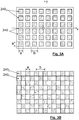
- the Fig. 3A represents a first example of structuring of the active layer.
- the photoelectric emission surface of the second elementary layer is in the form of an array of patterns of pitch b in the directions Ox and Oy of the plane, the patterns 240 2 being here of square shape and of size a ⁇ a .
- the photoelectric emission surface of the first elementary layer is formed by the residual zones 240 1 .
- the Fig. 3B represents a top view of a second example of structuring of the active layer.
- There is a first pattern grating, with pitch b 2 a in the directions Ox and Oy of the plane.
- the patterns 240 2 are also square in shape and of size a ⁇ a .
- the second network formed is the repetition of the patterns 240 2 and has the same characteristics as the first network, the first and second networks being interlaced.
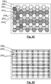
- the Fig. 3C represents a top view of a second example of structuring of the active layer.
- the respective patterns of the photoelectric emission surfaces associated with the various elementary layers have been noted 240 1 to 240 7 .
- the patterns here have a hexagonal shape and are interlaced so as to form a tiling of the plane of the active layer.
- the respective patterns of the different photoelectric emission surfaces have been designated 240 1 to 240 3 . Note that the patterns here are rectangular and of different sizes.
- the photoelectric emission surfaces of the various elementary layers are advantageously coated with a thin activation layer, for example a Cs 2 O layer or even a layer of Ag-Cs 2 O.
- This activation layer allows to lower the vacuum level below the level of the conduction band of the elementary layers it covers and thus facilitate the emission of photoelectrons in vacuum (photocathode negative electron affinity).
- the respective sizes and periodicities of the patterns of the various elementary semiconductor layers are chosen so as to weight the sensitivity of the photocathode in the different spectral bands.
- the photoelectrons emitted by the zones 240 1 of the first GaAs elementary layer correspond to the visible part of the spectrum.
- the photoelectrons emitted by the zones 240 2 can be either photoelectrons generated in the first elementary layer 230 1 having then diffused up to the photoelectric emission surface of the second elementary layer, or photoelectrons generated in the second elementary layer having diffused towards this same surface.
- the photoelectrons emitted by the zones 240 2 of the second elementary layer correspond to the visible spectrum (absorption by GaAs) or the spectrum in the near infrared (absorption by Ga 1-x In x As).
- the photoemission zones 240 1 and 240 2 of the first and second elementary layers are arranged in interlaced patterns. In other words, a pattern of one area is surrounded by patterns from another area. These patterns are arranged according to a periodic or pseudo-periodic network in the plane of the photocathode. For example, in Fig. 3B the patterns of the photoemission zones 240 1 and 240 2 are arranged according to two periodic gratings of pitch b / 2 in the directions Ox and Oy.
- the pitch of the elements of the EBCMOS or EBCDD sensor differs slightly from that of the periodic networks, a Moiré effect may appear.
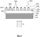
- the Fig. 4 schematically illustrates the structure of a multilayer photocathode according to a second embodiment of the invention.
- This photocathode comprises a glass entry window 410 for receiving the incident photon flux, on which an antireflection layer 421 and an electronic mirror 422 are advantageously deposited, as in the first embodiment.
- the active layer 430 is composed of a first elementary layer 430 1 in a first semiconductor material having a first band gap E g 1 and a second elementary layer 430 2 in a second semiconductor material having a band gap E g 2 less than the first band gap. These two elementary layers are photoelectron generation layers as in the first embodiment.
- An electrode 470 1 makes it possible to polarize the photocathode negatively with respect to the anode of the detector in which it is intended to be mounted, for example an EBCMOS or EBCDD detector.
- a photoelectron emission layer 440 is deposited on the active layer.
- This emission layer is made of a semiconductor material whose bandgap is greater than the bandgap of the second semiconductor material.
- the second elemental layer is p + doped at a doping level of the order 17 cm -3 .
- the emission layer is p-doped at a substantially lower doping level, of the order of 10 15 cm -3 .
- the emission layer is positively polarized with respect to the second elemental layer by means of the electrodes 470 2 so that the emission layer is depleted.
- the photoelectrons generated in the second elementary layer are found under the action of the electric field in the emission layer with a high energy level relative to the bottom of the conduction band of this layer. They then more easily cross the interface barrier with the thin activation layer (not shown) deposited on the emission layer.
- This photocathode structure is known as an electron transfer photocathode or TEP ( Tansfer Electron Photocathode ).
- TEP Tansfer Electron Photocathode
- a detailed description of an electron transfer photocathode can be found in the patent US-B-3958143 included here by reference.
- the first elementary layer of the active layer may for example be an InP layer and the second elementary layer may be for example a GaInAs layer.
- the emission layer may be an InP layer.
- the first elementary layer of the active layer may be a GaAs layer
- the second elementary layer may be a GaInAs layer
- the emission layer may be a layer of GalnP.
- the electronic mirror can be a layer of GaAIAs.
- the thin activation layer is, for example, a Cs 2 O or Ag-Cs 2 O layer deposited by vacuum evaporation. As indicated above, this layer makes it possible to lower the level of the vacuum and thus facilitates the photoelectric emission.
- the surface of the photocathode opposite the input window is structured so that the first elementary layer of the active layer has its own photoelectric emission surface.
- the emission layer and the second elementary layer are etched to the first elementary layer.
- a first photoelectric emission surface associated with the first elementary layer 430 1 and a second photoelectric emission surface associated with the emission layer 440 are obtained.
- the first photoelectric emission surface consists of zones 440 1 of the first elementary layer 430 1 and the second photoelectric emission surface consists of zones 440 2 of the emission layer, 440.
- the thin activation layer is deposited after the etching step so that it covers not only the zones 440 2 of the emission layer 440 but also the zones 440 1 of the first elementary layer 430 1 .
- the first elementary layer is connected to a first electrode 470 1 and the zones 440 2 of the emission layer 440 are connected to elementary electrodes 470 2 , forming a metal gate.
- the first elementary layer can be brought to a potential V 1 and the emission layer can be brought to a potential V 2 .
- the anode voltage V a of the detector is chosen such that V a > V 1 , V 2 .
- the zones 440 2 of the emission layer essentially emit photoelectrons generated in the second elementary layer.
- the zones 440 1 of the first elementary layer emit photoelectrons generated in the first elementary layer.
- zones 440 2 of the emission layer do not emit photoelectrons insofar as the latter do not have sufficient energy to pass over the interface barrier. Zones 440 1 continue to emit the photoelectrons generated in the first elementary layer. This gives an image in the visible spectrum only, I V.
- V 1 , V 2 can be obtained a visible image or an image in the spectrum SWIR, or a combination of these two images.
- the patterns 440 1 and 440 2 can be arranged according to periodic networks or, in case of Moiré effect, according to pseudo-periodic networks.
- the Fig. 5 represents the structure of a multilayer photocathode according to a variant of the first embodiment of the invention.
- the elements 510 to 540 1 -540 2 correspond to the elements 210 to 240 1 -240 2 of the Fig. 2 .
- the first elementary layer 530 1 of the active layer is first etched after masking the first patterns.
- the second elemental layer 530 2 is then grown by epitaxy in the wells obtained by etching to obtain the second units. After epitaxy of the second layer, mechanical polishing is carried out until the first elementary layer is flush with. A plane emission surface is thus obtained in which the first and second patterns alternate.
- the Fig. 6 represents the structure of a multilayer photocathode according to a variant of the second embodiment of the invention.
- the elements 610 to 670 1 -670 2 correspond to the elements 410 to 470 1 -470 2 of the Fig. 4 .
- This variant differs from that of the Fig. 4 in the sense that the first elementary layer 630 1 is etched after masking the first patterns.
- the second elemental layer 630 2 is then grown by epitaxy in the wells obtained by etching to obtain the second units.
- the emission layer of the photoelectrons 640 is grown before the mask is removed.
- the activation layer is then deposited over the entire surface before the electrodes 670 1 -670 2 are deposited.
Landscapes
- Common Detailed Techniques For Electron Tubes Or Discharge Tubes (AREA)
- Image-Pickup Tubes, Image-Amplification Tubes, And Storage Tubes (AREA)
Claims (14)
- Fotokathode, umfassend ein Eingangsfenster (210, 410, 510, 610), das dazu ausgelegt ist, einen Strom von einfallenden Photonen zu empfangen, sowie eine aktive Schicht auf dem Eingangsfenster entgegengesetzt zur Eingangsfläche des Fensters, wobei die aktive Schicht eine Mehrzahl von Elementarschichten (2301, .., 230N; 4301, ..,430N; 5301, .., 530N; 6301,..,630N) aus Halbleitermaterialien umfasst, die Breiten des verbotenen Bands haben, welche in der Richtung des Stroms von einfallenden Photonen abnehmen, wobei die Fotokathode dadurch gekennzeichnet ist, dass die Oberfläche der Fotokathode entgegengesetzt zur Eingangsfläche derart strukturiert ist, dass jede Elementarschicht der aktiven Schicht ihre eigene fotoelektrische Emissionsoberfläche (2401,..,240N; 4401,..,440N; 5401,..,540N; 6401,..,640N) besitzt.
- Fotokathode nach Anspruch 1, dadurch gekennzeichnet, dass die fotoelektrische Emissionsoberfläche jeder Elementarschicht durch ein Netz von Motiven gebildet ist, wobei die Motive von zwei aufeinanderfolgenden Elementarschichten verschachtelt sind.
- Fotokathode nach einem der vorhergehenden Ansprüche, dadurch gekennzeichnet, dass die aktive Schicht gebildet ist aus einer ersten Elementarschicht aus GaAs oder GaAsP und einer zweiten Elementarschicht aus einem Halbleitermaterial ausgewählt aus Ga1-xInxAs, GaAs1-xSbx, GaAs1-xBix mit 1>x>0.
- Fotokathode nach einem der vorhergehenden Ansprüche, dadurch gekennzeichnet, dass die verschiedenen fotoelektrischen Emissionsoberflächen der Elementarschichten mit einer Aktivierungsschicht bedeckt sind.
- Fotokathode nach Anspruch 1, dadurch gekennzeichnet, dass die aktive Schicht (430, 630) gebildet ist aus einer ersten Elementarschicht (4301, 6301) und einer zweiten Elementarschicht (4302, 6302), wobei die zweite Elementarschicht bedeckt ist durch eine Emissionsschicht (440, 640), die dazu ausgelegt ist, im Vakuum Fotoelektronen zu emittieren, die in der zweiten Elementarschicht generiert sind, wobei die erste Elementarschicht (4301, 6301) eine erste fotoelektrische Emissionsoberfläche (4401, 6401) besitzt, und wobei die Emissionsschicht eine zweite fotoelektrische Emissionsoberfläche (4402, 6402) besitzt.
- Fotokathode nach Anspruch 5, dadurch gekennzeichnet, dass die erste Elementarschicht (4301, 6301) mit einer ersten Elektrode (4701, 6701) verbunden ist, und dass die Emissionsschicht mit einer zweiten Elektrode (4702, 6702) verbunden ist, die von der ersten Elektrode verschieden ist, derart, dass die erste und die zweite Elektrode auf unterschiedliche Potentiale gebracht werden können.
- Fotokathode nach Anspruch 5 oder 6, dadurch gekennzeichnet, dass die erste und die zweite fotoelektrische Emissionsoberfläche durch eine Aktivierungsschicht bedeckt sind.
- Fotokathode nach einem der Ansprüche 6 bis 7, dadurch gekennzeichnet, dass die fotoelektrische Emissionsoberfläche der ersten Elementarschicht durch ein erste Netz von Motiven gebildet ist, und dass die fotoelektrische Emissionsoberfläche der Emissionsschicht durch ein zweites Netz von Motiven gebildet ist, wobei die Motive des ersten und des zweiten Netzes verschachtelt sind.
- Fotokathode nach Anspruch 8, dadurch gekennzeichnet, dass das erste und das zweite Netz von Motiven periodisch sind.
- Fotokathode nach Anspruch 8, dadurch gekennzeichnet, dass das erste und das zweite Netz pseudoperiodisch sind.
- Fotokathode nach einem der Ansprüche 5 bis 10, dadurch gekennzeichnet, dass die erste Elementarschicht aus InP ist, dass die zweite Elementarschicht aus GaInAs, GaInAsP, AlInAsP ist, und dass die Emissionsschicht aus InP ist.
- Fotokathode nach einem der Ansprüche 5 bis 10, dadurch gekennzeichnet, dass die erste Elementarschicht aus GaAs ist, dass die zweite Elementarschicht aus GaInAs ist, und dass die Emissionsschicht aus GaInP ist.
- Fotokathode nach einem der Ansprüche 4, 7 und 8 bis 12 in Abhängigkeit von Anspruch 7, dadurch gekennzeichnet, dass die Aktivierungsschicht aus Ag-Cs2O ist.
- Fotokathode nach einem der vorhergehenden Ansprüche, dadurch gekennzeichnet, dass die aktive Schicht aufgebracht ist auf einem elektronischen Spiegel der Fotokathode, gebildet durch eine Schicht aus einem Halbleitermaterial, bei dem die Breite des verbotenen Bands größer ist als die Breiten der verbotenen Bänder der Elementarschichten.
Applications Claiming Priority (2)
| Application Number | Priority Date | Filing Date | Title |
|---|---|---|---|
| FR1553027A FR3034908B1 (fr) | 2015-04-08 | 2015-04-08 | Photocathode multibande et detecteur associe |
| PCT/EP2016/057468 WO2016162351A1 (fr) | 2015-04-08 | 2016-04-06 | Photocathode multibande et détecteur associé |
Publications (2)
| Publication Number | Publication Date |
|---|---|
| EP3281217A1 EP3281217A1 (de) | 2018-02-14 |
| EP3281217B1 true EP3281217B1 (de) | 2018-12-12 |
Family
ID=54260837
Family Applications (1)
| Application Number | Title | Priority Date | Filing Date |
|---|---|---|---|
| EP16722055.7A Active EP3281217B1 (de) | 2015-04-08 | 2016-04-06 | Mehrfachband-photokathode |
Country Status (7)
| Country | Link |
|---|---|
| US (1) | US10186405B2 (de) |
| EP (1) | EP3281217B1 (de) |
| JP (1) | JP6893881B2 (de) |
| KR (1) | KR102567402B1 (de) |
| FR (1) | FR3034908B1 (de) |
| IL (1) | IL254810B (de) |
| WO (1) | WO2016162351A1 (de) |
Families Citing this family (4)
| Publication number | Priority date | Publication date | Assignee | Title |
|---|---|---|---|---|
| FR3051963B1 (fr) | 2016-05-31 | 2020-12-25 | Photonis France | Photocathode a nanofils et methode de fabrication d'une telle photocathode |
| US10763092B2 (en) * | 2017-11-29 | 2020-09-01 | L-3 Communications Corporation-Insight Technology Division | Dual-spectrum photocathode for image intensification |
| CN111613497B (zh) * | 2020-06-05 | 2023-05-12 | 陕西理工大学 | 一种分光谱响应增强的透射式光电阴极及其制备方法 |
| US12334321B1 (en) | 2024-08-07 | 2025-06-17 | L3Harris Technologies, Inc. | And manufacturing methods of SWIR I2TUBE via heterogeneous wafer integration |
Family Cites Families (15)
| Publication number | Priority date | Publication date | Assignee | Title |
|---|---|---|---|---|
| US3958143A (en) * | 1973-01-15 | 1976-05-18 | Varian Associates | Long-wavelength photoemission cathode |
| JPS5430774A (en) * | 1977-08-12 | 1979-03-07 | Hitachi Denshi Ltd | Manufacture of photo-electron emissibe surface |
| US5471051A (en) * | 1993-06-02 | 1995-11-28 | Hamamatsu Photonics K.K. | Photocathode capable of detecting position of incident light in one or two dimensions, phototube, and photodetecting apparatus containing same |
| JP2923462B2 (ja) * | 1994-12-21 | 1999-07-26 | 浜松ホトニクス株式会社 | 光電陰極および電子管 |
| US5932966A (en) * | 1995-07-10 | 1999-08-03 | Intevac, Inc. | Electron sources utilizing patterned negative electron affinity photocathodes |
| US6005257A (en) * | 1995-09-13 | 1999-12-21 | Litton Systems, Inc. | Transmission mode photocathode with multilayer active layer for night vision and method |
| US6069445A (en) * | 1997-01-30 | 2000-05-30 | Itt Industries, Inc. | Having an electrical contact on an emission surface thereof |
| JP3623068B2 (ja) * | 1997-02-28 | 2005-02-23 | 浜松ホトニクス株式会社 | 光電陰極 |
| JP2002184302A (ja) * | 2000-12-18 | 2002-06-28 | Hamamatsu Photonics Kk | 半導体光電陰極 |
| JP4002167B2 (ja) * | 2002-11-14 | 2007-10-31 | 浜松ホトニクス株式会社 | 光電陰極 |
| US6998635B2 (en) * | 2003-05-22 | 2006-02-14 | Itt Manufacturing Enterprises Inc. | Tuned bandwidth photocathode for transmission negative electron affinity devices |
| JP4647955B2 (ja) * | 2004-08-17 | 2011-03-09 | 浜松ホトニクス株式会社 | 光電陰極板及び電子管 |
| US7592747B1 (en) * | 2005-02-09 | 2009-09-22 | The United States Of America As Represented By The National Aeronautics And Space Administration | Piezoelectrically enhanced photocathode |
| JP5135114B2 (ja) * | 2008-08-06 | 2013-01-30 | 浜松ホトニクス株式会社 | 光電陰極およびその製造方法並びに光電子増倍管 |
| JP6200175B2 (ja) * | 2012-03-23 | 2017-09-20 | サンケン電気株式会社 | 半導体光電陰極及びその製造方法、電子管並びにイメージ増強管 |
-
2015
- 2015-04-08 FR FR1553027A patent/FR3034908B1/fr not_active Expired - Fee Related
-
2016
- 2016-04-06 KR KR1020177027947A patent/KR102567402B1/ko active Active
- 2016-04-06 EP EP16722055.7A patent/EP3281217B1/de active Active
- 2016-04-06 US US15/564,880 patent/US10186405B2/en active Active
- 2016-04-06 WO PCT/EP2016/057468 patent/WO2016162351A1/fr not_active Ceased
- 2016-04-06 JP JP2017553020A patent/JP6893881B2/ja active Active
-
2017
- 2017-10-01 IL IL254810A patent/IL254810B/en unknown
Non-Patent Citations (1)
| Title |
|---|
| None * |
Also Published As
| Publication number | Publication date |
|---|---|
| JP2018514063A (ja) | 2018-05-31 |
| IL254810B (en) | 2022-02-01 |
| KR102567402B1 (ko) | 2023-08-22 |
| KR20170133368A (ko) | 2017-12-05 |
| EP3281217A1 (de) | 2018-02-14 |
| FR3034908B1 (fr) | 2017-05-05 |
| FR3034908A1 (fr) | 2016-10-14 |
| US20180096829A1 (en) | 2018-04-05 |
| US10186405B2 (en) | 2019-01-22 |
| JP6893881B2 (ja) | 2021-06-23 |
| IL254810A0 (en) | 2017-12-31 |
| WO2016162351A1 (fr) | 2016-10-13 |
Similar Documents
| Publication | Publication Date | Title |
|---|---|---|
| EP2180512B1 (de) | Vorrichtung zur polarimetrischen Bildgebung, die im Hinblick auf den Polarisationskontrast optimiert ist | |
| EP3104421B1 (de) | Mit einem gitter abgedeckte spad-fotodiode | |
| WO2020007622A1 (fr) | Détecteur bi-spectral amélioré | |
| EP3084843B1 (de) | Quantendetektionselement mit geringem rauschen und verfahren zur herstellung solch eines lichtdetektionselements | |
| EP2180511B1 (de) | Vorrichtung zur multispektralen Bildgebung auf der Grundlage von Mehrfachquantentöpfen | |
| EP3281217B1 (de) | Mehrfachband-photokathode | |
| EP3012876A1 (de) | Herstellungsverfahren einer rauscharmen fotodiode | |
| EP3465725B1 (de) | Verfahren zur herstellung einer nanodrahtfotokathode | |
| EP1756872B1 (de) | Mesastruktur-photonerkennungschaltung | |
| EP1903612B1 (de) | Fotodiode mit Lawine | |
| EP3871273A1 (de) | Verfahren zur herstellung einer optoelektronischen vorrichtung mit mehrdimensionalen homogenen leuchtdioden | |
| EP3471151B1 (de) | Helmholtz-resonator-photodetektor | |
| EP0477086A1 (de) | Lichtfrequenzwandler | |
| EP3871272A1 (de) | Optoelektronische vorrichtung, zugehöriger bildschirm und verfahren zur herstellung einer solchen optoelektronischen vorrichtung | |
| Destefanis et al. | Bi-color and dual-band HgCdTe infrared focal plane arrays at DEFIR | |
| EP3664141B1 (de) | Matrix von peripheren absorptions-fotodetektoren mit fokussierungsstrukturen | |
| EP3662511B1 (de) | Verbesserter infrarotdetektor | |
| WO2017032955A1 (fr) | Matrice de photodiodes a cathodes isolees | |
| WO2014187840A1 (fr) | Matrice de photodiode à absorption réglable de charge |
Legal Events
| Date | Code | Title | Description |
|---|---|---|---|
| STAA | Information on the status of an ep patent application or granted ep patent |
Free format text: STATUS: THE INTERNATIONAL PUBLICATION HAS BEEN MADE |
|
| PUAI | Public reference made under article 153(3) epc to a published international application that has entered the european phase |
Free format text: ORIGINAL CODE: 0009012 |
|
| STAA | Information on the status of an ep patent application or granted ep patent |
Free format text: STATUS: REQUEST FOR EXAMINATION WAS MADE |
|
| 17P | Request for examination filed |
Effective date: 20171009 |
|
| AK | Designated contracting states |
Kind code of ref document: A1 Designated state(s): AL AT BE BG CH CY CZ DE DK EE ES FI FR GB GR HR HU IE IS IT LI LT LU LV MC MK MT NL NO PL PT RO RS SE SI SK SM TR |
|
| AX | Request for extension of the european patent |
Extension state: BA ME |
|
| RIN1 | Information on inventor provided before grant (corrected) |
Inventor name: CONDE, MOUSTAPHA Inventor name: FOLTZ, JUSTIN |
|
| DAV | Request for validation of the european patent (deleted) | ||
| DAX | Request for extension of the european patent (deleted) | ||
| GRAP | Despatch of communication of intention to grant a patent |
Free format text: ORIGINAL CODE: EPIDOSNIGR1 |
|
| STAA | Information on the status of an ep patent application or granted ep patent |
Free format text: STATUS: GRANT OF PATENT IS INTENDED |
|
| INTG | Intention to grant announced |
Effective date: 20180810 |
|
| GRAS | Grant fee paid |
Free format text: ORIGINAL CODE: EPIDOSNIGR3 |
|
| GRAA | (expected) grant |
Free format text: ORIGINAL CODE: 0009210 |
|
| STAA | Information on the status of an ep patent application or granted ep patent |
Free format text: STATUS: THE PATENT HAS BEEN GRANTED |
|
| AK | Designated contracting states |
Kind code of ref document: B1 Designated state(s): AL AT BE BG CH CY CZ DE DK EE ES FI FR GB GR HR HU IE IS IT LI LT LU LV MC MK MT NL NO PL PT RO RS SE SI SK SM TR |
|
| REG | Reference to a national code |
Ref country code: GB Ref legal event code: FG4D Free format text: NOT ENGLISH |
|
| REG | Reference to a national code |
Ref country code: CH Ref legal event code: EP |
|
| REG | Reference to a national code |
Ref country code: AT Ref legal event code: REF Ref document number: 1077093 Country of ref document: AT Kind code of ref document: T Effective date: 20181215 |
|
| REG | Reference to a national code |
Ref country code: DE Ref legal event code: R096 Ref document number: 602016008234 Country of ref document: DE |
|
| REG | Reference to a national code |
Ref country code: IE Ref legal event code: FG4D Free format text: LANGUAGE OF EP DOCUMENT: FRENCH |
|
| REG | Reference to a national code |
Ref country code: NL Ref legal event code: FP |
|
| REG | Reference to a national code |
Ref country code: LT Ref legal event code: MG4D |
|
| PG25 | Lapsed in a contracting state [announced via postgrant information from national office to epo] |
Ref country code: ES Free format text: LAPSE BECAUSE OF FAILURE TO SUBMIT A TRANSLATION OF THE DESCRIPTION OR TO PAY THE FEE WITHIN THE PRESCRIBED TIME-LIMIT Effective date: 20181212 Ref country code: BG Free format text: LAPSE BECAUSE OF FAILURE TO SUBMIT A TRANSLATION OF THE DESCRIPTION OR TO PAY THE FEE WITHIN THE PRESCRIBED TIME-LIMIT Effective date: 20190312 Ref country code: NO Free format text: LAPSE BECAUSE OF FAILURE TO SUBMIT A TRANSLATION OF THE DESCRIPTION OR TO PAY THE FEE WITHIN THE PRESCRIBED TIME-LIMIT Effective date: 20190312 Ref country code: FI Free format text: LAPSE BECAUSE OF FAILURE TO SUBMIT A TRANSLATION OF THE DESCRIPTION OR TO PAY THE FEE WITHIN THE PRESCRIBED TIME-LIMIT Effective date: 20181212 Ref country code: LT Free format text: LAPSE BECAUSE OF FAILURE TO SUBMIT A TRANSLATION OF THE DESCRIPTION OR TO PAY THE FEE WITHIN THE PRESCRIBED TIME-LIMIT Effective date: 20181212 Ref country code: LV Free format text: LAPSE BECAUSE OF FAILURE TO SUBMIT A TRANSLATION OF THE DESCRIPTION OR TO PAY THE FEE WITHIN THE PRESCRIBED TIME-LIMIT Effective date: 20181212 Ref country code: HR Free format text: LAPSE BECAUSE OF FAILURE TO SUBMIT A TRANSLATION OF THE DESCRIPTION OR TO PAY THE FEE WITHIN THE PRESCRIBED TIME-LIMIT Effective date: 20181212 |
|
| REG | Reference to a national code |
Ref country code: AT Ref legal event code: MK05 Ref document number: 1077093 Country of ref document: AT Kind code of ref document: T Effective date: 20181212 |
|
| PG25 | Lapsed in a contracting state [announced via postgrant information from national office to epo] |
Ref country code: SE Free format text: LAPSE BECAUSE OF FAILURE TO SUBMIT A TRANSLATION OF THE DESCRIPTION OR TO PAY THE FEE WITHIN THE PRESCRIBED TIME-LIMIT Effective date: 20181212 Ref country code: RS Free format text: LAPSE BECAUSE OF FAILURE TO SUBMIT A TRANSLATION OF THE DESCRIPTION OR TO PAY THE FEE WITHIN THE PRESCRIBED TIME-LIMIT Effective date: 20181212 Ref country code: AL Free format text: LAPSE BECAUSE OF FAILURE TO SUBMIT A TRANSLATION OF THE DESCRIPTION OR TO PAY THE FEE WITHIN THE PRESCRIBED TIME-LIMIT Effective date: 20181212 Ref country code: GR Free format text: LAPSE BECAUSE OF FAILURE TO SUBMIT A TRANSLATION OF THE DESCRIPTION OR TO PAY THE FEE WITHIN THE PRESCRIBED TIME-LIMIT Effective date: 20190313 |
|
| PG25 | Lapsed in a contracting state [announced via postgrant information from national office to epo] |
Ref country code: PT Free format text: LAPSE BECAUSE OF FAILURE TO SUBMIT A TRANSLATION OF THE DESCRIPTION OR TO PAY THE FEE WITHIN THE PRESCRIBED TIME-LIMIT Effective date: 20190412 Ref country code: PL Free format text: LAPSE BECAUSE OF FAILURE TO SUBMIT A TRANSLATION OF THE DESCRIPTION OR TO PAY THE FEE WITHIN THE PRESCRIBED TIME-LIMIT Effective date: 20181212 Ref country code: CZ Free format text: LAPSE BECAUSE OF FAILURE TO SUBMIT A TRANSLATION OF THE DESCRIPTION OR TO PAY THE FEE WITHIN THE PRESCRIBED TIME-LIMIT Effective date: 20181212 Ref country code: IT Free format text: LAPSE BECAUSE OF FAILURE TO SUBMIT A TRANSLATION OF THE DESCRIPTION OR TO PAY THE FEE WITHIN THE PRESCRIBED TIME-LIMIT Effective date: 20181212 |
|
| PG25 | Lapsed in a contracting state [announced via postgrant information from national office to epo] |
Ref country code: IS Free format text: LAPSE BECAUSE OF FAILURE TO SUBMIT A TRANSLATION OF THE DESCRIPTION OR TO PAY THE FEE WITHIN THE PRESCRIBED TIME-LIMIT Effective date: 20190412 Ref country code: EE Free format text: LAPSE BECAUSE OF FAILURE TO SUBMIT A TRANSLATION OF THE DESCRIPTION OR TO PAY THE FEE WITHIN THE PRESCRIBED TIME-LIMIT Effective date: 20181212 Ref country code: SM Free format text: LAPSE BECAUSE OF FAILURE TO SUBMIT A TRANSLATION OF THE DESCRIPTION OR TO PAY THE FEE WITHIN THE PRESCRIBED TIME-LIMIT Effective date: 20181212 Ref country code: RO Free format text: LAPSE BECAUSE OF FAILURE TO SUBMIT A TRANSLATION OF THE DESCRIPTION OR TO PAY THE FEE WITHIN THE PRESCRIBED TIME-LIMIT Effective date: 20181212 Ref country code: SK Free format text: LAPSE BECAUSE OF FAILURE TO SUBMIT A TRANSLATION OF THE DESCRIPTION OR TO PAY THE FEE WITHIN THE PRESCRIBED TIME-LIMIT Effective date: 20181212 |
|
| REG | Reference to a national code |
Ref country code: DE Ref legal event code: R097 Ref document number: 602016008234 Country of ref document: DE |
|
| PLBE | No opposition filed within time limit |
Free format text: ORIGINAL CODE: 0009261 |
|
| STAA | Information on the status of an ep patent application or granted ep patent |
Free format text: STATUS: NO OPPOSITION FILED WITHIN TIME LIMIT |
|
| PG25 | Lapsed in a contracting state [announced via postgrant information from national office to epo] |
Ref country code: DK Free format text: LAPSE BECAUSE OF FAILURE TO SUBMIT A TRANSLATION OF THE DESCRIPTION OR TO PAY THE FEE WITHIN THE PRESCRIBED TIME-LIMIT Effective date: 20181212 Ref country code: AT Free format text: LAPSE BECAUSE OF FAILURE TO SUBMIT A TRANSLATION OF THE DESCRIPTION OR TO PAY THE FEE WITHIN THE PRESCRIBED TIME-LIMIT Effective date: 20181212 |
|
| 26N | No opposition filed |
Effective date: 20190913 |
|
| REG | Reference to a national code |
Ref country code: CH Ref legal event code: PL |
|
| REG | Reference to a national code |
Ref country code: BE Ref legal event code: MM Effective date: 20190430 |
|
| PG25 | Lapsed in a contracting state [announced via postgrant information from national office to epo] |
Ref country code: LU Free format text: LAPSE BECAUSE OF NON-PAYMENT OF DUE FEES Effective date: 20190406 Ref country code: MC Free format text: LAPSE BECAUSE OF FAILURE TO SUBMIT A TRANSLATION OF THE DESCRIPTION OR TO PAY THE FEE WITHIN THE PRESCRIBED TIME-LIMIT Effective date: 20181212 |
|
| PG25 | Lapsed in a contracting state [announced via postgrant information from national office to epo] |
Ref country code: CH Free format text: LAPSE BECAUSE OF NON-PAYMENT OF DUE FEES Effective date: 20190430 Ref country code: LI Free format text: LAPSE BECAUSE OF NON-PAYMENT OF DUE FEES Effective date: 20190430 |
|
| PG25 | Lapsed in a contracting state [announced via postgrant information from national office to epo] |
Ref country code: BE Free format text: LAPSE BECAUSE OF NON-PAYMENT OF DUE FEES Effective date: 20190430 |
|
| PG25 | Lapsed in a contracting state [announced via postgrant information from national office to epo] |
Ref country code: TR Free format text: LAPSE BECAUSE OF FAILURE TO SUBMIT A TRANSLATION OF THE DESCRIPTION OR TO PAY THE FEE WITHIN THE PRESCRIBED TIME-LIMIT Effective date: 20181212 |
|
| PG25 | Lapsed in a contracting state [announced via postgrant information from national office to epo] |
Ref country code: IE Free format text: LAPSE BECAUSE OF NON-PAYMENT OF DUE FEES Effective date: 20190406 |
|
| PG25 | Lapsed in a contracting state [announced via postgrant information from national office to epo] |
Ref country code: CY Free format text: LAPSE BECAUSE OF FAILURE TO SUBMIT A TRANSLATION OF THE DESCRIPTION OR TO PAY THE FEE WITHIN THE PRESCRIBED TIME-LIMIT Effective date: 20181212 |
|
| PG25 | Lapsed in a contracting state [announced via postgrant information from national office to epo] |
Ref country code: HU Free format text: LAPSE BECAUSE OF FAILURE TO SUBMIT A TRANSLATION OF THE DESCRIPTION OR TO PAY THE FEE WITHIN THE PRESCRIBED TIME-LIMIT; INVALID AB INITIO Effective date: 20160406 Ref country code: MT Free format text: LAPSE BECAUSE OF FAILURE TO SUBMIT A TRANSLATION OF THE DESCRIPTION OR TO PAY THE FEE WITHIN THE PRESCRIBED TIME-LIMIT Effective date: 20181212 |
|
| PG25 | Lapsed in a contracting state [announced via postgrant information from national office to epo] |
Ref country code: SI Free format text: LAPSE BECAUSE OF FAILURE TO SUBMIT A TRANSLATION OF THE DESCRIPTION OR TO PAY THE FEE WITHIN THE PRESCRIBED TIME-LIMIT Effective date: 20181212 |
|
| PG25 | Lapsed in a contracting state [announced via postgrant information from national office to epo] |
Ref country code: MK Free format text: LAPSE BECAUSE OF FAILURE TO SUBMIT A TRANSLATION OF THE DESCRIPTION OR TO PAY THE FEE WITHIN THE PRESCRIBED TIME-LIMIT Effective date: 20181212 |
|
| P01 | Opt-out of the competence of the unified patent court (upc) registered |
Effective date: 20230526 |
|
| REG | Reference to a national code |
Ref country code: DE Ref legal event code: R082 Ref document number: 602016008234 Country of ref document: DE Representative=s name: LAURENT CHARRAS, FR Ref country code: DE Ref legal event code: R082 Ref document number: 602016008234 Country of ref document: DE Representative=s name: VUILLERMOZ, BRUNO, FR |
|
| PGFP | Annual fee paid to national office [announced via postgrant information from national office to epo] |
Ref country code: DE Payment date: 20250411 Year of fee payment: 10 |
|
| PGFP | Annual fee paid to national office [announced via postgrant information from national office to epo] |
Ref country code: GB Payment date: 20250417 Year of fee payment: 10 |
|
| PGFP | Annual fee paid to national office [announced via postgrant information from national office to epo] |
Ref country code: FR Payment date: 20250428 Year of fee payment: 10 |
|
| REG | Reference to a national code |
Ref country code: DE Ref legal event code: R082 Ref document number: 602016008234 Country of ref document: DE Representative=s name: VUILLERMOZ, BRUNO, FR |
|
| PGFP | Annual fee paid to national office [announced via postgrant information from national office to epo] |
Ref country code: NL Payment date: 20260326 Year of fee payment: 11 |